J. Semicond. > 2021, Volume 42 > Issue 8 > 082901

ARTICLES

Targeted transfer of self-assembled CdSe nanoplatelet film onto WS2 flakes to construct hybrid heterostructures

Zeguo Song1, Yunkun Wang1, Yunke Zhu1, Peng Bai1, An Hu1 and Yunan Gao1, 2, 3,

+ Author Affiliations

 Corresponding author: Yunan Gao, gyn@pku.edu.cn

DOI: 10.1088/1674-4926/42/8/082901

PDF

Turn off MathJax

Abstract: Colloidal CdSe nanoplatelets are thin semiconductor materials with atomic flatness surfaces and one-dimensional strong quantum confinement, and hence they own very narrow and anisotropic emission. Here, we present a polydimethylsiloxane (PDMS) assisted transferring method that can pick up single layer CdSe nanoplatelet films self-assembled on a liquid surface and then precisely transfer to a target. By layer-by-layer picking up and transferring, multiple layers of CdSe films can be built up to form CdSe stacks with each single layer having dominant in-plane transition dipole distribution, which both material and energic structures are analogous to traditional multiple quantum wells grown by molecular-beam epitaxy. Additionally, with the great flexibility of colloidal nanoplatelets and this transferring method, CdSe nanoplatelets films can be combined with other materials to form hybrid heterostructures. We transferred a single-layer CdSe film onto WS2 flakes, and precisely studied the fast energy transfer rate with controlled CdSe nanoplatelet orientation and by using a streak camera with a ps time resolution.

Key words: CdSe nanoplateletsself-assemblytransferenergy transferhybrid heterostructuresWS2

Colloidal semiconductor nanocrystals have been intensively studied for several decades, and various types in chemical compositions, shapes and sizes can be synthesized[1]. CdSe nanoplatelets, as one type of nanocrystal with an anisotropic shape, attracted increasing interest in recent years, because they have very sharp emission peaks and pure in-plane transition dipoles[2-4]. They are very promising for developing low-cost and highly efficient nanocrystal-based light emitting diodes and lasers[5-9].

For controlling these nanocrystals to build macro-scale functional materials, self-assembly of them has been considered as the most promising method[10-14]. Several groups have used liquid surface self-assembly to successfully have CdSe nanoplatelet oriented in either face-down or side-up configuration[2, 15-17]. For further property studies and applications, the self-assembled films need to transfer on solid substrates. Typically, it was achieved by submerging the targeted substrate into the supporting liquid and then draining the liquid away[2, 15, 17]. This strategy, although workable, has several drawbacks as that the targeted samples have to be stable against the supporting liquid and should have sufficient size to avoid misalignment. Bai et al. used ink-jet printing to directly assemble nanoplatelets to uniform films with a size of tens of micrometers on a number of substrates[18]. For this method, the surface properties of the targets have to be properly controlled to allow the nanoplatelet to assemble during the drying process. While controllable self-assembly of nanocrystals has achieved significant progress, transferring methods are not yet well developed.

In this work, we report a fascinate method that can pick up the self-assembled single-layer CdSe films suspended on acetonitrile and then precisely transfer onto targeted substrates. Combining transmission electron microscopy (TEM), atomic force microscopy (AFM) and back focal plane imaging (BFP), we determined that the films exhibit an around 90% in-plane transition dipole distribution. Using this method, it is very convenient to construct hybrid heterostructure combining colloidal quantum dots with other structures and/or materials, in which new properties can be exploited[19-24]. Herein, we transferred a single-layer CdSe film onto a WS2 flake. With the controlled nanoplatelet orientation and using ps time-resolved streak camera, the energy transfer rate between these two types of two-dimensional materials is precisely determined.

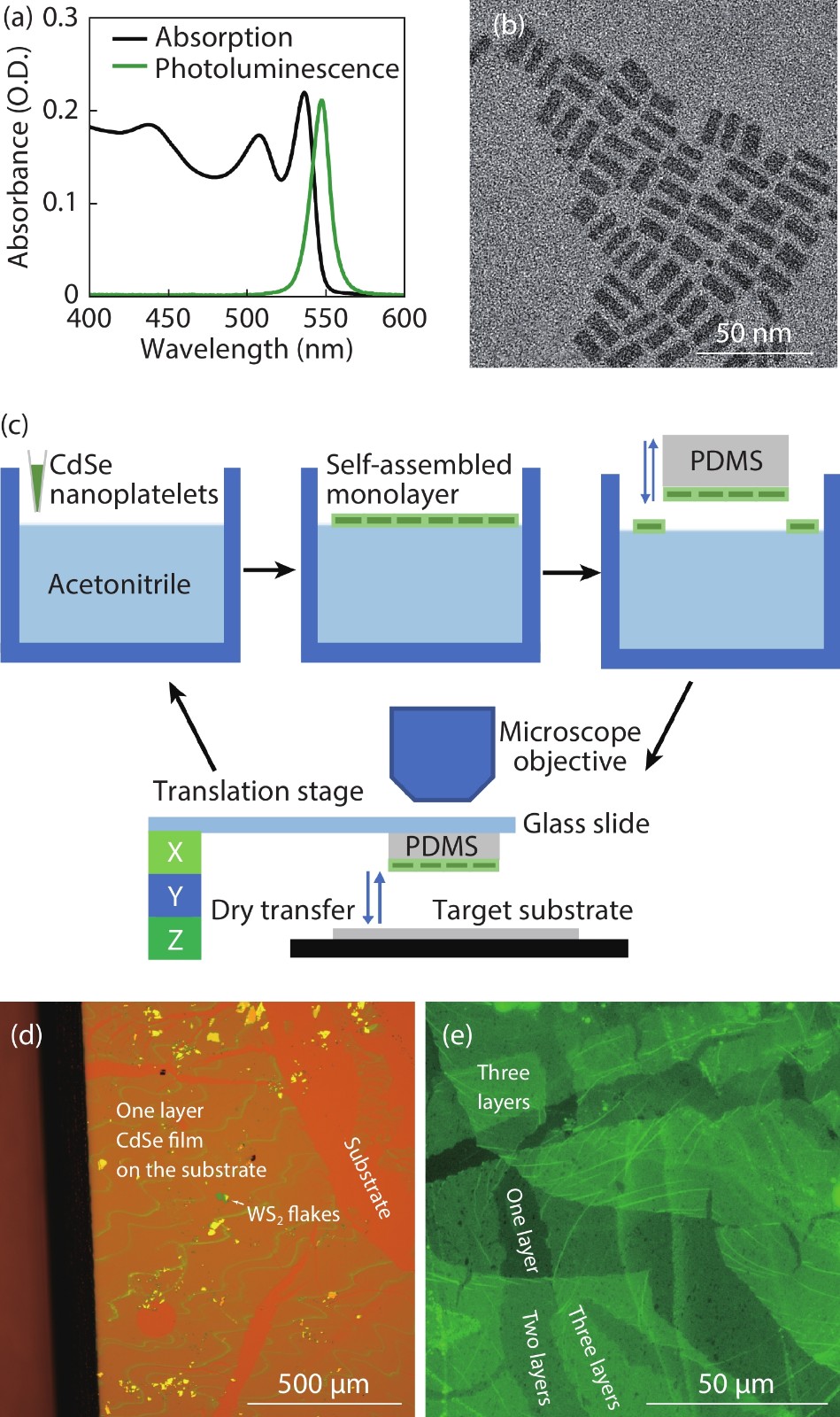
CdSe nanoplatelets were synthesized following Ref. [25], and the absorption and photoluminescence spectra are presented in Fig. 1(a). A TEM image of these nanoplatelets all laying face-down on a TEM grid is presented in Fig. 1(b), from which the length and width are determined to be 18 × 5 nm2. The thickness of the nanoplatelets is 1.5 nm, which has been well documented in literature for CdSe nanoplatelets with the emission peak at 550 nm[25]. Fig. 1(c) illustrates the PDMS-assisted transferring method. Self-assembly of the CdSe nanoplatelet single layer was carried out by adding a small amount of CdSe nanoplatelets dispersed in hexane on top of acetonitrile. After the hexane evaporated, a single layer of the nanoplatelet film was left on the acetonitrile surface. A PDMS stamp was bought close to the surface slowly using a motorized translation stage to pick up the film. For transferring, the PDMS stamp was mounted on a glass slide. Monitored in microscopy, the stamp was brought close to the target substrate slowly by a motorized translation stage. Fig. 1(d) shows a bright-field microscopy image of a layer of CdSe nanoplatelets transferred on a SiO2/Si substrate with WS2 flakes mechanically exfoliated in advance. Multilayer films could be built up by repeating the whole process described above with the substrate heated up to 85 °C by a hotplate, hold for 30 s and cooled down quickly by a water chiller. Fig. 1(e) shows a photoluminescence image of nanoplatelet films on a cover glass substrate with one, two and three layers of CdSe nanoplatelets in different areas. Shortly heating the CdSe nanoplatelet films at a moderate temperature of 85 °C did not decrease their photoluminescence brightness. We noticed that the nanoplatelet film could be directly transferred on a glass substrate at room temperature while the subsequent transfers required a raised temperature. The relative strengths of the interface interaction between substrate/nanoplatelets, nanoplatelets/nanoplatelets, and nanoplatelet/PDMS, determine whether the nanoplatelet film can be transferred onto the target. Increasing the temperature decreases the viscosity of PDMS and helps to release the CdSe nanoplatelet films.

Figure  1.  (Color online) (a) Absorption and photoluminescence spectra of the CdSe nanoplatelets. (b) Transmission electron microscopy (TEM) image of the nanoplatelets. (c) Schematic of PDMS assisted transferring method. (d) A bright-field microscopy image of a single layer of the CdSe nanoplatelet film on a SiO2/Si substrate with WS2 flakes. (e) Photoluminescence microscopy image of CdSe films with one, two and three layers of nanoplatelets.

Atomic force microscopy (AFM) images were measured by an Oxford Cypher ES AFM. Back focal plane images were collected with the same instrument in our previous work of Ref. [18]. Time resolve photoluminescence spectra were collected by a streak camera (Hamamatsu C5680-04). The samples were excited at 415 nm under 3.8 MHz by using a 76 MHz femtosecond Ti:sapphire oscillator (fundamental 830 nm and frequency-doubled by a BBO crystal to 415 nm, and the repetition frequency lowered by a pulse picker). The laser spot is about 1 μm in diameter. Photoluminescent signals were filtered by a 450 nm long pass filter to separate the emission of the nanoplatelets from the excitation light. The photoluminescent emission images were taken by a CCD camera in a microscopy under excitation of a 395 nm LED lamp. TEM images were collected by a FEI Tecnai T20 with an accelerating voltage of 200 kV.

Fig. 2 shows a photoluminescence microscopy image of a CdSe nanoplatelet film successfully transferred on a cover glass, which reaches an area of larger than 7 mm2. Although there are brighter stripes, it can be easily found in areas with lengths and widths of several hundreds of micrometers which show even brightness meaning a homogenous film. Fig. 2(b) shows a TEM image of a film transferred on a SiN window supported on Si. It shows an even contrast through the film together with a particularly selected crack to show the contrast. Scattered voids can be noticed. A TEM image with a higher magnification is presented in Fig. 2(c), from which the nanoplatelet orientation can be analyzed. The majority of nanoplatelets have a face-down orientation, while side-up orientation nanoplatelets can be found in scattered spots, as shown in the inset. We calculated the total area of these spots that occupies 13% of the total area. This result agrees with the recent study of Momper et al. that fast evaporation of solvent leads to that CdSe nanoplatelets have face-down orientation on acetonitrile surface[16]. Our results additionally show that this simple strategy can conveniently produce homogeneous films with sizes up to several millimeters. With a simple PDMS stamp, these films can be readily picked up and transferred to a targeted substrate.

Figure  2.  (Color online) (a) Photoluminescence microscopy image of a layer CdSe film transferred on a cover glass. (b, c) TEM images of a film on a SiN substrate: (b) panel (lower magnification) shows the homogeneity, and several voids are pointed out by dashed circles; (c) panel (higher magnification) shows that nanoplatelets have dominant in-plane orientation of about 90%, and the inset displayed a zoomed-in portion with nanoplatelets in edge-up (circled in dashed lines) and face-down orientations.

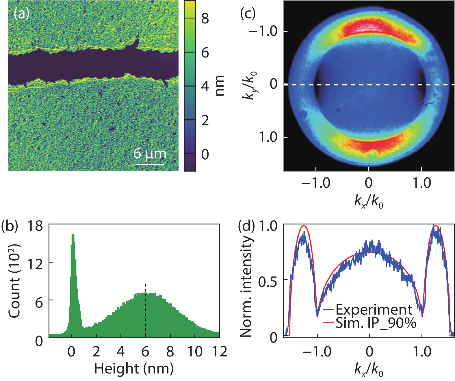
To characterize the film thickness and flatness, an area with a crack was scanned using atomic force microscopy, as shown in Fig. 3(a). The image mostly has the same contrast with noticeable scattered darker voids where no nanoplatelets cover the substrate. Similar voids are also noticeable in the results of recent studies where liquid surface assembly was used[2, 16]. The nanoplatelets on the acetonitrile surface prefers face-down orientation due to the attractive interaction of nanoplatelets ligands and the sub-phase liquids[2, 17, 26]. Edge-to-edge interaction is weak because there are also fewer ligands on the edge due to their thin thickness, which prevents these nanoplatelets to form a strongly connected and dense film. However, for most applications where multiple layers are needed, these voids can be covered by additional layers and would not be problematic. From the height histogram in Fig. 3(b), the average film thickness is 6 nm, which closely equals the total thickness of the nanoplatelets (1.5 nm) and two layers capping ligands (oleic acid of ~ 2 nm). Fig. 3(b) shows that there is a thickness distribution of 5.6 nm as calculated by the full width at half maximum. This variation partially due the scattered voids mentioned above, and partially due to nanoplatelets with edge-up orientation as have been observed in the TEM image in Fig. 2(c). The histogram does show a single peak centered at 6 nm that agrees well with the TEM characterization of a single-layer CdSe nanoplate film with dominant face-down orientation. We have measured the brighter stripes in Fig. 2(a) using AFM, and it reveals they are two layers with also the nanoplatelets having the face-down orientation.

Figure  3.  (Color online) (a) AFM image of a CdSe nanoplatelet monolayer film transferred on a cover glass. (b) Height histography of panel a, two peaks correspond to the bare glass and the height of the film. (c) Back focal plane image of the film. (d) Comparison between simulation and experimental BFP results along the dashed crossline in panel c.

Several studies have revealed that these nanoplatelets have pure in-plane dipoles[2, 4]. Back focal plane imaging (BFP) is a convenient method to characterizing the ensemble transition dipole distributions[2, 27]. In-plane dipole and out-plane dipole show very different image patterns in momentum space, and combined with simulation quantitative results can be drawn. Fig. 3(c) presents the BFP image of the monolayer CdSe film transferred on a cover glass. A typical feature from in-pane dipoles of two dark region at |kx| = k0 and ky = 0 can be clear seen. Quantitative simulation determines that the film has 90% in-plane dipole distribution (Fig. 3(d)), which is well in line with the TEM characterization. CdSe nanoplatelets have pure in-plane dipoles, and within the nanoplatelets plane the transition dipoles have no preferred direction[2]. Nanoplatelets with edge-up orientation have half in-plane and half out-plane transition dipoles. From the TEM analysis, we have calculated that 87% nanoplatelet have in-plane orientation, which have pure in-plane transition dipoles. In the rest, 13% of the nanoplatelets with edge-up configuration transition dipoles are oriented half in-plane and half out of the plane, and hence the total dipoles would have a 93.5% in-plane distribution that agrees well with optical characterization. Using the transferring methods, we have fabricated a sample with three layers of CdSe nanoplatelets films, as shown in Fig. 1(e). It gives the same BFP results as the monolayer as expected since each layer is similar.

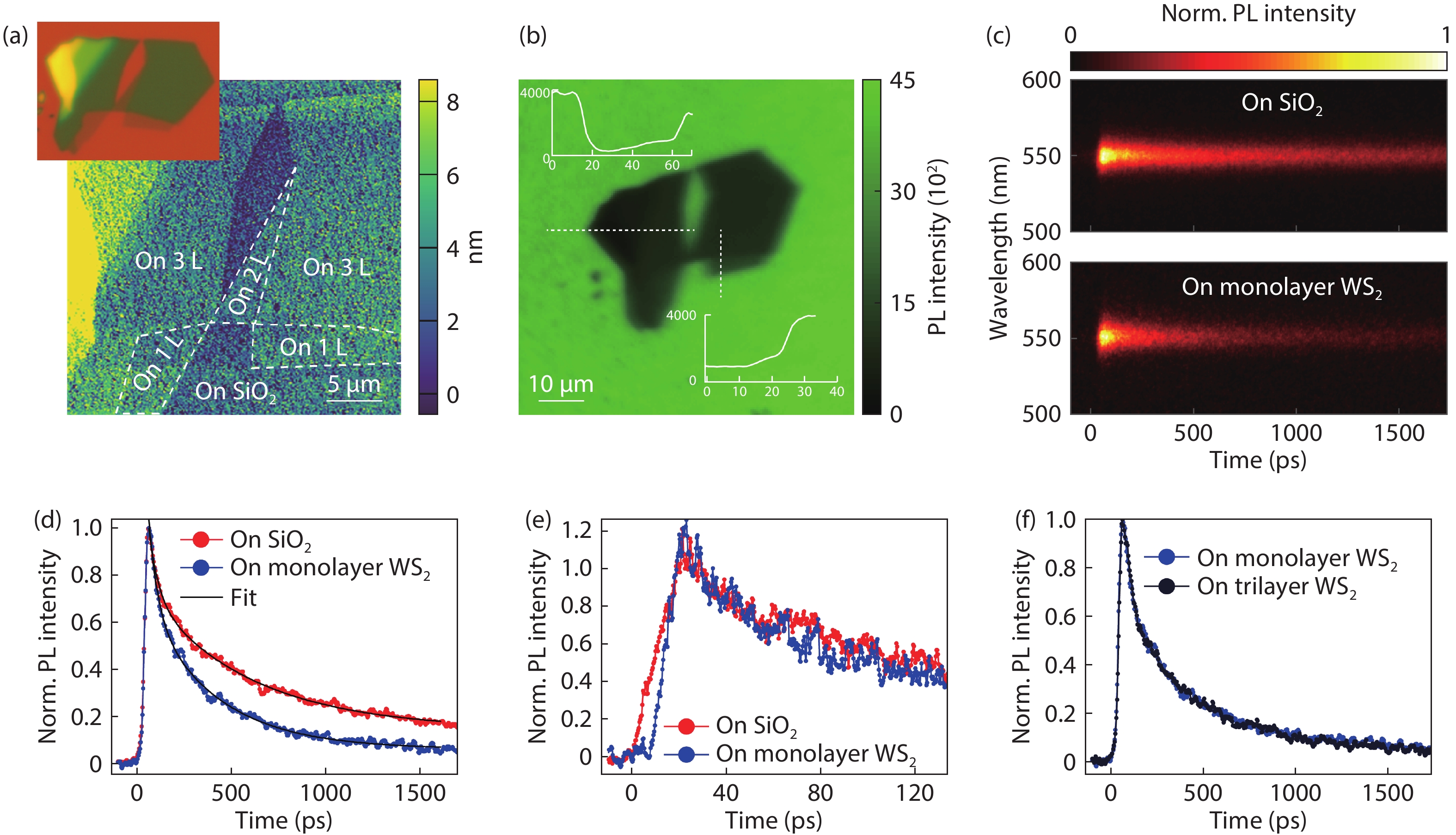
With the controlled nanoplatelet orientation and easily obtained films bigger than hundreds of micrometers, construction of hybrid heterostructures with other materials becomes much more convenient. Herein, we chose WS2 flakes as a targeted material as it is one of two-dimensional materials under intensive studies in recent years, and study energy transfer between these two types of two-dimensional materials. In Fig. 4(a), the up-left panel shows an optical microscopy image of a WS2 flakes consisting different layers, and down-right panel presents an AFM image of the constructed heterostructure, where the WS2 layer numbers are labeled. The WS2 layers were determined by the optical contrast and the thickness is measured by AFM.

Figure  4.  (Color online) (a) Up-left panel is an optical microscopy image of WS2 flakes on SiO2/Si, and down-right panel is an AFM image of single-layer CdSe nanoplatelets transferred on the WS2 flakes. (b) Wide field photoluminescence image of the CdSe film on/off the WS2 flakes, and the insets show the intensity change along the dashed white lines. (c) Time- and wavelength-resolved photoluminescence images measured by a streak camera. (d) Integrated intensity decay traces over the emission band in panel c, and biexponential functions are used to fit the decay traces. (e) Similar measurements as in panel c but with a shorter detection window and higher time resolution. (f) Comparison of photoluminescence decay of CdSe nanoplatelets on monolayer and trilayer WS2.

Fig. 4(b) presents a photoluminescence microscopy image (measured at 550 nm with a band width of 17 nm) of the hybrid heterostructure and the area around with pure single-layer CdSe nanoplatelet. It clearly shows that with WS2 flakes underneath the nanoplatelet film has much lower photoluminescence intensity seen as the darker area. Two insets show the intensity change along the dashed lines. We calculated that monolayer WS2 decreases the photoluminescence intensity of the nanoplatelets to 33% while triple-layer to 22% and the much thicker layer to 7%. This photoluminescence decrease is due to energy transfer from the CdSe nanoplatelet to WS2 flakes, since the WS2 flakes have a lower energy band gap. Direct charge carrier transfer can be excluded as these CdSe nanoplatelets have capping ligands of oleic acid of about 2 nm length.

The energy transfer rate in these hybrid heterostructures have been reported with a broad variation in literature[28-31]. Federspiel et al. reported 5.5 ns–1 energy transfer rate from CdSe/CdS/ZnS nanoplatelets to graphene. Taghipour et al. claimed an extremely high rate from CdSe nanoplatelets (emission peak at 510 nm) to monolayer MoS2 of 268 ns–1, however the ultrafast process reported in that work is within their instrument response function and the rate was extracted by multiexponential function fitting. By using a streak camera with a ps time-resolution, we can more directedly and accurately measure the energy transfer rate in a similar hybrid heterostructure of CdSe nanoplatelets (emission peak at 550 nm) and WS2 flakes.

Fig. 4(c) presents two photoluminescence decay images of the nanoplatelet film on bare substrates and on the monolayer WS2 region. Clear shortened decay can be seen. The total intensity decay traces over the emission band are shown in Fig. 4(d). A biexponential decay function can well fit the decay traces. The fitting extracted two components of with decay time of 53 ± 3 ps and 587 ± 14 ps on the bare substrate while 50 ± 3 ps and 380 ± 8 ps on monolayer WS2. The decay time of the faster component is the same, and from the change of the decay time of the slower component the energy transfer rate can be calculated as 4.3 ns–1 by Γ1τT=1τWS21τglass, where τWS2 and τglass are the decay time of the slower component on the corresponding substrate. The rising time in Fig. 4(d) is 47 ps. To check whether the instrument time resolution prevents us from observing an even faster energy transfer process, we used a setting in the streak camera with shorter time range and higher time resolution. As shown in Fig. 4(e), the signal rising time shortens to 15 ps, but no clear difference can be seen over the detection time-window of about 100 ps. The energy transfer rate in our hybrid system of 4.3 ns–1 is close to 5.5 ns–1 between CdSe/CdS/ZnS nanoplatelets and graphene[30]. By using a streak camera with a much higher time-resolution, we did not observe much faster energy transfer process.

Fig. 4(f) compares normalized decay traces of the nanoplatelets on monolayer and trilayer WS2 showing no noticeable difference in this time range. Though the trilayer WS2 quenches the steady state photoluminescence of CdSe nanoplatelets by 10% more (Fig. 4(b)), apparently it does not noticeably change the energy transfer rate in this heterostructure. It has been observed that thinner MoS2 acceptor layers lead to more efficient energy transfer from CdSe quantum dot donor, while graphene shows a contrary trend[29, 30]. In both cases, the thickness effect is more observable in a longer time scale. The different trends were due to the competition between screening and absorption of the acceptor layers[29-31].

We developed a PDMS-assisted transferring method that can conveniently pick up self-assembled CdSe nanoplatelets from acetonitrile surface and precisely transfer to a targeted substrate. Using the method, a hybrid heterostructure of CdSe nanoplatelets and WS2 flakes was constructed, in which the nanoplatelets have 90% in-plane orientation. By using a streak camera with ps time resolution, the energy transfer rate between the nanoplatelets and the WS2 flakes is accurately determined.

This project is supported by Beijing Natural Science Foundation (grant no. Z190005), the National Natural Science Foundation of China (grant nos. 61875002) and the National Key R&D Program of China (grant no. 2018YFA0306302).


[1]
Kovalenko M V, Manna L, Cabot A, et al. Prospects of nanoscience with nanocrystals. ACS Nano, 2015, 9, 1012 doi: 10.1021/nn506223h
[2]
Gao Y N, Weidman M C, Tisdale W A. CdSe nanoplatelet films with controlled orientation of their transition dipole moment. Nano Lett, 2017, 17, 3837 doi: 10.1021/acs.nanolett.7b01237
[3]
Ithurria S, Tessier M D, Mahler B, et al. Colloidal nanoplatelets with two-dimensional electronic structure. Nat Mater, 2011, 10, 936 doi: 10.1038/nmat3145
[4]
Scott R, Heckmann J, Prudnikau A V, et al. Directed emission of CdSe nanoplatelets originating from strongly anisotropic 2D electronic structure. Nat Nanotechnol, 2017, 12, 1155 doi: 10.1038/nnano.2017.177
[5]
Kim W D, Kim D, Yoon D E, et al. Pushing the efficiency envelope for semiconductor nanocrystal-based electroluminescence devices using anisotropic nanocrystals. Chem Mater, 2019, 31, 3066 doi: 10.1021/acs.chemmater.8b05366
[6]
Yang Z, Pelton M, Fedin I, et al. A room temperature continuous-wave nanolaser using colloidal quantum wells. Nat Commun, 2017, 8, 143 doi: 10.1038/s41467-017-00198-z
[7]
Grim J Q, Christodoulou S, Di Stasio F, et al. Continuous-wave biexciton lasing at room temperature using solution-processed quantum wells. Nat Nanotechnol, 2014, 9, 891 doi: 10.1038/nnano.2014.213
[8]
Giovanella U, Pasini M, Lorenzon M, et al. Efficient solution-processed nanoplatelet-based light-emitting diodes with high operational stability in air. Nano Lett, 2018, 18, 3441 doi: 10.1021/acs.nanolett.8b00456
[9]
Zhang F J, Wang S J, Wang L, et al. Super color purity green quantum dot light-emitting diodes fabricated by using CdSe/CdS nanoplatelets. Nanoscale, 2016, 8, 12182 doi: 10.1039/C6NR02922A
[10]
Boles M A, Engel M, Talapin D V. Self-assembly of colloidal nanocrystals: From intricate structures to functional materials. Chem Rev, 2016, 116, 11220 doi: 10.1021/acs.chemrev.6b00196
[11]
Li X, Lu Z L, Wang T. Self-assembly of semiconductor nanoparticles toward emergent behaviors on fluorescence. Nano Res, 2021, 14, 1233 doi: 10.1007/s12274-020-3140-y
[12]
Vanmaekelbergh D. Self-assembly of colloidal nanocrystals as route to novel classes of nanostructured materials. Nano Today, 2011, 6, 419 doi: 10.1016/j.nantod.2011.06.005
[13]
Dong A, Chen J, Vora P M, et al. Binary nanocrystal superlattice membranes self-assembled at the liquid-air interface. Nature, 2010, 466, 474 doi: 10.1038/nature09188
[14]
Abécassis B, Tessier M D, Davidson P, et al. Self-assembly of CdSe nanoplatelets into giant micrometer-scale needles emitting polarized light. Nano Lett, 2014, 14, 710 doi: 10.1021/nl4039746
[15]
Erdem O, Foroutan S, Gheshlaghi N, et al. Thickness-tunable self-assembled colloidal nanoplatelet films enable ultrathin optical gain media. Nano Lett, 2020, 20, 6459 doi: 10.1021/acs.nanolett.0c02153
[16]
Momper R, Zhang H, Chen S, et al. Kinetic control over self-assembly of semiconductor nanoplatelets. Nano Lett, 2020, 20, 4102 doi: 10.1021/acs.nanolett.9b05270
[17]
Erdem O, Gungor K, Guzelturk B, et al. Orientation-controlled nonradiative energy transfer to colloidal nanoplatelets: Engineering dipole orientation factor. Nano Lett, 2019, 19, 4297 doi: 10.1021/acs.nanolett.9b00681
[18]
Bai P, Hu A, Liu Y, et al. Printing and in situ assembly of CdSe/CdS nanoplatelets as uniform films with unity in-plane transition dipole moment. J Phys Chem Lett, 2020, 11, 4524 doi: 10.1021/acs.jpclett.0c00748
[19]
Özdemir O, Ramiro I, Gupta S, et al. High sensitivity hybrid PbS CQD-TMDC photodetectors up to 2 μm. ACS Photonics, 2019, 6, 2381 doi: 10.1021/acsphotonics.9b00870
[20]
Prins F, Kim D K, Cui J, et al. Direct patterning of colloidal quantum-dot thin films for enhanced and spectrally selective out-coupling of emission. Nano Lett, 2017, 17, 1319 doi: 10.1021/acs.nanolett.6b03212
[21]
He Z, Chen B, Hua Y, et al. CMOS compatible high-performance nanolasing based on perovskite-SiN hybrid integration. Adv Opt Mater, 2020, 8, 2000453 doi: 10.1002/adom.202000453
[22]
Prasai D, Klots A R, Newaz A, et al. Electrical control of near-field energy transfer between quantum dots and two-dimensional semiconductors. Nano Lett, 2015, 15, 4374 doi: 10.1021/acs.nanolett.5b00514
[23]
Dutta A, Medda A, Bera R, et al. Hybrid nanostructures of 2D CdSe nanoplatelets for high-performance photodetector using charge transfer process. ACS Appl Nano Mater, 2020, 3, 4717 doi: 10.1021/acsanm.0c00728
[24]
Rowland C E, Fedin I, Zhang H, et al. Picosecond energy transfer and multiexciton transfer outpaces Auger recombination in binary CdSe nanoplatelet solids. Nat Mater, 2015, 14, 484 doi: 10.1038/nmat4231
[25]
She C X, Fedin I, Dolzhnikov D S, et al. Low-threshold stimulated emission using colloidal quantum wells. Nano Lett, 2014, 14, 2772 doi: 10.1021/nl500775p
[26]
Paik T, Ko D K, Gordon T R, et al. Studies of liquid crystalline self-assembly of GdF3 nanoplates by in-plane, out-of-plane SAXS. ACS Nano, 2011, 5, 8322 doi: 10.1021/nn203049t
[27]
Schuller J A, Karaveli S, Schiros T, et al. Orientation of luminescent excitons in layered nanomaterials. Nat Nanotechnol, 2013, 8, 271 doi: 10.1038/nnano.2013.20
[28]
Taghipour N, Hernandez Martinez P L, Ozden A, et al. Near-unity efficiency energy transfer from colloidal semiconductor quantum wells of CdSe/CdS nanoplatelets to a monolayer of MoS2. ACS Nano, 2018, 12, 8547 doi: 10.1021/acsnano.8b04119
[29]
Prins F, Goodman A J, Tisdale W A. Reduced dielectric screening and enhanced energy transfer in single- and few-layer MoS2. Nano Lett, 2014, 14, 6087 doi: 10.1021/nl5019386
[30]
Raja A, Montoya−Castillo A, Zultak J, et al. Energy transfer from quantum dots to graphene and MoS2: The role of absorption and screening in two-dimensional materials. Nano Lett, 2016, 16, 2328 doi: 10.1021/acs.nanolett.5b05012
[31]
Liu H, Wang T, Wang C, et al. Exciton radiative recombination dynamics and nonradiative energy transfer in two-dimensional transition-metal dichalcogenides. J Phys Chem C, 2019, 123, 10087 doi: 10.1021/acs.jpcc.8b12179
Fig. 1.  (Color online) (a) Absorption and photoluminescence spectra of the CdSe nanoplatelets. (b) Transmission electron microscopy (TEM) image of the nanoplatelets. (c) Schematic of PDMS assisted transferring method. (d) A bright-field microscopy image of a single layer of the CdSe nanoplatelet film on a SiO2/Si substrate with WS2 flakes. (e) Photoluminescence microscopy image of CdSe films with one, two and three layers of nanoplatelets.

Fig. 2.  (Color online) (a) Photoluminescence microscopy image of a layer CdSe film transferred on a cover glass. (b, c) TEM images of a film on a SiN substrate: (b) panel (lower magnification) shows the homogeneity, and several voids are pointed out by dashed circles; (c) panel (higher magnification) shows that nanoplatelets have dominant in-plane orientation of about 90%, and the inset displayed a zoomed-in portion with nanoplatelets in edge-up (circled in dashed lines) and face-down orientations.

Fig. 3.  (Color online) (a) AFM image of a CdSe nanoplatelet monolayer film transferred on a cover glass. (b) Height histography of panel a, two peaks correspond to the bare glass and the height of the film. (c) Back focal plane image of the film. (d) Comparison between simulation and experimental BFP results along the dashed crossline in panel c.

Fig. 4.  (Color online) (a) Up-left panel is an optical microscopy image of WS2 flakes on SiO2/Si, and down-right panel is an AFM image of single-layer CdSe nanoplatelets transferred on the WS2 flakes. (b) Wide field photoluminescence image of the CdSe film on/off the WS2 flakes, and the insets show the intensity change along the dashed white lines. (c) Time- and wavelength-resolved photoluminescence images measured by a streak camera. (d) Integrated intensity decay traces over the emission band in panel c, and biexponential functions are used to fit the decay traces. (e) Similar measurements as in panel c but with a shorter detection window and higher time resolution. (f) Comparison of photoluminescence decay of CdSe nanoplatelets on monolayer and trilayer WS2.

[1]
Kovalenko M V, Manna L, Cabot A, et al. Prospects of nanoscience with nanocrystals. ACS Nano, 2015, 9, 1012 doi: 10.1021/nn506223h
[2]
Gao Y N, Weidman M C, Tisdale W A. CdSe nanoplatelet films with controlled orientation of their transition dipole moment. Nano Lett, 2017, 17, 3837 doi: 10.1021/acs.nanolett.7b01237
[3]
Ithurria S, Tessier M D, Mahler B, et al. Colloidal nanoplatelets with two-dimensional electronic structure. Nat Mater, 2011, 10, 936 doi: 10.1038/nmat3145
[4]
Scott R, Heckmann J, Prudnikau A V, et al. Directed emission of CdSe nanoplatelets originating from strongly anisotropic 2D electronic structure. Nat Nanotechnol, 2017, 12, 1155 doi: 10.1038/nnano.2017.177
[5]
Kim W D, Kim D, Yoon D E, et al. Pushing the efficiency envelope for semiconductor nanocrystal-based electroluminescence devices using anisotropic nanocrystals. Chem Mater, 2019, 31, 3066 doi: 10.1021/acs.chemmater.8b05366
[6]
Yang Z, Pelton M, Fedin I, et al. A room temperature continuous-wave nanolaser using colloidal quantum wells. Nat Commun, 2017, 8, 143 doi: 10.1038/s41467-017-00198-z
[7]
Grim J Q, Christodoulou S, Di Stasio F, et al. Continuous-wave biexciton lasing at room temperature using solution-processed quantum wells. Nat Nanotechnol, 2014, 9, 891 doi: 10.1038/nnano.2014.213
[8]
Giovanella U, Pasini M, Lorenzon M, et al. Efficient solution-processed nanoplatelet-based light-emitting diodes with high operational stability in air. Nano Lett, 2018, 18, 3441 doi: 10.1021/acs.nanolett.8b00456
[9]
Zhang F J, Wang S J, Wang L, et al. Super color purity green quantum dot light-emitting diodes fabricated by using CdSe/CdS nanoplatelets. Nanoscale, 2016, 8, 12182 doi: 10.1039/C6NR02922A
[10]
Boles M A, Engel M, Talapin D V. Self-assembly of colloidal nanocrystals: From intricate structures to functional materials. Chem Rev, 2016, 116, 11220 doi: 10.1021/acs.chemrev.6b00196
[11]
Li X, Lu Z L, Wang T. Self-assembly of semiconductor nanoparticles toward emergent behaviors on fluorescence. Nano Res, 2021, 14, 1233 doi: 10.1007/s12274-020-3140-y
[12]
Vanmaekelbergh D. Self-assembly of colloidal nanocrystals as route to novel classes of nanostructured materials. Nano Today, 2011, 6, 419 doi: 10.1016/j.nantod.2011.06.005
[13]
Dong A, Chen J, Vora P M, et al. Binary nanocrystal superlattice membranes self-assembled at the liquid-air interface. Nature, 2010, 466, 474 doi: 10.1038/nature09188
[14]
Abécassis B, Tessier M D, Davidson P, et al. Self-assembly of CdSe nanoplatelets into giant micrometer-scale needles emitting polarized light. Nano Lett, 2014, 14, 710 doi: 10.1021/nl4039746
[15]
Erdem O, Foroutan S, Gheshlaghi N, et al. Thickness-tunable self-assembled colloidal nanoplatelet films enable ultrathin optical gain media. Nano Lett, 2020, 20, 6459 doi: 10.1021/acs.nanolett.0c02153
[16]
Momper R, Zhang H, Chen S, et al. Kinetic control over self-assembly of semiconductor nanoplatelets. Nano Lett, 2020, 20, 4102 doi: 10.1021/acs.nanolett.9b05270
[17]
Erdem O, Gungor K, Guzelturk B, et al. Orientation-controlled nonradiative energy transfer to colloidal nanoplatelets: Engineering dipole orientation factor. Nano Lett, 2019, 19, 4297 doi: 10.1021/acs.nanolett.9b00681
[18]
Bai P, Hu A, Liu Y, et al. Printing and in situ assembly of CdSe/CdS nanoplatelets as uniform films with unity in-plane transition dipole moment. J Phys Chem Lett, 2020, 11, 4524 doi: 10.1021/acs.jpclett.0c00748
[19]
Özdemir O, Ramiro I, Gupta S, et al. High sensitivity hybrid PbS CQD-TMDC photodetectors up to 2 μm. ACS Photonics, 2019, 6, 2381 doi: 10.1021/acsphotonics.9b00870
[20]
Prins F, Kim D K, Cui J, et al. Direct patterning of colloidal quantum-dot thin films for enhanced and spectrally selective out-coupling of emission. Nano Lett, 2017, 17, 1319 doi: 10.1021/acs.nanolett.6b03212
[21]
He Z, Chen B, Hua Y, et al. CMOS compatible high-performance nanolasing based on perovskite-SiN hybrid integration. Adv Opt Mater, 2020, 8, 2000453 doi: 10.1002/adom.202000453
[22]
Prasai D, Klots A R, Newaz A, et al. Electrical control of near-field energy transfer between quantum dots and two-dimensional semiconductors. Nano Lett, 2015, 15, 4374 doi: 10.1021/acs.nanolett.5b00514
[23]
Dutta A, Medda A, Bera R, et al. Hybrid nanostructures of 2D CdSe nanoplatelets for high-performance photodetector using charge transfer process. ACS Appl Nano Mater, 2020, 3, 4717 doi: 10.1021/acsanm.0c00728
[24]
Rowland C E, Fedin I, Zhang H, et al. Picosecond energy transfer and multiexciton transfer outpaces Auger recombination in binary CdSe nanoplatelet solids. Nat Mater, 2015, 14, 484 doi: 10.1038/nmat4231
[25]
She C X, Fedin I, Dolzhnikov D S, et al. Low-threshold stimulated emission using colloidal quantum wells. Nano Lett, 2014, 14, 2772 doi: 10.1021/nl500775p
[26]
Paik T, Ko D K, Gordon T R, et al. Studies of liquid crystalline self-assembly of GdF3 nanoplates by in-plane, out-of-plane SAXS. ACS Nano, 2011, 5, 8322 doi: 10.1021/nn203049t
[27]
Schuller J A, Karaveli S, Schiros T, et al. Orientation of luminescent excitons in layered nanomaterials. Nat Nanotechnol, 2013, 8, 271 doi: 10.1038/nnano.2013.20
[28]
Taghipour N, Hernandez Martinez P L, Ozden A, et al. Near-unity efficiency energy transfer from colloidal semiconductor quantum wells of CdSe/CdS nanoplatelets to a monolayer of MoS2. ACS Nano, 2018, 12, 8547 doi: 10.1021/acsnano.8b04119
[29]
Prins F, Goodman A J, Tisdale W A. Reduced dielectric screening and enhanced energy transfer in single- and few-layer MoS2. Nano Lett, 2014, 14, 6087 doi: 10.1021/nl5019386
[30]
Raja A, Montoya−Castillo A, Zultak J, et al. Energy transfer from quantum dots to graphene and MoS2: The role of absorption and screening in two-dimensional materials. Nano Lett, 2016, 16, 2328 doi: 10.1021/acs.nanolett.5b05012
[31]
Liu H, Wang T, Wang C, et al. Exciton radiative recombination dynamics and nonradiative energy transfer in two-dimensional transition-metal dichalcogenides. J Phys Chem C, 2019, 123, 10087 doi: 10.1021/acs.jpcc.8b12179
1

Perylene diimide self-assembly: From electronic structural modulation to photocatalytic applications

Weiqin Wei, Shuxin Ouyang, Tierui Zhang

Journal of Semiconductors, 2020, 41(9): 091708. doi: 10.1088/1674-4926/41/9/091708

2

Engineering in-plane silicon nanowire springs for highly stretchable electronics

Zhaoguo Xue, Taige Dong, Zhimin Zhu, Yaolong Zhao, Ying Sun, et al.

Journal of Semiconductors, 2018, 39(1): 011001. doi: 10.1088/1674-4926/39/1/011001

3

The electronic and magnetic properties of wurtzite Mn:CdS, Cr:CdS and Mn:Cr:CdS: first principles calculations

Azeem Nabi, Zarmeena Akhtar, Tahir Iqbal, Atif Ali, Arshad Javid, et al.

Journal of Semiconductors, 2017, 38(7): 073001. doi: 10.1088/1674-4926/38/7/073001

4

Colloidal synthesis and characterization of Cu2ZnSnS4 nanoplates

S. Ananthakumar, J. Ram Kumar, S. Moorthy Babu

Journal of Semiconductors, 2017, 38(3): 033007. doi: 10.1088/1674-4926/38/3/033007

5

Recent advances in preparation,properties and device applications of two-dimensional h-BN and its vertical heterostructures

Huihui Yang, Feng Gao, Mingjin Dai, Dechang Jia, Yu Zhou, et al.

Journal of Semiconductors, 2017, 38(3): 031004. doi: 10.1088/1674-4926/38/3/031004

6

Variable range hopping conduction in n-CdSe samples at very low temperature

M Errai, A El Kaaouachi, H El Idrissi

Journal of Semiconductors, 2015, 36(12): 122001. doi: 10.1088/1674-4926/36/12/122001

7

Effect of the side-Ohmic contact processing on the polarization Coulomb field scattering in AlN/GaN heterostructure field-effect transistors

Jingtao Zhao, Zhaojun Lin, Chongbiao Luan, Ming Yang, Yang Zhou, et al.

Journal of Semiconductors, 2014, 35(12): 124003. doi: 10.1088/1674-4926/35/12/124003

8

Effect of band gap energy on the electrical conductivity in doped ZnO thin film

Said Benramache, Okba Belahssen, Hachemi Ben Temam

Journal of Semiconductors, 2014, 35(7): 073001. doi: 10.1088/1674-4926/35/7/073001

9

The influence of the channel electric field distribution on the polarization Coulomb field scattering in AlN/GaN heterostructure field-effect transistors

Yingxia Yu, Zhaojun Lin, Yuanjie Lü, Zhihong Feng, Chongbiao Luan, et al.

Journal of Semiconductors, 2014, 35(12): 124007. doi: 10.1088/1674-4926/35/12/124007

10

Unstrained InAlN/GaN heterostructures grown on sapphire substrates by MOCVD

Bo Liu, Jiayun Yin, Yuanjie Lü, Shaobo Dun, Xiongwen Zhang, et al.

Journal of Semiconductors, 2014, 35(11): 113005. doi: 10.1088/1674-4926/35/11/113005

11

Transition Gibbs free energy level cross section and formulation of carrier SRH recombination rate

Ken K. Chin

Journal of Semiconductors, 2013, 34(12): 122001. doi: 10.1088/1674-4926/34/12/122001

12

Fabrication and characterization of a low frequency electromagnetic energy harvester

Abu Riduan Md. Foisal, Gwiy-Sang Chung

Journal of Semiconductors, 2012, 33(7): 074001. doi: 10.1088/1674-4926/33/7/074001

13

Radiation effect on the optical and electrical properties of CdSe(In)/p-Si heterojunction photovoltaic solar cells

M. Ashry, S. Fares

Journal of Semiconductors, 2012, 33(10): 102001. doi: 10.1088/1674-4926/33/10/102001

14

Mathematical modeling of nanoscale MOS capacitance in the presence of depletion and energy quantization in a poly-silicon gate

Amit Chaudhry, J. N. Roy

Journal of Semiconductors, 2010, 31(11): 114001. doi: 10.1088/1674-4926/31/11/114001

15

Influence of Ni Schottky contact thickness on two-dimensional electron-gas sheet carrier concentration of strained Al0.3Ga0.7N/GaN heterostructures

Zhao Jianzhi, Lin Zhaojun, Lü Yuanjie, Corrigan Timothy D, Meng Lingguo, et al.

Journal of Semiconductors, 2010, 31(8): 084007. doi: 10.1088/1674-4926/31/8/084007

16

Synthesis and Properties of bis(2-Hydroxy-3-Methoxy Benzaldehyde) Schiff Base and Its Zinc (Ⅱ) Complex

Chen Liuqing, Xu Huixia, Wang Hua, Hou Lixin, Ma Chen, et al.

Chinese Journal of Semiconductors , 2007, 28(S1): 352-356.

17

Photoluminescence Characterization of HfON∶Tb Films with Sputtering

Jiang Ran, Xie Erqing, Jia Changwen, Lin Hongfeng, Pan Xiaojun, et al.

Chinese Journal of Semiconductors , 2006, 27(S1): 169-171.

18

1.3μm InGaAs/InAs/GaAs Self-Assembled Quantum Dot Laser Diode Grown by Molecular Beam Epitaxy

Niu Zhichuan, Ni Haiqiao, Fang Zhidan, Gong Zheng, Zhang Shiyong, et al.

Chinese Journal of Semiconductors , 2006, 27(3): 482-488.

19

Energy Transfer Probability Between Host and Guest in Doped Organic Electrophosphorescent Devices

Li Hongjian, Ouyang Jun, Dai Guozhang, Dai Xiaoyu, Pan Yanzhi, et al.

Chinese Journal of Semiconductors , 2006, 27(4): 674-678.

20

Electronic Structure and optical Properties of Wurtzite CdSe Ouantum Ellipsoid

Xia Jianbai, Li Xinzheng

Chinese Journal of Semiconductors , 2003, 24(S1): 34-37.

1. Nisham Rosly, H., Doroody, C., Harif, M.N. et al. Optoelectrical Properties of Treated CdSe Thin Films with Variations in Indium Chloride Concentration. Materials, 2023, 16(11): 4108. doi:10.3390/ma16114108
2. He, Y.-F., Yang, D.-R., Pi, X.-D. Enhanced PdSe2/Si heterojunction photodetector by Al2O3 layer | [氧化铝增强的 PdSe2/Si 异质结光电探测器]. Zhejiang Daxue Xuebao (Gongxue Ban)/Journal of Zhejiang University (Engineering Science), 2023, 57(1): 190-199. doi:10.3785/j.issn.1008-973X.2023.01.019
3. Ke, Y., Cen, Y., Qi, D. et al. Two-Dimensional Materials Photodetectors for Optical Communications | [基 于 二 维 材 料 的 光 通 信 波 段 光 电 探 测 器]. Zhongguo Jiguang/Chinese Journal of Lasers, 2023, 50(1): 0113008. doi:10.3788/CJL221133
4. Asaithambi, A., Kazemi Tofighi, N., Curreli, N. et al. Generation of Free Carriers in MoSe2 Monolayers Via Energy Transfer from CsPbBr3 Nanocrystals. Advanced Optical Materials, 2022, 10(14): 2200638. doi:10.1002/adom.202200638
5. Zhou, Y., Han, L., Song, Q. et al. Hybrid 1D/2D heterostructure with electronic structure engineering toward high-sensitivity and polarization-dependent photodetector | [混合1D/2D异质结构耦合电子结构工程用于高灵敏度和偏振依赖的光电探测器]. Science China Materials, 2022, 65(3): 732-740. doi:10.1007/s40843-021-1847-7
  • Search

    Advanced Search >>

    GET CITATION

    Zeguo Song, Yunkun Wang, Yunke Zhu, Peng Bai, An Hu, Yunan Gao. Targeted transfer of self-assembled CdSe nanoplatelet film onto WS2 flakes to construct hybrid heterostructures[J]. Journal of Semiconductors, 2021, 42(8): 082901. doi: 10.1088/1674-4926/42/8/082901
    Z G Song, Y K Wang, Y K Zhu, P Bai, A Hu, Y N Gao, Targeted transfer of self-assembled CdSe nanoplatelet film onto WS2 flakes to construct hybrid heterostructures[J]. J. Semicond., 2021, 42(8): 082901. doi: 10.1088/1674-4926/42/8/082901.
    shu

    Export: BibTex EndNote

    Article Metrics

    Article views: 2661 Times PDF downloads: 73 Times Cited by: 5 Times

    History

    Received: 28 February 2021 Revised: 29 March 2021 Online: Accepted Manuscript: 27 April 2021Uncorrected proof: 14 May 2021Published: 01 August 2021

    Catalog

      Email This Article

      User name:
      Email:*请输入正确邮箱
      Code:*验证码错误
      Zeguo Song, Yunkun Wang, Yunke Zhu, Peng Bai, An Hu, Yunan Gao. Targeted transfer of self-assembled CdSe nanoplatelet film onto WS2 flakes to construct hybrid heterostructures[J]. Journal of Semiconductors, 2021, 42(8): 082901. doi: 10.1088/1674-4926/42/8/082901 ****Z G Song, Y K Wang, Y K Zhu, P Bai, A Hu, Y N Gao, Targeted transfer of self-assembled CdSe nanoplatelet film onto WS2 flakes to construct hybrid heterostructures[J]. J. Semicond., 2021, 42(8): 082901. doi: 10.1088/1674-4926/42/8/082901.
      Citation:
      Zeguo Song, Yunkun Wang, Yunke Zhu, Peng Bai, An Hu, Yunan Gao. Targeted transfer of self-assembled CdSe nanoplatelet film onto WS2 flakes to construct hybrid heterostructures[J]. Journal of Semiconductors, 2021, 42(8): 082901. doi: 10.1088/1674-4926/42/8/082901 ****
      Z G Song, Y K Wang, Y K Zhu, P Bai, A Hu, Y N Gao, Targeted transfer of self-assembled CdSe nanoplatelet film onto WS2 flakes to construct hybrid heterostructures[J]. J. Semicond., 2021, 42(8): 082901. doi: 10.1088/1674-4926/42/8/082901.

      Targeted transfer of self-assembled CdSe nanoplatelet film onto WS2 flakes to construct hybrid heterostructures

      DOI: 10.1088/1674-4926/42/8/082901
      More Information
      • Zeguo Song:received his B.S. degree in Physics (2018) at Shanghai University. He is currently pursuing his M.S. degree at School of Physics, Peking University. His current work focuses on study of optical properties of CdSe nanoplatelets
      • Yunan Gao:received his PhD from Delft University of Technology at 2012. In 2017 he joined School of Physics Peking University as an assistant professor. His research focuses on synthesis, self-assembly and optical property studies of colloidal semiconductor nanocrystals
      • Corresponding author: gyn@pku.edu.cn
      • Received Date: 2021-02-28
      • Revised Date: 2021-03-29
      • Published Date: 2021-08-10

      Catalog

        /

        DownLoad:  Full-Size Img  PowerPoint
        Return
        Return