ARTICLES

Synthesis and electromagnetic transport of large-area 2D WTe2 thin film

Yumeng Zhang1, 2, Zhejia Wang3, 4, Jiaheng Feng3, 4, Shuaiqiang Ming1, 3, Furong Qu1, 2, , Yang Xia1, 2, Meng He1, Zhimin Hu1, 2 and Jing Wang5

+ Author Affiliations

 Corresponding author: Furong Qu, qufurong@ime.ac.cn

PDF

Turn off MathJax

Abstract: Tungsten telluride thin films were successfully prepared on monocrystal sapphire substrates by using atomic layer deposition and chemical vapor deposition technology, and the effects of different tellurization temperatures on the properties of tungsten telluride films were investigated. The growth rate, crystal structure and composition of the film samples were characterized and analyzed by using scanning electron microscope, Raman spectroscopy and X-ray photoelectron spectroscopy. The results showed that tungsten telluride thin films with good crystal orientation in (001) were obtained at telluride temperature of 550 °C. When the telluride temperature reached 570 °C, the tungsten telluride began to decompose and unsaturated magnetoresistance was found.

Key words: atomic layer deposition (ALD)chemical vapor deposition (CVD)telluride temperatureWTe2 thin film


[1]
Qi X L, Zhang S C. Topological insulators and superconductors. Rev Mod Phys, 2011, 83, 1057 doi: 10.1103/RevModPhys.83.1057
[2]
Ghosh B, Gupta A, Bishnoi B. Effects of defects on the electronic properties of WTe2 armchair nanoribbons. J Semicond, 2014, 35, 113002 doi: 10.1088/1674-4926/35/11/113002
[3]
Zhou Z Q, Cui Y, Tan P H, et al. Optical and electrical properties of two-dimensional anisotropic materials. J Semicond, 2019, 40, 061001 doi: 10.1088/1674-4926/40/6/061001
[4]
Zhang P, Zhang Y W, Wei Y, et al. Contact engineering for two-dimensional semiconductors. J Semicond, 2020, 41, 071901 doi: 10.1088/1674-4926/41/7/071901
[5]
Bernevig B A, Hughes T L, Zhang S C. Quantum spin Hall effect and topological phase transition in HgTe quantum wells. Science, 2006, 314, 1757 doi: 10.1126/science.1133734
[6]
König M, Wiedmann S, Brüne C, et al. Quantum spin hall insulator state in HgTe quantum wells. Science, 2007, 318, 766 doi: 10.1126/science.1148047
[7]
Qian X F, Liu J W, Fu L, et al. Quantum spin Hall effect in two-dimensional transition metal dichalcogenides. Science, 2014, 346, 1344 doi: 10.1126/science.1256815
[8]
Liu C C, Feng W X, Yao Y G. Quantum spin Hall effect in silicene and two-dimensional germanium. Phys Rev Lett, 2011, 107, 076802 doi: 10.1103/PhysRevLett.107.076802
[9]
Xu Y, Yan B H, Zhang H J, et al. Large-gap quantum spin hall insulators in tin films. Phys Rev Lett, 2013, 111, 136804 doi: 10.1103/PhysRevLett.111.136804
[10]
Ali M N, Xiong J, Flynn S, et al. Large, non-saturating magnetoresistance in WTe2. Nature, 2014, 514, 205 doi: 10.1038/nature13763
[11]
Luo Y K, Li H, Dai Y M, et al. Hall effect in the extremely large magnetoresistance semimetal WTe2. Appl Phys Lett, 2015, 107, 182411 doi: 10.1063/1.4935240
[12]
Song Y, Zhang Q, Mi W B, et al. Valley polarization and p-/n-type doping of monolayer WTe2 on top of Fe3O4(111). Phys Chem Chem Phys, 2016, 18, 15039 doi: 10.1039/C6CP01986B
[13]
Zhu Z W, Lin X, Liu J, et al. Quantum oscillations, thermoelectric coefficients, and the Fermi surface of semimetallic WTe2. Phys Rev Lett, 2015, 114, 176601 doi: 10.1103/PhysRevLett.114.176601
[14]
Jiang J, Tang F, Pan X C, et al. Signature of strong spin-orbital coupling in the large nonsaturating magnetoresistance material WTe2. Phys Rev Lett, 2015, 115, 166601 doi: 10.1103/PhysRevLett.115.166601
[15]
Fei Z Y, Palomaki T, Wu S F, et al. Edge conduction in monolayer WTe2. Nat Phys, 2017, 13, 677 doi: 10.1038/nphys4091
[16]
Wu S F, Fatemi V, Gibson Q D, et al. Observation of the quantum spin Hall effect up to 100 kelvin in a monolayer crystal. Science, 2018, 359, 76 doi: 10.1126/science.aan6003
[17]
Song Y H, Jia Z Y, Zhang D Q, et al. Observation of Coulomb gap in the quantum spin Hall candidate single-layer 1T’-WTe2. Nat Commun, 2018, 9, 4071 doi: 10.1038/s41467-018-06635-x
[18]
Jia Z Y, Song Y H, Li X B, et al. Direct visualization of a two-dimensional topological insulator in the single-layer 1T'-WTe2. Phys Rev B, 2017, 96, 041108 doi: 10.1103/PhysRevB.96.041108
[19]
Li J, Cheng S, Liu Z X, et al. Centimeter-scale, large-area, few-layer 1T'-WTe2 films by chemical vapor deposition and its long-term stability in ambient condition. J Phys Chem C, 2018, 122, 7005 doi: 10.1021/acs.jpcc.8b00679
[20]
Jiang Y C, Gao J, Wang L. Raman fingerprint for semi-metal WTe2 evolving from bulk to monolayer. Sci Rep, 2016, 6, 19624 doi: 10.1038/srep19624
[21]
Zhou J D, Liu F C, Lin J H, et al. 2D materials: Large-area and high-quality 2D transition metal telluride. Adv Mater, 2017, 29, 1603471 doi: 10.1002/adma.201603471
[22]
Zhou Y, Jang H, Woods J M, et al. Direct synthesis of large-scale WTe2 thin films with low thermal conductivity. Adv Funct Mater, 2017, 27, 1605928 doi: 10.1002/adfm.201605928
[23]
Aslan T, Mtsuko D, Coleman C, et al. Observation of Shubnikov de Haas and aharanov-bohm oscillations in silicon nanowires. arXiv: 1504.02325, 2015
[24]
Wang Y, Wang X, Xu Y, et al. Simultaneous synthesis of WO3– x quantum dots and bundle-like nanowires using a one-pot template-free solvothermal strategy and their versatile applications. Small, 2017, 11, 1310 doi: 10.1002/smll.201603689
[25]
Lu W, Zhang Y D, Zhu Z S, et al. Thin tungsten telluride layer preparation by thermal annealing. Nanotechnology, 2016, 27, 414006 doi: 10.1088/0957-4484/27/41/414006
[26]
Naylor C H, Parkin W M, Gao Z L, et al. Large-area synthesis of high-quality monolayer 1T'-WTe2 flakes. 2D Mater, 2017, 4, 021008 doi: 10.1088/2053-1583/aa5921
[27]
Shi S Y, Li J, Hsu C, et al. Observation of the out-of-plane polarized spin current from CVD grown WTe2. Adv Quantum Tech, 2021, 4, 2100038 doi: 10.1002/qute.202100038
[28]
Chen K, Chen Z, Wan X, et al. A simple method for synthesis of high-quality millimeter-scale 1T' transition-metal telluride and near-field nanooptical properties. Adv Mater, 2017, 29, 1700704 doi: 10.1002/adma.201700704
[29]
Mleczko M J, Xu R L, Okabe K, et al. High Current density and low thermal conductivity of atomically thin semimetallic WTe2. ACS Nano, 2016, 10, 7507 doi: 10.1021/acsnano.6b02368
[30]
Giri A, Yang H, Jang W, et al. Synthesis of atomically thin transition metal ditelluride films by rapid chemical transformation in solution phase. Chem Mater, 2018, 30, 2463 doi: 10.1021/acs.chemmater.8b00684
[31]
Cai P L, Hu J, He L P, et al. Drastic pressure effect on the extremely large magnetoresistance in WTe2: Quantum oscillation study. Phys Rev Lett, 2015, 115, 057202 doi: 10.1103/PhysRevLett.115.057202
[32]
Lv Y Y, Zhang B B, Li X, et al. Dramatically decreased magnetoresistance in non-stoichiometric WTe2 crystals. Sci Rep, 2016, 6, 26903 doi: 10.1038/srep26903
[33]
Pletikosić I, Ali M N, Fedorov A V, et al. Electronic structure basis for the extraordinary magnetoresistance in WTe2. Phys Rev Lett, 2014, 113, 216601 doi: 10.1103/PhysRevLett.113.216601
Fig. 1.  (Color online) (a) Schematic diagram of ALD device. (b) Schematic diagram of CVD device.

Fig. 2.  (Color online) (a) SEM image of cross section of tungsten thin film. (b) The XPS pattern of tungsten thin film. (c) The photo of tungsten film.

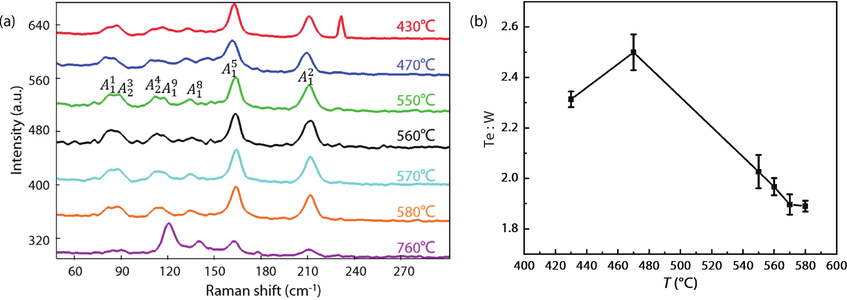
Fig. 3.  (Color online) (a) Raman spectrum at different telluride temperatures. (b) Te : W ratio-temperature curves in EDS results

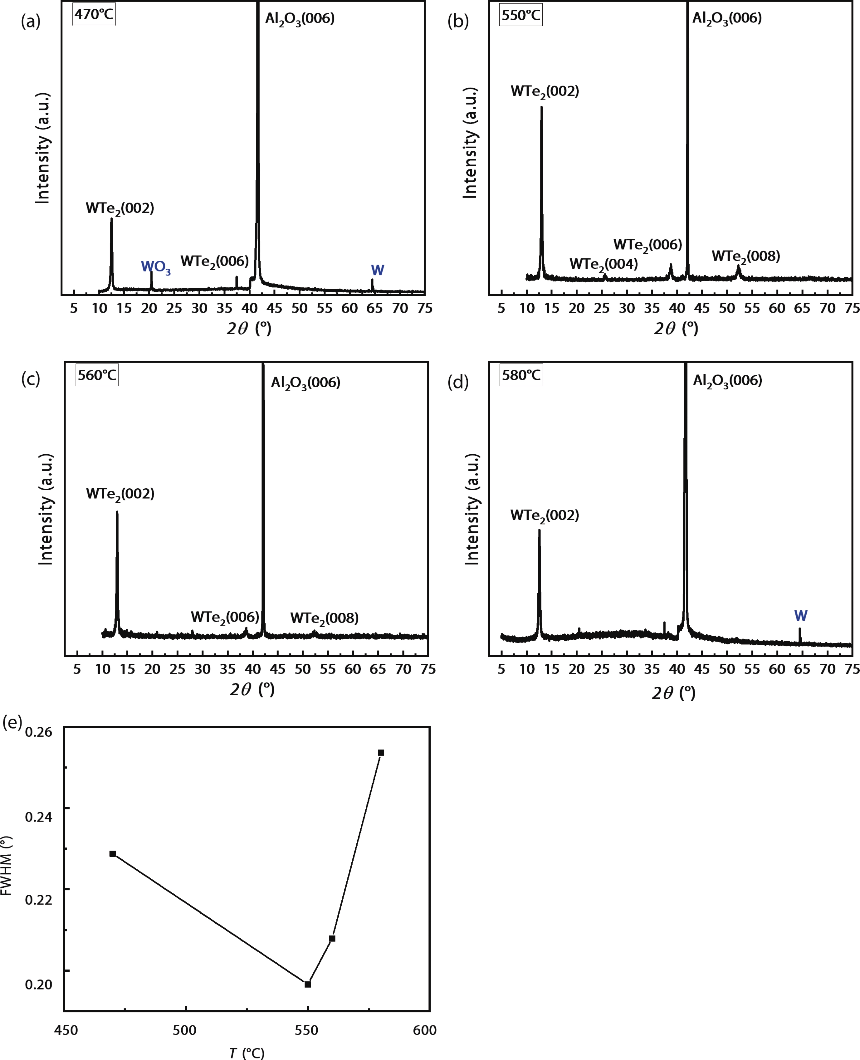
Fig. 4.  (a–d) XRD curves of telluride temperature at 470, 550, 560 and 580 °C. (e) FWHM of WTe2(002) at 470, 550, 560 and 580 °C.

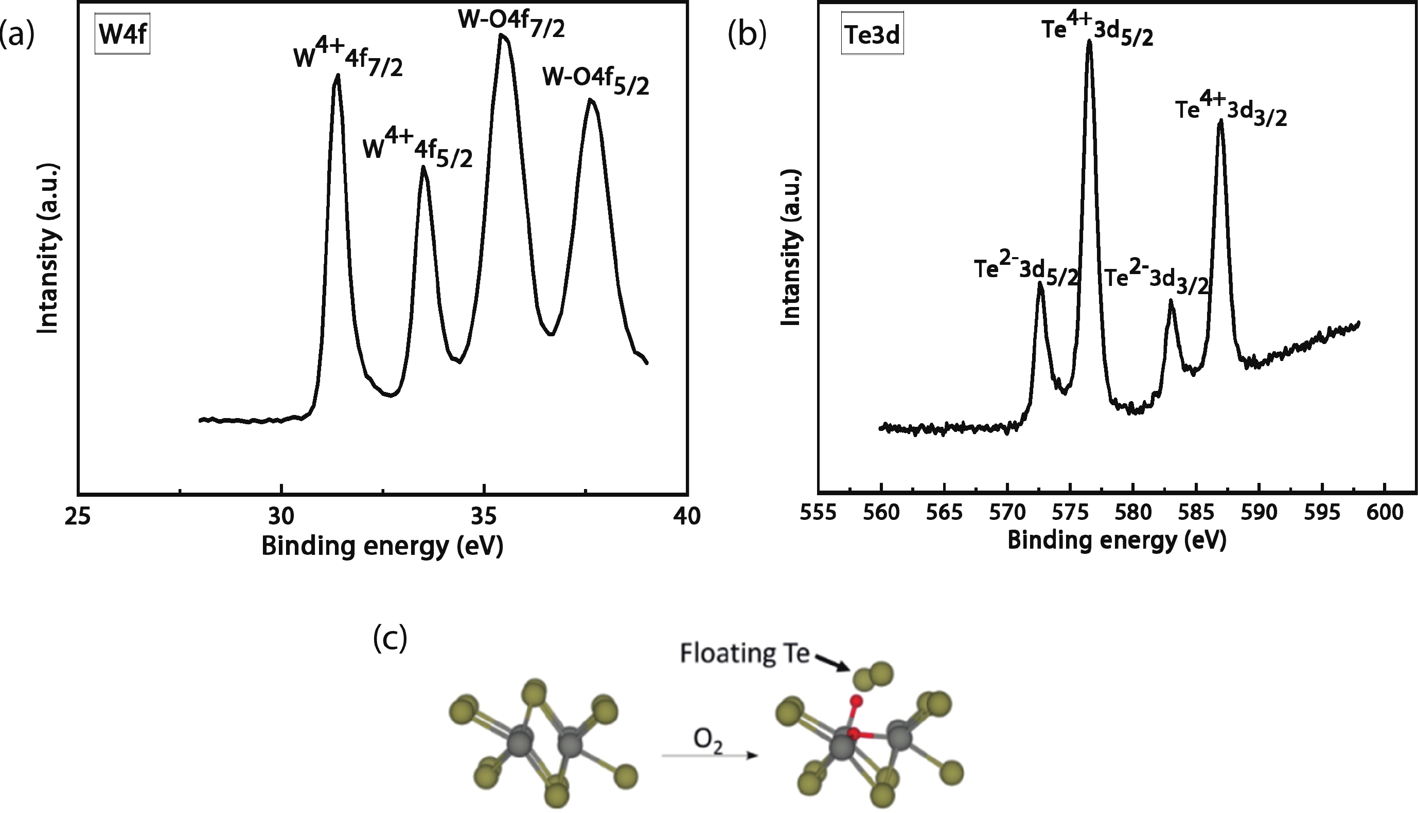
Fig. 5.  (Color online) (a) The XPS curve of the sample at 550°C. (b) The schematic diagram of oxidation principle. (c) The oxidation principle diagram.

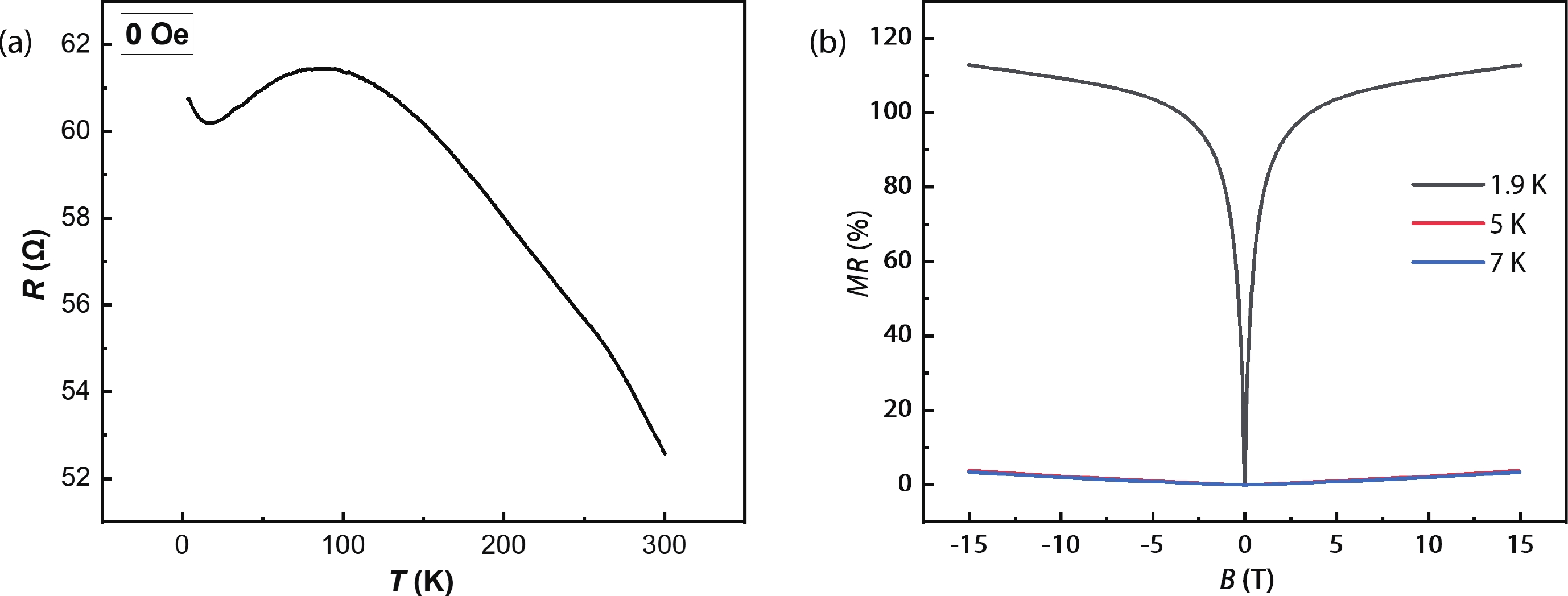
Fig. 6.  (Color online) (a) RT curve and (b) MR curve of tungsten telluride thin films at 550 °C tellurization temperature.

[1]
Qi X L, Zhang S C. Topological insulators and superconductors. Rev Mod Phys, 2011, 83, 1057 doi: 10.1103/RevModPhys.83.1057
[2]
Ghosh B, Gupta A, Bishnoi B. Effects of defects on the electronic properties of WTe2 armchair nanoribbons. J Semicond, 2014, 35, 113002 doi: 10.1088/1674-4926/35/11/113002
[3]
Zhou Z Q, Cui Y, Tan P H, et al. Optical and electrical properties of two-dimensional anisotropic materials. J Semicond, 2019, 40, 061001 doi: 10.1088/1674-4926/40/6/061001
[4]
Zhang P, Zhang Y W, Wei Y, et al. Contact engineering for two-dimensional semiconductors. J Semicond, 2020, 41, 071901 doi: 10.1088/1674-4926/41/7/071901
[5]
Bernevig B A, Hughes T L, Zhang S C. Quantum spin Hall effect and topological phase transition in HgTe quantum wells. Science, 2006, 314, 1757 doi: 10.1126/science.1133734
[6]
König M, Wiedmann S, Brüne C, et al. Quantum spin hall insulator state in HgTe quantum wells. Science, 2007, 318, 766 doi: 10.1126/science.1148047
[7]
Qian X F, Liu J W, Fu L, et al. Quantum spin Hall effect in two-dimensional transition metal dichalcogenides. Science, 2014, 346, 1344 doi: 10.1126/science.1256815
[8]
Liu C C, Feng W X, Yao Y G. Quantum spin Hall effect in silicene and two-dimensional germanium. Phys Rev Lett, 2011, 107, 076802 doi: 10.1103/PhysRevLett.107.076802
[9]
Xu Y, Yan B H, Zhang H J, et al. Large-gap quantum spin hall insulators in tin films. Phys Rev Lett, 2013, 111, 136804 doi: 10.1103/PhysRevLett.111.136804
[10]
Ali M N, Xiong J, Flynn S, et al. Large, non-saturating magnetoresistance in WTe2. Nature, 2014, 514, 205 doi: 10.1038/nature13763
[11]
Luo Y K, Li H, Dai Y M, et al. Hall effect in the extremely large magnetoresistance semimetal WTe2. Appl Phys Lett, 2015, 107, 182411 doi: 10.1063/1.4935240
[12]
Song Y, Zhang Q, Mi W B, et al. Valley polarization and p-/n-type doping of monolayer WTe2 on top of Fe3O4(111). Phys Chem Chem Phys, 2016, 18, 15039 doi: 10.1039/C6CP01986B
[13]
Zhu Z W, Lin X, Liu J, et al. Quantum oscillations, thermoelectric coefficients, and the Fermi surface of semimetallic WTe2. Phys Rev Lett, 2015, 114, 176601 doi: 10.1103/PhysRevLett.114.176601
[14]
Jiang J, Tang F, Pan X C, et al. Signature of strong spin-orbital coupling in the large nonsaturating magnetoresistance material WTe2. Phys Rev Lett, 2015, 115, 166601 doi: 10.1103/PhysRevLett.115.166601
[15]
Fei Z Y, Palomaki T, Wu S F, et al. Edge conduction in monolayer WTe2. Nat Phys, 2017, 13, 677 doi: 10.1038/nphys4091
[16]
Wu S F, Fatemi V, Gibson Q D, et al. Observation of the quantum spin Hall effect up to 100 kelvin in a monolayer crystal. Science, 2018, 359, 76 doi: 10.1126/science.aan6003
[17]
Song Y H, Jia Z Y, Zhang D Q, et al. Observation of Coulomb gap in the quantum spin Hall candidate single-layer 1T’-WTe2. Nat Commun, 2018, 9, 4071 doi: 10.1038/s41467-018-06635-x
[18]
Jia Z Y, Song Y H, Li X B, et al. Direct visualization of a two-dimensional topological insulator in the single-layer 1T'-WTe2. Phys Rev B, 2017, 96, 041108 doi: 10.1103/PhysRevB.96.041108
[19]
Li J, Cheng S, Liu Z X, et al. Centimeter-scale, large-area, few-layer 1T'-WTe2 films by chemical vapor deposition and its long-term stability in ambient condition. J Phys Chem C, 2018, 122, 7005 doi: 10.1021/acs.jpcc.8b00679
[20]
Jiang Y C, Gao J, Wang L. Raman fingerprint for semi-metal WTe2 evolving from bulk to monolayer. Sci Rep, 2016, 6, 19624 doi: 10.1038/srep19624
[21]
Zhou J D, Liu F C, Lin J H, et al. 2D materials: Large-area and high-quality 2D transition metal telluride. Adv Mater, 2017, 29, 1603471 doi: 10.1002/adma.201603471
[22]
Zhou Y, Jang H, Woods J M, et al. Direct synthesis of large-scale WTe2 thin films with low thermal conductivity. Adv Funct Mater, 2017, 27, 1605928 doi: 10.1002/adfm.201605928
[23]
Aslan T, Mtsuko D, Coleman C, et al. Observation of Shubnikov de Haas and aharanov-bohm oscillations in silicon nanowires. arXiv: 1504.02325, 2015
[24]
Wang Y, Wang X, Xu Y, et al. Simultaneous synthesis of WO3– x quantum dots and bundle-like nanowires using a one-pot template-free solvothermal strategy and their versatile applications. Small, 2017, 11, 1310 doi: 10.1002/smll.201603689
[25]
Lu W, Zhang Y D, Zhu Z S, et al. Thin tungsten telluride layer preparation by thermal annealing. Nanotechnology, 2016, 27, 414006 doi: 10.1088/0957-4484/27/41/414006
[26]
Naylor C H, Parkin W M, Gao Z L, et al. Large-area synthesis of high-quality monolayer 1T'-WTe2 flakes. 2D Mater, 2017, 4, 021008 doi: 10.1088/2053-1583/aa5921
[27]
Shi S Y, Li J, Hsu C, et al. Observation of the out-of-plane polarized spin current from CVD grown WTe2. Adv Quantum Tech, 2021, 4, 2100038 doi: 10.1002/qute.202100038
[28]
Chen K, Chen Z, Wan X, et al. A simple method for synthesis of high-quality millimeter-scale 1T' transition-metal telluride and near-field nanooptical properties. Adv Mater, 2017, 29, 1700704 doi: 10.1002/adma.201700704
[29]
Mleczko M J, Xu R L, Okabe K, et al. High Current density and low thermal conductivity of atomically thin semimetallic WTe2. ACS Nano, 2016, 10, 7507 doi: 10.1021/acsnano.6b02368
[30]
Giri A, Yang H, Jang W, et al. Synthesis of atomically thin transition metal ditelluride films by rapid chemical transformation in solution phase. Chem Mater, 2018, 30, 2463 doi: 10.1021/acs.chemmater.8b00684
[31]
Cai P L, Hu J, He L P, et al. Drastic pressure effect on the extremely large magnetoresistance in WTe2: Quantum oscillation study. Phys Rev Lett, 2015, 115, 057202 doi: 10.1103/PhysRevLett.115.057202
[32]
Lv Y Y, Zhang B B, Li X, et al. Dramatically decreased magnetoresistance in non-stoichiometric WTe2 crystals. Sci Rep, 2016, 6, 26903 doi: 10.1038/srep26903
[33]
Pletikosić I, Ali M N, Fedorov A V, et al. Electronic structure basis for the extraordinary magnetoresistance in WTe2. Phys Rev Lett, 2014, 113, 216601 doi: 10.1103/PhysRevLett.113.216601
  • Search

    Advanced Search >>

    GET CITATION

    shu

    Export: BibTex EndNote

    Article Metrics

    Article views: 936 Times PDF downloads: 88 Times Cited by: 0 Times

    History

    Received: 29 May 2022 Revised: 02 June 2022 Online: Accepted Manuscript: 05 August 2022Uncorrected proof: 08 August 2022Published: 01 October 2022

    Catalog

      Email This Article

      User name:
      Email:*请输入正确邮箱
      Code:*验证码错误
      Yumeng Zhang, Zhejia Wang, Jiaheng Feng, Shuaiqiang Ming, Furong Qu, Yang Xia, Meng He, Zhimin Hu, Jing Wang. Synthesis and electromagnetic transport of large-area 2D WTe2 thin film[J]. Journal of Semiconductors, 2022, 43(10): 102002. doi: 10.1088/1674-4926/43/10/102002 ****Yumeng Zhang, Zhejia Wang, Jiaheng Feng, Shuaiqiang Ming, Furong Qu, Yang Xia, Meng He, Zhimin Hu, Jing Wang. 2022: Synthesis and electromagnetic transport of large-area 2D WTe2 thin film. Journal of Semiconductors, 43(10): 102002. doi: 10.1088/1674-4926/43/10/102002
      Citation:
      Yumeng Zhang, Zhejia Wang, Jiaheng Feng, Shuaiqiang Ming, Furong Qu, Yang Xia, Meng He, Zhimin Hu, Jing Wang. Synthesis and electromagnetic transport of large-area 2D WTe2 thin film[J]. Journal of Semiconductors, 2022, 43(10): 102002. doi: 10.1088/1674-4926/43/10/102002 ****
      Yumeng Zhang, Zhejia Wang, Jiaheng Feng, Shuaiqiang Ming, Furong Qu, Yang Xia, Meng He, Zhimin Hu, Jing Wang. 2022: Synthesis and electromagnetic transport of large-area 2D WTe2 thin film. Journal of Semiconductors, 43(10): 102002. doi: 10.1088/1674-4926/43/10/102002

      Synthesis and electromagnetic transport of large-area 2D WTe2 thin film

      doi: 10.1088/1674-4926/43/10/102002
      More Information
      • Yumeng Zhang:received her BS from Nankai University in 2019. She is now a Master’s student at University of Chinese Academy of Science under the supervision of Prof. Yang Xia. Her research focuses on the two-dimensional materials and microelectronic components
      • Furong Qu:is a senior engineer of the Institute of Microelectronics, Chinese Academy of Sciences, graduated from Beijing Institute of Technology in 1997. She currently presides over the major scientific research instrument development projects of the Chinese Academy of Sciences, mainly engaged in the research and development of new principle equipment and material preparation for micro-nano processing, focusing on the preparation, characterization and application of two-dimensional materials and devices
      • Corresponding author: qufurong@ime.ac.cn
      • Received Date: 2022-05-29
      • Revised Date: 2022-06-02
      • Available Online: 2022-08-05

      Catalog

        /

        DownLoad:  Full-Size Img  PowerPoint
        Return
        Return