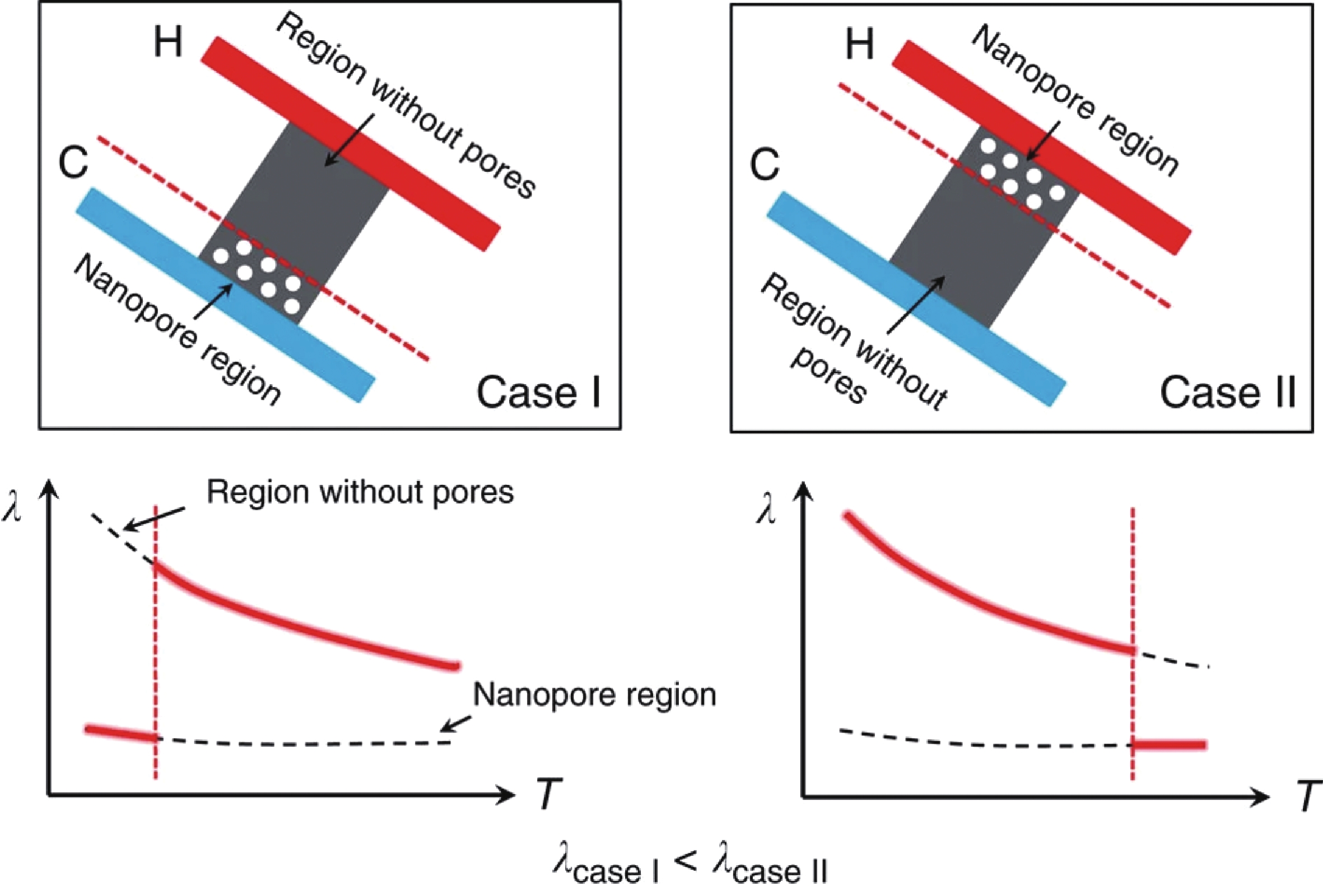
| [1] |
|
| [2] |
Cardoso J M P, Coutinho J G F, Diniz P C. High-performance embedded computing. In: Embedded Computing for High Performance, Amsterdam: Elsevier, 2017, 17
|
| [3] |
|
| [4] |
Malik F K, Talha T, Ahmed F. A parametric study of the effects of critical design parameters on the performance of nanoscale silicon devices. Nanomaterials, 2020, 10, 1987 doi: 10.3390/nano10101987 |
| [5] |
Vasileska D, Raleva K, Goodnick S M. Modeling heating effects in nanoscale devices: The present and the future. J Comput Electron, 2008, 7, 66 doi: 10.1007/s10825-008-0254-y |
| [6] |
|
| [7] |
Sohel Murshed S M, Nieto de Castro C A. A critical review of traditional and emerging techniques and fluids for electronics cooling. Renew Sustain Energy Rev, 2017, 78, 821 doi: 10.1016/j.rser.2017.04.112 |
| [8] |
Roberts N A, Walker D G. A review of thermal rectification observations and models in solid materials. Int J Therm Sci, 2011, 50, 648 doi: 10.1016/j.ijthermalsci.2010.12.004 |
| [9] |
|
| [10] |
Chiu C L, Wu C H, Huang B W, et al. Detecting thermal rectification. AIP Adv, 2016, 6, 121901 doi: 10.1063/1.4968613 |
| [11] |
Chakraborty D, Brooke J, Hulse N C S, et al. Thermal rectification optimization in nanoporous Si using Monte Carlo simulations. J Appl Phys, 2019, 126, 184303 doi: 10.1063/1.5119806 |
| [12] |
Thompson A P, Aktulga H M, Berger R, et al. LAMMPS - a flexible simulation tool for particle-based materials modeling at the atomic, meso, and continuum scales. Comput Phys Commun, 2022, 271, 108171 doi: 10.1016/j.cpc.2021.108171 |
| [13] |
Medrano Sandonas L, Cuba-Supanta G, Gutierrez R, et al. Enhancement of thermal transport properties of asymmetric graphene/hBN nanoribbon heterojunctions by substrate engineering. Carbon, 2017, 124, 642 doi: 10.1016/j.carbon.2017.09.025 |
| [14] |
Wehmeyer G, Yabuki T, Monachon C, et al. Thermal diodes, regulators, and switches: Physical mechanisms and potential applications. Appl Phys Rev, 2017, 4, 041304 doi: 10.1063/1.5001072 |
| [15] |
|
| [16] |
Chen X K, Xie Z X, Zhang Y, et al. Highly efficient thermal rectification in carbon/boron nitride heteronanotubes. Carbon, 2019, 148, 532 doi: 10.1016/j.carbon.2019.03.073 |
| [17] |
Li S, Guo Z X, Ding J W. Interface thermal transport of graphene-based intralayer heterostructures. Phys B, 2019, 561, 164 doi: 10.1016/j.physb.2019.02.064 |
| [18] |
Giazotto F, Bergeret F S. Thermal rectification of electrons in hybrid normal metal-superconductor nanojunctions. Appl Phys Lett, 2013, 103, 242602 doi: 10.1063/1.4846375 |
| [19] |
Wang H D, Hu S Q, Takahashi K, et al. Experimental study of thermal rectification in suspended monolayer graphene. Nat Commun, 2017, 8, 15843 doi: 10.1038/ncomms15843 |
| [20] |
Bahk J H, Bian Z X, Shakouri A. Electron energy filtering by a nonplanar potential to enhance the thermoelectric power factor in bulk materials. Phys Rev B, 2013, 87, 075204 doi: 10.1103/PhysRevB.87.075204 |
| [21] |
Sierra M A, Sánchez D. Strongly nonlinear thermovoltage and heat dissipation in interacting quantum dots. Phys Rev B, 2014, 90, 115313 doi: 10.1103/PhysRevB.90.115313 |
| [22] |
Huberman, Overhauser. Electronic Kapitza conductance at a diamond-Pb interface. Phys Rev B, 1994, 50, 2865 doi: 10.1103/physrevb.50.2865 |
| [23] |
Sergeev A V. Electronic Kapitza conductance due to inelastic electron-boundary scattering. Phys Rev B, 1998, 58, R10199 doi: 10.1103/PhysRevB.58.R10199 |
| [24] |
Majumdar A, Reddy P. Role of electron-phonon coupling in thermal conductance of metal-nonmetal interfaces. Appl Phys Lett, 2004, 84, 4768 doi: 10.1063/1.1758301 |
| [25] |
Walker D. Thermal rectification mechanisms including noncontinuum effects. Proc Jt ASME ISHMT Heat Transf, 2006
|
| [26] |
Mahan G D. Thermionic refrigeration. J Appl Phys, 1994, 76, 4362 doi: 10.1063/1.357324 |
| [27] |
|
| [28] |
Moon J S, Keeler R N. A theoretical consideration of directional effects in heat flow at the interface of dissimilar metals. Int J Heat Mass Transf, 1962, 5, 967 doi: 10.1016/0017-9310(62)90076-5 |
| [29] |
Crossno J, Shi J K, Wang K, et al. Observation of the Dirac fluid and the breakdown of the Wiedemann-Franz law in graphene. Science, 2016, 351, 1058 doi: 10.1126/science.aad0343 |
| [30] |
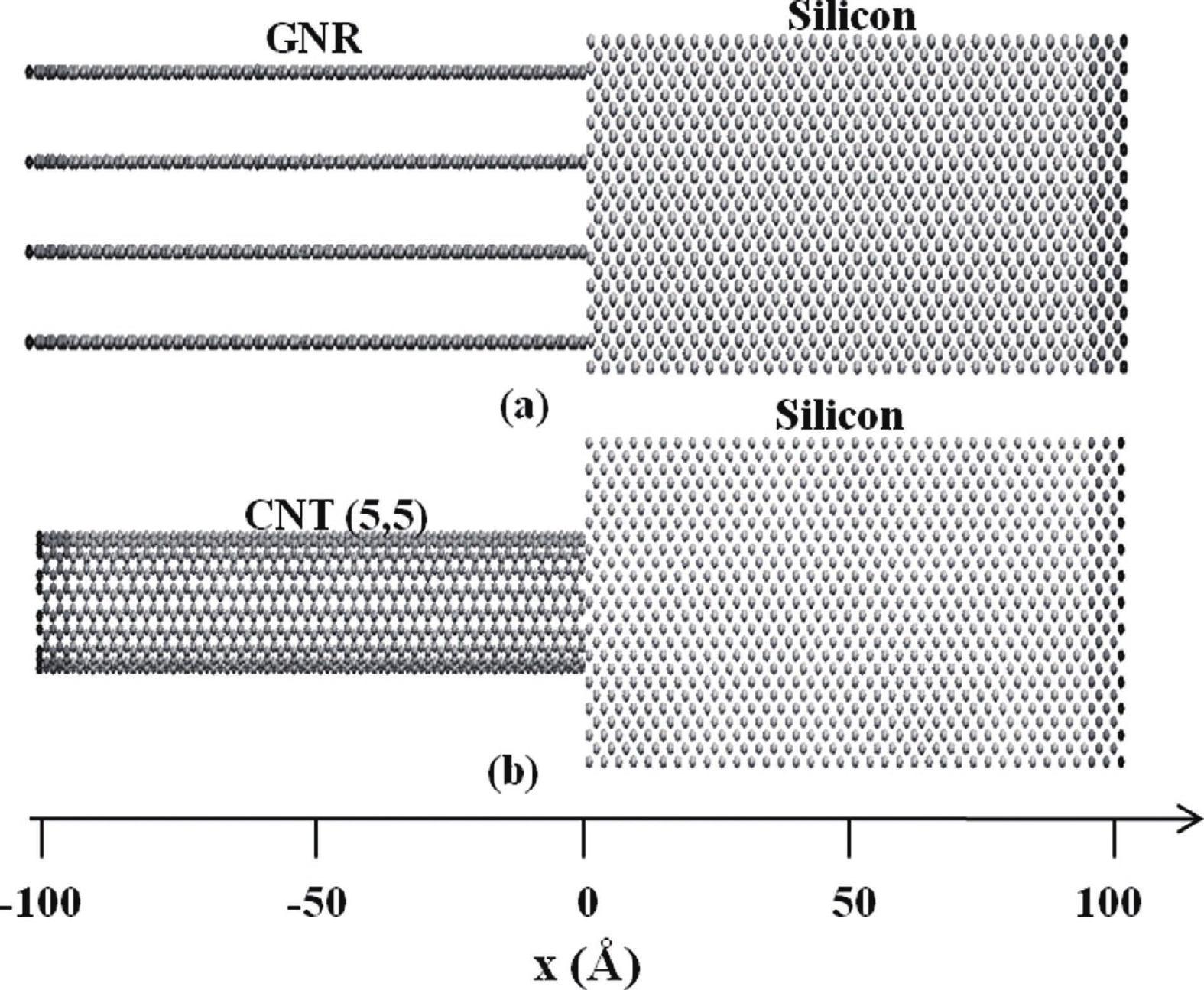
Martínez-Pérez M J, Giazotto F. Efficient phase-tunable Josephson thermal rectifier. Appl Phys Lett, 2013, 102, 182602 doi: 10.1063/1.4804550 |
| [31] |
Martínez-Pérez M J, Fornieri A, Giazotto F. Rectification of electronic heat current by a hybrid thermal diode. Nat Nanotechnol, 2015, 10, 303 doi: 10.1038/nnano.2015.11 |
| [32] |
Breunig D, Zhang S B, Trauzettel B, et al. Directional electron filtering at a superconductor-semiconductor interface. Phys Rev B, 2021, 103, 165414 doi: 10.1103/PhysRevB.103.165414 |
| [33] |
Staring A A M, Molenkamp L W, Alphenaar B W, et al. Coulomb-blockade oscillations in the thermopower of a quantum dot. Europhys Lett, 1993, 22, 57 doi: 10.1209/0295-5075/22/1/011 |
| [34] |
|
| [35] |
Kuo D M T, Chang Y C. Thermoelectric and thermal rectification properties of quantum dot junctions. Phys Rev B, 2010, 81, 205321 doi: 10.1103/PhysRevB.81.205321 |
| [36] |
Zhang Y C, Su S H. Thermal rectification and negative differential thermal conductance based on a parallel-coupled double quantum-dot. Physica A, 2021, 584, 126347 doi: 10.1016/j.physa.2021.126347 |
| [37] |
|
| [38] |
Terraneo M, Peyrard M, Casati G. Controlling the energy flow in nonlinear lattices: A model for a thermal rectifier. Phys Rev Lett, 2002, 88, 094302 doi: 10.1103/PhysRevLett.88.094302 |
| [39] |
Li B W, Lan J H, Wang L. Interface thermal resistance between dissimilar anharmonic lattices. Phys Rev Lett, 2005, 95, 104302 doi: 10.1103/PhysRevLett.95.104302 |
| [40] |
Hu M, Keblinski P, Li B W. Thermal rectification at silicon-amorphous polyethylene interface. Appl Phys Lett, 2008, 92, 211908 doi: 10.1063/1.2937834 |
| [41] |
Kobayashi W, Teraoka Y, Terasaki I. An oxide thermal rectifier. Appl Phys Lett, 2009, 95, 171905 doi: 10.1063/1.3253712 |
| [42] |
Arora A, Hori T, Shiga T, et al. Thermal rectification in restructured graphene with locally modulated temperature dependence of thermal conductivity. Phys Rev B, 2017, 96, 165419 doi: 10.1103/PhysRevB.96.165419 |
| [43] |
Cottrill A L, Strano M S. Analysis of thermal diodes enabled by junctions of phase change materials. Adv Energy Mater, 2015, 5, 1500921 doi: 10.1002/aenm.201500921 |
| [44] |
Dames C. Solid-state thermal rectification with existing bulk materials. J Heat Transf, 2009, 131, 1 doi: 10.1115/1.3089552 |
| [45] |
Ordonez-Miranda J, Hill J M, Joulain K, et al. Conductive thermal diode based on the thermal hysteresis of VO 2 and nitinol. J Appl Phys, 2018, 123, 085102 doi: 10.1063/1.5019854 |
| [46] |
Pallecchi E, Chen Z, Fernandes G E, et al. A thermal diode and novel implementation in a phase-change material. Mater Horiz, 2015, 2, 125 doi: 10.1039/C4MH00193A |
| [47] |
Cottrill A L, Wang S, Liu A T, et al. Dual phase change thermal diodes for enhanced rectification ratios: Theory and experiment. Adv Energy Mater, 2018, 8, 1702692 doi: 10.1002/aenm.201702692 |
| [48] |
Hirata K, Matsunaga T, Singh S, et al. High-performance solid-state thermal diode consisting of Ag 2(S, Se, Te). J Electron Mater, 2020, 49, 2895 doi: 10.1007/s11664-020-07964-8 |
| [49] |
Kasali S O, Ordonez-Miranda J, Joulain K. Conductive thermal diode based on two phase-change materials. Int J Therm Sci, 2020, 153, 106393 doi: 10.1016/j.ijthermalsci.2020.106393 |
| [50] |
Chaves A, Azadani J G, Alsalman H, et al. Bandgap engineering of two-dimensional semiconductor materials. npj 2D Mater Appl, 2020, 4, 29 doi: 10.1038/s41699-020-00162-4 |
| [51] |
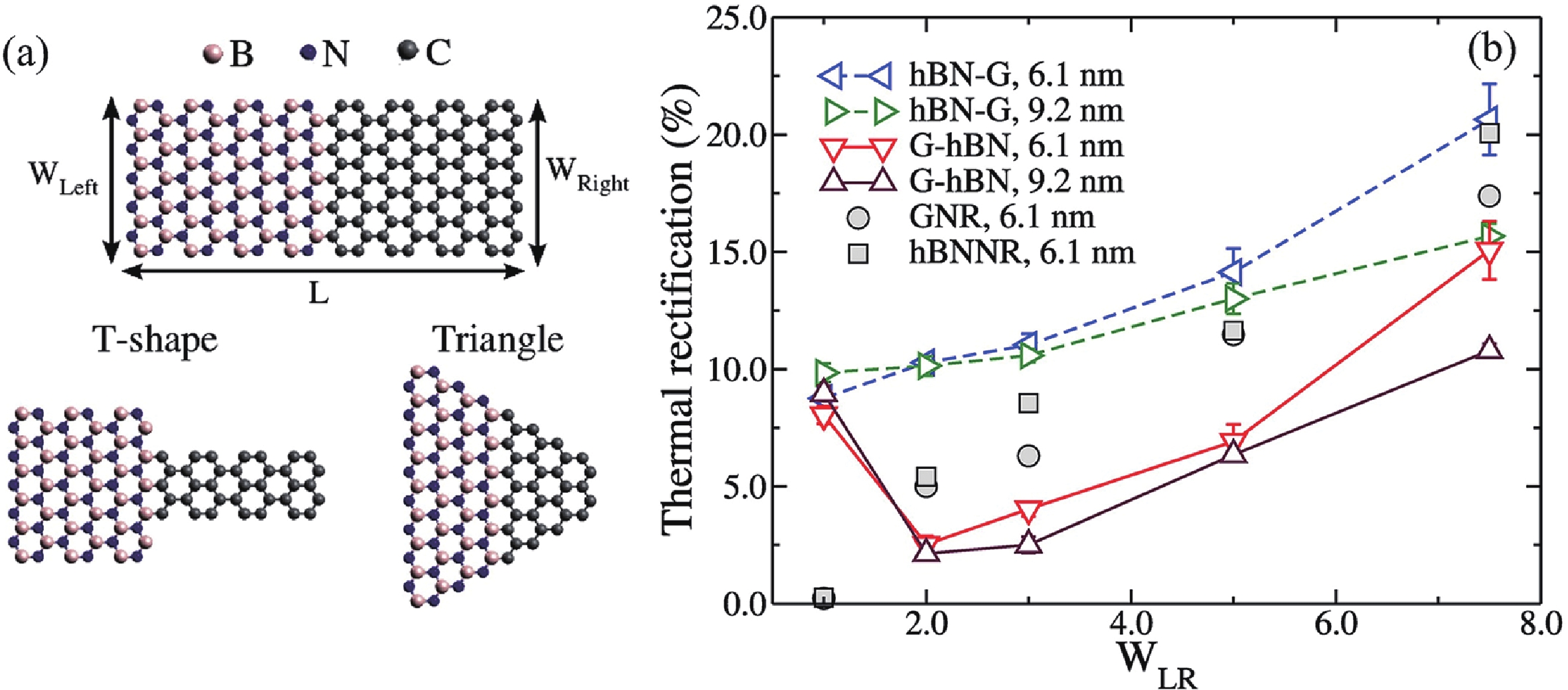
Chen X K, Pang M, Chen T, et al. Thermal rectification in asymmetric graphene/hexagonal boron nitride van der waals heterostructures. ACS Appl Mater Interfaces, 2020, 12, 15517 doi: 10.1021/acsami.9b22498 |
| [52] |
Farzadian O, Razeghiyadaki A, Spitas C, et al. Phonon thermal rectification in hybrid graphene-C 3N: A molecular dynamics simulation. Nanotechnology, 2020, 31, 485401 doi: 10.1088/1361-6528/abb04b |
| [53] |
Wang H, Liu F C, Fu W, et al. Two-dimensional heterostructures: Fabrication, characterization, and application. Nanoscale, 2014, 6, 12250 doi: 10.1039/C4NR03435J |
| [54] |
Liu B, Baimova J A, Reddy C D, et al. Interface thermal conductance and rectification in hybrid graphene/silicene monolayer. Carbon, 2014, 79, 236 doi: 10.1016/j.carbon.2014.07.064 |
| [55] |
Rajabpour A, Bazrafshan S, Volz S. Carbon-nitride 2D nanostructures: Thermal conductivity and interfacial thermal conductance with the silica substrate. Phys Chem Chem Phys, 2019, 21, 2507 doi: 10.1039/C8CP06992A |
| [56] |
Zhong W R, Huang W H, Deng X R, et al. Thermal rectification in thickness-asymmetric graphene nanoribbons. Appl Phys Lett, 2011, 99, 193104 doi: 10.1063/1.3659474 |
| [57] |
Yousefi F, Khoeini F, Rajabpour A. Thermal rectification and interfacial thermal resistance in hybrid pillared-graphene and graphene: A molecular dynamics and continuum approach. Nanotechnology, 2020, 31, 285707 doi: 10.1088/1361-6528/ab8420 |
| [58] |
Cao H Y, Xiang H J, Gong X G. Unexpected large thermal rectification in asymmetric grain boundary of graphene. Solid State Commun, 2012, 152, 1807 doi: 10.1016/j.ssc.2012.07.013 |
| [59] |
Yamada M, Yamakita Y, Ohno K. Phonon dispersions of hydrogenated and dehydrogenated carbon nanoribbons. Phys Rev B, 2008, 77, 054302 doi: 10.1103/PhysRevB.77.054302 |
| [60] |
Yamamoto T, Watanabe K, Mii K. Empirical-potential study of phonon transport in graphitic ribbons. Phys Rev B, 2004, 70, 245402 doi: 10.1103/PhysRevB.70.245402 |
| [61] |
Vallabhaneni A K, Qiu B, Hu J N, et al. Interfacial thermal conductance limit and thermal rectification across vertical carbon nanotube/graphene nanoribbon-silicon interfaces. J Appl Phys, 2013, 113, 064311 doi: 10.1063/1.4790367 |
| [62] |
Li T, Tang Z N, Huang Z X, et al. Interfacial thermal resistance of 2D and 1D carbon/hexagonal boron nitride van der Waals heterostructures. Carbon, 2016, 105, 566 doi: 10.1016/j.carbon.2016.05.001 |
| [63] |
Lee S H, Choi M S, Lee J, et al. High performance vertical tunneling diodes using graphene/hexagonal boron nitride/graphene hetero-structure. Appl Phys Lett, 2014, 104, 053103 doi: 10.1063/1.4863840 |
| [64] |
Chen C C, Li Z, Shi L, et al. Thermoelectric transport across graphene/hexagonal boron nitride/graphene heterostructures. Nano Res, 2015, 8, 666 doi: 10.1007/s12274-014-0550-8 |
| [65] |
Kim E, Yu T H, Song E S, et al. Chemical vapor deposition-assembled graphene field-effect transistor on hexagonal boron nitride. Appl Phys Lett, 2011, 98, 262103 doi: 10.1063/1.3604012 |
| [66] |
Bui K, Nguyen H, Cousin C, et al. Thermal behavior of double-walled carbon nanotubes and evidence of thermal rectification. J Phys Chem C, 2012, 116, 4449 doi: 10.1021/jp2107878 |
| [67] |
Chang C W, Okawa D, Majumdar A, et al. Solid-state thermal rectifier. Science, 2006, 314, 1121 doi: 10.1126/science.1132898 |
| [68] |
Desmarchelier P, Tanguy A, Termentzidis K. Thermal rectification in asymmetric two-phase nanowires. Phys Rev B, 2021, 103, 014202 doi: 10.1103/PhysRevB.103.014202 |
| [69] |
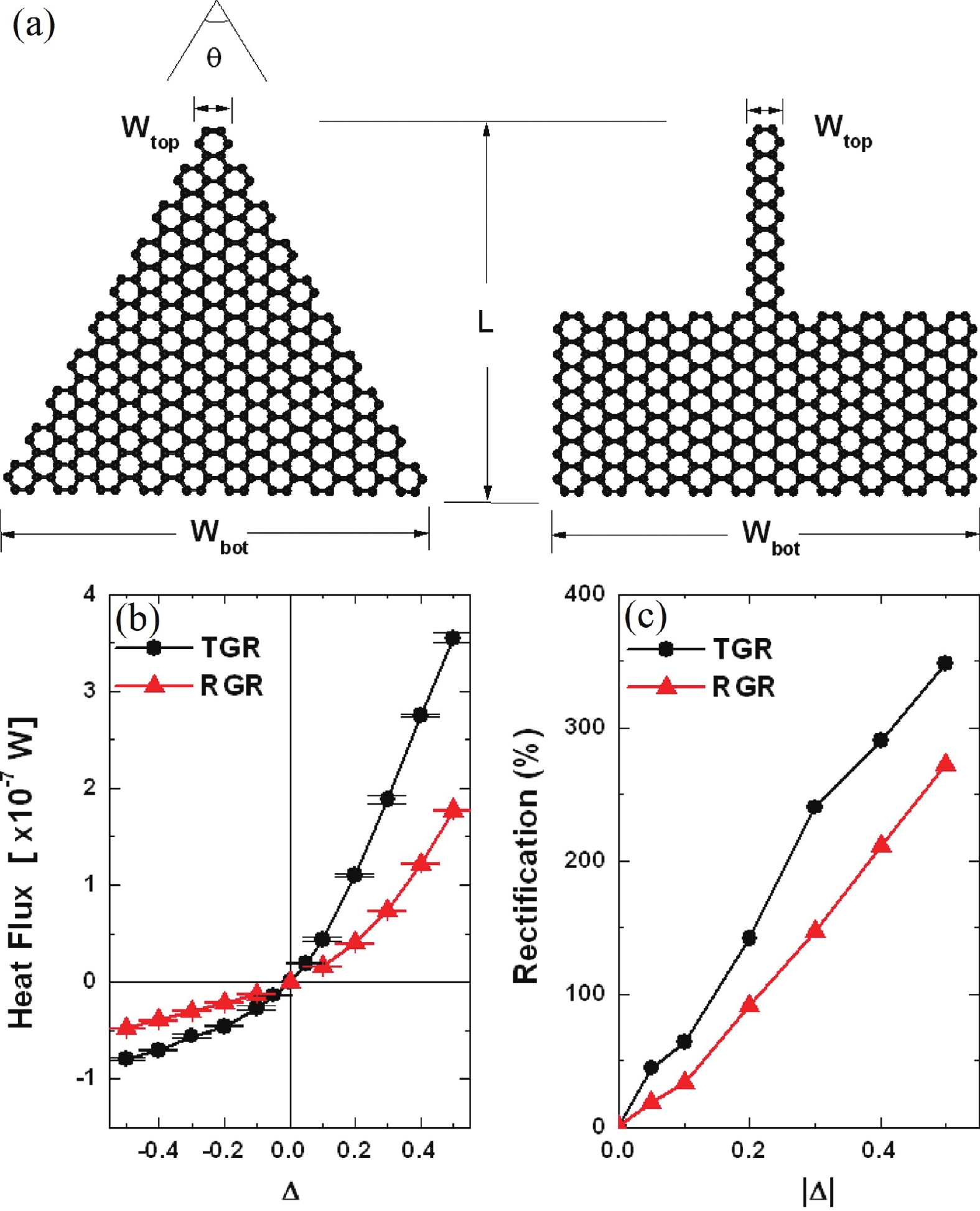
Yang N, Zhang G, Li B W. Thermal rectification in asymmetric graphene ribbons. Appl Phys Lett, 2009, 95, 033107 doi: 10.1063/1.3183587 |
| [70] |
Hu J N, Ruan X L, Chen Y P. Thermal conductivity and thermal rectification in graphene nanoribbons: A molecular dynamics study. Nano Lett, 2009, 9, 2730 doi: 10.1021/nl901231s |
| [71] |
Wang Y, Vallabhaneni A, Hu J N, et al. Phonon lateral confinement enables thermal rectification in asymmetric single-material nanostructures. Nano Lett, 2014, 14, 592 doi: 10.1021/nl403773f |
| [72] |
Medrano Sandonas L, Gutierrez R, Dianat A, et al. Engineering thermal rectification in MoS 2 nanoribbons: A non-equilibrium molecular dynamics study. RSC Adv, 2015, 5, 54345 doi: 10.1039/C5RA05733G |
| [73] |
Yang X, Zheng X H, Liu Q S, et al. Experimental study on thermal conductivity and rectification in suspended monolayer MoS 2. ACS Appl Mater Interfaces, 2020, 12, 28306 doi: 10.1021/acsami.0c07544 |
| [74] |
|
| [75] |
Miller J, Jang W, Dames C. Thermal rectification by ballistic phonons in asymmetric nanostructures. Proceedings of ASME 2009 Heat Transfer Summer Conference, 2010, 317
|
| [76] |
Hayashi H, Ito Y, Takahashi K. Thermal rectification of asymmetrically-defective materials. J Mech Sci Technol, 2011, 25, 27 doi: 10.1007/s12206-010-1008-x |
| [77] |
|
| [78] |
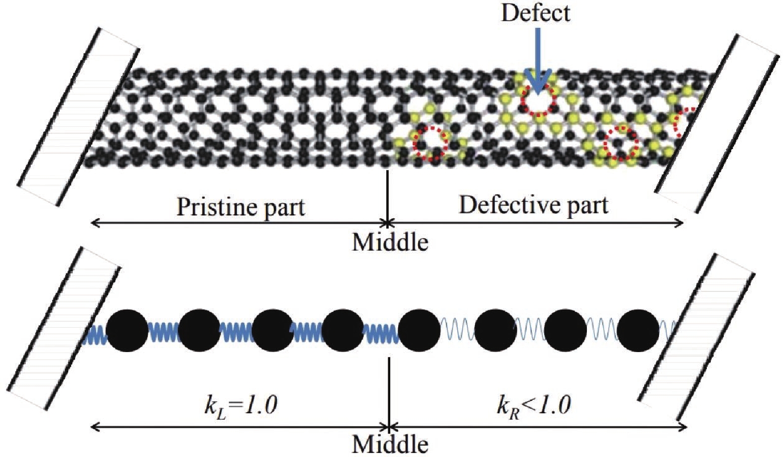
Yousefzadi Nobakht A, Ashraf Gandomi Y, Wang J Q, et al. Thermal rectification via asymmetric structural defects in graphene. Carbon, 2018, 132, 565 doi: 10.1016/j.carbon.2018.02.087 |
| [79] |
Hu S Q, Chen J, Yang N, et al. Thermal transport in graphene with defect and doping: Phonon modes analysis. Carbon, 2017, 116, 139 doi: 10.1016/j.carbon.2017.01.089 |
| [80] |
Yousefi F, Khoeini F, Rajabpour A. Thermal conductivity and thermal rectification of nanoporous graphene: A molecular dynamics simulation. Int J Heat Mass Transf, 2020, 146, 118884 doi: 10.1016/j.ijheatmasstransfer.2019.118884 |
| [81] |
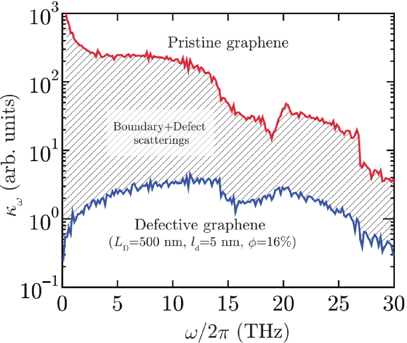
Zhao W W, Wang Y L, Wu Z T, et al. Defect-engineered heat transport in graphene: A route to high efficient thermal rectification. Sci Rep, 2015, 5, 11962 doi: 10.1038/srep11962 |
| [82] |
Kasprzak M, Sledzinska M, Zaleski K, et al. High-temperature silicon thermal diode and switch. Nano Energy, 2020, 78, 105261 doi: 10.1016/j.nanoen.2020.105261 |


 DownLoad: