


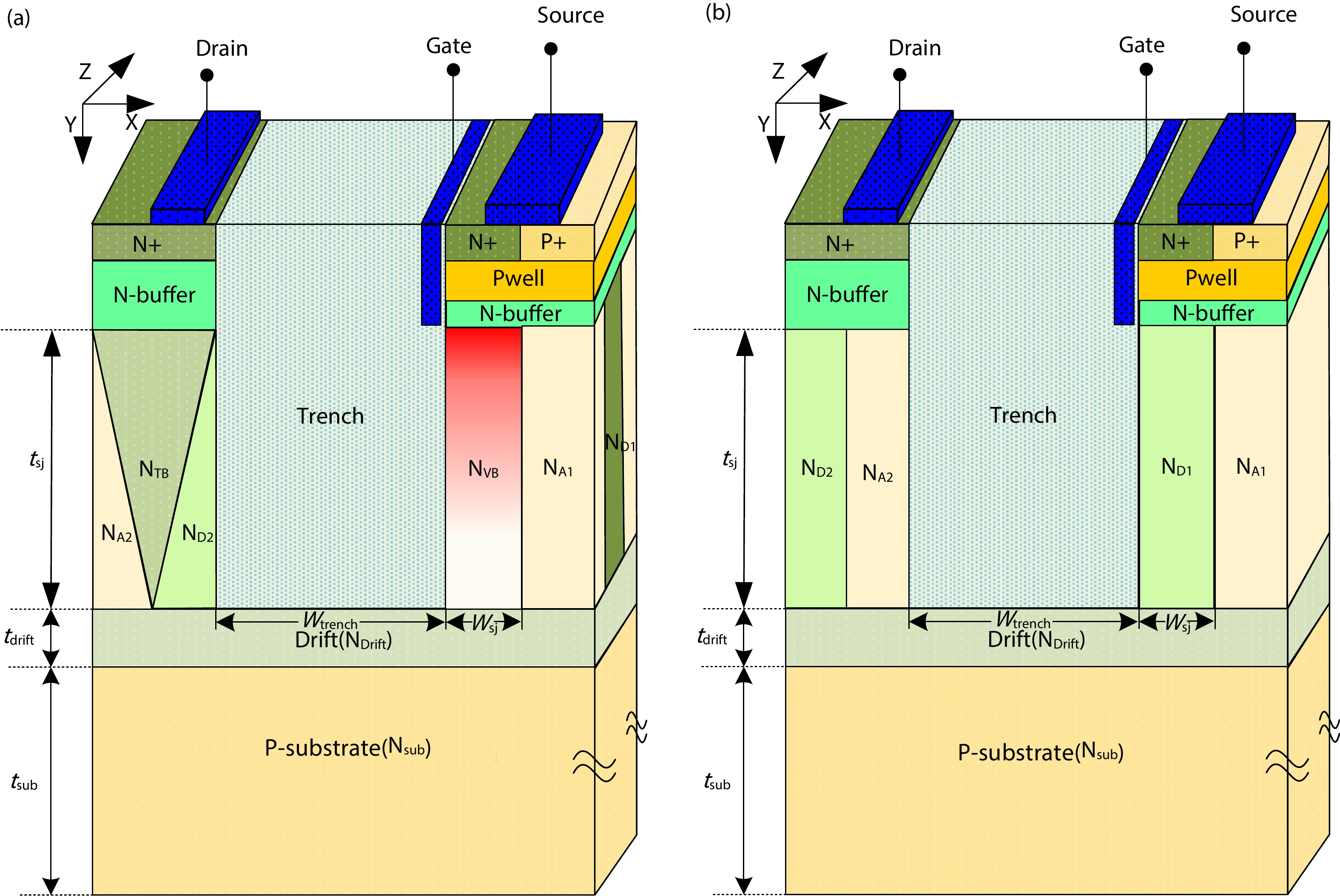
Fig. 1.
(Color online) The structure of (a) DC DT SJ LDMOS and (b) Con. DT SJ LDMOS.
ARTICLES
Lijuan Wu, Shaolian Su, Xing Chen, Jinsheng Zeng and Haifeng Wu
Corresponding author: Lijuan Wu, 305719669@qq.com
Abstract: A deep trench super-junction LDMOS with double charge compensation layer (DC DT SJ LDMOS) is proposed in this paper. Due to the capacitance effect of the deep trench which is known as silicon–insulator–silicon (SIS) capacitance, the charge balance in the super-junction region of the conventional deep trench SJ LDMOS (Con. DT SJ LDMOS) device will be broken, resulting in breakdown voltage (BV) of the device drops. DC DT SJ LDMOS solves the SIS capacitance effect by adding a vertical variable doped charge compensation layer and a triangular charge compensation layer inside the Con. DT SJ LDMOS device. Therefore, the drift region reaches an ideal charge balance state again. The electric field is optimized by double charge compensation and gate field plate so that the breakdown voltage of the proposed device is improved sharply, meanwhile the enlarged on-current region reduces its specific on-resistance. The simulation results show that compared with the Con. DT SJ LDMOS, the BV of the DC DT SJ LDMOS has been increased from 549.5 to 705.5 V, and the Ron,sp decreased to 23.7 mΩ·cm2.
Keywords: double charge compensation layer, super-junction, deep trench, SIS capacitance
| [1] |
Coe D J. High voltage semiconductor device. United States Patent US 4754310, 1988
|
| [2] |
Chen X. Semiconductor power devices with alternating conductivity type high-voltage breakdown regions. United States Patent US 5216275, 1993
|
| [3] |
Zitouni M, Morancho F, Rossel P, et al. A new concept for the lateral DMOS transistor for smart power IC's. 11th International Symposium on Power Semiconductor Devices and ICs, 1999, 73 doi: 10.1109/ISPSD.1999.764055
|
| [4] |
Williams R K, Darwish M N, Blanchard R A, et al. The trench power MOSFET: Part I—History, technology, and prospects. IEEE Trans Electron Devices, 2017, 64, 674 doi: 10.1109/TED.2017.2653239
|
| [5] |
Theolier L, Mahfoz-Kotb H, Isoird K, et al. A new junction termination using a deep trench filled with BenzoCycloButene. IEEE Electron Device Lett, 2009, 30, 687 doi: 10.1109/LED.2009.2020348
|
| [6] |
Xia C, Cheng X H, Wang Z J, et al. Improvement of SOI trench LDMOS performance with double vertical metal field plate. IEEE Trans Electron Devices, 2014, 61, 3477 doi: 10.1109/TED.2014.2349553
|
| [7] |
Park J, Ko K, Eum J, et al. A proposal of LDMOS using Deep Trench poly field plate. 2015 IEEE 27th International Symposium on Power Semiconductor Devices & IC's, 2015, 149 doi: 10.1109/ISPSD.2015.7123411
|
| [8] |
Cao Z, Duan B X, Shi T T, et al. Theory analyses of SJ-LDMOS with multiple floating buried layers based on bulk electric field modulation. IEEE Trans Electron Devices, 2018, 65, 2565 doi: 10.1109/TED.2018.2827064
|
| [9] |
Cheng J J, Li P, Chen W Z, et al. Simulation study of a super-junction deep-trench LDMOS with a trapezoidal trench. IEEE J Electron Devices Soc, 2018, 6, 1091 doi: 10.1109/JEDS.2018.2867344
|
| [10] |
Zhou K, Luo X R, Li Z J, et al. Analytical model and new structure of the variable-k dielectric trench LDMOS with improved breakdown voltage and specific ON-resistance. IEEE Trans Electron Devices, 2015, 62, 3334 doi: 10.1109/TED.2015.2466694
|
| [11] |
Yang D, Hu S D, Lei J M, et al. An ultra-low specific on-resistance double-gate trench SOI LDMOS with P/N Pillars. Superlattices Microstruct, 2017, 112, 269 doi: 10.1016/j.spmi.2017.09.033
|
| [12] |
Cheng J J, Chen W Z, Li P. Improvement of deep-trench LDMOS with variation vertical doping for charge-balance super-junction. IEEE Trans Electron Devices, 2018, 65, 1404 doi: 10.1109/TED.2018.2802485
|
| [13] |
Iqbal M M H, Udrea F, Napoli E. On the static performance of the RESURF LDMOSFETS for power ICs. 2009 21st International Symposium on Power Semiconductor Devices & IC's, 2009, 247 doi: 10.1109/ISPSD.2009.5158048
|
| [14] |
Duan B X, Yuan S, Cao Z, et al. New superjunction LDMOS with the complete charge compensation by the electric field modulation. IEEE Electron Device Lett, 2014, 35, 1115 doi: 10.1109/LED.2014.2359293
|
| [15] |
Wang Y D, Duan B X, Zhang C, et al. AC-SJ VDMOS with ultra-low resistance. Micro Nano Lett, 2020, 15, 230 doi: 10.1049/mnl.2019.0497
|
| [16] |
Zhang W T, Wang R, Cheng S K, et al. Optimization and experiments of lateral semi-superjunction device based on normalized current-carrying capability. IEEE Electron Device Lett, 2019, 40, 1969 doi: 10.1109/LED.2019.2948198
|
| [17] |
Iwamoto S, Takahashi K, Kuribayashi H, et al. Above 500V class Superjunction MOSFETs fabricated by deep trench etching and epitaxial growth. The 17th International Symposium on Power Semiconductor Devices and ICs, 2005, 31 doi: 10.1109/ISPSD.2005.1487943
|
| [18] |
Nautiyal P, Agrawal A, Kumari S, et al. Electrical characteristic investigation of variation vertical doping superjunction UMOS. 2019 IEEE 16th India Council International Conference, 2019, 1 doi: 10.1109/INDICON47234.2019.9030340
|
| [19] |
Kushwaha P K, Nautiyal P, Gupta A, et al. An improved SJ UMOS with modified gate electrode to reduce gate charge. 2019 9th Annual Information Technology, Electromechanical Engineering and Microelectronics Conference, 2019, 81 doi: 10.1109/IEMECONX.2019.8877004
|
| [20] |
Wu L J, Ding Q L, Chen J Q. Improved deep trench super-junction LDMOS breakdown voltage by shielded silicon-insulator-silicon capacitor. Silicon, 2021, 13, 3441 doi: 10.1007/s12633-020-00771-0
|
| [21] |
Chen W Z, He L J, Han Z S, et al. The simulation study of the SOI trench LDMOS with lateral super junction. IEEE J Electron Devices Soc, 2018, 6, 708 doi: 10.1109/JEDS.2018.2842236
|
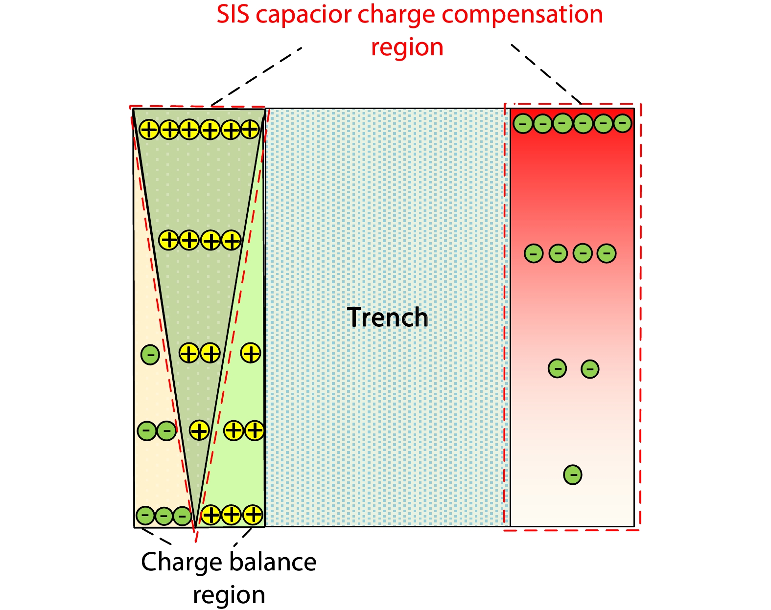
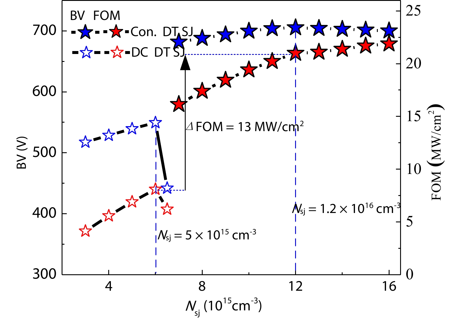
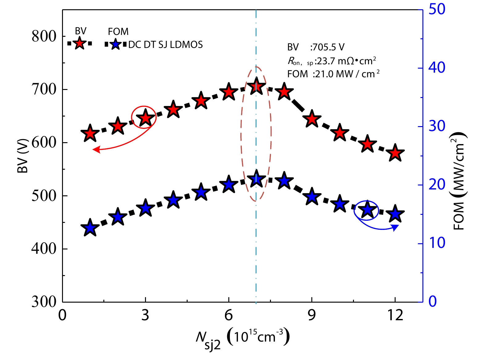
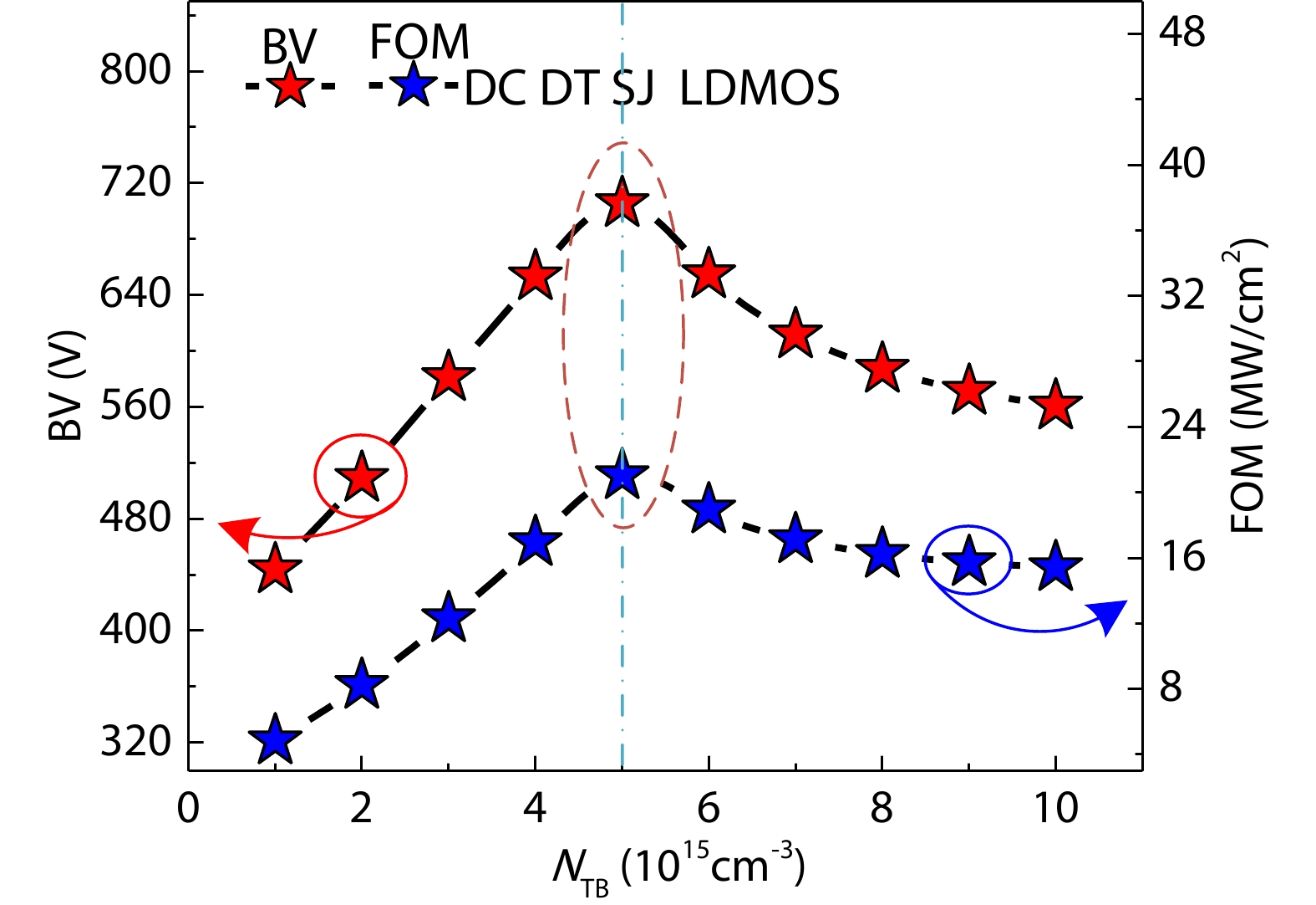
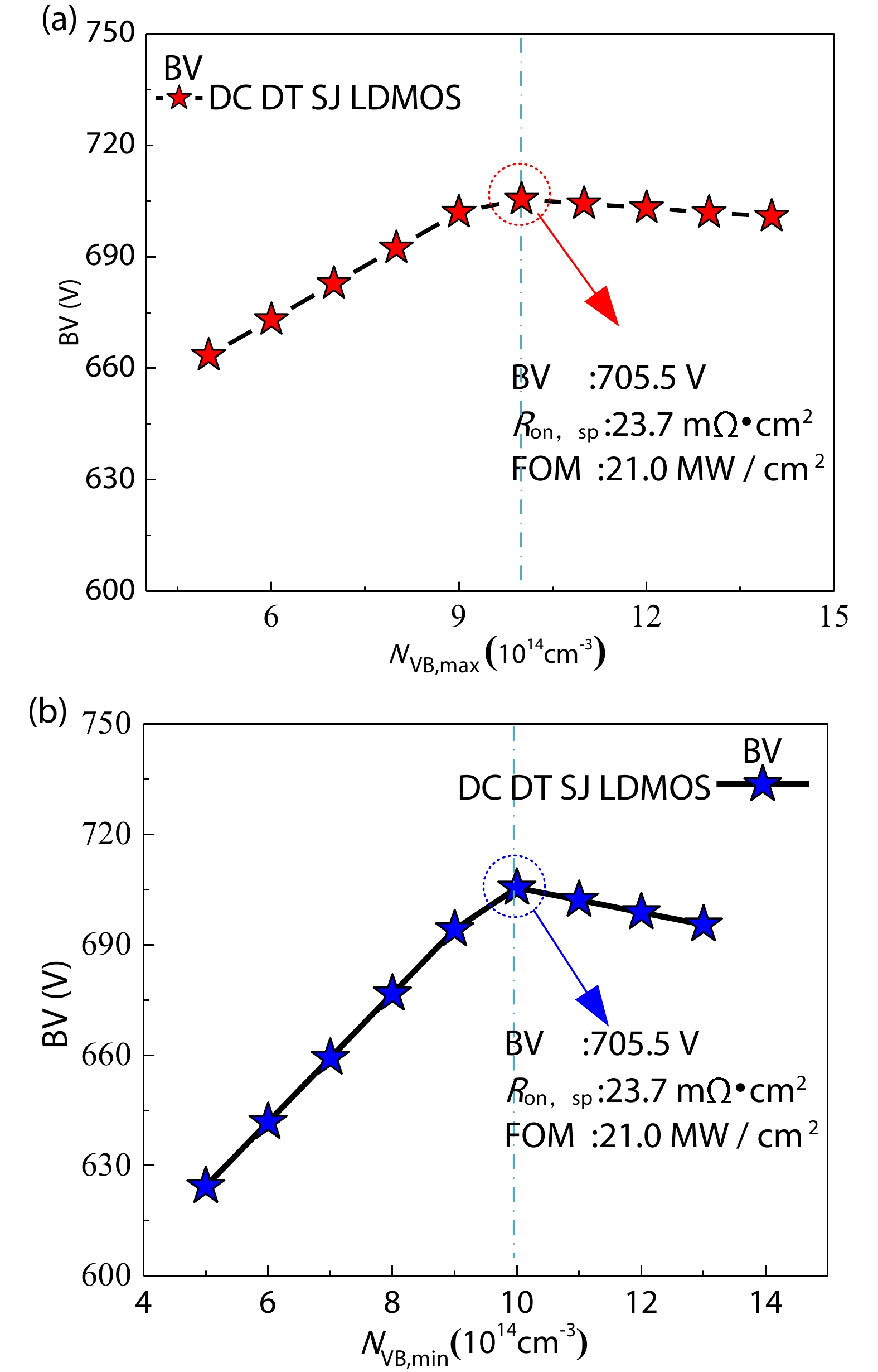
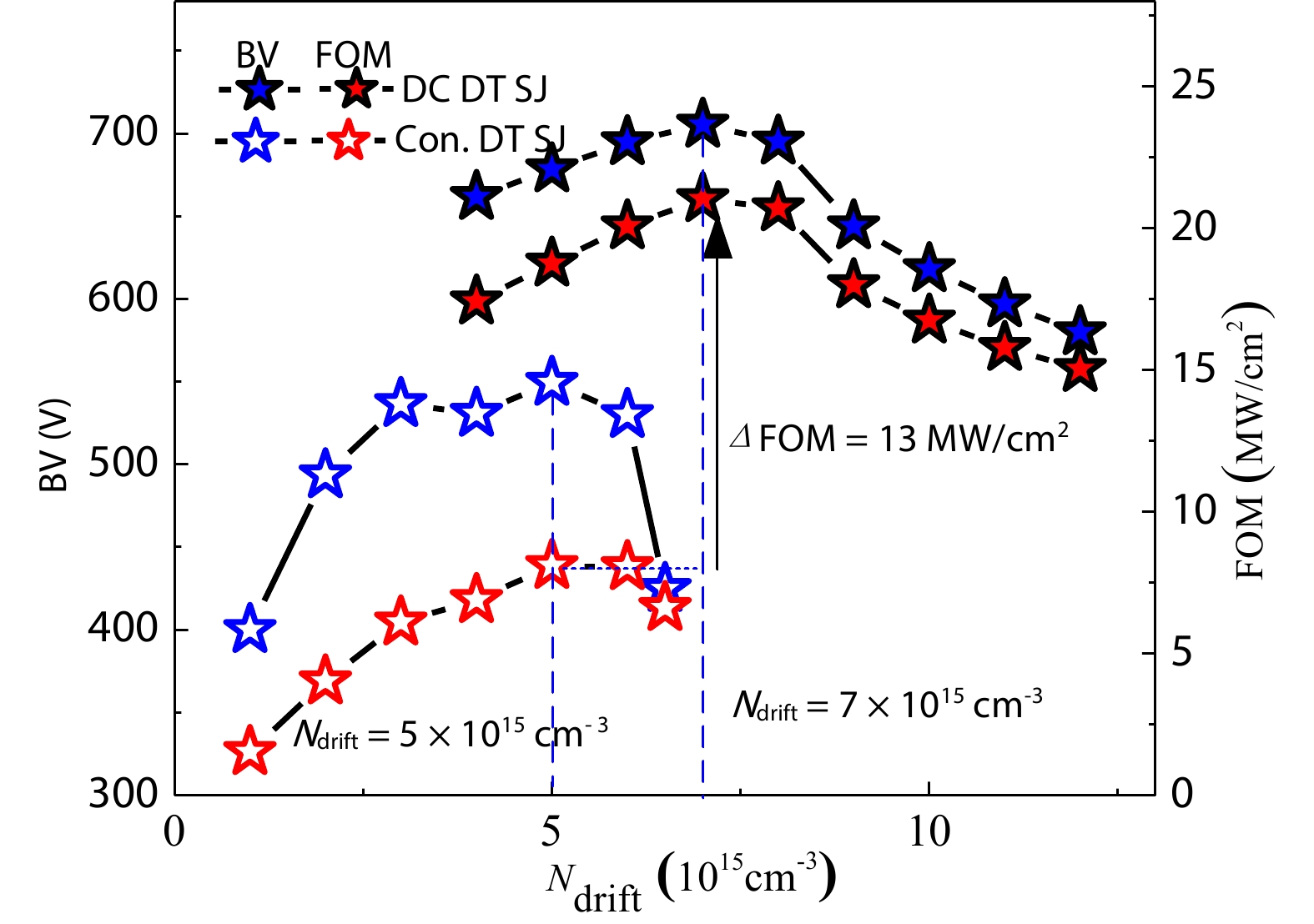
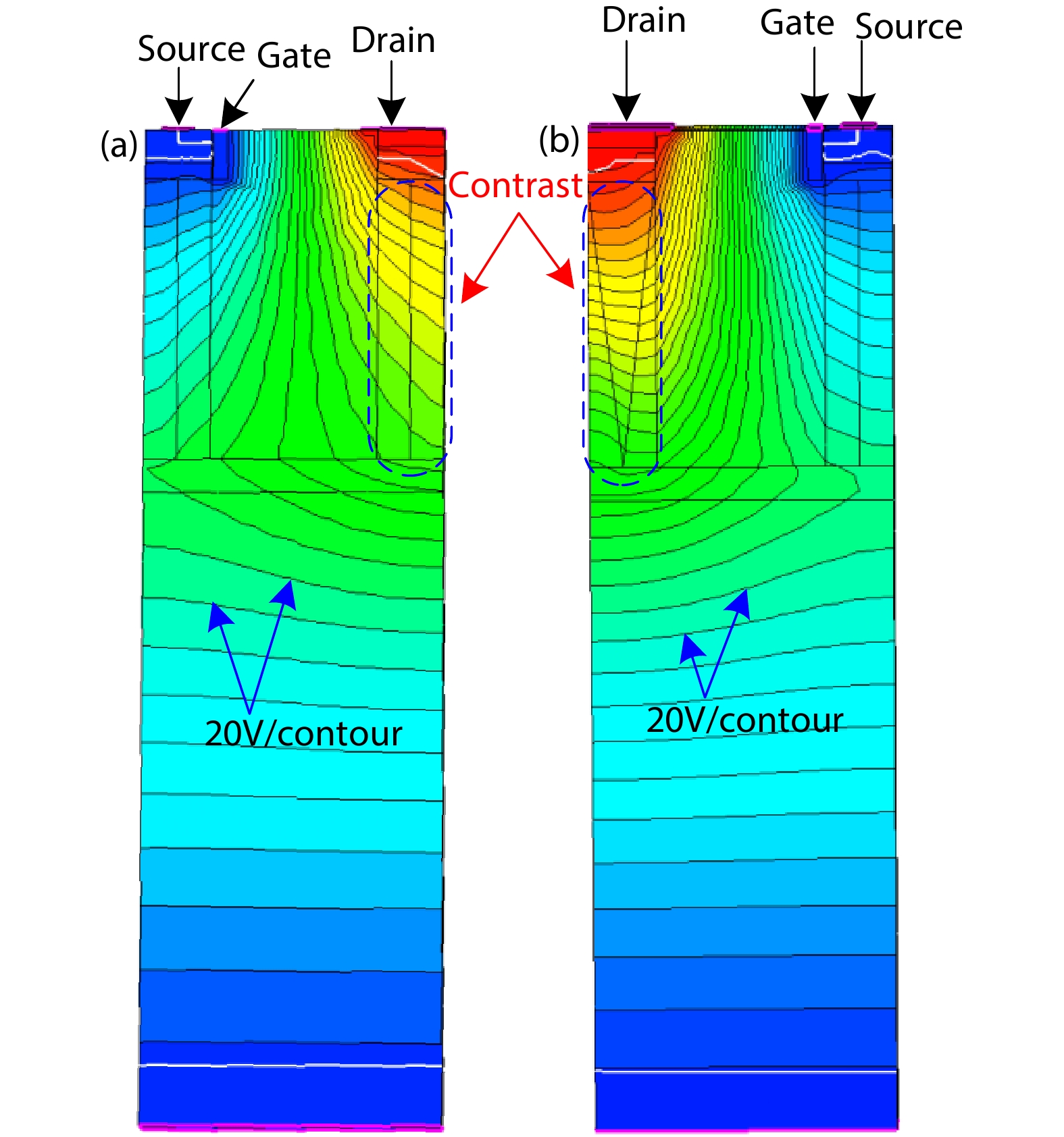
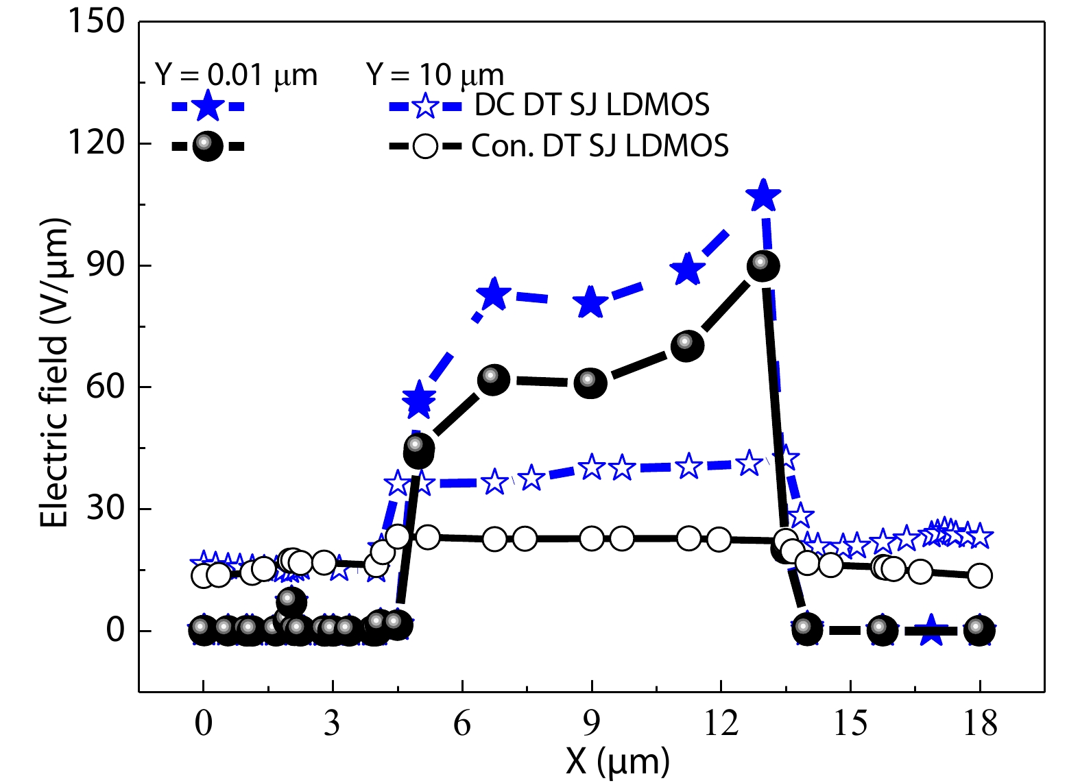

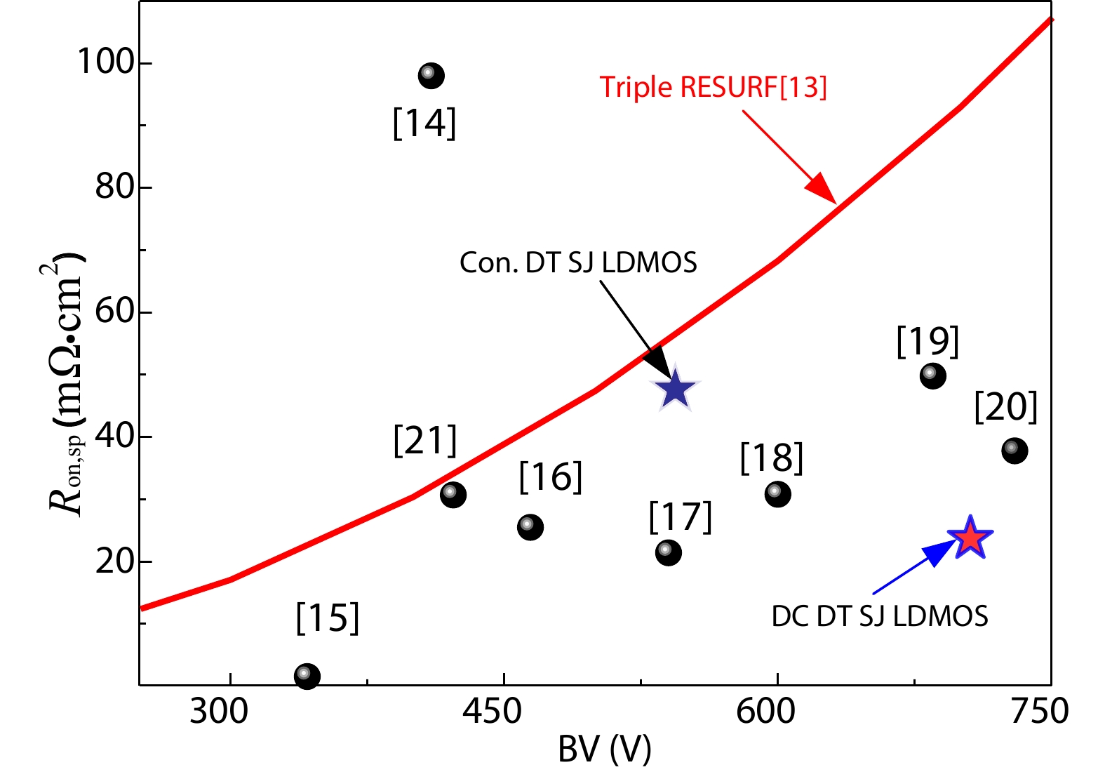
Table 1. Key parameters used in simulation.
| Parameter | Symbol | DC DT SJ LDMOS | Con. DT SJ LDMOS | Unit |
| Width of SiO2 trench | Wtrench | 10 | 10 | μm |
| Width of PN pillar | Wsj | 2 | 2 | μm |
| Thickness of PN pillar | tsj | 17 | 17 | μm |
| Thickness of drift region | tdrift | 2 | 2 | μm |
| Thickness of substrate | tsub | 38 | 38 | μm |
| Doping concentration of N/P pillar at source | ND1/NA1(Nsj) | Optimized | Optimized | cm–3 |
| Doping concentration of triangular-like SJ N/P pillar at drain | ND2/NA2(Nsj2) | Optimized | Optimized | cm–3 |
| Doping concentration of inverted triangular charge compensation layer | NTB | Optimized | – | cm–3 |
| Vertical variable doping concentration | NVB | Optimized | – | cm–3 |
| Doping concentration of N drift region | Ndrift | Optimized | Optimized | cm–3 |
 DownLoad: CSV
| [1] |
Coe D J. High voltage semiconductor device. United States Patent US 4754310, 1988
|
| [2] |
Chen X. Semiconductor power devices with alternating conductivity type high-voltage breakdown regions. United States Patent US 5216275, 1993
|
| [3] |
Zitouni M, Morancho F, Rossel P, et al. A new concept for the lateral DMOS transistor for smart power IC's. 11th International Symposium on Power Semiconductor Devices and ICs, 1999, 73 doi: 10.1109/ISPSD.1999.764055
|
| [4] |
Williams R K, Darwish M N, Blanchard R A, et al. The trench power MOSFET: Part I—History, technology, and prospects. IEEE Trans Electron Devices, 2017, 64, 674 doi: 10.1109/TED.2017.2653239
|
| [5] |
Theolier L, Mahfoz-Kotb H, Isoird K, et al. A new junction termination using a deep trench filled with BenzoCycloButene. IEEE Electron Device Lett, 2009, 30, 687 doi: 10.1109/LED.2009.2020348
|
| [6] |
Xia C, Cheng X H, Wang Z J, et al. Improvement of SOI trench LDMOS performance with double vertical metal field plate. IEEE Trans Electron Devices, 2014, 61, 3477 doi: 10.1109/TED.2014.2349553
|
| [7] |
Park J, Ko K, Eum J, et al. A proposal of LDMOS using Deep Trench poly field plate. 2015 IEEE 27th International Symposium on Power Semiconductor Devices & IC's, 2015, 149 doi: 10.1109/ISPSD.2015.7123411
|
| [8] |
Cao Z, Duan B X, Shi T T, et al. Theory analyses of SJ-LDMOS with multiple floating buried layers based on bulk electric field modulation. IEEE Trans Electron Devices, 2018, 65, 2565 doi: 10.1109/TED.2018.2827064
|
| [9] |
Cheng J J, Li P, Chen W Z, et al. Simulation study of a super-junction deep-trench LDMOS with a trapezoidal trench. IEEE J Electron Devices Soc, 2018, 6, 1091 doi: 10.1109/JEDS.2018.2867344
|
| [10] |
Zhou K, Luo X R, Li Z J, et al. Analytical model and new structure of the variable-k dielectric trench LDMOS with improved breakdown voltage and specific ON-resistance. IEEE Trans Electron Devices, 2015, 62, 3334 doi: 10.1109/TED.2015.2466694
|
| [11] |
Yang D, Hu S D, Lei J M, et al. An ultra-low specific on-resistance double-gate trench SOI LDMOS with P/N Pillars. Superlattices Microstruct, 2017, 112, 269 doi: 10.1016/j.spmi.2017.09.033
|
| [12] |
Cheng J J, Chen W Z, Li P. Improvement of deep-trench LDMOS with variation vertical doping for charge-balance super-junction. IEEE Trans Electron Devices, 2018, 65, 1404 doi: 10.1109/TED.2018.2802485
|
| [13] |
Iqbal M M H, Udrea F, Napoli E. On the static performance of the RESURF LDMOSFETS for power ICs. 2009 21st International Symposium on Power Semiconductor Devices & IC's, 2009, 247 doi: 10.1109/ISPSD.2009.5158048
|
| [14] |
Duan B X, Yuan S, Cao Z, et al. New superjunction LDMOS with the complete charge compensation by the electric field modulation. IEEE Electron Device Lett, 2014, 35, 1115 doi: 10.1109/LED.2014.2359293
|
| [15] |
Wang Y D, Duan B X, Zhang C, et al. AC-SJ VDMOS with ultra-low resistance. Micro Nano Lett, 2020, 15, 230 doi: 10.1049/mnl.2019.0497
|
| [16] |
Zhang W T, Wang R, Cheng S K, et al. Optimization and experiments of lateral semi-superjunction device based on normalized current-carrying capability. IEEE Electron Device Lett, 2019, 40, 1969 doi: 10.1109/LED.2019.2948198
|
| [17] |
Iwamoto S, Takahashi K, Kuribayashi H, et al. Above 500V class Superjunction MOSFETs fabricated by deep trench etching and epitaxial growth. The 17th International Symposium on Power Semiconductor Devices and ICs, 2005, 31 doi: 10.1109/ISPSD.2005.1487943
|
| [18] |
Nautiyal P, Agrawal A, Kumari S, et al. Electrical characteristic investigation of variation vertical doping superjunction UMOS. 2019 IEEE 16th India Council International Conference, 2019, 1 doi: 10.1109/INDICON47234.2019.9030340
|
| [19] |
Kushwaha P K, Nautiyal P, Gupta A, et al. An improved SJ UMOS with modified gate electrode to reduce gate charge. 2019 9th Annual Information Technology, Electromechanical Engineering and Microelectronics Conference, 2019, 81 doi: 10.1109/IEMECONX.2019.8877004
|
| [20] |
Wu L J, Ding Q L, Chen J Q. Improved deep trench super-junction LDMOS breakdown voltage by shielded silicon-insulator-silicon capacitor. Silicon, 2021, 13, 3441 doi: 10.1007/s12633-020-00771-0
|
| [21] |
Chen W Z, He L J, Han Z S, et al. The simulation study of the SOI trench LDMOS with lateral super junction. IEEE J Electron Devices Soc, 2018, 6, 708 doi: 10.1109/JEDS.2018.2842236
|


Article views: 2490 Times PDF downloads: 169 Times Cited by: 0 Times
Received: 22 March 2022 Revised: 14 May 2022 Online: Uncorrected proof: 21 July 2022Corrected proof: 29 August 2022Published: 01 October 2022
| Citation: |
Lijuan Wu, Shaolian Su, Xing Chen, Jinsheng Zeng, Haifeng Wu. A deep trench super-junction LDMOS with double charge compensation layer[J]. Journal of Semiconductors, 2022, 43(10): 104102. doi: 10.1088/1674-4926/43/10/104102
****
L J Wu, S L Su, X Chen, J S Zeng, H F Wu. A deep trench super-junction LDMOS with double charge compensation layer[J]. J. Semicond, 2022, 43(10): 104102. doi: 10.1088/1674-4926/43/10/104102

|
| [1] |
Coe D J. High voltage semiconductor device. United States Patent US 4754310, 1988
|
| [2] |
Chen X. Semiconductor power devices with alternating conductivity type high-voltage breakdown regions. United States Patent US 5216275, 1993
|
| [3] |
Zitouni M, Morancho F, Rossel P, et al. A new concept for the lateral DMOS transistor for smart power IC's. 11th International Symposium on Power Semiconductor Devices and ICs, 1999, 73 doi: 10.1109/ISPSD.1999.764055
|
| [4] |
Williams R K, Darwish M N, Blanchard R A, et al. The trench power MOSFET: Part I—History, technology, and prospects. IEEE Trans Electron Devices, 2017, 64, 674 doi: 10.1109/TED.2017.2653239
|
| [5] |
Theolier L, Mahfoz-Kotb H, Isoird K, et al. A new junction termination using a deep trench filled with BenzoCycloButene. IEEE Electron Device Lett, 2009, 30, 687 doi: 10.1109/LED.2009.2020348
|
| [6] |
Xia C, Cheng X H, Wang Z J, et al. Improvement of SOI trench LDMOS performance with double vertical metal field plate. IEEE Trans Electron Devices, 2014, 61, 3477 doi: 10.1109/TED.2014.2349553
|
| [7] |
Park J, Ko K, Eum J, et al. A proposal of LDMOS using Deep Trench poly field plate. 2015 IEEE 27th International Symposium on Power Semiconductor Devices & IC's, 2015, 149 doi: 10.1109/ISPSD.2015.7123411
|
| [8] |
Cao Z, Duan B X, Shi T T, et al. Theory analyses of SJ-LDMOS with multiple floating buried layers based on bulk electric field modulation. IEEE Trans Electron Devices, 2018, 65, 2565 doi: 10.1109/TED.2018.2827064
|
| [9] |
Cheng J J, Li P, Chen W Z, et al. Simulation study of a super-junction deep-trench LDMOS with a trapezoidal trench. IEEE J Electron Devices Soc, 2018, 6, 1091 doi: 10.1109/JEDS.2018.2867344
|
| [10] |
Zhou K, Luo X R, Li Z J, et al. Analytical model and new structure of the variable-k dielectric trench LDMOS with improved breakdown voltage and specific ON-resistance. IEEE Trans Electron Devices, 2015, 62, 3334 doi: 10.1109/TED.2015.2466694
|
| [11] |
Yang D, Hu S D, Lei J M, et al. An ultra-low specific on-resistance double-gate trench SOI LDMOS with P/N Pillars. Superlattices Microstruct, 2017, 112, 269 doi: 10.1016/j.spmi.2017.09.033
|
| [12] |
Cheng J J, Chen W Z, Li P. Improvement of deep-trench LDMOS with variation vertical doping for charge-balance super-junction. IEEE Trans Electron Devices, 2018, 65, 1404 doi: 10.1109/TED.2018.2802485
|
| [13] |
Iqbal M M H, Udrea F, Napoli E. On the static performance of the RESURF LDMOSFETS for power ICs. 2009 21st International Symposium on Power Semiconductor Devices & IC's, 2009, 247 doi: 10.1109/ISPSD.2009.5158048
|
| [14] |
Duan B X, Yuan S, Cao Z, et al. New superjunction LDMOS with the complete charge compensation by the electric field modulation. IEEE Electron Device Lett, 2014, 35, 1115 doi: 10.1109/LED.2014.2359293
|
| [15] |
Wang Y D, Duan B X, Zhang C, et al. AC-SJ VDMOS with ultra-low resistance. Micro Nano Lett, 2020, 15, 230 doi: 10.1049/mnl.2019.0497
|
| [16] |
Zhang W T, Wang R, Cheng S K, et al. Optimization and experiments of lateral semi-superjunction device based on normalized current-carrying capability. IEEE Electron Device Lett, 2019, 40, 1969 doi: 10.1109/LED.2019.2948198
|
| [17] |
Iwamoto S, Takahashi K, Kuribayashi H, et al. Above 500V class Superjunction MOSFETs fabricated by deep trench etching and epitaxial growth. The 17th International Symposium on Power Semiconductor Devices and ICs, 2005, 31 doi: 10.1109/ISPSD.2005.1487943
|
| [18] |
Nautiyal P, Agrawal A, Kumari S, et al. Electrical characteristic investigation of variation vertical doping superjunction UMOS. 2019 IEEE 16th India Council International Conference, 2019, 1 doi: 10.1109/INDICON47234.2019.9030340
|
| [19] |
Kushwaha P K, Nautiyal P, Gupta A, et al. An improved SJ UMOS with modified gate electrode to reduce gate charge. 2019 9th Annual Information Technology, Electromechanical Engineering and Microelectronics Conference, 2019, 81 doi: 10.1109/IEMECONX.2019.8877004
|
| [20] |
Wu L J, Ding Q L, Chen J Q. Improved deep trench super-junction LDMOS breakdown voltage by shielded silicon-insulator-silicon capacitor. Silicon, 2021, 13, 3441 doi: 10.1007/s12633-020-00771-0
|
| [21] |
Chen W Z, He L J, Han Z S, et al. The simulation study of the SOI trench LDMOS with lateral super junction. IEEE J Electron Devices Soc, 2018, 6, 708 doi: 10.1109/JEDS.2018.2842236
|

 WeChat ID
Journal of Semiconductors © 2017 All Rights Reserved 京ICP备05085259号-2


