ARTICLES

Ag-catalyzed GaSb nanowires for flexible near-infrared photodetectors

Zixu Sa1, Fengjing Liu1, Dong Liu1, Mingxu Wang1, Jie Zhang1, Yanxue Yin1, Zhiyong Pang1, , Xinming Zhuang1, Peng Wang2, and Zaixing Yang1,

+ Author Affiliations

 Corresponding author: Zhiyong Pang, pang@sdu.edu.cn; Peng Wang, phywangp@sdust.edu.cn; Zaixing Yang, zaixyang@sdu.edu.cn

PDF

Turn off MathJax

Abstract: High-quality narrow bandgap semiconductors nanowires (NWs) challenge the flexible near-infrared (NIR) photodetectors in next-generation imaging, data communication, environmental monitoring, and bioimaging applications. In this work, complementary metal oxide semiconductor-compatible metal of Ag is deposited on glass as the growth catalyst for the surfactant-assisted chemical vapor deposition of GaSb NWs. The uniform morphology, balance stoichiometry, high-quality crystallinity, and phase purity of as-prepared NWs are checked by scanning electron microscopy, energy dispersive X-ray spectroscopy, high-resolution transmission electron microscopy, and X-ray diffraction. The electrical properties of as-prepared NWs are studied by constructing back-gated field-effect-transistors, displaying a high Ion/Ioff ratio of 104 and high peak hole mobility of 400 cm2/(V·s). Benefiting from the excellent electrical and mechanical flexibility properties, the as-fabricated NW flexible NIR photodetector exhibits high sensitivity and excellent photoresponse, with responsivity as high as 618 A/W and detectivity as high as 6.7 × 10¹⁰ Jones. Furthermore, there is no obvious decline in NIR photodetection behavior, even after parallel and perpendicular folding with 1200 cycles.

Key words: near-infrared photodetectorflexibleGaSb nanowiresCMOS-compatible catalyst


[1]
Ran W H, Wang L L, Zhao S F, et al. An integrated flexible all-nanowire infrared sensing system with record photosensitivity. Adv Mater, 2022, 32, 1908419 doi: 10.1002/adma.201908419
[2]
Wei S L, Wang F, Zou X M, et al. Flexible quasi-2D perovskite/IGZO phototransistors for ultrasensitive and broadband photodetection. Adv Mater, 2020, 32, 1907527 doi: 10.1002/adma.201907527
[3]
Li Z Y, Trendafilov S, Zhang F L, et al. Broadband GaAsSb nanowire array photodetectors for filter-free multispectral imaging. Nano Lett, 2021, 21, 7388 doi: 10.1021/acs.nanolett.1c02777
[4]
Yip S, Shen L F, Ho J C. Recent advances in flexible photodetectors based on 1D nanostructures. J Semicond, 2019, 40, 111602 doi: 10.1088/1674-4926/40/11/111602
[5]
Xie C, Yan F. Flexible photodetectors based on novel functional materials. Small 2017, 13, 1701, 822 doi: 10.1002/smll.201701822
[6]
Lou Z, Shen G Z. Flexible photodetectors based on 1D inorganic nanostructures. Adv Sci, 2016, 3, 1500287 doi: 10.1002/advs.201500287
[7]
Li P, Hao Q Y, Liu J D, et al. Flexible photodetectors based on all-solution-processed Cu electrodes and InSe nanoflakes with high stabilities. Adv Funct Mater, 2021, 32, 2108261 doi: 10.1002/adfm.202108261
[8]
Li J, Wang Z X, Chu J W, et al. Oriented layered Bi2O2Se nanowire arrays for ultrasensitive photodetectors. Appl Phys Lett, 2019, 114, 151104 doi: 10.1063/1.5094192
[9]
Wu D J, Zhou H, Song Z H, et al. Welding perovskite nanowires for stable, sensitive, flexible photodetectors. ACS Nano, 2020, 14, 2777 doi: 10.1021/acsnano.9b09315
[10]
Tao J Y, Xiao Z J, Wang J F, et al. A self-powered, flexible photodetector based on perovskite nanowires with Ni-Al electrodes. J Alloys Compd, 2020, 845, 155311 doi: 10.1016/j.jallcom.2020.155311
[11]
Lou Z, Yang X L, Chen H R, et al. Flexible ultraviolet photodetectors based on ZnO–SnO2 heterojunction nanowire arrays. J Semicond, 2018, 39, 024002 doi: 10.1088/1674-4926/39/2/024002
[12]
Li D P, Yip S, Li F Z, et al. Flexible near-infrared InGaSb nanowire array detectors with ultrafast photoconductive response below 20 µs. Adv Opt Mater, 2020, 8, 2001201 doi: 10.1002/adom.202001201
[13]
Rezaei M, Bianconi S, Lauhon L, et al. A new approach to designing high-sensitivity low-dimensional photodetectors. Nano Lett, 2021, 21, 9838 doi: 10.1021/acs.nanolett.1c03665
[14]
Barrigon E, Heurlin M, Bi Z, et al. Synthesis and applications of III-V nanowires. Chem Rev, 2019, 119, 9170 doi: 10.1021/acs.chemrev.9b00075
[15]
Yuan X M, Pan D, Zhou Y J, et al. Selective area epitaxy of III–V nanostructure arrays and networks: growth, applications, and future directions. Appl Phys Rev, 2021, 8, 021302 doi: 10.1063/5.0044706
[16]
Zuo X R, Li Z Y, Wong W W, et al. Design of InAs nanosheet arrays with ultrawide polarization-independent high absorption for infrared photodetection. Appl Phys Lett, 2022, 120, 071109 doi: 10.1063/5.0066507
[17]
Zhong Z Q, Li X L, Wu J, et al. Wavelength-tunable InAsP quantum dots in InP nanowires. Appl Phys Lett, 2019, 115, 053101 doi: 10.1063/1.5095675
[18]
Ji X H, Yang X G, Yang T. Self-catalyzed growth of vertical GaSb nanowires on InAs stems by metal-organic chemical vapor deposition. Nanoscale Res Lett, 2017, 12, 428 doi: 10.1186/s11671-017-2207-5
[19]
Wen L J, Pan D, Liao D X, et al. Foreign-catalyst-free GaSb nanowires directly grown on cleaved Si substrates by molecular-beam epitaxy. Nanotechnology, 2020, 31, 155601 doi: 10.1088/1361-6528/ab5d78
[20]
Jeppsson M, Dick K A, Nilsson H A, et al. Characterization of GaSb nanowires grown by MOVPE. J Cryst Growth, 2008, 310, 5119 doi: 10.1016/j.jcrysgro.2008.07.061
[21]
Yin Y X, Guo Y N, Liu D, et al. Substrate-free chemical vapor deposition of large-scale Ⅲ-Ⅴ nanowires for high-performance transistors and broad-spectrum photodetectors. Adv Opt Mater, 2022, 10, 2102291 doi: 10.1002/adom.202102291
[22]
Yang Z X, Han N, Fang M, et al. Surfactant-assisted chemical vapour deposition of high-performance small-diameter GaSb nanowires. Nat Commun, 2014, 5, 5249 doi: 10.1038/ncomms6249
[23]
Yang Z X, Yin Y X, Sun J M, et al. Chalcogen passivation: an in-situ method to manipulate the morphology and electrical property of GaAs nanowires. Sci Rep, 2018, 8, 6928 doi: 10.1038/s41598-018-25209-x
[24]
Yang Z X, Liu L Z, Yip S, et al. Complementary metal oxide semiconductor-compatible, high-mobility, 111-oriented GaSb nanowires enabled by vapor-solid-solid chemical vapor deposition. ACS Nano, 2017, 11, 4237 doi: 10.1021/acsnano.7b01217
[25]
Sun J M, Peng M, Zhang Y S, et al. Ultrahigh hole mobility of Sn-catalyzed GaSb nanowires for high speed infrared photodetectors. Nano Lett, 2019, 19, 5920 doi: 10.1021/acs.nanolett.9b01503
[26]
Han N, Wang Y, Yang Z X, et al. Controllable Ⅲ-Ⅴ nanowire growth via catalyst epitaxy. J Mater Chem C, 2017, 5, 4393 doi: 10.1039/C7TC00900C
[27]
Luo T, Liang B, Liu Z, et al. Single-GaSb-nanowire-based room temperature photodetectors with broad spectral response. Sci Bull, 2015, 60, 101 doi: 10.1007/s11434-014-0687-6
[28]
Zhang K, Chai R Q, Shi R L, et al. Self-catalyzed growth of GaSb nanowires for high performance ultraviolet-visible-near infrared photodetectors. Sci China Mater, 2019, 63, 383 doi: 10.1007/s40843-019-1189-7
[29]
Sun J M, Zhuang X M, Fan Y B, et al. Toward unusual-high hole mobility of p-channel field-effect-transistors. Small, 2021, 17, 2102323 doi: 10.1002/smll.202102323
[30]
Liu D, Liu F J, Liu Y, et al. Schottky-contacted high-performance GaSb nanowires photodetectors enabled by lead-free all-inorganic perovskites decoration. Small, 2022, 18, 2200415 doi: 10.1002/smll.202200415
[31]
Miao J S, Hu W D, Guo N, et al. Single InAs nanowire room-temperature near-infrared photodetectors. ACS Nano, 2014, 8, 3628 doi: 10.1021/nn500201g
[32]
Al-Zahrani S, Pal J, Migliorato M A, et al. Piezoelectric field enhancement in III-V core–shell nanowires. Nano Energy, 2015, 14, 382 doi: 10.1016/j.nanoen.2014.11.046
[33]
Holmer J, Zeng L, Kanne T, et al. Enhancing the nir photocurrent in single GaAs nanowires with radial p-i-n junctions by uniaxial strain. Nano Lett, 2021, 21, 9038 doi: 10.1021/acs.nanolett.1c02468
[34]
Ford A C, Ho J C, Chueh Y L, et al. Diameter-dependent electron mobility of InAs nanowires. Nano Lett, 2009, 9, 360 doi: 10.1021/nl803154m
[35]
Burke R A, Weng X J, Kuo M W, et al. Growth and characterization of unintentionally doped GaSb nanowires. J Electron Mater, 2010, 39, 355 doi: 10.1007/s11664-010-1140-5
[36]
Kranzer D. Mobility of holes of zinc-blende III-V and II-VI compounds. Phys Status Solidi A, 1974, 26, 11 doi: 10.1002/pssa.2210260102
[37]
Jie J S, Zhang W J, Jiang Y, at al. Photoconductive characteristics of single-crystal CdS nanoribbons. Nano Lett, 2006, 6, 1887 doi: 10.1021/nl060867g
[38]
Fang H H, Hu W D, Wang P, et al. Visible light-assisted high-performance mid-infrared photodetectors based on single InAs nanowire. Nano Lett, 2016, 16, 6416 doi: 10.1021/acs.nanolett.6b02860
[39]
Kind H, Yan H Q, Messer B, et al. Nanowire ultraviolet photodetectors and optical switches. Adv Mater, 2002, 14, 158 doi: 10.1002/1521-4095(20020116)14:2<158::AID-ADMA158>3.0.CO;2-W
[40]
Liu X, Gu L L, Zhang Q P, et al. All-printable band-edge modulated ZnO nanowire photodetectors with ultra-high detectivity. Nat Commun, 2014, 5, 4007 doi: 10.1038/ncomms5007
[41]
Zheng D S, Wang J L, Hu W D, et al. When nanowires meet ultrahigh ferroelectric field-high-performance full-depleted nanowire photodetectors. Nano Lett, 2016, 16, 2548 doi: 10.1021/acs.nanolett.6b00104
[42]
Liu L, Wu L M, Wang A W, et al. Ferroelectric-gated InSe photodetectors with high on/off ratios and photoresponsivity. Nano Lett, 2020, 20, 6666 doi: 10.1021/acs.nanolett.0c02448
[43]
Ren Z H, Wang P, Zhang K, et al. Short-wave near-infrared polarization sensitive photodetector based on GaSb nanowire. IEEE Electron Device Lett, 2021, 42, 549 doi: 10.1109/LED.2021.3061705
[44]
Zhang K, Ren Z H, Cao H C, et al. Near-infrared polarimetric image sensors based on ordered sulfur-passivation GaSb nanowire arrays. ACS Nano, 2022, 16, 8128 doi: 10.1021/acsnano.2c01455
[45]
Liu Z, Chen G, Liang B, et al. Fabrication of high-quality ZnTe nanowires toward high-performance rigid/flexible visible-light photodetectors. Opt Express, 2013, 21, 7799 doi: 10.1364/OE.21.007799
[46]
Yao Y, Huang W, Chen J H, et al. Flexible complementary circuits operating at sub-0.5V via hybrid organic-inorganic electrolyte-gated transistors. Proc Natl Acad Sci USA, 2021, 118, 44 doi: 10.1073/pnas.2111790118
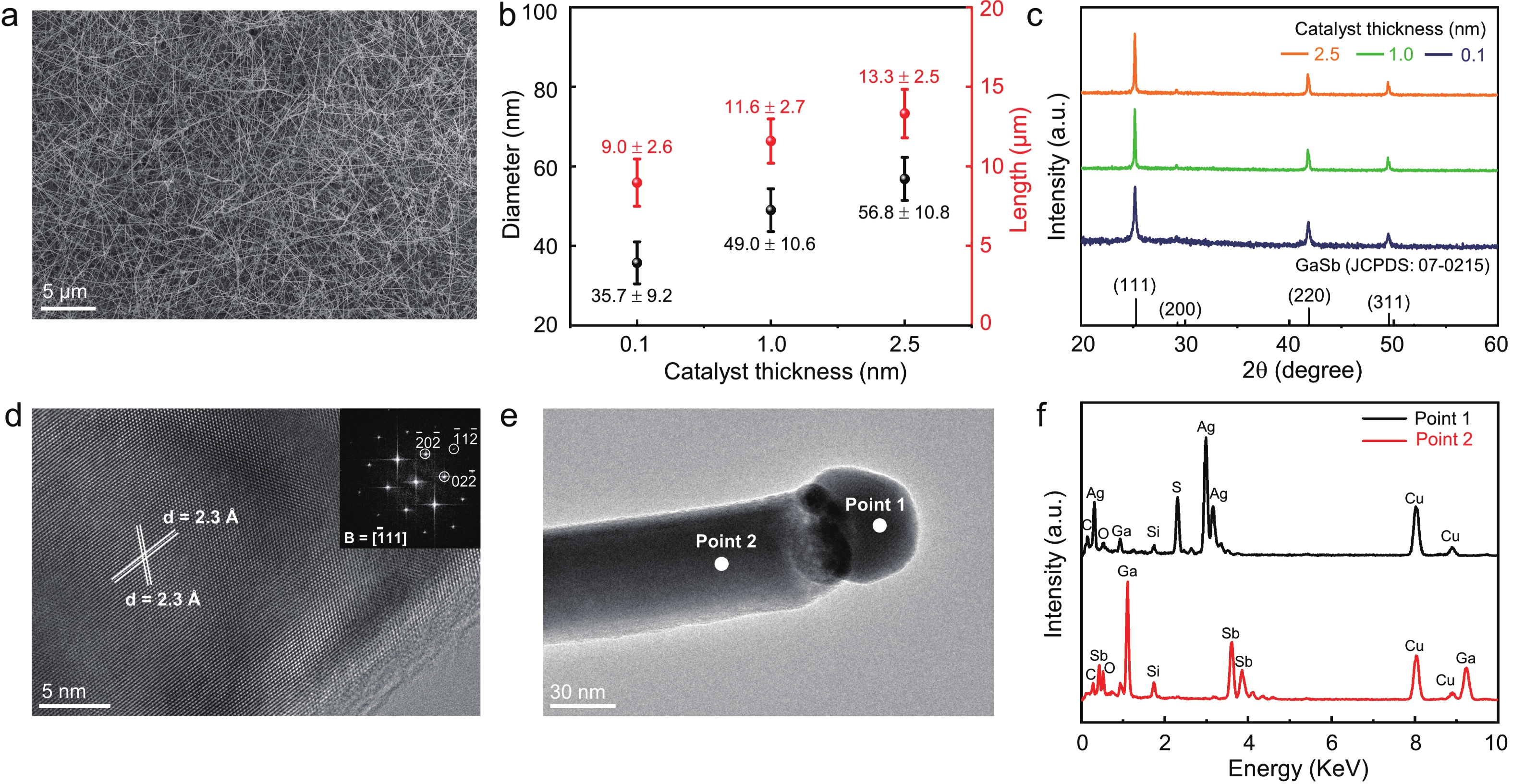
Fig. 1.  (Color online) Controllable growth of GaSb NWs by using the CMOS-compatible metal of Ag as the growth catalyst. (a–c) SEM image, diameter and length statistics, and XRD patterns of as-prepared Ag-catalyzed GaSb NWs. (d) HRTEM image of GaSb NW, insert is FFT image. (e) Scanning TEM image of an individual GaSb NW. (f) EDS of NW tip and body.

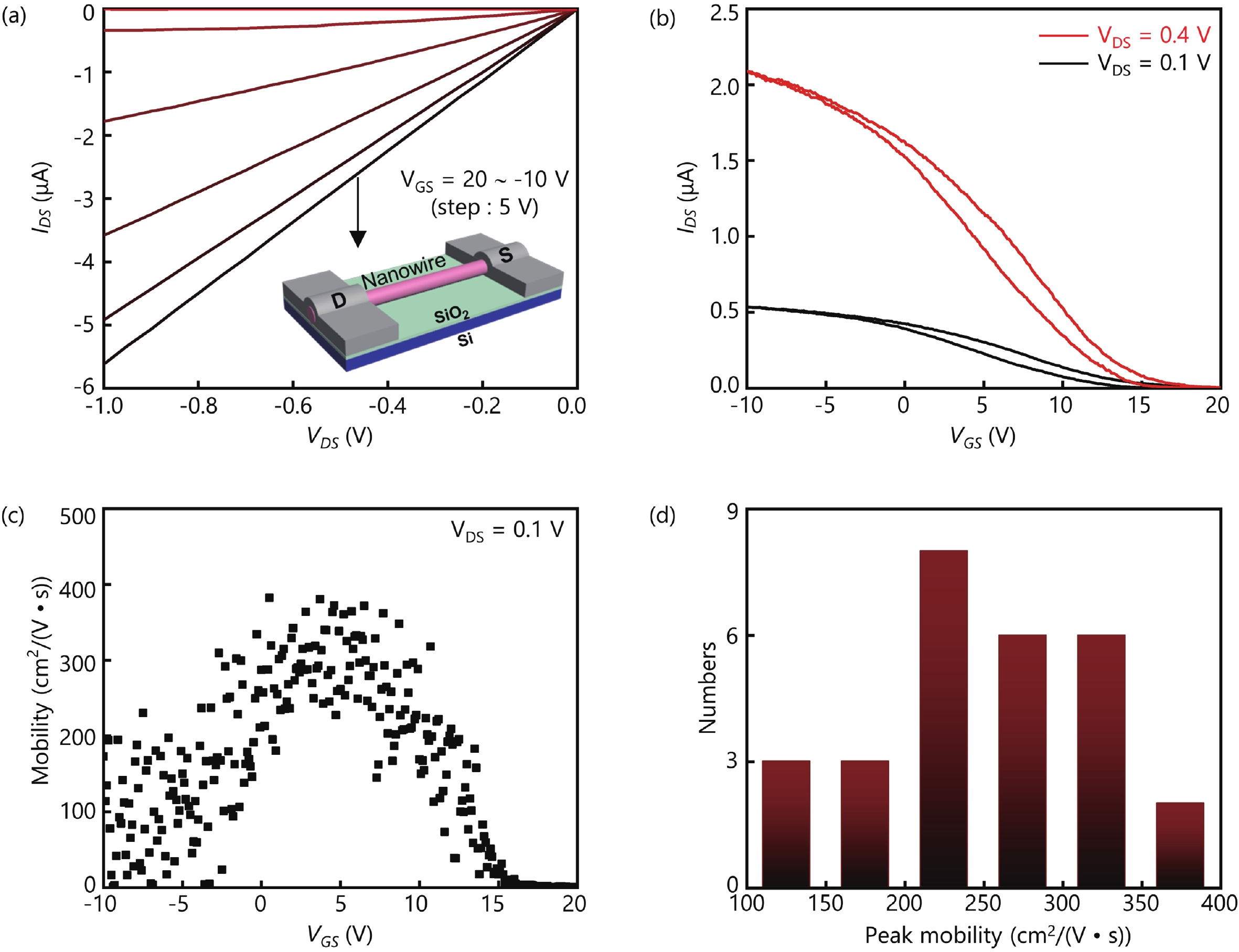
Fig. 2.  (Color online) Electrical properties of the as-prepared Ag-catalyzed GaSb NWs. (a, b) Output and transfer characteristics of as-constructed GaSb NWFET. The inset is the corresponding device schematics. (c) Hole mobility of the corresponding NWFET. (d) Peak hole mobility statistic of as-constructed NWFETs.

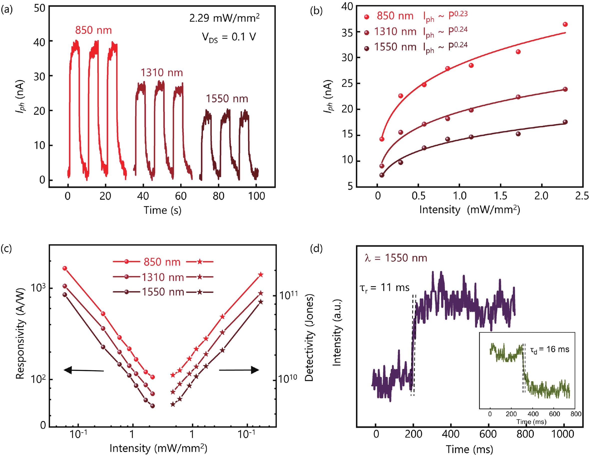
Fig. 3.  (Color online) NIR photodetection behaviors of as-prepared Ag-catalyzed GaSb NWs. (a) I–t curves of GaSb photodetector under different illuminations of λ = 850 nm to λ = 1550 nm at 0.1 V. (b, c) Incident light intensity-dependent photocurrent, responsivity and detectivity, respectively. (d) Rise and decay time of the as-fabricated photodetector under 1550 nm laser illumination.

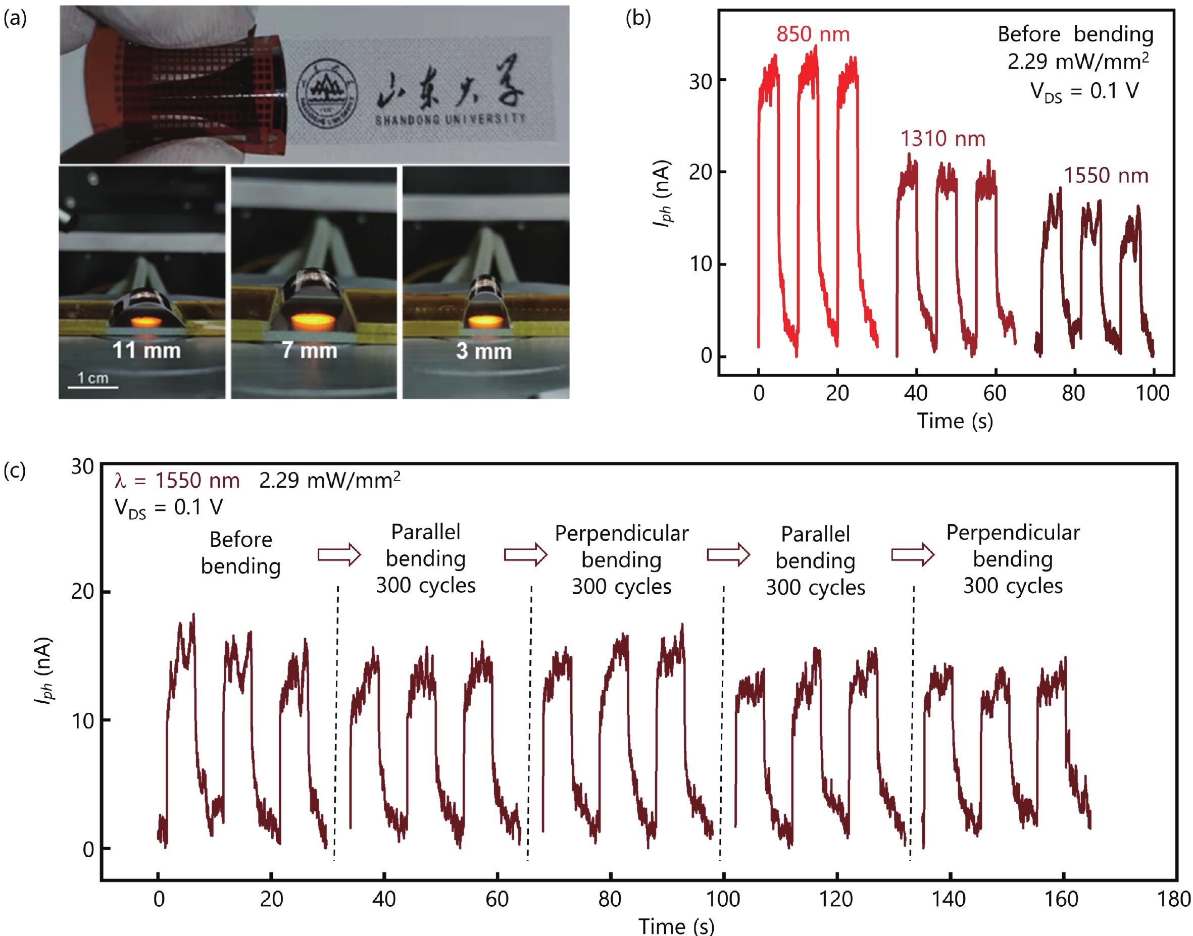
Fig. 4.  (Color online) NIR photodetection behaviors of as-fabricated GaSb NW flexible photodetector. (a) The photographs of as-fabricated flexible photodetector under different bending radius. (b) The time-resolved photoresponse of flexible photodetector under the illuminations of 850, 1310, and 1550 nm lasers with 0.1 V bias before bending. (c) The time-resolved photoresponse of photodetector under the illumination of 1550 nm laser after bending different cycles.

Table 1.   Photodetection performance comparison of GaSb NW photodetector.

GaSb NWDevices substratePhotodetection wavelength (nm)Vds (V)R (A/W)D (Jones)Response time (ms)Ref.
SingleHard15500.18518.5 × 101011/16 This work
Flexible15500.16186.7 × 1010
SingleHard80024432.8 × 10980/90 [27]
SingleHard80857225.9 × 10128700[28]
Flexible80854.9 × 1012
SingleHard1550177.31.2 × 1010[43]
SingleHard1310116005.7 × 1094.5/12 [21]
SingleHard15501618.7 × 1070.195/0.38[25]
SingleHard155019391.1 × 101150/900[44]
DownLoad: CSV
[1]
Ran W H, Wang L L, Zhao S F, et al. An integrated flexible all-nanowire infrared sensing system with record photosensitivity. Adv Mater, 2022, 32, 1908419 doi: 10.1002/adma.201908419
[2]
Wei S L, Wang F, Zou X M, et al. Flexible quasi-2D perovskite/IGZO phototransistors for ultrasensitive and broadband photodetection. Adv Mater, 2020, 32, 1907527 doi: 10.1002/adma.201907527
[3]
Li Z Y, Trendafilov S, Zhang F L, et al. Broadband GaAsSb nanowire array photodetectors for filter-free multispectral imaging. Nano Lett, 2021, 21, 7388 doi: 10.1021/acs.nanolett.1c02777
[4]
Yip S, Shen L F, Ho J C. Recent advances in flexible photodetectors based on 1D nanostructures. J Semicond, 2019, 40, 111602 doi: 10.1088/1674-4926/40/11/111602
[5]
Xie C, Yan F. Flexible photodetectors based on novel functional materials. Small 2017, 13, 1701, 822 doi: 10.1002/smll.201701822
[6]
Lou Z, Shen G Z. Flexible photodetectors based on 1D inorganic nanostructures. Adv Sci, 2016, 3, 1500287 doi: 10.1002/advs.201500287
[7]
Li P, Hao Q Y, Liu J D, et al. Flexible photodetectors based on all-solution-processed Cu electrodes and InSe nanoflakes with high stabilities. Adv Funct Mater, 2021, 32, 2108261 doi: 10.1002/adfm.202108261
[8]
Li J, Wang Z X, Chu J W, et al. Oriented layered Bi2O2Se nanowire arrays for ultrasensitive photodetectors. Appl Phys Lett, 2019, 114, 151104 doi: 10.1063/1.5094192
[9]
Wu D J, Zhou H, Song Z H, et al. Welding perovskite nanowires for stable, sensitive, flexible photodetectors. ACS Nano, 2020, 14, 2777 doi: 10.1021/acsnano.9b09315
[10]
Tao J Y, Xiao Z J, Wang J F, et al. A self-powered, flexible photodetector based on perovskite nanowires with Ni-Al electrodes. J Alloys Compd, 2020, 845, 155311 doi: 10.1016/j.jallcom.2020.155311
[11]
Lou Z, Yang X L, Chen H R, et al. Flexible ultraviolet photodetectors based on ZnO–SnO2 heterojunction nanowire arrays. J Semicond, 2018, 39, 024002 doi: 10.1088/1674-4926/39/2/024002
[12]
Li D P, Yip S, Li F Z, et al. Flexible near-infrared InGaSb nanowire array detectors with ultrafast photoconductive response below 20 µs. Adv Opt Mater, 2020, 8, 2001201 doi: 10.1002/adom.202001201
[13]
Rezaei M, Bianconi S, Lauhon L, et al. A new approach to designing high-sensitivity low-dimensional photodetectors. Nano Lett, 2021, 21, 9838 doi: 10.1021/acs.nanolett.1c03665
[14]
Barrigon E, Heurlin M, Bi Z, et al. Synthesis and applications of III-V nanowires. Chem Rev, 2019, 119, 9170 doi: 10.1021/acs.chemrev.9b00075
[15]
Yuan X M, Pan D, Zhou Y J, et al. Selective area epitaxy of III–V nanostructure arrays and networks: growth, applications, and future directions. Appl Phys Rev, 2021, 8, 021302 doi: 10.1063/5.0044706
[16]
Zuo X R, Li Z Y, Wong W W, et al. Design of InAs nanosheet arrays with ultrawide polarization-independent high absorption for infrared photodetection. Appl Phys Lett, 2022, 120, 071109 doi: 10.1063/5.0066507
[17]
Zhong Z Q, Li X L, Wu J, et al. Wavelength-tunable InAsP quantum dots in InP nanowires. Appl Phys Lett, 2019, 115, 053101 doi: 10.1063/1.5095675
[18]
Ji X H, Yang X G, Yang T. Self-catalyzed growth of vertical GaSb nanowires on InAs stems by metal-organic chemical vapor deposition. Nanoscale Res Lett, 2017, 12, 428 doi: 10.1186/s11671-017-2207-5
[19]
Wen L J, Pan D, Liao D X, et al. Foreign-catalyst-free GaSb nanowires directly grown on cleaved Si substrates by molecular-beam epitaxy. Nanotechnology, 2020, 31, 155601 doi: 10.1088/1361-6528/ab5d78
[20]
Jeppsson M, Dick K A, Nilsson H A, et al. Characterization of GaSb nanowires grown by MOVPE. J Cryst Growth, 2008, 310, 5119 doi: 10.1016/j.jcrysgro.2008.07.061
[21]
Yin Y X, Guo Y N, Liu D, et al. Substrate-free chemical vapor deposition of large-scale Ⅲ-Ⅴ nanowires for high-performance transistors and broad-spectrum photodetectors. Adv Opt Mater, 2022, 10, 2102291 doi: 10.1002/adom.202102291
[22]
Yang Z X, Han N, Fang M, et al. Surfactant-assisted chemical vapour deposition of high-performance small-diameter GaSb nanowires. Nat Commun, 2014, 5, 5249 doi: 10.1038/ncomms6249
[23]
Yang Z X, Yin Y X, Sun J M, et al. Chalcogen passivation: an in-situ method to manipulate the morphology and electrical property of GaAs nanowires. Sci Rep, 2018, 8, 6928 doi: 10.1038/s41598-018-25209-x
[24]
Yang Z X, Liu L Z, Yip S, et al. Complementary metal oxide semiconductor-compatible, high-mobility, 111-oriented GaSb nanowires enabled by vapor-solid-solid chemical vapor deposition. ACS Nano, 2017, 11, 4237 doi: 10.1021/acsnano.7b01217
[25]
Sun J M, Peng M, Zhang Y S, et al. Ultrahigh hole mobility of Sn-catalyzed GaSb nanowires for high speed infrared photodetectors. Nano Lett, 2019, 19, 5920 doi: 10.1021/acs.nanolett.9b01503
[26]
Han N, Wang Y, Yang Z X, et al. Controllable Ⅲ-Ⅴ nanowire growth via catalyst epitaxy. J Mater Chem C, 2017, 5, 4393 doi: 10.1039/C7TC00900C
[27]
Luo T, Liang B, Liu Z, et al. Single-GaSb-nanowire-based room temperature photodetectors with broad spectral response. Sci Bull, 2015, 60, 101 doi: 10.1007/s11434-014-0687-6
[28]
Zhang K, Chai R Q, Shi R L, et al. Self-catalyzed growth of GaSb nanowires for high performance ultraviolet-visible-near infrared photodetectors. Sci China Mater, 2019, 63, 383 doi: 10.1007/s40843-019-1189-7
[29]
Sun J M, Zhuang X M, Fan Y B, et al. Toward unusual-high hole mobility of p-channel field-effect-transistors. Small, 2021, 17, 2102323 doi: 10.1002/smll.202102323
[30]
Liu D, Liu F J, Liu Y, et al. Schottky-contacted high-performance GaSb nanowires photodetectors enabled by lead-free all-inorganic perovskites decoration. Small, 2022, 18, 2200415 doi: 10.1002/smll.202200415
[31]
Miao J S, Hu W D, Guo N, et al. Single InAs nanowire room-temperature near-infrared photodetectors. ACS Nano, 2014, 8, 3628 doi: 10.1021/nn500201g
[32]
Al-Zahrani S, Pal J, Migliorato M A, et al. Piezoelectric field enhancement in III-V core–shell nanowires. Nano Energy, 2015, 14, 382 doi: 10.1016/j.nanoen.2014.11.046
[33]
Holmer J, Zeng L, Kanne T, et al. Enhancing the nir photocurrent in single GaAs nanowires with radial p-i-n junctions by uniaxial strain. Nano Lett, 2021, 21, 9038 doi: 10.1021/acs.nanolett.1c02468
[34]
Ford A C, Ho J C, Chueh Y L, et al. Diameter-dependent electron mobility of InAs nanowires. Nano Lett, 2009, 9, 360 doi: 10.1021/nl803154m
[35]
Burke R A, Weng X J, Kuo M W, et al. Growth and characterization of unintentionally doped GaSb nanowires. J Electron Mater, 2010, 39, 355 doi: 10.1007/s11664-010-1140-5
[36]
Kranzer D. Mobility of holes of zinc-blende III-V and II-VI compounds. Phys Status Solidi A, 1974, 26, 11 doi: 10.1002/pssa.2210260102
[37]
Jie J S, Zhang W J, Jiang Y, at al. Photoconductive characteristics of single-crystal CdS nanoribbons. Nano Lett, 2006, 6, 1887 doi: 10.1021/nl060867g
[38]
Fang H H, Hu W D, Wang P, et al. Visible light-assisted high-performance mid-infrared photodetectors based on single InAs nanowire. Nano Lett, 2016, 16, 6416 doi: 10.1021/acs.nanolett.6b02860
[39]
Kind H, Yan H Q, Messer B, et al. Nanowire ultraviolet photodetectors and optical switches. Adv Mater, 2002, 14, 158 doi: 10.1002/1521-4095(20020116)14:2<158::AID-ADMA158>3.0.CO;2-W
[40]
Liu X, Gu L L, Zhang Q P, et al. All-printable band-edge modulated ZnO nanowire photodetectors with ultra-high detectivity. Nat Commun, 2014, 5, 4007 doi: 10.1038/ncomms5007
[41]
Zheng D S, Wang J L, Hu W D, et al. When nanowires meet ultrahigh ferroelectric field-high-performance full-depleted nanowire photodetectors. Nano Lett, 2016, 16, 2548 doi: 10.1021/acs.nanolett.6b00104
[42]
Liu L, Wu L M, Wang A W, et al. Ferroelectric-gated InSe photodetectors with high on/off ratios and photoresponsivity. Nano Lett, 2020, 20, 6666 doi: 10.1021/acs.nanolett.0c02448
[43]
Ren Z H, Wang P, Zhang K, et al. Short-wave near-infrared polarization sensitive photodetector based on GaSb nanowire. IEEE Electron Device Lett, 2021, 42, 549 doi: 10.1109/LED.2021.3061705
[44]
Zhang K, Ren Z H, Cao H C, et al. Near-infrared polarimetric image sensors based on ordered sulfur-passivation GaSb nanowire arrays. ACS Nano, 2022, 16, 8128 doi: 10.1021/acsnano.2c01455
[45]
Liu Z, Chen G, Liang B, et al. Fabrication of high-quality ZnTe nanowires toward high-performance rigid/flexible visible-light photodetectors. Opt Express, 2013, 21, 7799 doi: 10.1364/OE.21.007799
[46]
Yao Y, Huang W, Chen J H, et al. Flexible complementary circuits operating at sub-0.5V via hybrid organic-inorganic electrolyte-gated transistors. Proc Natl Acad Sci USA, 2021, 118, 44 doi: 10.1073/pnas.2111790118

2022-112302.pdf

  • Search

    Advanced Search >>

    GET CITATION

    shu

    Export: BibTex EndNote

    Article Metrics

    Article views: 962 Times PDF downloads: 85 Times Cited by: 0 Times

    History

    Received: 13 May 2022 Revised: 09 June 2022 Online: Accepted Manuscript: 12 August 2022Uncorrected proof: 15 August 2022Published: 01 November 2022

    Catalog

      Email This Article

      User name:
      Email:*请输入正确邮箱
      Code:*验证码错误
      Zixu Sa, Fengjing Liu, Dong Liu, Mingxu Wang, Jie Zhang, Yanxue Yin, Zhiyong Pang, Xinming Zhuang, Peng Wang, Zaixing Yang. Ag-catalyzed GaSb nanowires for flexible near-infrared photodetectors[J]. Journal of Semiconductors, 2022, 43(11): 112302. doi: 10.1088/1674-4926/43/11/112302 ****Zixu Sa, Fengjing Liu, Dong Liu, Mingxu Wang, Jie Zhang, Yanxue Yin, Zhiyong Pang, Xinming Zhuang, Peng Wang, Zaixing Yang. 2022: Ag-catalyzed GaSb nanowires for flexible near-infrared photodetectors. Journal of Semiconductors, 43(11): 112302. doi: 10.1088/1674-4926/43/11/112302
      Citation:
      Zixu Sa, Fengjing Liu, Dong Liu, Mingxu Wang, Jie Zhang, Yanxue Yin, Zhiyong Pang, Xinming Zhuang, Peng Wang, Zaixing Yang. Ag-catalyzed GaSb nanowires for flexible near-infrared photodetectors[J]. Journal of Semiconductors, 2022, 43(11): 112302. doi: 10.1088/1674-4926/43/11/112302 ****
      Zixu Sa, Fengjing Liu, Dong Liu, Mingxu Wang, Jie Zhang, Yanxue Yin, Zhiyong Pang, Xinming Zhuang, Peng Wang, Zaixing Yang. 2022: Ag-catalyzed GaSb nanowires for flexible near-infrared photodetectors. Journal of Semiconductors, 43(11): 112302. doi: 10.1088/1674-4926/43/11/112302

      Ag-catalyzed GaSb nanowires for flexible near-infrared photodetectors

      doi: 10.1088/1674-4926/43/11/112302
      More Information
      • Zixu Sa:got his BS from ShanDong Normal University in 2021. Now he is a MS student at Shandong University under the supervision of Prof. Zaixing Yang. His research focuses on low-dimension semiconductor device
      • Zaixing Yang:got his PhD degree in 2012 at Nanjing University. Then he joined City University of Hong Kong as a postdoc. In October 2016, he joined Shandong University as a full professor. His research interest includes low-dimensional optoelectronic materials and devices
      • Corresponding author: pang@sdu.edu.cnphywangp@sdust.edu.cnzaixyang@sdu.edu.cn
      • Received Date: 2022-05-13
      • Revised Date: 2022-06-09
      • Available Online: 2022-08-12

      Catalog

        /

        DownLoad:  Full-Size Img  PowerPoint
        Return
        Return