| Citation: |
Guang Yang, Hao Luo, Jiajun Li, Qinqin Shao, Yazhe Wang, Ruzhong Zhu, Xi Zhang, Lihui Song, Yiqiang Zhang, Lingbo Xu, Can Cui, Xiaodong Pi, Deren Yang, Rong Wang. Discrimination of dislocations in 4H-SiC by inclination angles of molten-alkali etched pits[J]. Journal of Semiconductors, 2022, 43(12): 122801. doi: 10.1088/1674-4926/43/12/122801
****
G Yang, H Luo, J J Li, Q Q Shao, Y Z Wang, R Z Zhu, X Zhang, L H Song, Y Q Zhang, L B Xu, C Cui, X D Pi, D R Yang, R Wang. Discrimination of dislocations in 4H-SiC by inclination angles of molten-alkali etched pits[J]. J. Semicond, 2022, 43(12): 122801. doi: 10.1088/1674-4926/43/12/122801
|
Discrimination of dislocations in 4H-SiC by inclination angles of molten-alkali etched pits
DOI: 10.1088/1674-4926/43/12/122801
More Information
-
Abstract
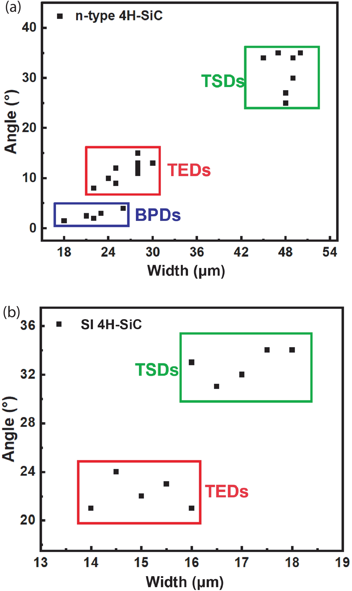
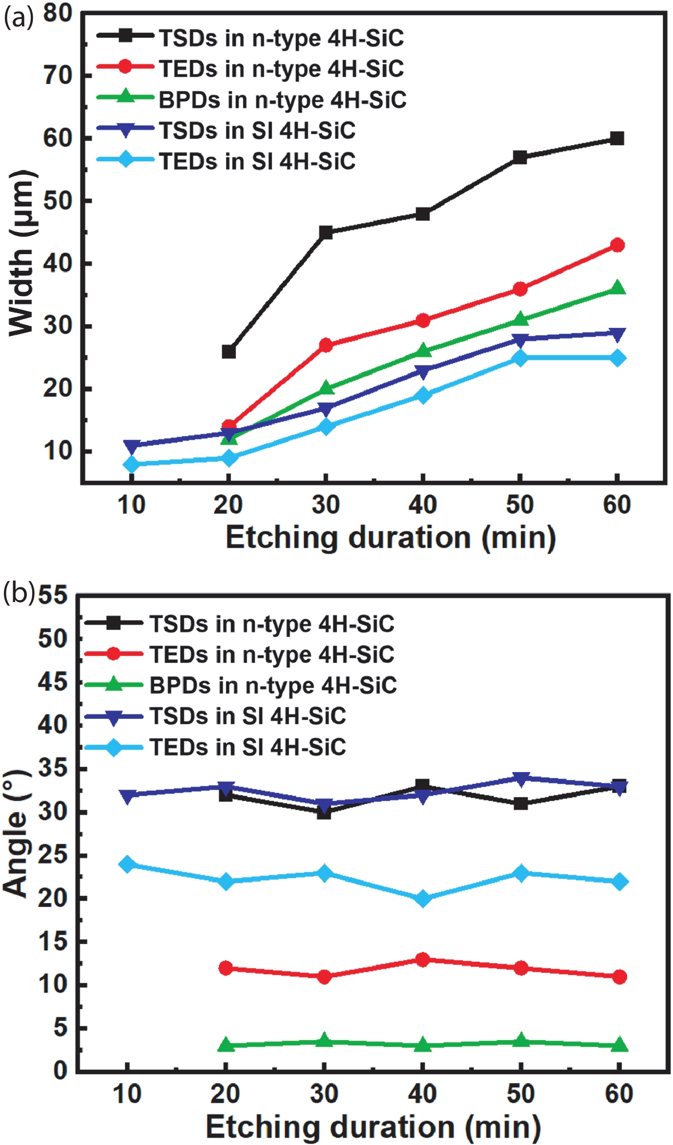
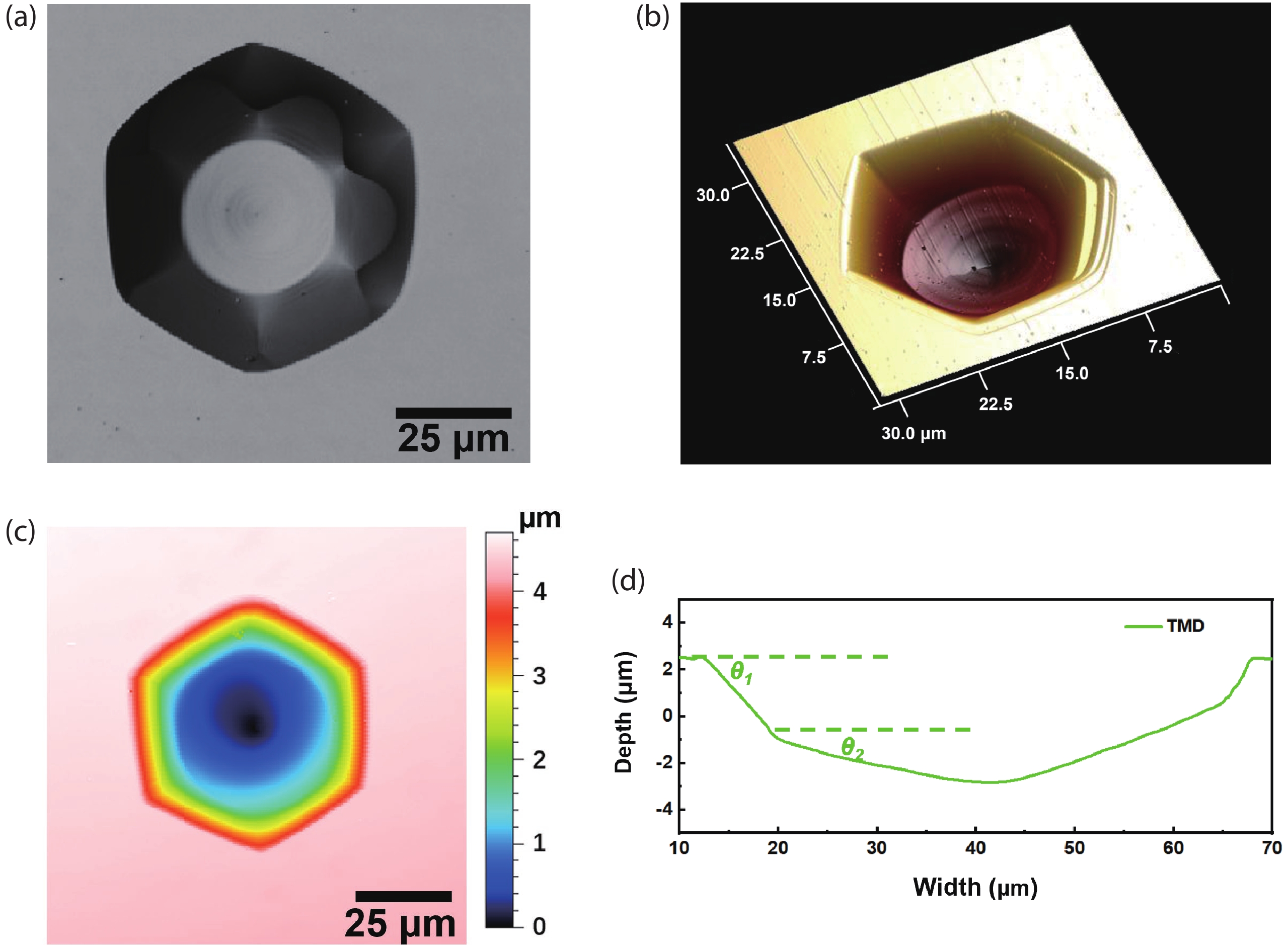
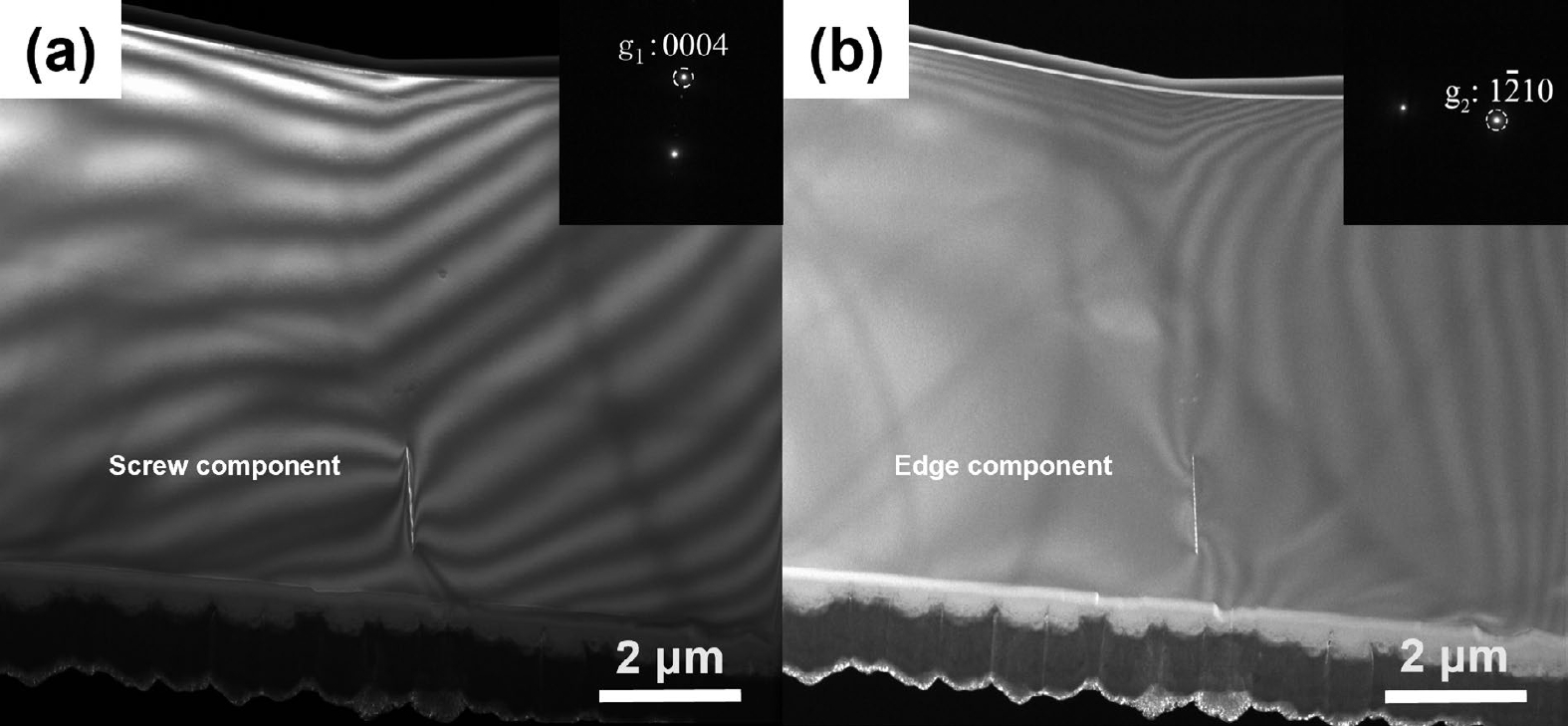
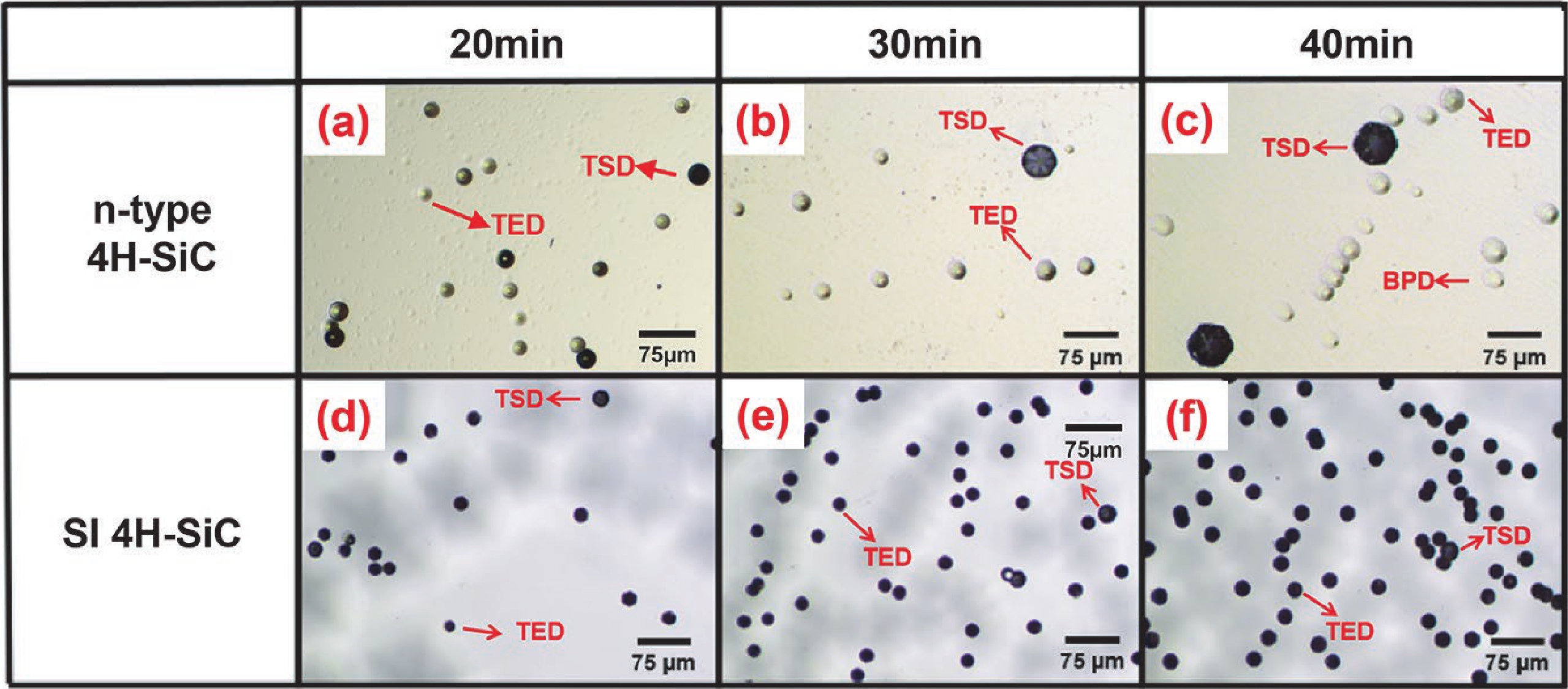
Discrimination of dislocations is critical to the statistics of dislocation densities in 4H silicon carbide (4H-SiC), which are routinely used to evaluate the quality of 4H-SiC single crystals and homoepitaxial layers. In this work, we show that the inclination angles of the etch pits of molten-alkali etched 4H-SiC can be adopted to discriminate threading screw dislocations (TSDs), threading edge dislocations (TEDs) and basal plane dislocations (BPDs) in 4H-SiC. In n-type 4H-SiC, the inclination angles of the etch pits of TSDs, TEDs and BPDs in molten-alkali etched 4H-SiC are in the ranges of 27°−35°, 8°−15° and 2°−4°, respectively. In semi-insulating 4H-SiC, the inclination angles of the etch pits of TSDs and TEDs are in the ranges of 31°−34° and 21°−24°, respectively. The inclination angles of dislocation-related etch pits are independent of the etching duration, which facilitates the discrimination and statistic of dislocations in 4H-SiC. More significantly, the inclination angle of a threading mixed dislocations (TMDs) is found to consist of characteristic angles of both TEDs and TSDs. This enables to distinguish TMDs from TSDs in 4H-SiC.-
Keywords:
- 4H-SiC single crystals,
- dislocations,
- molten-alkali etching
-
References
[1] Casady J B, Johnson R W. Status of silicon carbide (SiC) as a wide-bandgap semiconductor for high-temperature applications: A review. Solid State Electron, 1996, 39, 1409 doi: 10.1016/0038-1101(96)00045-7[2] Wright N G, Horsfall A B, Vassilevski K. Prospects for SiC electronics and sensors. Mater Today, 2008, 11, 16 doi: 10.1016/S1369-7021(07)70348-6[3] Yoon J, Kim K. A 3.3 kV 4H-SiC split gate MOSFET with a central implant region for superior trade-off between static and switching performance. J Semicond, 2021, 42, 062803 doi: 10.1088/1674-4926/42/6/062803[4] Yeo I G, Yang W S, Park J H, et al. Two-inch a-plane (11-20) 6H-SiC crystal grown by using the PVT method from a small rectangular substrate. J Korean Phy Soc, 2011, 58, 1541 doi: 10.3938/jkps.58.1541[5] She X, Huang A Q, Lucía Ó, et al. Review of silicon carbide power devices and their applications. IEEE Trans Ind Electron, 2017, 64, 8193 doi: 10.1109/TIE.2017.2652401[6] Wang X, Zhong Y W, Pu H B, et al. Investigation of lateral spreading current in the 4H-SiC Schottky barrier diode chip. J Semicond, 2021, 42, 112802 doi: 10.1088/1674-4926/42/11/112802[7] Lukin D M, Dory C, Guidry M A, et al. 4H-silicon-carbide-on-insulator for integrated quantum and nonlinear photonics. Nat Photonics, 2020, 14, 330 doi: 10.1038/s41566-019-0556-6[8] von Bardeleben H J, Cantin J L, Csóré A, et al. NV centers in 3C, 4H, and 6H silicon carbide: A variable platform for solid-state qubits and nanosensors. Phys Rev B, 2016, 94, 121202 doi: 10.1103/PhysRevB.94.121202[9] Banks H B, Soykal Ö O, Myers-Ward R L, et al. Resonant optical spin initialization and readout of single silicon vacancies in 4H-SiC. Phys Rev Appl, 2019, 11, 024013 doi: 10.1103/PhysRevApplied.11.024013[10] Wang J F, Yan F F, Li Q, et al. Coherent control of nitrogen-vacancy center spins in silicon carbide at room temperature. Phys Rev Lett, 2020, 124, 223601 doi: 10.1103/PhysRevLett.124.223601[11] Wang J F, Yan F F, Li Q, et al. Robust coherent control of solid-state spin qubits using anti-Stokes excitation. Nat Commun, 2021, 12, 3223 doi: 10.1038/s41467-021-23471-8[12] Ha S, Benamara M, Skowronski M, et al. Core structure and properties of partial dislocations in silicon carbide p-i-n diodes. Appl Phys Lett, 2003, 83, 4957 doi: 10.1063/1.1633969[13] Abadier M, Myers-Ward R L, Mahadik N A, et al. Nucleation of in-grown stacking faults and dislocation half-loops in 4H-SiC epitaxy. J Appl Phys, 2013, 114, 123502 doi: 10.1063/1.4821242[14] Wahab Q, Ellison A, Henry A, et al. Influence of epitaxial growth and substrate-induced defects on the breakdown of 4H-SiC Schottky diodes. Appl Phys Lett, 2000, 76, 2725 doi: 10.1063/1.126456[15] Neudeck P G, Powell J A. Performance limiting micropipe defects in silicon carbide wafers. IEEE Electron Device Lett, 1994, 15, 63 doi: 10.1109/55.285372[16] Grekov A, Zhang Q C, Fatima H, et al. Effect of crystallographic defects on the reverse performance of 4H-SiC JBS diodes. Microelectron Reliab, 2008, 48, 1664 doi: 10.1016/j.microrel.2008.05.001[17] Neudeck P G, Huang W, Dudley M. Study of bulk and elementary screw dislocation assisted reverse breakdown in low-voltage (<250 V) 4H-SiC p+n junction diodes. I. DC properties. IEEE Trans Electron Devices, 1999, 46, 478 doi: 10.1109/16.748865[18] Stahlbush R E, Twigg M E, Sumakeris J J, et al. Mechanisms of stacking fault growth in SiC PiN diodes. MRS Online Proc Libr, 2004, 815, 241 doi: 10.1557/PROC-815-J6.4[19] Ha S, Chung H J, Nuhfer N T, et al. Dislocation nucleation in 4H silicon carbide epitaxy. J Cryst Growth, 2004, 262, 130 doi: 10.1016/j.jcrysgro.2003.09.054[20] Zhuang D, Edgar J H. Wet etching of GaN, AlN, and SiC: a review. Mater Sci Eng R, 2005, 48, 1 doi: 10.1016/j.mser.2004.11.002[21] Christiansen K, Helbig R. Anisotropic oxidation of 6H-SiC. J Appl Phys, 1996, 79, 3276 doi: 10.1063/1.361225[22] Geng W, Yang G, Zhang X, et al. Identification of subsurface damages of 4H-SiC wafers by combining photo-chemical etching and molten-alkali etching. J Semicond, 2022, 43, 102801 doi: 10.1088/1674-4926/43/10/102801[23] Brander R W, Boughey A L. The etching of-silicon carbide. Br J Appl Phys, 1967, 18, 905 doi: 10.1088/0508-3443/18/7/304[24] Dong L, Zheng L, Liu X F, et al. Defect revelation and evaluation of 4H silicon carbide by optimized molten KOH etching method. Mater Sci Forum, 2013, 740, 243 doi: 10.4028/www.scientific.net/MSF.740-742.243[25] Li J J, Luo H, Yang G, et al. Nitrogen decoration of basal-plane dislocations in 4H-SiC. Phys Rev Appl, 2022, 17, 054011 doi: 10.1103/PhysRevApplied.17.054011[26] Katsuno M, Ohtani N, Takahashi J, et al. Mechanism of molten KOH etching of SiC single crystals: Comparative study with thermal oxidation. Jpn J Appl Phys, 1999, 38, 4661 doi: 10.1143/JJAP.38.4661[27] Sakwe S A, Müller R, Wellmann P J. Optimization of KOH etching parameters for quantitative defect recognition in n- and p-type doped SiC. J Cryst Growth, 2006, 289, 520 doi: 10.1016/j.jcrysgro.2005.11.096[28] Yao Y Z, Ishikawa Y, Sugawara Y, et al. Molten KOH etching with Na2O2 additive for dislocation revelation in 4H-SiC epilayers and substrates. Jpn J Appl Phys, 2011, 50, 075502 doi: 10.1143/JJAP.50.075502[29] Siche D, Klimm D, Hölzel T, et al. Reproducible defect etching of SiC single crystals. J Cryst Growth, 2004, 270, 1 doi: doi.org/10.1016/j.jcrysgro.2004.05.098[30] Yang Y, Chen Z Z. Defect characterization of SiC by wet etching process. J Synth Cryst, 2008, 37, 634 doi: 10.16553/j.cnki.issn1000-985x.2008.03.051[31] Song H Z, Sudarshan T S. Basal plane dislocation mitigation in SiC epitaxial growth by nondestructive substrate treatment. Cryst Growth Des, 2012, 12, 1703 doi: 10.1021/cg300077g[32] Luo H, Li J J, Yang G, et al. Electronic and optical properties of threading dislocations in n-type 4H-SiC. ACS Appl Electron Mater, 2022, 4, 1678 doi: 10.1021/acsaelm.1c01330[33] Takahashi J, Kanaya M, Fujiwara Y. Sublimation growth of SiC single crystalline ingots on faces perpendicular to the (0001) basal plane. J Cryst Growth, 1994, 135, 61 doi: 10.1016/0022-0248(94)90726-9[34] Gao Y, Zhang Z H, Bondokov R, et al. The effect of doping concentration and conductivity type on preferential etching of 4H-SiC by molten KOH. MRS Online Proc Libr, 2004, 815, 6 doi: https://doi.org/10.1557/PROC-815-J5.20[35] Zhang Y, Chen H, Liu D Z, et al. High efficient polishing of sliced 4H-SiC (0001) by molten KOH etching. Appl Surf Sci, 2020, 525, 146532 doi: 10.1016/j.apsusc.2020.146532[36] Cui Y X, Hu X B, Xie X J, et al. Threading dislocation classification for 4H-SiC substrates using the KOH etching method. CrystEngComm, 2018, 20, 978 doi: 10.1039/C7CE01855J[37] Nakamura D, Yamaguchi S, Gunjishima I, et al. Topographic study of dislocation structure in hexagonal SiC single crystals with low dislocation density. J Cryst Growth, 2007, 304, 57 doi: 10.1016/j.jcrysgro.2007.02.002[38] Konishi K, Nakamura Y, Nagae A, et al. Direct observation and three dimensional structural analysis for threading mixed dislocation inducing current leakage in 4H-SiC IGBT. Jpn J Appl Phys, 2020, 59, 011001 doi: 10.7567/1347-4065/ab5ee8[39] Yao Y Z, Ishikawa Y, Sugawara Y, et al. Correlation between etch pits formed by molten KOH+Na2O2 etching and dislocation types in heavily doped n+-4H-SiC studied by X-ray topography. J Cryst Growth, 2013, 364, 7 doi: 10.1016/j.jcrysgro.2012.12.011[40] Fukunaga K, Jun S D, Kimoto T. Anisotropic etching of single crystalline SiC using molten KOH for SiC bulk micromachining. Micromachining and Microfabrication Process Technology XI, 2006 doi: https://doi.org/10.1117/12.647116[41] Katsuno T, Watanabe Y, Hirokazu F, et al. New separation method of threading dislocations in 4H-SiC epitaxial layer by molten KOH etching. Mater Sci Forum, 2011, 679/680, 298 doi: 10.4028/www.scientific.net/MSF.679-680.298 -
Proportional views


 DownLoad:
