J. Semicond. > 2022, Volume 43 > Issue 2 > 022101

ARTICLES

Defects properties and vacancy diffusion in Cu2MgSnS4

Kin Fai Tse, Shengyuan Wang, Man Hoi Wong and Junyi Zhu

+ Author Affiliations

 Corresponding author: Junyi Zhu, jyzhu@phy.cuhk.edu.hk

DOI: 10.1088/1674-4926/43/2/022101

PDF

Turn off MathJax

Abstract: Cu2ZnSnS4 (CZTS) is a promising photovoltaic absorber material, however, efficiency is largely hindered by potential fluctuation and a band tailing problem due to the abundance of defect complexes and low formation energy of an intrinsic CuZn defect. Alternatives to CZTS by group I, II, or IV element replacement to circumvent this challenge has grown research interest. In this work, using a hybrid (HSE06) functional, we demonstrated the qualitative similarity of defect thermodynamics and electronic properties in Cu2MgSnS4 (CMTS) to CZTS. We show SnMg to be abundant when in Sn- and Cu-rich condition, which can be detrimental, while defect properties are largely similar to CZTS in Sn- and Cu-poor. Under Sn- and Cu-poor chemical potential, there is a general increase in formation energy in most defects except SnMg, CuMg remains as the main contribution to p-type carriers, and SnMg may be detrimental because of a deep defect level in the mid gap and the possibility of forming defect complex SnMg+MgSn. Vacancy diffusion is studied using generalized gradient approximation, and we find similar vacancy diffusion properties for Cu vacancy and lower diffusion barrier for Mg vacancy, which may reduce possible Cu-Mg disorder in CMTS. These findings further confirm the feasibility of CMTS as an alternative absorber material to CZTS and suggest the possibility for tuning defect properties of CZTS, which is crucial for high photovoltaic performance.

Key words: CMTSCZTSdefecthybrid functionaldiffusion


[1]
Chen S Y, Gong X G, Walsh A, et al. Crystal and electronic band structure of Cu2ZnSnX4 (X = S and Se) photovoltaic absorbers: First-principles insights. Appl Phys Lett, 2009, 94, 041903 doi: 10.1063/1.3074499
[2]
He J, Sun L, Chen S Y, et al. Composition dependence of structure and optical properties of Cu2ZnSn(S, Se)4 solid solutions: An experimental study. J Alloys Compd, 2012, 511, 129 doi: 10.1016/j.jallcom.2011.08.099
[3]
Levcenco S, Dumcenco D, Wang Y P, et al. Influence of anionic substitution on the electrolyte electroreflectance study of band edge transitions in single crystal Cu2ZnSn(S xSe1− x)4 solid solutions. Opt Mater, 2012, 34, 1362 doi: 10.1016/j.optmat.2012.02.028
[4]
Persson C. Electronic and optical properties of Cu2ZnSnS4 and Cu2ZnSnSe4. J Appl Phys, 2010, 107, 053710 doi: 10.1063/1.3318468
[5]
Wang W, Winkler M T, Gunawan O, et al. Device characteristics of CZTSSe thin-film solar cells with 12.6% efficiency. Adv Energy Mater, 2014, 4, 1301465 doi: 10.1002/aenm.201301465
[6]
Yan C, Huang J L, Sun K W, et al. Cu2ZnSnS4 solar cells with over 10% power conversion efficiency enabled by heterojunction heat treatment. Nat Energy, 2018, 3, 764 doi: 10.1038/s41560-018-0206-0
[7]
Liu X L, Feng Y, Cui H T, et al. The current status and future prospects of kesterite solar cells: A brief review. Prog Photovolt: Res Appl, 2016, 24, 879 doi: 10.1002/pip.2741
[8]
Bishop D M, McCandless B, Gershon T, et al. Modification of defects and potential fluctuations in slow-cooled and quenched Cu2ZnSnSe4 single crystals. J Appl Phys, 2017, 121, 065704 doi: 10.1063/1.4975483
[9]
Zhuk S, Kushwaha A, Wong T K S, et al. Critical review on sputter-deposited Cu2ZnSnS4 (CZTS) based thin film photovoltaic technology focusing on device architecture and absorber quality on the solar cells performance. Sol Energy Mater Sol Cells, 2017, 171, 239 doi: 10.1016/j.solmat.2017.05.064
[10]
Gunawan O, Todorov T K, Mitzi D B. Loss mechanisms in hydrazine-processed Cu2ZnSn(Se, S)4 solar cells. Appl Phys Lett, 2010, 97, 233506 doi: 10.1063/1.3522884
[11]
Han D, Sun Y Y, Bang J, et al. Deep electron traps and origin of p-type conductivity in the earth-abundant solar-cell material Cu2ZnSnS4. Phys Rev B, 2013, 87, 155206 doi: 10.1103/PhysRevB.87.155206
[12]
Chen S Y, Walsh A, Gong X G, et al. Classification of lattice defects in the kesterite Cu2ZnSnS4 and Cu2ZnSnSe4 earth-abundant solar cell absorbers. Adv Mater, 2013, 25, 1522 doi: 10.1002/adma.201203146
[13]
Gokmen T, Gunawan O, Todorov T K, et al. Band tailing and efficiency limitation in kesterite solar cells. Appl Phys Lett, 2013, 103, 103506 doi: 10.1063/1.4820250
[14]
Romero M J, Du H, Teeter G, et al. Comparative study of the luminescence and intrinsic point defects in the kesterite Cu2ZnSnS4 and chalcopyrite Cu(In, Ga)Se2 thin films used in photovoltaic applications. Phys Rev B, 2011, 84, 165324 doi: 10.1103/PhysRevB.84.165324
[15]
Rey G, Larramona G, Bourdais S, et al. On the origin of band-tails in kesterite. Sol Energy Mater Sol Cells, 2018, 179, 142 doi: 10.1016/j.solmat.2017.11.005
[16]
Li J J, Wang D X, Li X L, et al. Cation substitution in earth-abundant kesterite photovoltaic materials. Adv Sci, 2018, 5, 1700744 doi: 10.1002/advs.201700744
[17]
Pal K, Singh P, Bhaduri A, et al. Current challenges and future prospects for a highly efficient (>20%) kesterite CZTS solar cell: A review. Sol Energy Mater Sol Cells, 2019, 196, 138 doi: 10.1016/j.solmat.2019.03.001
[18]
Kanevce A, Repins I, Wei S H. Impact of bulk properties and local secondary phases on the Cu2(Zn, Sn)Se4 solar cells open-circuit voltage. Sol Energy Mater Sol Cells, 2015, 133, 119 doi: 10.1016/j.solmat.2014.10.042
[19]
Kosyak V, Postnikov A V, Scragg J, et al. Calculation of point defect concentration in Cu2ZnSnS4: Insights into the high-temperature equilibrium and quenching. J Appl Phys, 2017, 122, 035707 doi: 10.1063/1.4994689
[20]
Huang D, Persson C. Band gap change induced by defect complexes in Cu2ZnSnS4. Thin Solid Films, 2013, 535, 265 doi: 10.1016/j.tsf.2012.10.030
[21]
Zawadzki P, Zakutayev A, Lany S. Entropy-driven clustering in tetrahedrally bonded multinary materials. Phys Rev Appl, 2015, 3, 034007 doi: 10.1103/PhysRevApplied.3.034007
[22]
Scragg J J S, Choubrac L, Lafond A, et al. A low-temperature order-disorder transition in Cu2ZnSnS4 thin films. Appl Phys Lett, 2014, 104, 041911 doi: 10.1063/1.4863685
[23]
Mendis B G, Goodman M C J, Major J D, et al. The role of secondary phase precipitation on grain boundary electrical activity in Cu2ZnSnS4 (CZTS) photovoltaic absorber layer material. J Appl Phys, 2012, 112, 124508 doi: 10.1063/1.4769738
[24]
Yang W C, Miskin C K, Carter N J, et al. Compositional inhomogeneity of multinary semiconductor nanoparticles: A case study of Cu2ZnSnS4. Chem Mater, 2014, 26, 6955 doi: 10.1021/cm502930d
[25]
Scragg J J, Wätjen J T, Edoff M, et al. A detrimental reaction at the molybdenum back contact in Cu2ZnSn(S, Se)4 thin-film solar cells. J Am Chem Soc, 2012, 134, 19330 doi: 10.1021/ja308862n
[26]
Scragg J J, Kubart T, Wätjen J T, et al. Effects of back contact instability on Cu2ZnSnS4 devices and processes. Chem Mater, 2013, 25, 3162 doi: 10.1021/cm4015223
[27]
Dalapati G K, Zhuk S, Masudy-Panah S, et al. Impact of molybdenum out diffusion and interface quality on the performance of sputter grown CZTS based solar cells. Sci Rep, 2017, 7, 1350 doi: 10.1038/s41598-017-01605-7
[28]
Bär M, Schubert B A, Marsen B, et al. Cliff-like conduction band offset and KCN-induced recombination barrier enhancement at the CdS/Cu2ZnSnS4 thin-film solar cell heterojunction. Appl Phys Lett, 2011, 99, 222105 doi: 10.1063/1.3663327
[29]
Nagaoka A, Miyake H, Taniyama T, et al. Effects of sodium on electrical properties in Cu2ZnSnS4 single crystal. Appl Phys Lett, 2014, 104, 152101 doi: 10.1063/1.4871208
[30]
Gershon T, Shin B, Bojarczuk N, et al. The role of sodium as a surfactant and suppressor of non-radiative recombination at internal surfaces in Cu2ZnSnS4. Adv Energy Mater, 2015, 5, 1400849 doi: 10.1002/aenm.201400849
[31]
Zhang Y O, Tse K, Xiao X D, et al. Controlling defects and secondary phases of CZTS by surfactant potassium. Phys Rev Mater, 2017, 1, 045403 doi: 10.1103/PhysRevMaterials.1.045403
[32]
Yan C, Liu F Y, Song N, et al. Band alignments of different buffer layers (CdS, Zn(O, S), and In2S3) on Cu2ZnSnS4. Appl Phys Lett, 2014, 104, 173901 doi: 10.1063/1.4873715
[33]
Sun K W, Yan C, Liu F Y, et al. Over 9% efficient kesterite Cu2ZnSnS4 solar cell fabricated by using Zn1– xCd xS buffer layer. Adv Energy Mater, 2016, 6, 1600046 doi: 10.1002/aenm.201600046
[34]
Li X L, Su Z H, Venkataraj S, et al. 8.6% Efficiency CZTSSe solar cell with atomic layer deposited Zn-Sn-O buffer layer. Sol Energy Mater Sol Cells, 2016, 157, 101 doi: 10.1016/j.solmat.2016.05.032
[35]
Li J J, Liu X R, Liu W, et al. Restraining the band fluctuation of CBD-Zn(O, S) layer: Modifying the hetero-junction interface for high performance Cu2ZnSnSe4 solar cells with Cd-free buffer layer. Sol RRL, 2017, 1, 1700075 doi: 10.1002/solr.201700075
[36]
Cui H T, Liu X L, Liu F Y, et al. Boosting Cu2ZnSnS4 solar cells efficiency by a thin Ag intermediate layer between absorber and back contact. Appl Phys Lett, 2014, 104, 041115 doi: 10.1063/1.4863951
[37]
Liu F Y, Sun K W, Li W, et al. Enhancing the Cu2ZnSnS4 solar cell efficiency by back contact modification: Inserting a thin TiB2 intermediate layer at Cu2ZnSnS4/Mo interface. Appl Phys Lett, 2014, 104, 051105 doi: 10.1063/1.4863736
[38]
Liu X L, Cui H T, Li W, et al. Improving Cu2ZnSnS4 (CZTS) solar cell performance by an ultrathin ZnO intermediate layer between CZTS absorber and Mo back contact. Phys Status Solidi RRL, 2014, 8, 966 doi: 10.1002/pssr.201409052
[39]
Tong Z F, Zhang K, Sun K W, et al. Modification of absorber quality and Mo-back contact by a thin Bi intermediate layer for kesterite Cu2ZnSnS4 solar cells. Sol Energy Mater Sol Cells, 2016, 144, 537 doi: 10.1016/j.solmat.2015.09.066
[40]
Gu Y C, Shen H P, Ye C, et al. All-solution-processed Cu2ZnSnS4 solar cells with self-depleted Na2S back contact modification layer. Adv Funct Mater, 2018, 28, 1703369 doi: 10.1002/adfm.201703369
[41]
Wang C C, Chen S Y, Yang J H, et al. Design of I2–II–IV–VI4 semiconductors through element substitution: The thermodynamic stability limit and chemical trend. Chem Mater, 2014, 26, 3411 doi: 10.1021/cm500598x
[42]
Zhong G H, Tse K, Zhang Y O, et al. Induced effects by the substitution of Zn in Cu2ZnSnX4 (X = S and Se). Thin Solid Films, 2016, 603, 224 doi: 10.1016/j.tsf.2016.02.005
[43]
Yuan Z K, Chen S Y, Xiang H J, et al. Engineering solar cell absorbers by exploring the band alignment and defect disparity: The case of Cu- and Ag-based kesterite compounds. Adv Funct Mater, 2015, 25, 6733 doi: 10.1002/adfm.201502272
[44]
Qi Y F, Kou D X, Zhou W H, et al. Engineering of interface band bending and defects elimination via a Ag-graded active layer for efficient (Cu, Ag)2ZnSn(S, Se)4 solar cells. Energy Environ Sci, 2017, 10, 2401 doi: 10.1039/C7EE01405H
[45]
Su Z H, Tan J M R, Li X L, et al. Cation substitution of solution-processed Cu2ZnSnS4 thin film solar cell with over 9% efficiency. Adv Energy Mater, 2015, 5, 1500682 doi: 10.1002/aenm.201500682
[46]
Bag S, Gunawan O, Gokmen T, et al. Hydrazine-processed Ge-substituted CZTSe solar cells. Chem Mater, 2012, 24, 4588 doi: 10.1021/cm302881g
[47]
Collord A D, Hillhouse H W. Germanium alloyed kesterite solar cells with low voltage deficits. Chem Mater, 2016, 28, 2067 doi: 10.1021/acs.chemmater.5b04806
[48]
Wei M, Du Q Y, Wang R, et al. Synthesis of new earth-abundant kesterite Cu2MgSnS4 nanoparticles by hot-injection method. Chem Lett, 2014, 43, 1149 doi: 10.1246/cl.140208
[49]
Agawane G L, Vanalakar S A, Kamble A S, et al. Fabrication of Cu2(Zn xMg1– x)SnS4 thin films by pulsed laser deposition technique for solar cell applications. Mater Sci Semicond Process, 2018, 76, 50 doi: 10.1016/j.mssp.2017.12.010
[50]
Yang G, Zhai X L, Li Y F, et al. Synthesis and characterizations of Cu2MgSnS4 thin films with different sulfuration temperatures. Mater Lett, 2019, 242, 58 doi: 10.1016/j.matlet.2019.01.102
[51]
Caballero R, Haass S G, Andres C, et al. Effect of magnesium incorporation on solution-processed kesterite solar cells. Front Chem, 2018, 6, 5 doi: 10.3389/fchem.2018.00005
[52]
Lie S, Leow S W, Bishop D M, et al. Improving carrier-transport properties of CZTS by Mg incorporation with spray pyrolysis. ACS Appl Mater Interfaces, 2019, 11, 25824 doi: 10.1021/acsami.9b05244
[53]
Chen S Y, Yang J H, Gong X G, et al. Intrinsic point defects and complexes in the quaternary kesterite semiconductor Cu2ZnSnS4. Phys Rev B, 2010, 81, 245204 doi: 10.1103/PhysRevB.81.245204
[54]
Hinuma Y, Grüneis A, Kresse G, et al. Band alignment of semiconductors from density-functional theory and many-body perturbation theory. Phys Rev B, 2014, 90, 155405 doi: 10.1103/PhysRevB.90.155405
[55]
Wei S H. Overcoming the doping bottleneck in semiconductors. Comput Mater Sci, 2004, 30, 337 doi: 10.1016/j.commatsci.2004.02.024
[56]
Freysoldt C, Neugebauer J, van de Walle C G. Fully ab initio finite-size corrections for charged-defect supercell calculations. Phys Rev Lett, 2009, 102, 016402 doi: 10.1103/PhysRevLett.102.016402
[57]
Chen S Y, Gong X G, Walsh A, et al. Electronic structure and stability of quaternary chalcogenide semiconductors derived from cation cross-substitution of II-VI and I-III-VI2 compounds. Phys Rev B, 2009, 79, 165211 doi: 10.1103/PhysRevB.79.165211
[58]
Zhu J Y, Liu F, Stringfellow G B, et al. Strain-enhanced doping in semiconductors: Effects of dopant size and charge state. Phys Rev Lett, 2010, 105, 195503 doi: 10.1103/PhysRevLett.105.195503
[59]
Hu H, Liu M, Wang Z F, et al. Quantum electronic stress: Density-functional-theory formulation and physical manifestation. Phys Rev Lett, 2012, 109, 055501 doi: 10.1103/PhysRevLett.109.055501
[60]
Noufi R, Axton R, Herrington C, et al. Electronic properties versus composition of thin films of CuInSe2. Appl Phys Lett, 1984, 45, 668 doi: 10.1063/1.95350
[61]
Xiao W, Wang J N, Zhao X S, et al. Intrinsic defects and Na doping in Cu2ZnSnS4: A density-functional theory study. Sol Energy, 2015, 116, 125 doi: 10.1016/j.solener.2015.04.005
[62]
Henkelman G, Uberuaga B P, Jónsson H. A climbing image nudged elastic band method for finding saddle points and minimum energy paths. J Chem Phys, 2000, 113, 9901 doi: 10.1063/1.1329672
[63]
Perdew J P, Burke K, Ernzerhof M. Generalized gradient approximation made simple. Phys Rev Lett, 1996, 77, 3865 doi: 10.1103/PhysRevLett.77.3865
[64]
Nakamura S, Maeda T, Wada T. First-principles study of diffusion of Cu and in atoms in CuInSe2. Jpn J Appl Phys, 2013, 52, 04CR01 doi: 10.7567/JJAP.52.04CR01
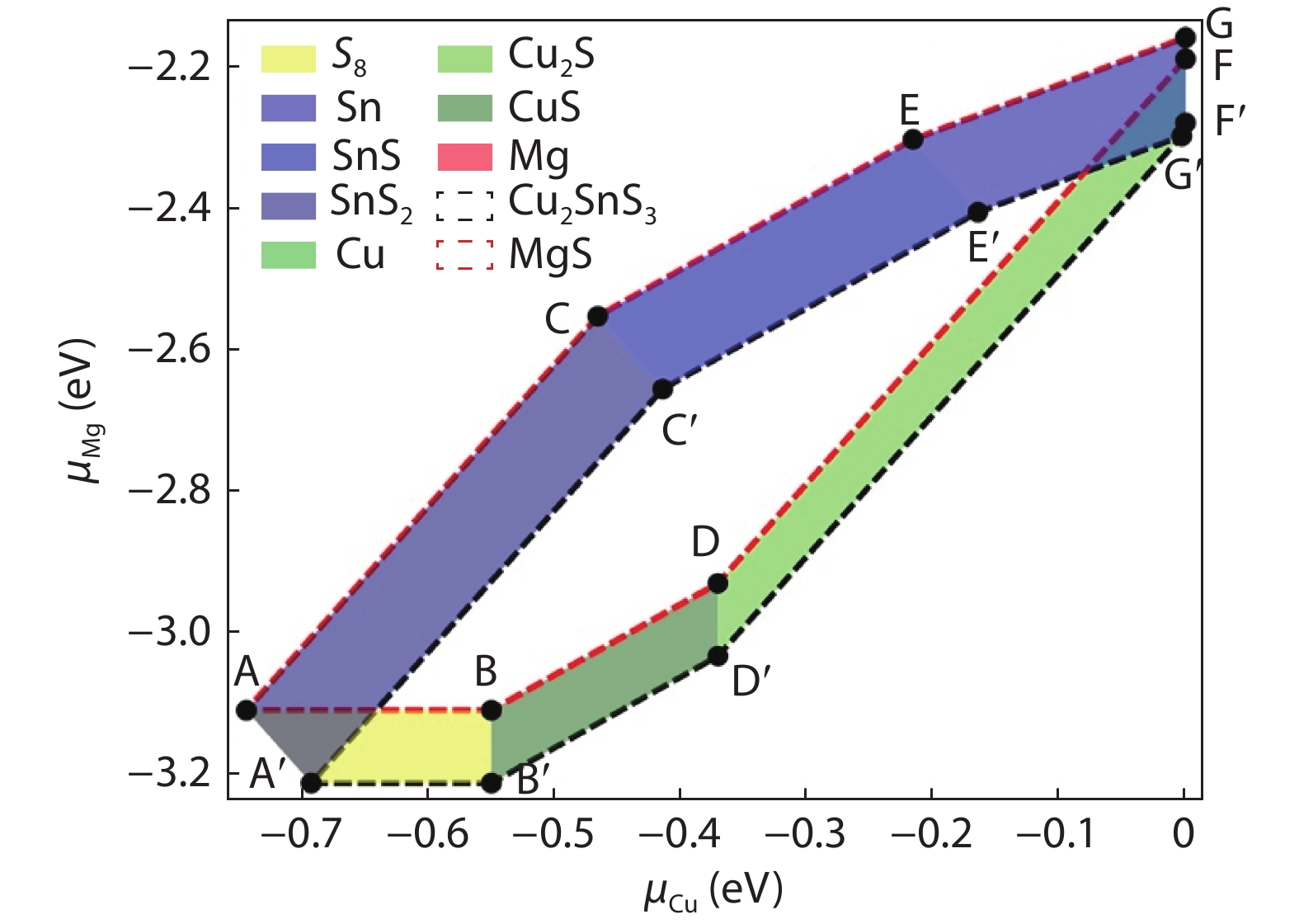
Fig. 1.  (Color online) Phase diagram of CMTS calculated from hybrid functional (HSE06).

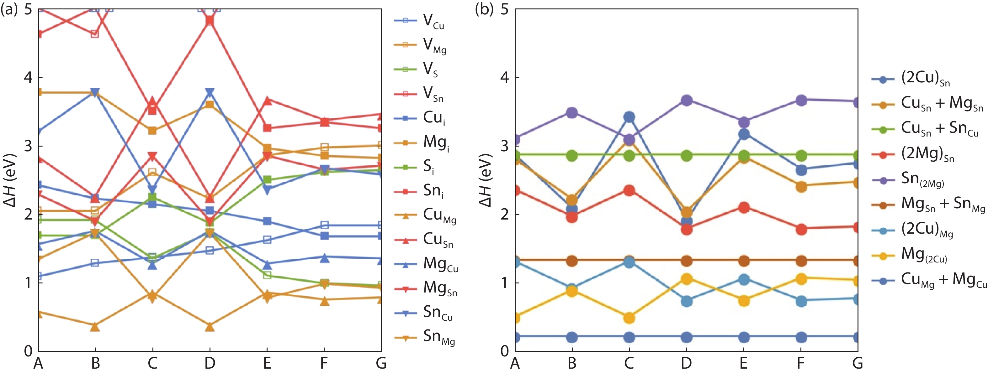
Fig. 2.  (Color online) Neutral defect formation energy for (a) intrinsic defects and (b) defect complexes in CMTS at chemical potentials ranging from Cu poorest (A) to Cu richest (G).

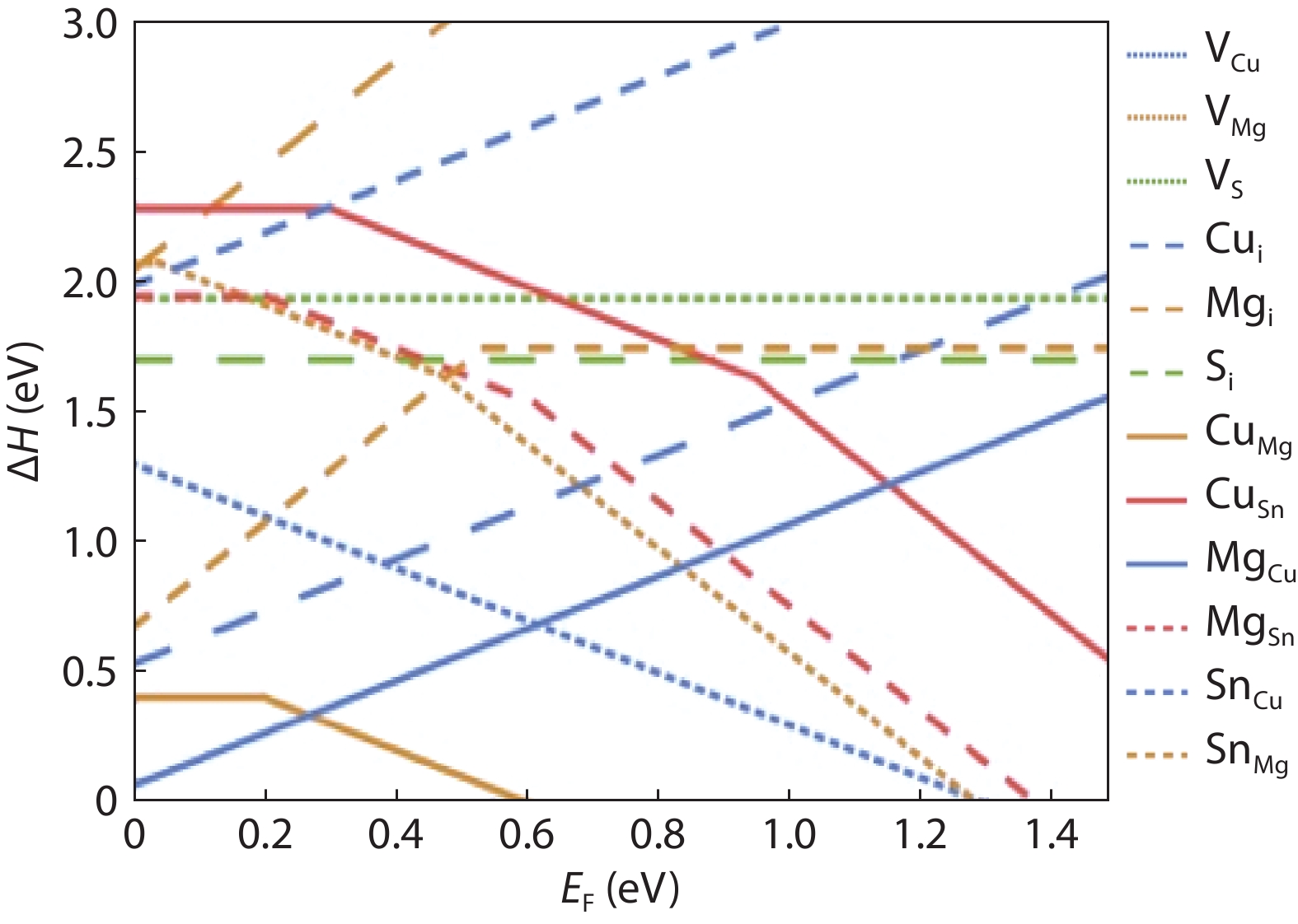
Fig. 3.  (Color online) Charged defect formation energy of point defects at chemical potential B, Fermi energy is varied from VBM to CBM.

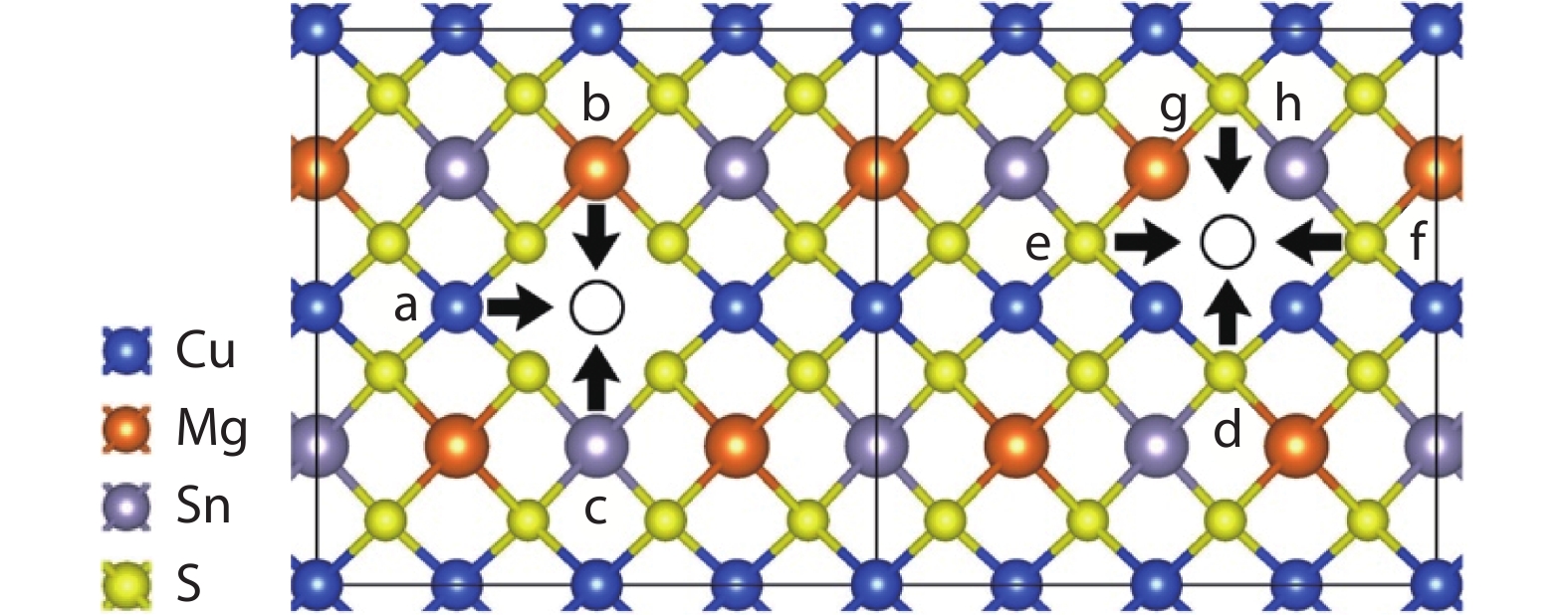
Fig. 4.  (Color online) Illustration of vacancy diffusion paths investigated in the current study.

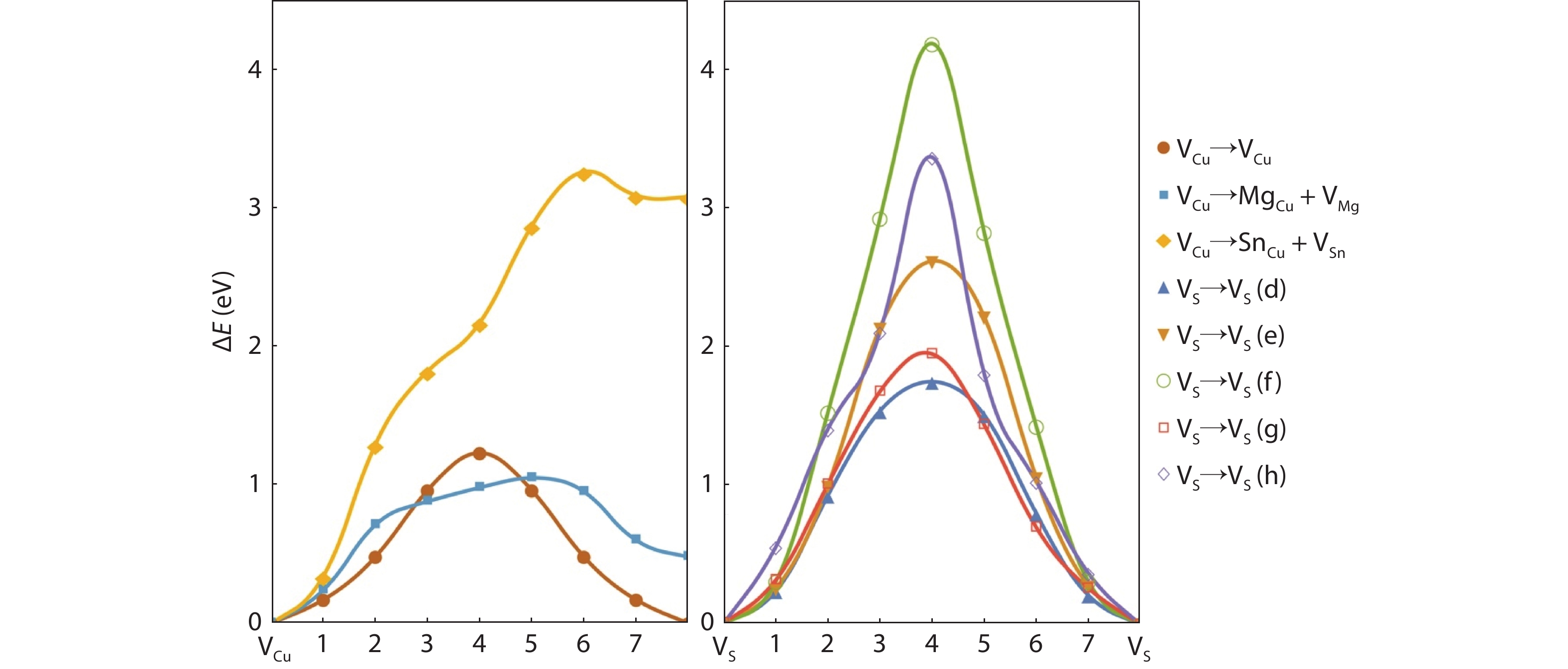
Fig. 5.  (Color online) Energy relative to VCu for cation and VS for anion diffusion along the MEP, energies of calculated images are represented by markers and solid lines are interpolation.

Table 1.   Listing of absolute formation energy of defect complexes (meV) at chemical potential point B along with separated point defects; binding energy is independent of chemical potential.

ParameterCuMg+MgCu(2Cu)MgMg(2Cu)MgSn+SnMg(CuMg)Sn(CuMg)Sn(2Cu)Sn
$ \Delta {H}_{\alpha } $CuMg0.44CuMg0.44VCu1.29MgSn1.89Mgi3.75MgSn1.89CuSn2.28
$ \Delta {H}_{\beta } $MgCu1.73Cui2.25MgCu1.73SnMg1.77CuSn2.28Cui2.25Cui2.25
$ \Delta {H}_{\alpha \beta } $0.240.880.871.352.422.422.12
$ {E}_{\mathrm{b}\mathrm{i}\mathrm{n}\mathrm{d}} $–1.93–1.81–2.15–2.31–3.61–1.72–2.41
DownLoad: CSV

Table 2.   Valence and conduction band edge shifts induced by low-energy fully compensated defect complexes in CMTS.

ParameterΔH at B (eV)ΔVBM (meV)ΔCBM (meV)ΔEg (meV)
CuMg+MgCu0.24+111+12–99
(2Cu)Mg0.88+15–13–28
Mg(2Cu)0.87–46+57103
MgSn+SnMg1.35+125-325–450
(2Mg)Sn1.95+86+72–14
DownLoad: CSV
[1]
Chen S Y, Gong X G, Walsh A, et al. Crystal and electronic band structure of Cu2ZnSnX4 (X = S and Se) photovoltaic absorbers: First-principles insights. Appl Phys Lett, 2009, 94, 041903 doi: 10.1063/1.3074499
[2]
He J, Sun L, Chen S Y, et al. Composition dependence of structure and optical properties of Cu2ZnSn(S, Se)4 solid solutions: An experimental study. J Alloys Compd, 2012, 511, 129 doi: 10.1016/j.jallcom.2011.08.099
[3]
Levcenco S, Dumcenco D, Wang Y P, et al. Influence of anionic substitution on the electrolyte electroreflectance study of band edge transitions in single crystal Cu2ZnSn(S xSe1− x)4 solid solutions. Opt Mater, 2012, 34, 1362 doi: 10.1016/j.optmat.2012.02.028
[4]
Persson C. Electronic and optical properties of Cu2ZnSnS4 and Cu2ZnSnSe4. J Appl Phys, 2010, 107, 053710 doi: 10.1063/1.3318468
[5]
Wang W, Winkler M T, Gunawan O, et al. Device characteristics of CZTSSe thin-film solar cells with 12.6% efficiency. Adv Energy Mater, 2014, 4, 1301465 doi: 10.1002/aenm.201301465
[6]
Yan C, Huang J L, Sun K W, et al. Cu2ZnSnS4 solar cells with over 10% power conversion efficiency enabled by heterojunction heat treatment. Nat Energy, 2018, 3, 764 doi: 10.1038/s41560-018-0206-0
[7]
Liu X L, Feng Y, Cui H T, et al. The current status and future prospects of kesterite solar cells: A brief review. Prog Photovolt: Res Appl, 2016, 24, 879 doi: 10.1002/pip.2741
[8]
Bishop D M, McCandless B, Gershon T, et al. Modification of defects and potential fluctuations in slow-cooled and quenched Cu2ZnSnSe4 single crystals. J Appl Phys, 2017, 121, 065704 doi: 10.1063/1.4975483
[9]
Zhuk S, Kushwaha A, Wong T K S, et al. Critical review on sputter-deposited Cu2ZnSnS4 (CZTS) based thin film photovoltaic technology focusing on device architecture and absorber quality on the solar cells performance. Sol Energy Mater Sol Cells, 2017, 171, 239 doi: 10.1016/j.solmat.2017.05.064
[10]
Gunawan O, Todorov T K, Mitzi D B. Loss mechanisms in hydrazine-processed Cu2ZnSn(Se, S)4 solar cells. Appl Phys Lett, 2010, 97, 233506 doi: 10.1063/1.3522884
[11]
Han D, Sun Y Y, Bang J, et al. Deep electron traps and origin of p-type conductivity in the earth-abundant solar-cell material Cu2ZnSnS4. Phys Rev B, 2013, 87, 155206 doi: 10.1103/PhysRevB.87.155206
[12]
Chen S Y, Walsh A, Gong X G, et al. Classification of lattice defects in the kesterite Cu2ZnSnS4 and Cu2ZnSnSe4 earth-abundant solar cell absorbers. Adv Mater, 2013, 25, 1522 doi: 10.1002/adma.201203146
[13]
Gokmen T, Gunawan O, Todorov T K, et al. Band tailing and efficiency limitation in kesterite solar cells. Appl Phys Lett, 2013, 103, 103506 doi: 10.1063/1.4820250
[14]
Romero M J, Du H, Teeter G, et al. Comparative study of the luminescence and intrinsic point defects in the kesterite Cu2ZnSnS4 and chalcopyrite Cu(In, Ga)Se2 thin films used in photovoltaic applications. Phys Rev B, 2011, 84, 165324 doi: 10.1103/PhysRevB.84.165324
[15]
Rey G, Larramona G, Bourdais S, et al. On the origin of band-tails in kesterite. Sol Energy Mater Sol Cells, 2018, 179, 142 doi: 10.1016/j.solmat.2017.11.005
[16]
Li J J, Wang D X, Li X L, et al. Cation substitution in earth-abundant kesterite photovoltaic materials. Adv Sci, 2018, 5, 1700744 doi: 10.1002/advs.201700744
[17]
Pal K, Singh P, Bhaduri A, et al. Current challenges and future prospects for a highly efficient (>20%) kesterite CZTS solar cell: A review. Sol Energy Mater Sol Cells, 2019, 196, 138 doi: 10.1016/j.solmat.2019.03.001
[18]
Kanevce A, Repins I, Wei S H. Impact of bulk properties and local secondary phases on the Cu2(Zn, Sn)Se4 solar cells open-circuit voltage. Sol Energy Mater Sol Cells, 2015, 133, 119 doi: 10.1016/j.solmat.2014.10.042
[19]
Kosyak V, Postnikov A V, Scragg J, et al. Calculation of point defect concentration in Cu2ZnSnS4: Insights into the high-temperature equilibrium and quenching. J Appl Phys, 2017, 122, 035707 doi: 10.1063/1.4994689
[20]
Huang D, Persson C. Band gap change induced by defect complexes in Cu2ZnSnS4. Thin Solid Films, 2013, 535, 265 doi: 10.1016/j.tsf.2012.10.030
[21]
Zawadzki P, Zakutayev A, Lany S. Entropy-driven clustering in tetrahedrally bonded multinary materials. Phys Rev Appl, 2015, 3, 034007 doi: 10.1103/PhysRevApplied.3.034007
[22]
Scragg J J S, Choubrac L, Lafond A, et al. A low-temperature order-disorder transition in Cu2ZnSnS4 thin films. Appl Phys Lett, 2014, 104, 041911 doi: 10.1063/1.4863685
[23]
Mendis B G, Goodman M C J, Major J D, et al. The role of secondary phase precipitation on grain boundary electrical activity in Cu2ZnSnS4 (CZTS) photovoltaic absorber layer material. J Appl Phys, 2012, 112, 124508 doi: 10.1063/1.4769738
[24]
Yang W C, Miskin C K, Carter N J, et al. Compositional inhomogeneity of multinary semiconductor nanoparticles: A case study of Cu2ZnSnS4. Chem Mater, 2014, 26, 6955 doi: 10.1021/cm502930d
[25]
Scragg J J, Wätjen J T, Edoff M, et al. A detrimental reaction at the molybdenum back contact in Cu2ZnSn(S, Se)4 thin-film solar cells. J Am Chem Soc, 2012, 134, 19330 doi: 10.1021/ja308862n
[26]
Scragg J J, Kubart T, Wätjen J T, et al. Effects of back contact instability on Cu2ZnSnS4 devices and processes. Chem Mater, 2013, 25, 3162 doi: 10.1021/cm4015223
[27]
Dalapati G K, Zhuk S, Masudy-Panah S, et al. Impact of molybdenum out diffusion and interface quality on the performance of sputter grown CZTS based solar cells. Sci Rep, 2017, 7, 1350 doi: 10.1038/s41598-017-01605-7
[28]
Bär M, Schubert B A, Marsen B, et al. Cliff-like conduction band offset and KCN-induced recombination barrier enhancement at the CdS/Cu2ZnSnS4 thin-film solar cell heterojunction. Appl Phys Lett, 2011, 99, 222105 doi: 10.1063/1.3663327
[29]
Nagaoka A, Miyake H, Taniyama T, et al. Effects of sodium on electrical properties in Cu2ZnSnS4 single crystal. Appl Phys Lett, 2014, 104, 152101 doi: 10.1063/1.4871208
[30]
Gershon T, Shin B, Bojarczuk N, et al. The role of sodium as a surfactant and suppressor of non-radiative recombination at internal surfaces in Cu2ZnSnS4. Adv Energy Mater, 2015, 5, 1400849 doi: 10.1002/aenm.201400849
[31]
Zhang Y O, Tse K, Xiao X D, et al. Controlling defects and secondary phases of CZTS by surfactant potassium. Phys Rev Mater, 2017, 1, 045403 doi: 10.1103/PhysRevMaterials.1.045403
[32]
Yan C, Liu F Y, Song N, et al. Band alignments of different buffer layers (CdS, Zn(O, S), and In2S3) on Cu2ZnSnS4. Appl Phys Lett, 2014, 104, 173901 doi: 10.1063/1.4873715
[33]
Sun K W, Yan C, Liu F Y, et al. Over 9% efficient kesterite Cu2ZnSnS4 solar cell fabricated by using Zn1– xCd xS buffer layer. Adv Energy Mater, 2016, 6, 1600046 doi: 10.1002/aenm.201600046
[34]
Li X L, Su Z H, Venkataraj S, et al. 8.6% Efficiency CZTSSe solar cell with atomic layer deposited Zn-Sn-O buffer layer. Sol Energy Mater Sol Cells, 2016, 157, 101 doi: 10.1016/j.solmat.2016.05.032
[35]
Li J J, Liu X R, Liu W, et al. Restraining the band fluctuation of CBD-Zn(O, S) layer: Modifying the hetero-junction interface for high performance Cu2ZnSnSe4 solar cells with Cd-free buffer layer. Sol RRL, 2017, 1, 1700075 doi: 10.1002/solr.201700075
[36]
Cui H T, Liu X L, Liu F Y, et al. Boosting Cu2ZnSnS4 solar cells efficiency by a thin Ag intermediate layer between absorber and back contact. Appl Phys Lett, 2014, 104, 041115 doi: 10.1063/1.4863951
[37]
Liu F Y, Sun K W, Li W, et al. Enhancing the Cu2ZnSnS4 solar cell efficiency by back contact modification: Inserting a thin TiB2 intermediate layer at Cu2ZnSnS4/Mo interface. Appl Phys Lett, 2014, 104, 051105 doi: 10.1063/1.4863736
[38]
Liu X L, Cui H T, Li W, et al. Improving Cu2ZnSnS4 (CZTS) solar cell performance by an ultrathin ZnO intermediate layer between CZTS absorber and Mo back contact. Phys Status Solidi RRL, 2014, 8, 966 doi: 10.1002/pssr.201409052
[39]
Tong Z F, Zhang K, Sun K W, et al. Modification of absorber quality and Mo-back contact by a thin Bi intermediate layer for kesterite Cu2ZnSnS4 solar cells. Sol Energy Mater Sol Cells, 2016, 144, 537 doi: 10.1016/j.solmat.2015.09.066
[40]
Gu Y C, Shen H P, Ye C, et al. All-solution-processed Cu2ZnSnS4 solar cells with self-depleted Na2S back contact modification layer. Adv Funct Mater, 2018, 28, 1703369 doi: 10.1002/adfm.201703369
[41]
Wang C C, Chen S Y, Yang J H, et al. Design of I2–II–IV–VI4 semiconductors through element substitution: The thermodynamic stability limit and chemical trend. Chem Mater, 2014, 26, 3411 doi: 10.1021/cm500598x
[42]
Zhong G H, Tse K, Zhang Y O, et al. Induced effects by the substitution of Zn in Cu2ZnSnX4 (X = S and Se). Thin Solid Films, 2016, 603, 224 doi: 10.1016/j.tsf.2016.02.005
[43]
Yuan Z K, Chen S Y, Xiang H J, et al. Engineering solar cell absorbers by exploring the band alignment and defect disparity: The case of Cu- and Ag-based kesterite compounds. Adv Funct Mater, 2015, 25, 6733 doi: 10.1002/adfm.201502272
[44]
Qi Y F, Kou D X, Zhou W H, et al. Engineering of interface band bending and defects elimination via a Ag-graded active layer for efficient (Cu, Ag)2ZnSn(S, Se)4 solar cells. Energy Environ Sci, 2017, 10, 2401 doi: 10.1039/C7EE01405H
[45]
Su Z H, Tan J M R, Li X L, et al. Cation substitution of solution-processed Cu2ZnSnS4 thin film solar cell with over 9% efficiency. Adv Energy Mater, 2015, 5, 1500682 doi: 10.1002/aenm.201500682
[46]
Bag S, Gunawan O, Gokmen T, et al. Hydrazine-processed Ge-substituted CZTSe solar cells. Chem Mater, 2012, 24, 4588 doi: 10.1021/cm302881g
[47]
Collord A D, Hillhouse H W. Germanium alloyed kesterite solar cells with low voltage deficits. Chem Mater, 2016, 28, 2067 doi: 10.1021/acs.chemmater.5b04806
[48]
Wei M, Du Q Y, Wang R, et al. Synthesis of new earth-abundant kesterite Cu2MgSnS4 nanoparticles by hot-injection method. Chem Lett, 2014, 43, 1149 doi: 10.1246/cl.140208
[49]
Agawane G L, Vanalakar S A, Kamble A S, et al. Fabrication of Cu2(Zn xMg1– x)SnS4 thin films by pulsed laser deposition technique for solar cell applications. Mater Sci Semicond Process, 2018, 76, 50 doi: 10.1016/j.mssp.2017.12.010
[50]
Yang G, Zhai X L, Li Y F, et al. Synthesis and characterizations of Cu2MgSnS4 thin films with different sulfuration temperatures. Mater Lett, 2019, 242, 58 doi: 10.1016/j.matlet.2019.01.102
[51]
Caballero R, Haass S G, Andres C, et al. Effect of magnesium incorporation on solution-processed kesterite solar cells. Front Chem, 2018, 6, 5 doi: 10.3389/fchem.2018.00005
[52]
Lie S, Leow S W, Bishop D M, et al. Improving carrier-transport properties of CZTS by Mg incorporation with spray pyrolysis. ACS Appl Mater Interfaces, 2019, 11, 25824 doi: 10.1021/acsami.9b05244
[53]
Chen S Y, Yang J H, Gong X G, et al. Intrinsic point defects and complexes in the quaternary kesterite semiconductor Cu2ZnSnS4. Phys Rev B, 2010, 81, 245204 doi: 10.1103/PhysRevB.81.245204
[54]
Hinuma Y, Grüneis A, Kresse G, et al. Band alignment of semiconductors from density-functional theory and many-body perturbation theory. Phys Rev B, 2014, 90, 155405 doi: 10.1103/PhysRevB.90.155405
[55]
Wei S H. Overcoming the doping bottleneck in semiconductors. Comput Mater Sci, 2004, 30, 337 doi: 10.1016/j.commatsci.2004.02.024
[56]
Freysoldt C, Neugebauer J, van de Walle C G. Fully ab initio finite-size corrections for charged-defect supercell calculations. Phys Rev Lett, 2009, 102, 016402 doi: 10.1103/PhysRevLett.102.016402
[57]
Chen S Y, Gong X G, Walsh A, et al. Electronic structure and stability of quaternary chalcogenide semiconductors derived from cation cross-substitution of II-VI and I-III-VI2 compounds. Phys Rev B, 2009, 79, 165211 doi: 10.1103/PhysRevB.79.165211
[58]
Zhu J Y, Liu F, Stringfellow G B, et al. Strain-enhanced doping in semiconductors: Effects of dopant size and charge state. Phys Rev Lett, 2010, 105, 195503 doi: 10.1103/PhysRevLett.105.195503
[59]
Hu H, Liu M, Wang Z F, et al. Quantum electronic stress: Density-functional-theory formulation and physical manifestation. Phys Rev Lett, 2012, 109, 055501 doi: 10.1103/PhysRevLett.109.055501
[60]
Noufi R, Axton R, Herrington C, et al. Electronic properties versus composition of thin films of CuInSe2. Appl Phys Lett, 1984, 45, 668 doi: 10.1063/1.95350
[61]
Xiao W, Wang J N, Zhao X S, et al. Intrinsic defects and Na doping in Cu2ZnSnS4: A density-functional theory study. Sol Energy, 2015, 116, 125 doi: 10.1016/j.solener.2015.04.005
[62]
Henkelman G, Uberuaga B P, Jónsson H. A climbing image nudged elastic band method for finding saddle points and minimum energy paths. J Chem Phys, 2000, 113, 9901 doi: 10.1063/1.1329672
[63]
Perdew J P, Burke K, Ernzerhof M. Generalized gradient approximation made simple. Phys Rev Lett, 1996, 77, 3865 doi: 10.1103/PhysRevLett.77.3865
[64]
Nakamura S, Maeda T, Wada T. First-principles study of diffusion of Cu and in atoms in CuInSe2. Jpn J Appl Phys, 2013, 52, 04CR01 doi: 10.7567/JJAP.52.04CR01
  • Search

    Advanced Search >>

    GET CITATION

    shu

    Export: BibTex EndNote

    Article Metrics

    Article views: 2636 Times PDF downloads: 109 Times Cited by: 0 Times

    History

    Received: 08 July 2021 Revised: 29 July 2021 Online: Accepted Manuscript: 21 October 2021Uncorrected proof: 17 November 2021Published: 01 February 2022

    Catalog

      Email This Article

      User name:
      Email:*请输入正确邮箱
      Code:*验证码错误
      Kin Fai Tse, Shengyuan Wang, Man Hoi Wong, Junyi Zhu. Defects properties and vacancy diffusion in Cu2MgSnS4 [J]. Journal of Semiconductors, 2022, 43(2): 022101. doi: 10.1088/1674-4926/43/2/022101 ****K F Tse, S Y Wang, M H Wong, J Y Zhu, Defects properties and vacancy diffusion in Cu2MgSnS4[J]. J. Semicond., 2022, 43(2): 022101. doi: 10.1088/1674-4926/43/2/022101.
      Citation:
      Kin Fai Tse, Shengyuan Wang, Man Hoi Wong, Junyi Zhu. Defects properties and vacancy diffusion in Cu2MgSnS4 [J]. Journal of Semiconductors, 2022, 43(2): 022101. doi: 10.1088/1674-4926/43/2/022101 ****
      K F Tse, S Y Wang, M H Wong, J Y Zhu, Defects properties and vacancy diffusion in Cu2MgSnS4[J]. J. Semicond., 2022, 43(2): 022101. doi: 10.1088/1674-4926/43/2/022101.

      Defects properties and vacancy diffusion in Cu2MgSnS4

      DOI: 10.1088/1674-4926/43/2/022101
      More Information
      • Kin Fai Tse:has obtained his Ph.D. and Bsc degrees in Physics at The Chinese University of Hong Kong in 2020and 2015, respectively. His research interest is focus on defects in photovoltaic materials
      • Shengyuan Wang:is currently a Ph.D. student in Department of Physics at The Chinese University of Hong Kong.He has obtained his Bachelor's degree in Physics at Shanghai Jiao Tong University in 2020. His research interest is focus on defect and surface calculations in the area of semiconductor physics
      • Junyi Zhu:is an associate professor at the Department of Physics, The Chinese University of Hong Kong. He received his B.S. degree from Peking University in 1998. He received his Ph.D. degree from University of Utah in 2009. His research interests mainly include semiconductor defects and doping, electronic properties of solids, surface and interface phenomena, using first-principles and molecular dynamics approaches and elastic theory modeling
      • Corresponding author: jyzhu@phy.cuhk.edu.hk
      • Received Date: 2021-07-08
      • Revised Date: 2021-07-29
      • Published Date: 2022-02-10

      Catalog

        /

        DownLoad:  Full-Size Img  PowerPoint
        Return
        Return