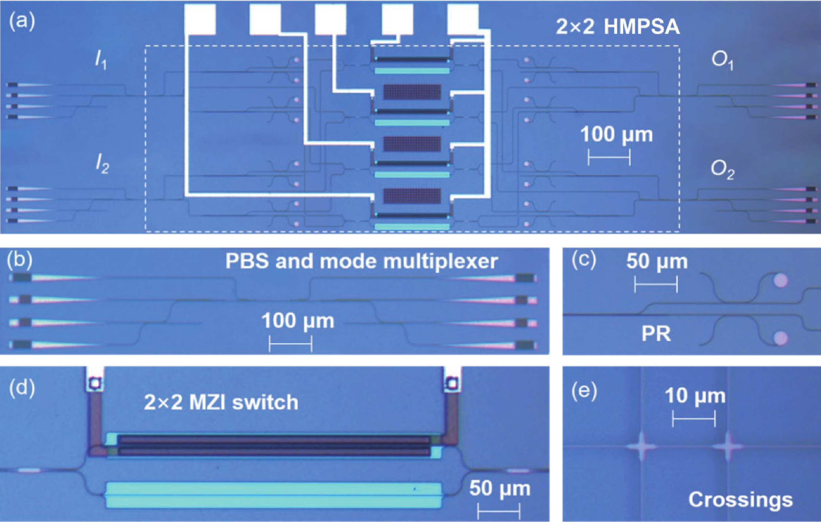
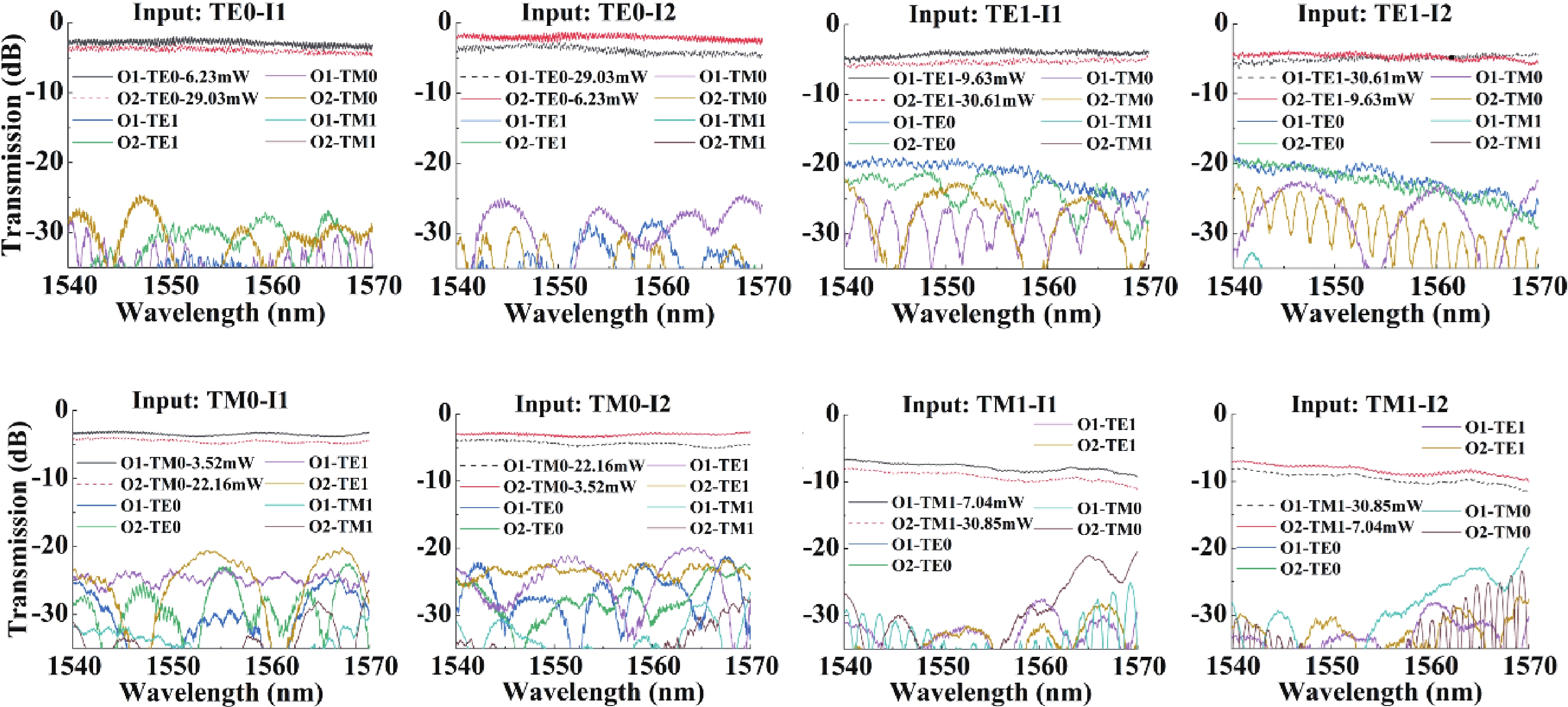
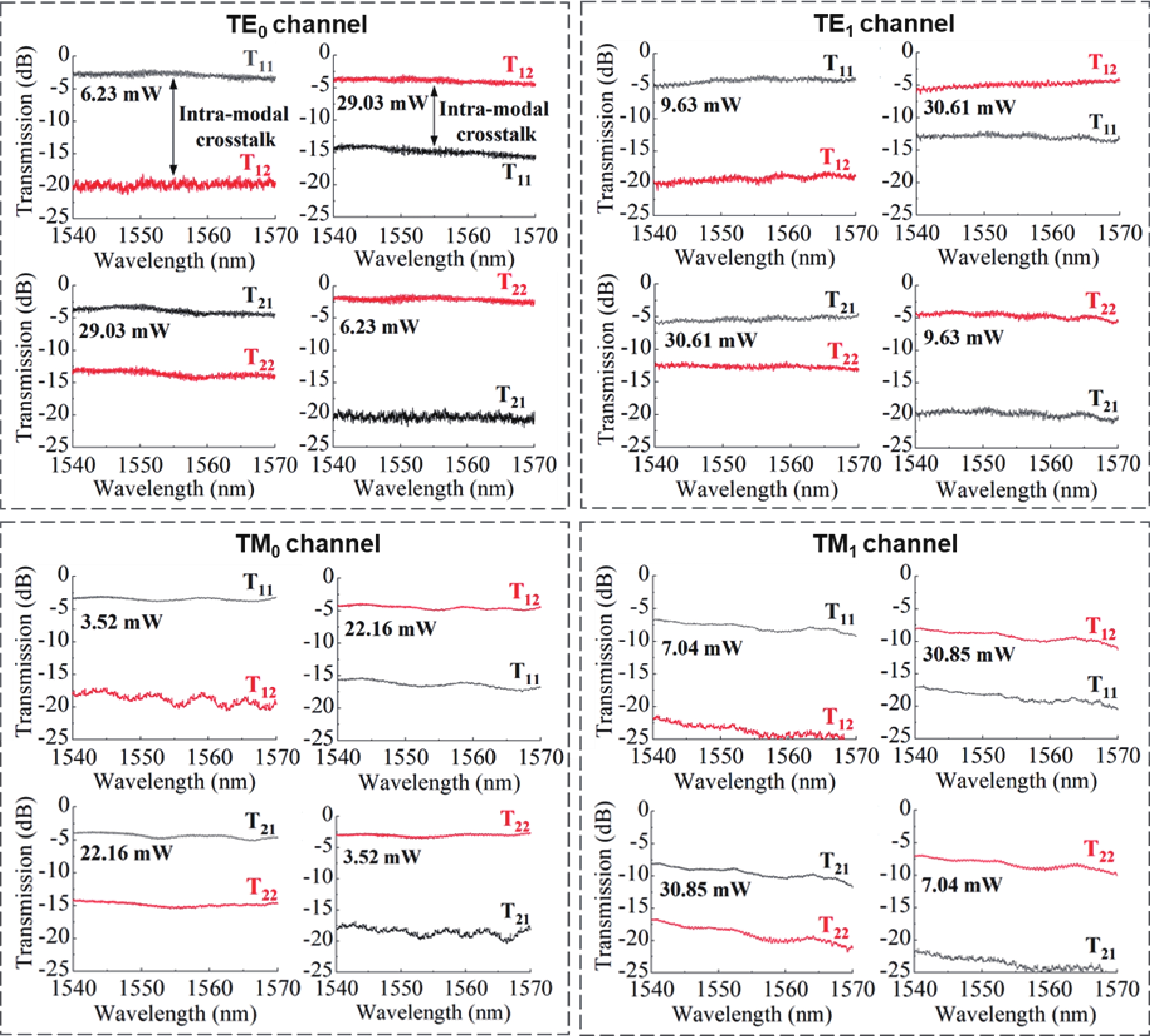
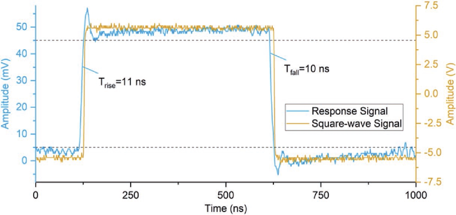
| [1] |
Winzer P J, Neilson D T, Chraplyvy A R. Fiber-optic transmission and networking: The previous 20 and the next 20 years. Opt Express, 2018, 26, 24190 doi: 10.1364/OE.26.024190 |
| [2] |
Stern B, Zhu X L, Chen C P, et al. On-chip mode-division multiplexing switch. Optica, 2015, 2, 530 doi: 10.1364/OPTICA.2.000530 |
| [3] |
Xiong Y L, Priti R B, Liboiron-Ladouceur O. High-speed two-mode switch for mode-division multiplexing optical networks. Optica, 2017, 4, 1098 doi: 10.1364/OPTICA.4.001098 |
| [4] |
Yao Y H, Cheng Z, Dong J J, et al. Performance of integrated optical switches based on 2D materials and beyond. Front Optoelectron, 2020, 13, 129 doi: 10.1007/s12200-020-1058-3 |
| [5] |
Zhao Y H, Wang X, Gao D S, et al. On-chip programmable pulse processor employing cascaded MZI-MRR structure. Front Optoelectron, 2019, 12, 148 doi: 10.1007/s12200-018-0846-5 |
| [6] |
Su Y K, Zhang Y, Qiu C Y, et al. Silicon photonic platform for passive waveguide devices: Materials, fabrication, and applications. Adv Mater Technol, 2020, 5, 1901153 doi: 10.1002/admt.201901153 |
| [7] |
Luo L W, Ophir N, Chen C P, et al. WDM-compatible mode-division multiplexing on a silicon chip. Nat Commun, 2014, 5, 3069 doi: 10.1038/ncomms4069 |
| [8] |
Jia H, Yang S L, Zhou T, et al. WDM-compatible multimode optical switching system-on-chip. Nanophotonics, 2019, 8, 889 doi: 10.1515/nanoph-2019-0005 |
| [9] |
Han L S, Kuo B P P, Alic N, et al. Silicon Photonic Wavelength and Mode Selective Switch for WDM-MDM networks. 2019 Optical Fiber Communication Conference (OFC), 2019, 1
|
| [10] |
Jia H, Zhou T, Zhang L, et al. Optical switch compatible with wavelength division multiplexing and mode division multiplexing for photonic networks-on-chip. Opt Express, 2017, 25, 20698 doi: 10.1364/OE.25.020698 |
| [11] |
Zhang Y, He Y, Zhu Q M, et al. On-chip silicon photonic 2 × 2 mode- and polarization-selective switch with low inter-modal crosstalk. Photon Res, 2017, 5, 521 doi: 10.1364/PRJ.5.000521 |
| [12] |
Zhang Y, Zhang R H, Zhu Q M, et al. Architecture and devices for silicon photonic switching in wavelength, polarization and mode. J Light Technol, 2019, 38, 215 doi: 10.1109/JLT.2019.2946171 |
| [13] |
Dai D, Wang J, Shi Y. Silicon mode (de)multiplexer enabling high capacity photonic networks-on-chip with a single-wavelength-carrier light. Opt Lett, 2013, 38, 1422 doi: 10.1364/OL.38.001422 |
| [14] |
Liu Y Y, Shainline J M, Zeng X G, et al. Ultra-low-loss CMOS-compatible waveguide crossing arrays based on multimode Bloch waves and imaginary coupling. Opt Lett, 2014, 39, 335 doi: 10.1364/OL.39.000335 |
| [15] |
Siew S Y, Li B, Gao F, et al. Review of silicon photonics technology and platform development. J Light Technol, 2021, 39, 4374 doi: 10.1109/JLT.2021.3066203 |
| [16] |
Driscoll J B, Grote R R, Souhan B, et al. Asymmetric Y junctions in silicon waveguides for on-chip mode-division multiplexing. Opt Lett, 2013, 38, 1854 doi: 10.1364/OL.38.001854 |
| [17] |
Chen W, Wang P, Yang J. Mode multi/demultiplexer based on cascaded asymmetric Y-junctions. Opt Express, 2013, 21, 25113 doi: 10.1364/OE.21.025113 |
| [18] |
Uematsu T, Ishizaka Y, Kawaguchi Y, et al. Design of a compact two-mode multi/demultiplexer consisting of multimode interference waveguides and a wavelength-insensitive phase shifter for mode-division multiplexing transmission. J Light Technol, 2012, 30, 2421 doi: 10.1109/JLT.2012.2199961 |
| [19] |
Sun Y, Xiong Y L, Ye W N. Experimental demonstration of a two-mode (de)multiplexer based on a taper-etched directional coupler. Opt Lett, 2016, 41, 3743 doi: 10.1364/OL.41.003743 |
| [20] |
Jia H, Zhang L, Ding J, et al. Microring modulator matrix integrated with mode multiplexer and de-multiplexer for on-chip optical interconnect. Opt Express, 2017, 25, 422 doi: 10.1364/OE.25.000422 |
| [21] |
Dai D, Mao M. Mode converter based on an inverse taper for multimode silicon nanophotonic integrated circuits. Opt Express, 2015, 23, 28376 doi: 10.1364/OE.23.028376 |
| [22] |
Jiang W F, Miao J Y, Li T. Compact silicon 10-mode multi/demultiplexer for hybrid mode- and polarisation-division multiplexing system. Sci Rep, 2019, 9, 13223 doi: 10.1038/s41598-019-49763-0 |
| [23] |
Zhang Y, He Y, Wang H W, et al. Ultra-broadband mode size converter using on-chip metamaterial-based Luneburg lens. ACS Photonics, 2021, 8, 202 doi: 10.1021/acsphotonics.0c01269 |
| [24] |
Zheng X, Chang E, Amberg P, et al. A high-speed, tunable silicon photonic ring modulator integrated with ultra-efficient active wavelength control. Opt Express, 2014, 22, 12628 doi: 10.1364/OE.22.012628 |
| [25] |
Jayatilleka H, Murray K, Guillén-Torres M Á, et al. Wavelength tuning and stabilization of microring-based filters using silicon in-resonator photoconductive heaters. Opt Express, 2015, 23, 25084 doi: 10.1364/OE.23.025084 |
| [26] |
Dai D X, Li C L, Wang S P, et al. 10-channel mode (de)multiplexer with dual polarizations. Laser Photonics Rev, 2018, 12, 1700109 doi: 10.1002/lpor.201700109 |
| [27] |
Xu D X, Schmid J H, Reed G T, et al. Silicon photonic integration platform — have we found the sweet spot. IEEE J Sel Top Quantum Electron, 2014, 20, 189 doi: 10.1109/JSTQE.2014.2299634 |
| [28] |
Huang H Z, Huang Y T, He Y, et al. Demonstration of terabit coherent on-chip optical interconnects employing mode-division multiplexing. Opt Lett, 2021, 46, 2292 doi: 10.1364/OL.424727 |
| [29] |
Okuno M, Kato K, Nagase R, et al. Silica-based 8 × 8 optical matrix switch integrating new switching units with large fabrication tolerance. J Light Technol, 1999, 17, 771 doi: 10.1109/50.762891 |
| [30] |
Suzuki K, Cong G, Tanizawa K, et al. Ultra-high-extinction-ratio 2 × 2 silicon optical switch with variable splitter. Opt Express, 2015, 23, 9086 doi: 10.1364/OE.23.009086 |
| [31] |
He Y, Zhang Y, Zhu Q M, et al. Silicon high-order mode (de)multiplexer on single polarization. J Light Technol, 2018, 36, 5746 doi: 10.1109/JLT.2018.2878529 |


 DownLoad: