ARTICLES

Instability of parasitic capacitance in T-shape-gate enhancement-mode AlGaN/GaN MIS-HEMTs

Lan Bi1, 2, Yixu Yao1, 2, Qimeng Jiang1, 2, , Sen Huang1, 2, , Xinhua Wang1, 2, Hao Jin1, 2, Xinyue Dai1, 2, Zhengyuan Xu1, Jie Fan1, 2, Haibo Yin1, 2, Ke Wei1, 2 and Xinyu Liu1, 2

+ Author Affiliations

 Corresponding author: Qimeng Jiang, jiangqimeng@ime.ac.cn; Sen Huang, huangsen@ime.ac.cn

PDF

Turn off MathJax

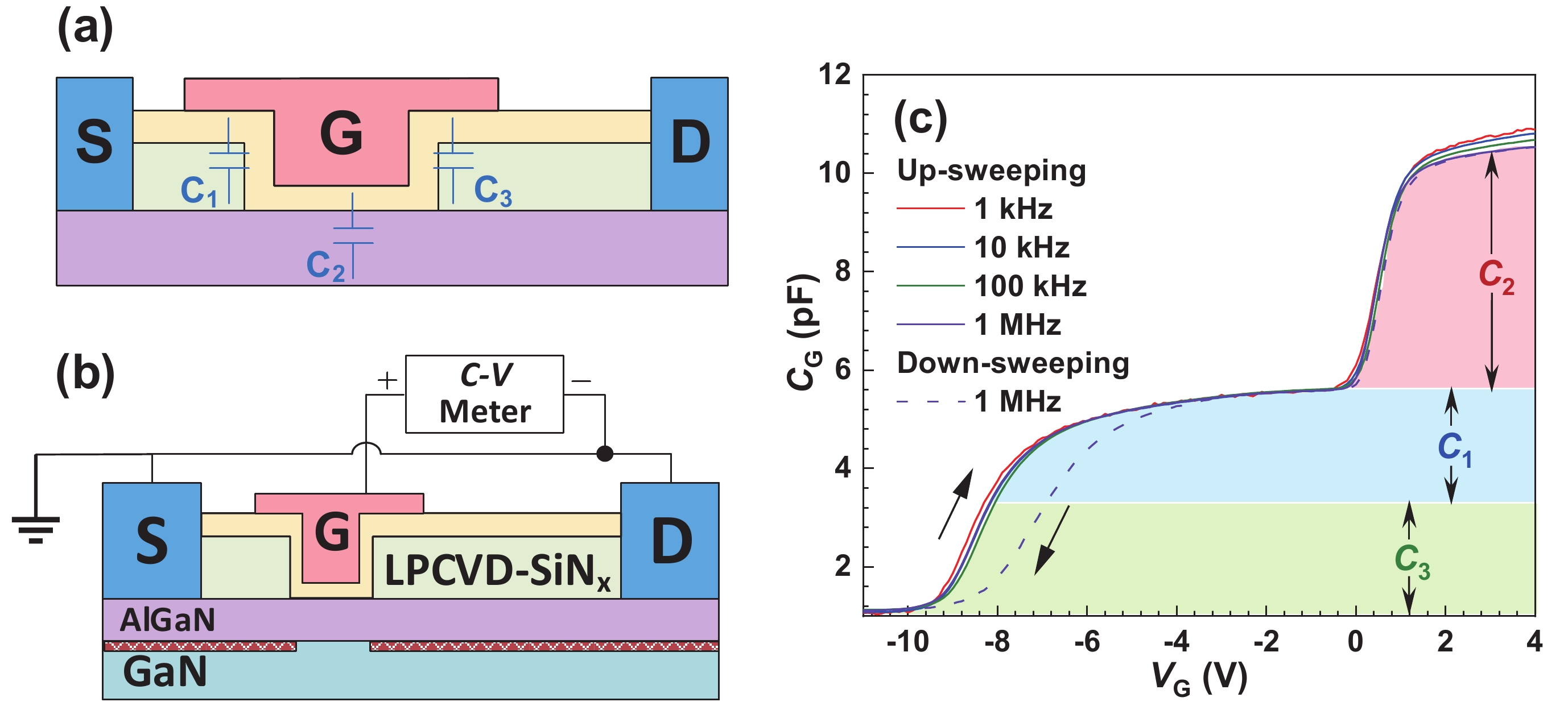
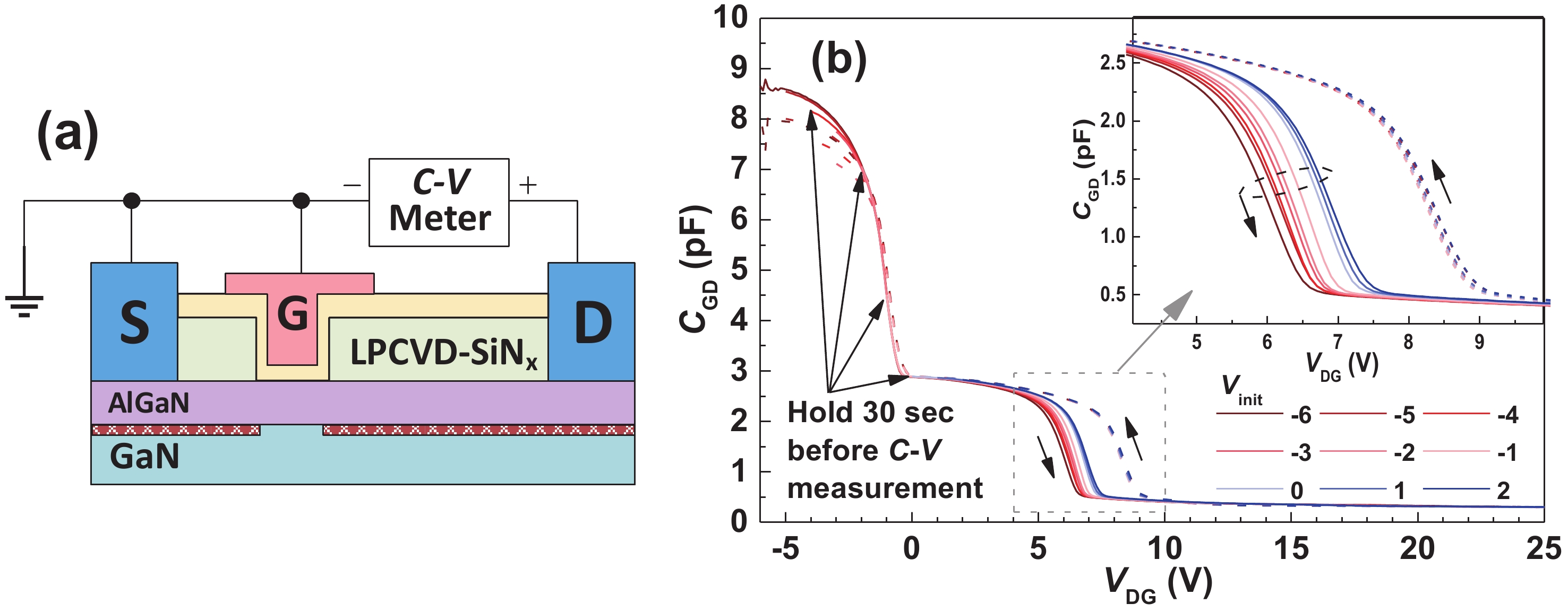
Abstract: Parasitic capacitances associated with overhangs of the T-shape-gate enhancement-mode (E-mode) GaN-based power device, were investigated by frequency/voltage-dependent capacitance–voltage and inductive-load switching measurements. The overhang capacitances induce a pinch-off voltage distinguished from that of the E-mode channel capacitance in the gate capacitance and the gate–drain capacitance characteristic curves. Frequency- and voltage-dependent tests confirm the instability caused by the trapping of interface/bulk states in the LPCVD-SiNx passivation dielectric. Circuit-level double pulse measurement also reveals its impact on switching transition for power switching applications.

Key words: AlGaN/GaN MIS-HEMTsenhancement-modeT-shape gateparasitic capacitancetrapping/de-trappingcapacitance-voltage hysteresis


[1]
Boutros K S, Chu R M, Hughes B. GaN power electronics for automotive application. 2012 IEEE Energytech, 2012, 1
[2]
Piedra D, Lu B, Sun M, et al. Advanced power electronic devices based on gallium nitride (GaN). 2015 IEEE International Electron Devices Meeting, 2015, 16.6.1
[3]
Kizilyalli I C, Xu Y A, Carlson E, et al. Current and future directions in power electronic devices and circuits based on wide band-gap semiconductors. 2017 IEEE 5th Work Wide Bandgap Power Devices Appl, 2017, 417
[4]
Chen K J, Häberlen O, Lidow A, et al. GaN-on-Si power technology: Devices and applications. IEEE Trans Electron Devices, 2017, 64, 779 doi: 10.1109/TED.2017.2657579
[5]
Saito W, Nitta T, Kakiuchi Y, et al. Suppression of dynamic on-resistance increase and gate charge measurements in high-voltage GaN-HEMTs with optimized field-plate structure. IEEE Trans Electron Devices, 2007, 54, 1825 doi: 10.1109/TED.2007.901150
[6]
Chu R M, Corrion A, Chen M, et al. 1200-V normally off GaN-on-Si field-effect transistors with low dynamic on -resistance. IEEE Electron Device Lett, 2011, 32, 632 doi: 10.1109/LED.2011.2118190
[7]
Ma X B, Zhang J C, Guo L L, et al. Effects of passivation and FP structure on current collapse in an AlGaN/GaN HEMT. Chin J Semicond, 2007, 28, 73
[8]
Lei Y, Lu H. Influence of field plate on surface-state-related lag characteristics of AlGaN/GaN HEMT. J Semicond, 2015, 36, 074007 doi: 10.1088/1674-4926/36/7/074007
[9]
Meneghesso G, Bisi D, Rossetto I, et al. Reliability of power devices: Bias-induced threshold voltage instability and dielectric breakdown in GaN MIS-HEMTs. 2016 IEEE Int Integr Reliab Work, 2016, 35
[10]
Zhao R, Huang S, Wang X H, et al. Interface charge engineering in down-scaled AlGaN (<6 nm)/GaN heterostructure for fabrication of GaN-based power HEMTs and MIS-HEMTs. Appl Phys Lett, 2020, 116, 103502 doi: 10.1063/1.5134886
[11]
Yang S, Tang Z K, Hua M Y, et al. Investigation of SiN x and AlN passivation for AlGaN/GaN high-electron-mobility transistors: Role of interface traps and polarization charges. IEEE J Electron Devices Soc, 2020, 8, 358 doi: 10.1109/JEDS.2020.2984016
[12]
Viey A G, Vandendaele W, Jaud M A, et al. Investigation of nBTI degradation on GaN-on-Si E-mode MOSc-HEMT. 2019 IEEE International Electron Devices Meeting, 2019, 4.3.1
[13]
Huang S, Liu X, Wang X, et al. Ultrathin-barrier AlGaN/GaN heterostructure: a recess-free technology for manufacturing high-performance GaN-on-Si power devices. IEEE Trans on Electron Devices, 2018, 65, 207 doi: 10.1109/TED.2017.2773201
[14]
Huang S, Wang X H, Liu X Y, et al. Monolithic integration of E/D-mode GaN MIS-HEMTs on ultrathin-barrier AlGaN/GaN heterostructure on Si substrates. Appl Phys Express, 2019, 12, 024001 doi: 10.7567/1882-0786/aafa0e
[15]
Huang S, Liu X Y, Wang X H, et al. High uniformity normally-OFF GaN MIS-HEMTs fabricated on ultra-thin-barrier AlGaN/GaN heterostructure. IEEE Electron Device Lett, 2016, 37, 1617 doi: 10.1109/LED.2016.2617381
[16]
Guo F Q, Huang S, Wang X H, et al. Suppression of interface states between nitride-based gate dielectrics and ultrathin-barrier AlGaN/GaN heterostructure with in situ remote plasma pretreatments. Appl Phys Lett, 2021, 118, 093503 doi: 10.1063/5.0041421
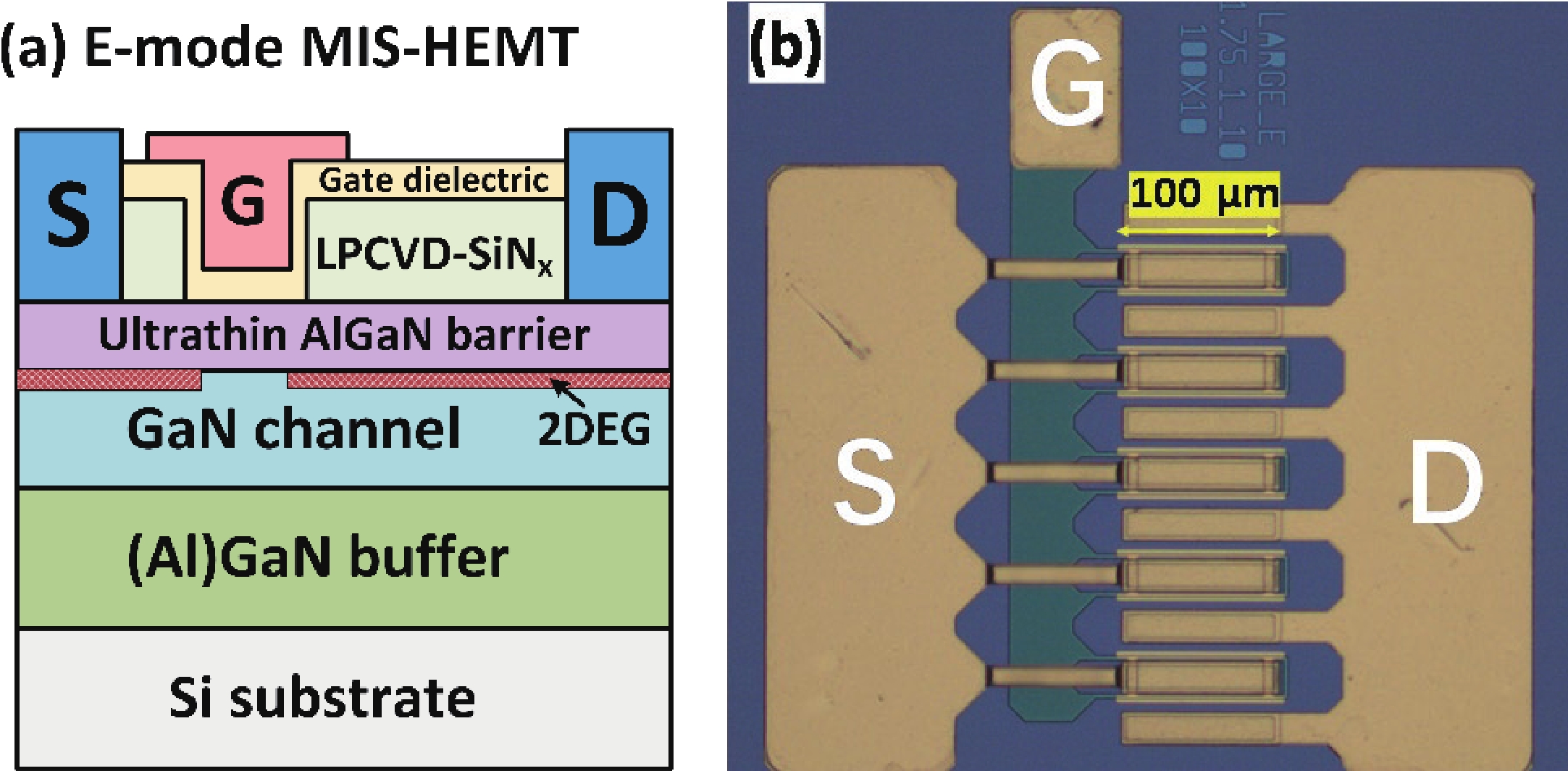
Fig. 1.  (Color online) (a) Cross sectional schematic of the E-mode AlGaN/GaN MIS-HEMT. (b) Microscope photograph of a 1-mm device.

Fig. 2.  (Color online) (a) Transfer, (b) output, and (c) three-terminal off-state leakage of the 1-mm E-mode MIS-HEMT.

Fig. 3.  (Color online) (a) Schematic of the gate-related capacitances in T-shape gate E-mode AlGaN/GaN MIS-HEMT. (b) Bias set of the CG–VG measurement, and (c) the multi-frequency curves of the 1-mm MIS-HEMT.

Fig. 4.  (Color online) (a) Bias set of the CGD measurement. (b) CGDVDG curves with varied hold and forward stressing voltage.

Fig. 5.  (Color online) (a) Schematic and photo of the inductive switching circuit. (b) Waveform of the inductive switching under 50-V VBUS and (c) the turn-on transients of the DUT.

[1]
Boutros K S, Chu R M, Hughes B. GaN power electronics for automotive application. 2012 IEEE Energytech, 2012, 1
[2]
Piedra D, Lu B, Sun M, et al. Advanced power electronic devices based on gallium nitride (GaN). 2015 IEEE International Electron Devices Meeting, 2015, 16.6.1
[3]
Kizilyalli I C, Xu Y A, Carlson E, et al. Current and future directions in power electronic devices and circuits based on wide band-gap semiconductors. 2017 IEEE 5th Work Wide Bandgap Power Devices Appl, 2017, 417
[4]
Chen K J, Häberlen O, Lidow A, et al. GaN-on-Si power technology: Devices and applications. IEEE Trans Electron Devices, 2017, 64, 779 doi: 10.1109/TED.2017.2657579
[5]
Saito W, Nitta T, Kakiuchi Y, et al. Suppression of dynamic on-resistance increase and gate charge measurements in high-voltage GaN-HEMTs with optimized field-plate structure. IEEE Trans Electron Devices, 2007, 54, 1825 doi: 10.1109/TED.2007.901150
[6]
Chu R M, Corrion A, Chen M, et al. 1200-V normally off GaN-on-Si field-effect transistors with low dynamic on -resistance. IEEE Electron Device Lett, 2011, 32, 632 doi: 10.1109/LED.2011.2118190
[7]
Ma X B, Zhang J C, Guo L L, et al. Effects of passivation and FP structure on current collapse in an AlGaN/GaN HEMT. Chin J Semicond, 2007, 28, 73
[8]
Lei Y, Lu H. Influence of field plate on surface-state-related lag characteristics of AlGaN/GaN HEMT. J Semicond, 2015, 36, 074007 doi: 10.1088/1674-4926/36/7/074007
[9]
Meneghesso G, Bisi D, Rossetto I, et al. Reliability of power devices: Bias-induced threshold voltage instability and dielectric breakdown in GaN MIS-HEMTs. 2016 IEEE Int Integr Reliab Work, 2016, 35
[10]
Zhao R, Huang S, Wang X H, et al. Interface charge engineering in down-scaled AlGaN (<6 nm)/GaN heterostructure for fabrication of GaN-based power HEMTs and MIS-HEMTs. Appl Phys Lett, 2020, 116, 103502 doi: 10.1063/1.5134886
[11]
Yang S, Tang Z K, Hua M Y, et al. Investigation of SiN x and AlN passivation for AlGaN/GaN high-electron-mobility transistors: Role of interface traps and polarization charges. IEEE J Electron Devices Soc, 2020, 8, 358 doi: 10.1109/JEDS.2020.2984016
[12]
Viey A G, Vandendaele W, Jaud M A, et al. Investigation of nBTI degradation on GaN-on-Si E-mode MOSc-HEMT. 2019 IEEE International Electron Devices Meeting, 2019, 4.3.1
[13]
Huang S, Liu X, Wang X, et al. Ultrathin-barrier AlGaN/GaN heterostructure: a recess-free technology for manufacturing high-performance GaN-on-Si power devices. IEEE Trans on Electron Devices, 2018, 65, 207 doi: 10.1109/TED.2017.2773201
[14]
Huang S, Wang X H, Liu X Y, et al. Monolithic integration of E/D-mode GaN MIS-HEMTs on ultrathin-barrier AlGaN/GaN heterostructure on Si substrates. Appl Phys Express, 2019, 12, 024001 doi: 10.7567/1882-0786/aafa0e
[15]
Huang S, Liu X Y, Wang X H, et al. High uniformity normally-OFF GaN MIS-HEMTs fabricated on ultra-thin-barrier AlGaN/GaN heterostructure. IEEE Electron Device Lett, 2016, 37, 1617 doi: 10.1109/LED.2016.2617381
[16]
Guo F Q, Huang S, Wang X H, et al. Suppression of interface states between nitride-based gate dielectrics and ultrathin-barrier AlGaN/GaN heterostructure with in situ remote plasma pretreatments. Appl Phys Lett, 2021, 118, 093503 doi: 10.1063/5.0041421
  • Search

    Advanced Search >>

    GET CITATION

    shu

    Export: BibTex EndNote

    Article Metrics

    Article views: 2880 Times PDF downloads: 256 Times Cited by: 0 Times

    History

    Received: 27 September 2021 Revised: 15 October 2021 Online: Uncorrected proof: 23 December 2021Accepted Manuscript: 23 December 2021Published: 10 March 2022

    Catalog

      Email This Article

      User name:
      Email:*请输入正确邮箱
      Code:*验证码错误
      Lan Bi, Yixu Yao, Qimeng Jiang, Sen Huang, Xinhua Wang, Hao Jin, Xinyue Dai, Zhengyuan Xu, Jie Fan, Haibo Yin, Ke Wei, Xinyu Liu. Instability of parasitic capacitance in T-shape-gate enhancement-mode AlGaN/GaN MIS-HEMTs[J]. Journal of Semiconductors, 2022, 43(3): 032801. doi: 10.1088/1674-4926/43/3/032801 ****L Bi, Y X Yao, Q M Jiang, S Huang, X H Wang, H Jin, X Y Dai, Z Y Xu, J Fan, H B Yin, K Wei, X Y Liu, Instability of parasitic capacitance in T-shape-gate enhancement-mode AlGaN/GaN MIS-HEMTs[J]. J. Semicond., 2022, 43(3): 032801. doi: 10.1088/1674-4926/43/3/032801.
      Citation:
      Lan Bi, Yixu Yao, Qimeng Jiang, Sen Huang, Xinhua Wang, Hao Jin, Xinyue Dai, Zhengyuan Xu, Jie Fan, Haibo Yin, Ke Wei, Xinyu Liu. Instability of parasitic capacitance in T-shape-gate enhancement-mode AlGaN/GaN MIS-HEMTs[J]. Journal of Semiconductors, 2022, 43(3): 032801. doi: 10.1088/1674-4926/43/3/032801 ****
      L Bi, Y X Yao, Q M Jiang, S Huang, X H Wang, H Jin, X Y Dai, Z Y Xu, J Fan, H B Yin, K Wei, X Y Liu, Instability of parasitic capacitance in T-shape-gate enhancement-mode AlGaN/GaN MIS-HEMTs[J]. J. Semicond., 2022, 43(3): 032801. doi: 10.1088/1674-4926/43/3/032801.

      Instability of parasitic capacitance in T-shape-gate enhancement-mode AlGaN/GaN MIS-HEMTs

      doi: 10.1088/1674-4926/43/3/032801
      More Information
      • Lan Bi:got his MS degree from the Institute of Electrons, Chinese Academy of Sciences, Beijing. Now he is a PhD student at the Institute of Microelectronics, Chinese Academy of Science. His research focuses on fabrication and monolithic integration of GaN devices
      • Qimeng Jiang:received his PhD degree from The Hong Kong University of Science and Technology, Hong Kong, China, in 2015. He is currently a professor with the Institute of Microelectronics, Chinese Academy of Sciences, Beijing. His current research interests include advanced design and fabrication technologies for power semiconductor devices and ICs
      • Sen Huang:received his PhD degree from Peking University, Beijing, China, in 2009. He is currently a professor with the Institute of Microelectronics, Chinese Academy of Sciences, Beijing. His current research interests include advanced design, fabrication, and characterization technologies for III–V power semiconductor devices
      • Corresponding author: jiangqimeng@ime.ac.cnhuangsen@ime.ac.cn
      • Received Date: 2021-09-27
      • Revised Date: 2021-10-15
      • Published Date: 2022-03-10

      Catalog

        /

        DownLoad:  Full-Size Img  PowerPoint
        Return
        Return