


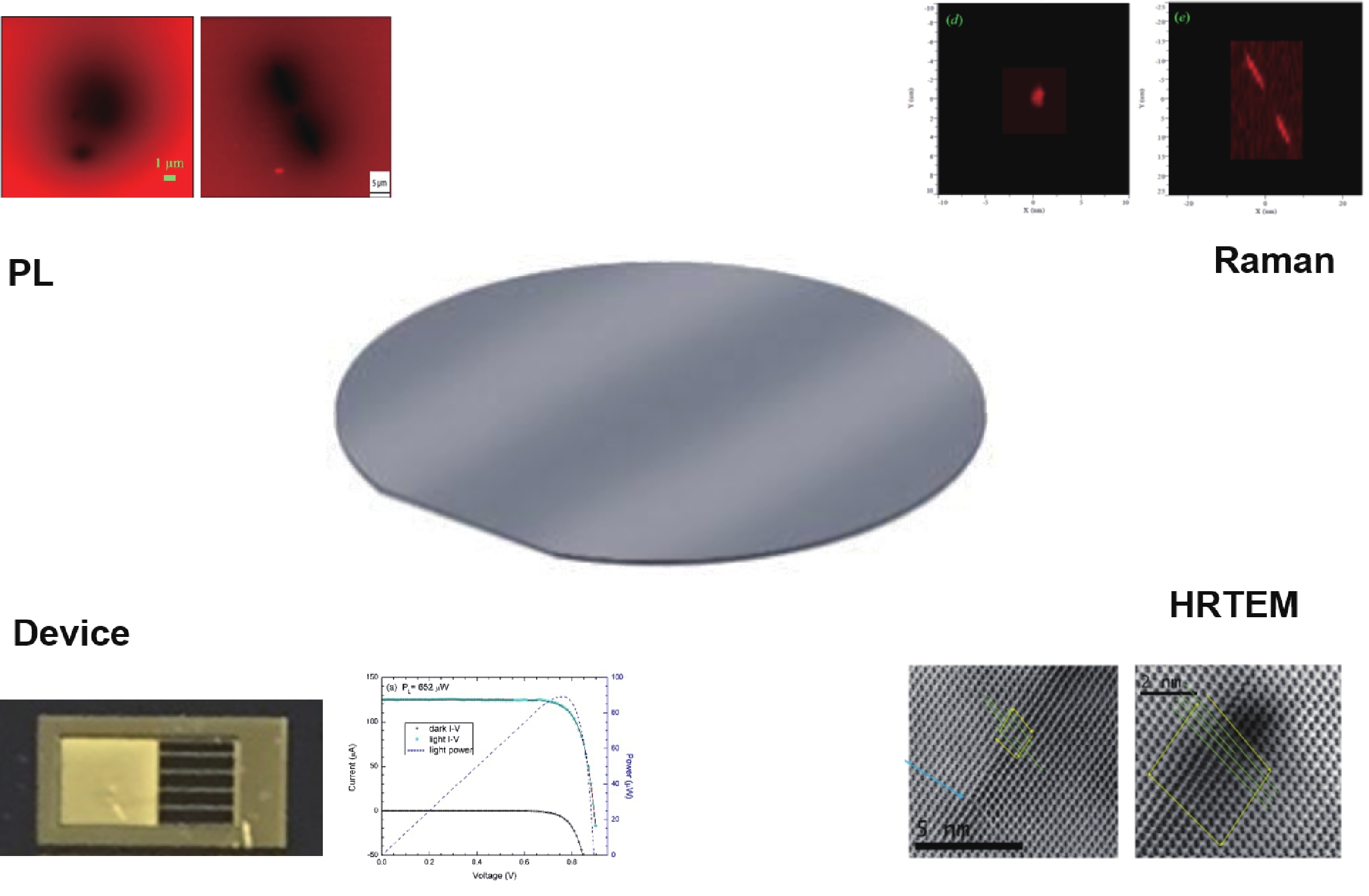
Fig. 1.
(Color online) The parallel mode of defect characterization – wafer is cut into pieces for separate studies. Examples used are only for demonstration purposes. They are not necessarily obtained from the same wafer.
REVIEWS
Yong Zhang1, and David J. Smith2,
Corresponding author: Yong Zhang, yong.zhang@uncc.edu; David J. Smith, dsmith1@asu.edu
Abstract: Despite the long history of research that has focused on the role of defects on device performance, the studies have not always been fruitful. A major reason is because these defect studies have typically been conducted in a parallel mode wherein the semiconductor wafer was divided into multiple pieces for separate optical and structural characterization, as well as device fabrication and evaluation. The major limitation of this approach was that either the defect being investigated by structural characterization techniques was not the same defect that was affecting the device performance or else the defect was not characterized under normal device operating conditions. In this review, we describe a more comprehensive approach to defect study, namely a series mode, using an array of spatially-resolved optical, electrical, and structural characterization techniques, all at the individual defect level but applied sequentially on a fabricated device. This novel sequential approach enables definitive answers to key questions, such as: (i) how do individual defects affect device performance? (ii) how does the impact depend on the device operation conditions? (iii) how does the impact vary from one defect to another? Implementation of this different approach is illustrated by the study of individual threading dislocation defects in GaAs solar cells. Additionally, we briefly describe a 3-D Raman thermometry method that can also be used for investigating the roles of defects in high power devices and device failure mechanisms.
Keywords: device performance, point defects, extended defects
| [1] |
Kittel C. Introduction to solid state physics. John Wiley & Sons, Inc, 2005
|
| [2] |
Lannoo M, Bourgoin J. Point defects in semiconductors I. Berlin, Heidelberg: Springer Berlin Heidelberg, 1981
|
| [3] |
Bourgoin J, Lannoo M. Point defects in semiconductors II. Berlin, Heidelberg: Springer Berlin Heidelberg, 1983
|
| [4] |
Holt D B, Yacobi B G. Extended defects in semiconductors. Cambridge: Cambridge University Press, 2007
|
| [5] |
Gfroerer T H, Zhang Y, Wanlass M W. An extended defect as a sensor for free carrier diffusion in a semiconductor. Appl Phys Lett, 2013, 102, 012114 doi: 10.1063/1.4775369
|
| [6] |
Zhang F, Castaneda J F, Chen S S, et al. Comparative studies of optoelectrical properties of prominent PV materials: Halide perovskite, CdTe, and GaAs. Mater Today, 2020, 36, 18 doi: 10.1016/j.mattod.2020.01.001
|
| [7] |
Lin Y, Zhang Y, Liu Z Q, et al. Interplay of point defects, extended defects, and carrier localization in the efficiency droop of InGaN quantum wells light-emitting diodes investigated using spatially resolved electroluminescence and photoluminescence. J Appl Phys, 2014, 115, 023103 doi: 10.1063/1.4861150
|
| [8] |
Petroff P, Hartman R L. Defect structure introduced during operation of heterojunction GaAs lasers. Appl Phys Lett, 1973, 23, 469 doi: 10.1063/1.1654962
|
| [9] |
Kurtsiefer C, Mayer S, Zarda P, et al. Stable solid-state source of single photons. Phys Rev Lett, 2000, 85, 290 doi: 10.1103/PhysRevLett.85.290
|
| [10] |
Francoeur S, Klem J F, Mascarenhas A. Optical spectroscopy of single impurity centers in semiconductors. Phys Rev Lett, 2004, 93, 067403 doi: 10.1103/PhysRevLett.93.067403
|
| [11] |
Romero M J, Du H, Teeter G, et al. Comparative study of the luminescence and intrinsic point defects in the kesterite Cu2ZnSnS4 and chalcopyrite Cu(In, Ga)Se2 thin films used in photovoltaic applications. Phys Rev B, 2011, 84, 165324 doi: 10.1103/PhysRevB.84.165324
|
| [12] |
Alberi K, Fluegel B, Moutinho H, et al. Measuring long-range carrier diffusion across multiple grains in polycrystalline semiconductors by photoluminescence imaging. Nat Commun, 2013, 4, 2699 doi: 10.1038/ncomms3699
|
| [13] |
Liu H N, Zhang Y, Chen Y P, et al. Confocal micro-PL mapping of defects in CdTe epilayers grown on Si (211) substrates with different annealing cycles. J Electron Mater, 2014, 43, 2854 doi: 10.1007/s11664-014-3129-y
|
| [14] |
Fluegel B, Alberi K, DiNezza M J, et al. Carrier decay and diffusion dynamics in single-crystalline CdTe as seen via microphotoluminescence. Phys Rev Applied, 2014, 2, 034010 doi: 10.1103/PhysRevApplied.2.034010
|
| [15] |
Kuciauskas D, Myers T H, Barnes T M, et al. Time-resolved correlative optical microscopy of charge-carrier transport, recombination, and space-charge fields in CdTe heterostructures. Appl Phys Lett, 2017, 110, 083905 doi: 10.1063/1.4976696
|
| [16] |
Xu X, Beckman S P, Specht P, et al. Distortion and segregation in a dislocation core region at atomic resolution. Phys Rev Lett, 2005, 95, 145501 doi: 10.1103/PhysRevLett.95.145501
|
| [17] |
Smith D J, Aoki T, Mardinly J, et al. Exploring aberration-corrected electron microscopy for compound semiconductors. Microscopy, 2013, 62, S65 doi: 10.1093/jmicro/dft011
|
| [18] |
Li C, Wu Y L, Pennycook T J, et al. Carrier separation at dislocation pairs in CdTe. Phys Rev Lett, 2013, 111, 096403 doi: 10.1103/PhysRevLett.111.096403
|
| [19] |
Hauer B, Marvinney C E, Lewin M, et al. Exploiting phonon-resonant near-field interaction for the nanoscale investigation of extended defects. Adv Funct Mater, 2020, 30, 1907357 doi: 10.1002/adfm.201907357
|
| [20] |
Chen Q, McKeon B S, Zhang S Y, et al. Impact of individual structural defects in GaAs solar cells: A correlative and in operando investigation of signatures, structures, and effects. Adv Opt Mater, 2021, 9, 2001487 doi: 10.1002/adom.202001487
|
| [21] |
Chen Q, McKeon B S, Becker J, et al. Correlative characterization of dislocation defects and defect clusters in GaAs and CdTe solar cells by spatially resolved optical techniques and high-resolution TEM. 2018 IEEE 7th World Conference on Photovoltaic Energy Conversion, 2018, 3234
|
| [22] |
Chen Q, Zhang Y. The reversal of the laser-beam-induced-current contrast with varying illumination density in a Cu2ZnSnSe4 thin-film solar cell. Appl Phys Lett, 2013, 103, 242104 doi: 10.1063/1.4844815
|
| [23] |
Lin C H, Merz T A, Doutt D R, et al. Strain and temperature dependence of defect formation at AlGaN/GaN high-electron-mobility transistors on a nanometer scale. IEEE Trans Electron Devices, 2012, 59, 2667 doi: 10.1109/TED.2012.2206595
|
| [24] |
Park T, Guan Y J, Liu Z Q, et al. In operando micro-Raman three-dimensional thermometry with diffraction-limit spatial resolution for GaN-based light-emitting diodes. Phys Rev Appl, 2018, 10, 034049 doi: 10.1103/PhysRevApplied.10.034049
|
| [25] |
Chen F, Zhang Y, Gfroerer T H, et al. Spatial resolution versus data acquisition efficiency in mapping an inhomogeneous system with species diffusion. Sci Rep, 2015, 5, 10542 doi: 10.1038/srep10542
|
| [26] |
Hu C, Chen Q, Chen F, et al. Overcoming diffusion-related limitations in semiconductor defect imaging with phonon-plasmon-coupled mode Raman scattering. Light Sci Appl, 2018, 7, 23 doi: 10.1038/s41377-018-0016-y
|
| [27] |
Irmer G, Wenzel M, Monecke J. Light scattering by a multicomponent plasma coupled with longitudinal-optical phonons: Raman spectra ofp-type GaAs:Zn. Phys Rev B, 1997, 56, 9524 doi: 10.1103/PhysRevB.56.9524
|
| [28] |
Mooradian A, Wright G B. Observation of the interaction of plasmons with longitudinal optical phonons in GaAs. Phys Rev Lett, 1966, 16, 999 doi: 10.1103/PhysRevLett.16.999
|
| [29] |
Green M A. Silicon solar cells. University of New South Wales, Sydney, 1995
|
| [30] |
Paetzold O, Irmer G, Monecke J, et al. Micro Raman study of dislocations in n-type doped GaAs. J Raman Spectrosc, 1993, 24, 761 doi: 10.1002/jrs.1250241107
|
| [31] |
Martín P, Jiménez J, Frigeri C, et al. A study of the dislocations in Si-doped GaAs comparing diluted Sirtl light etching, electron-beam-induced current, and micro-Raman techniques. J Mater Res, 1999, 14, 1732 doi: 10.1557/JMR.1999.0235
|
| [32] |
Chang K S, Yang S C, Kim J Y, et al. Precise temperature mapping of GaN-based LEDs by quantitative infrared micro-thermography. Sensors, 2012, 12, 4648 doi: 10.3390/s120404648
|
| [33] |
Wu D T, Busse G. Lock-in thermography for nondestructive evaluation of materials. Revue Générale De Thermique, 1998, 37, 693
|
| [34] |
Dallas J, Pavlidis G, Chatterjee B, et al. Thermal characterization of gallium nitride p-i-n diodes. Appl Phys Lett, 2018, 112, 073503 doi: 10.1063/1.5006796
|
| [35] |
Senawiratne J, Li Y, Zhu M, et al. Junction temperature measurements and thermal modeling of GaInN/GaN quantum well light-emitting diodes. J Electron Mater, 2008, 37, 607 doi: 10.1007/s11664-007-0370-7
|
| [36] |
Lin Y, Zhang Y, Liu Z, et al. Spatially resolved study of quantum efficiency droop in InGaN light-emitting diodes. Appl Phys Lett, 2012, 101, 252103 doi: 10.1063/1.4772549
|
| [37] |
Peri P, Fu K, Fu H Q, et al. Structural breakdown in high power GaN-on-GaN p-n diode devices stressed to failure. J Vac Sci Technol A, 2020, 38, 063402 doi: 10.1116/6.0000488
|

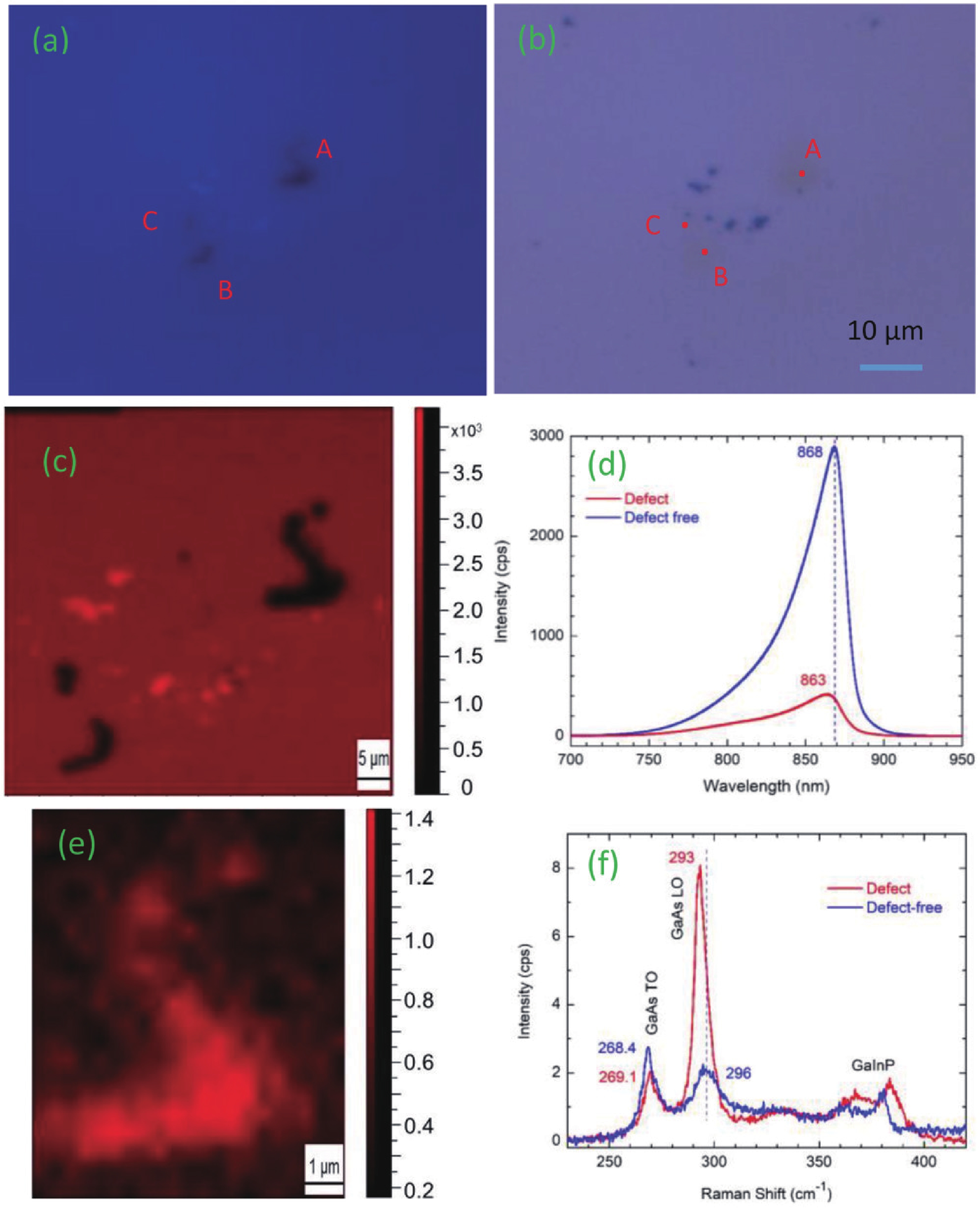
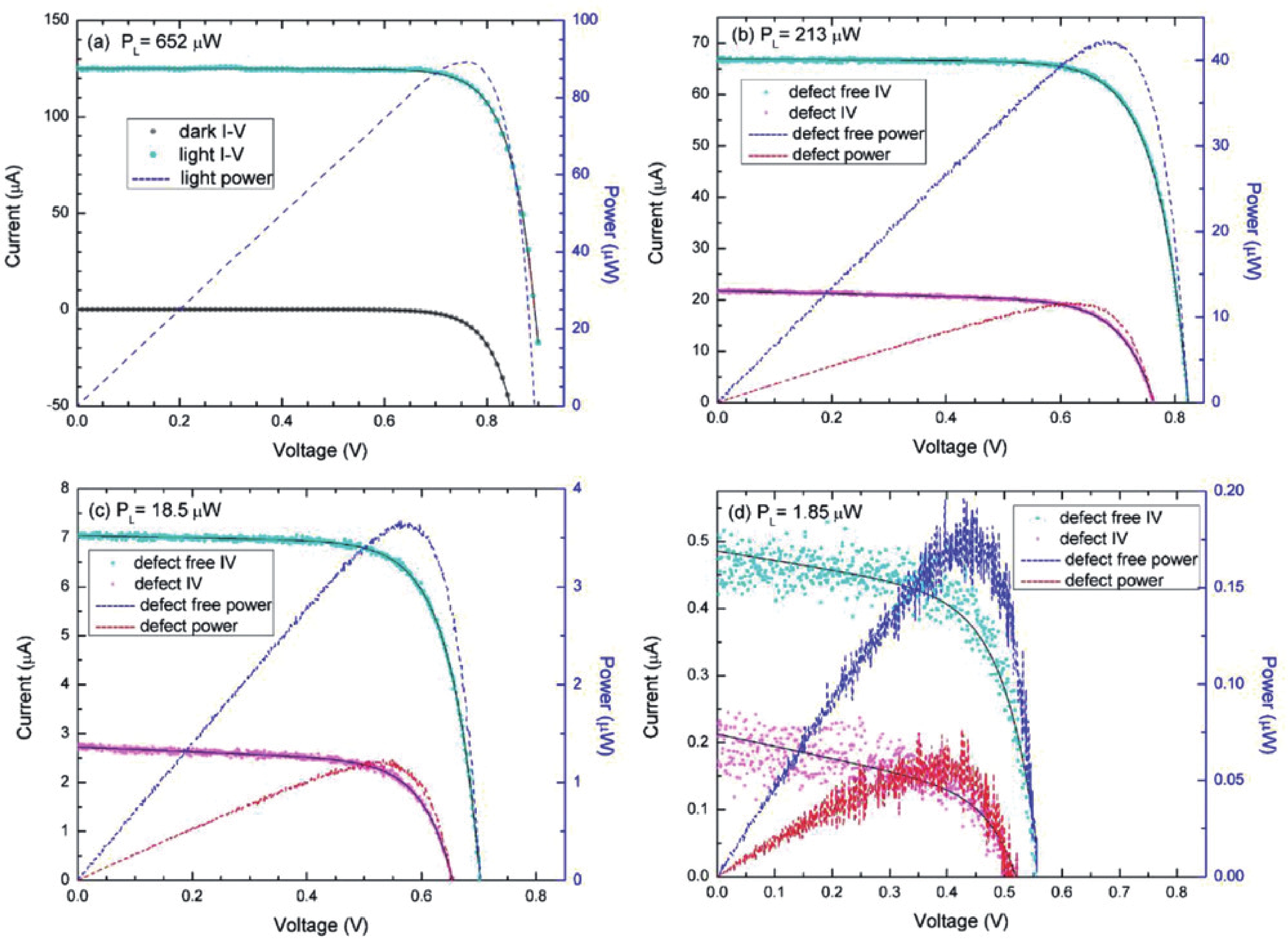
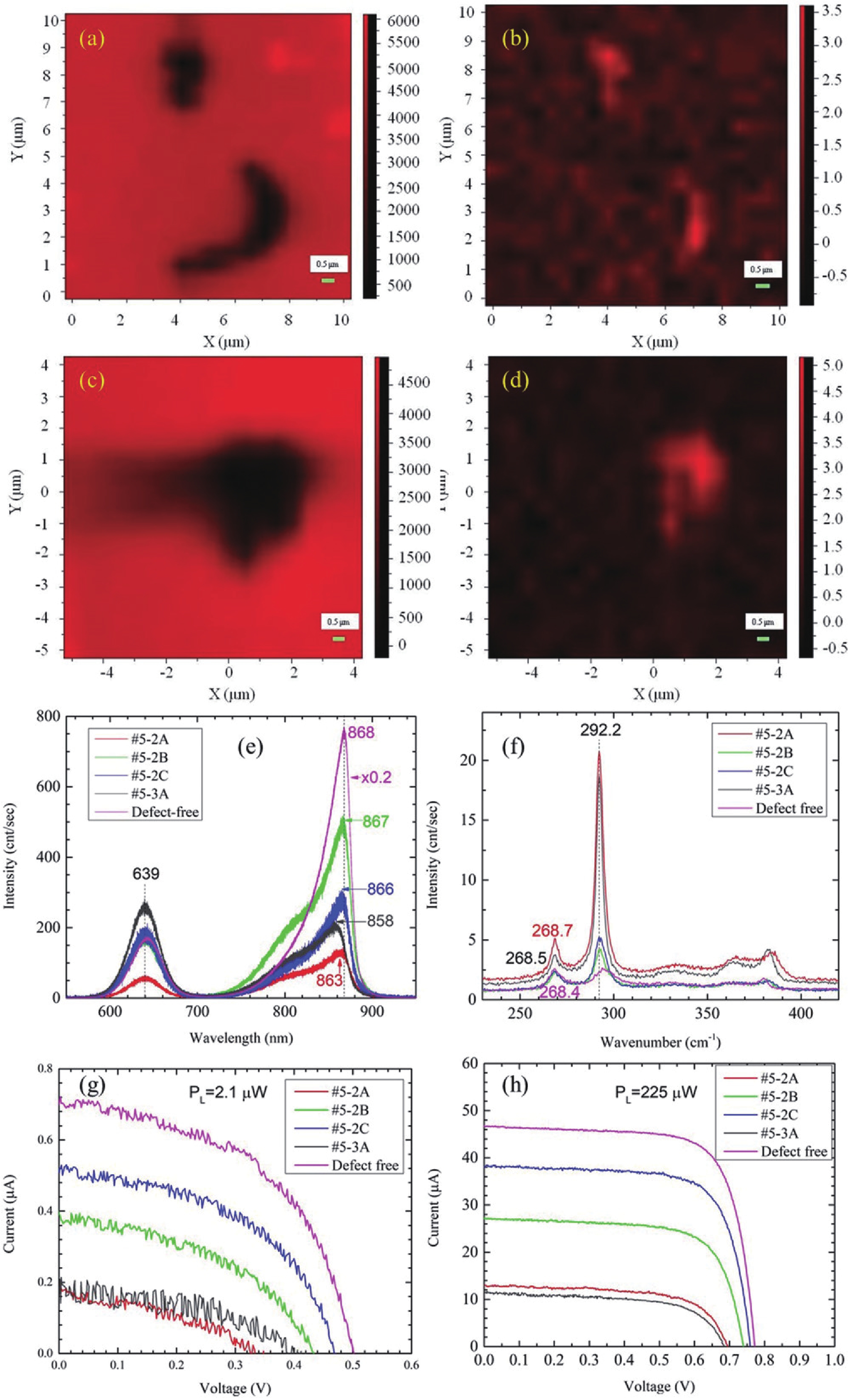
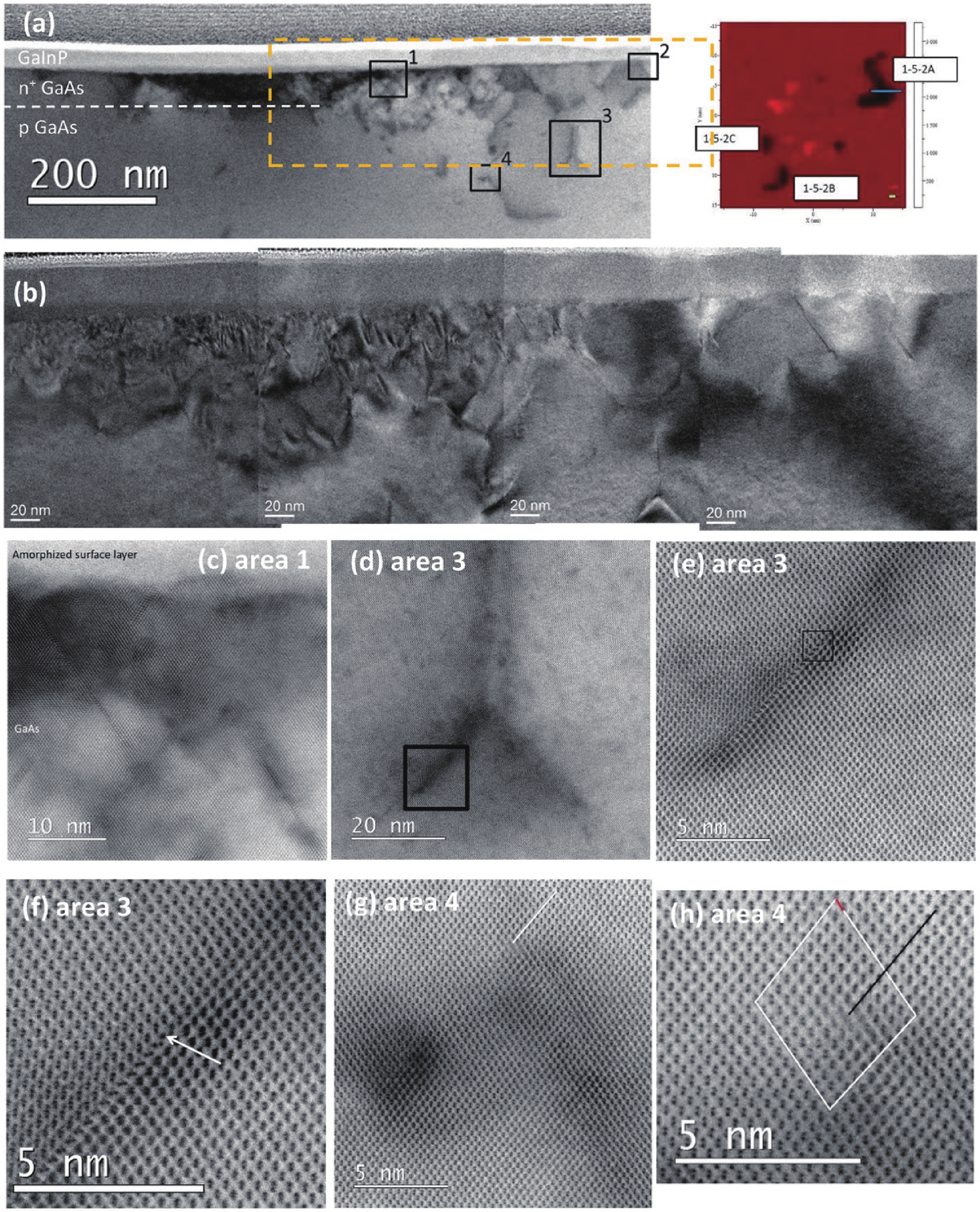
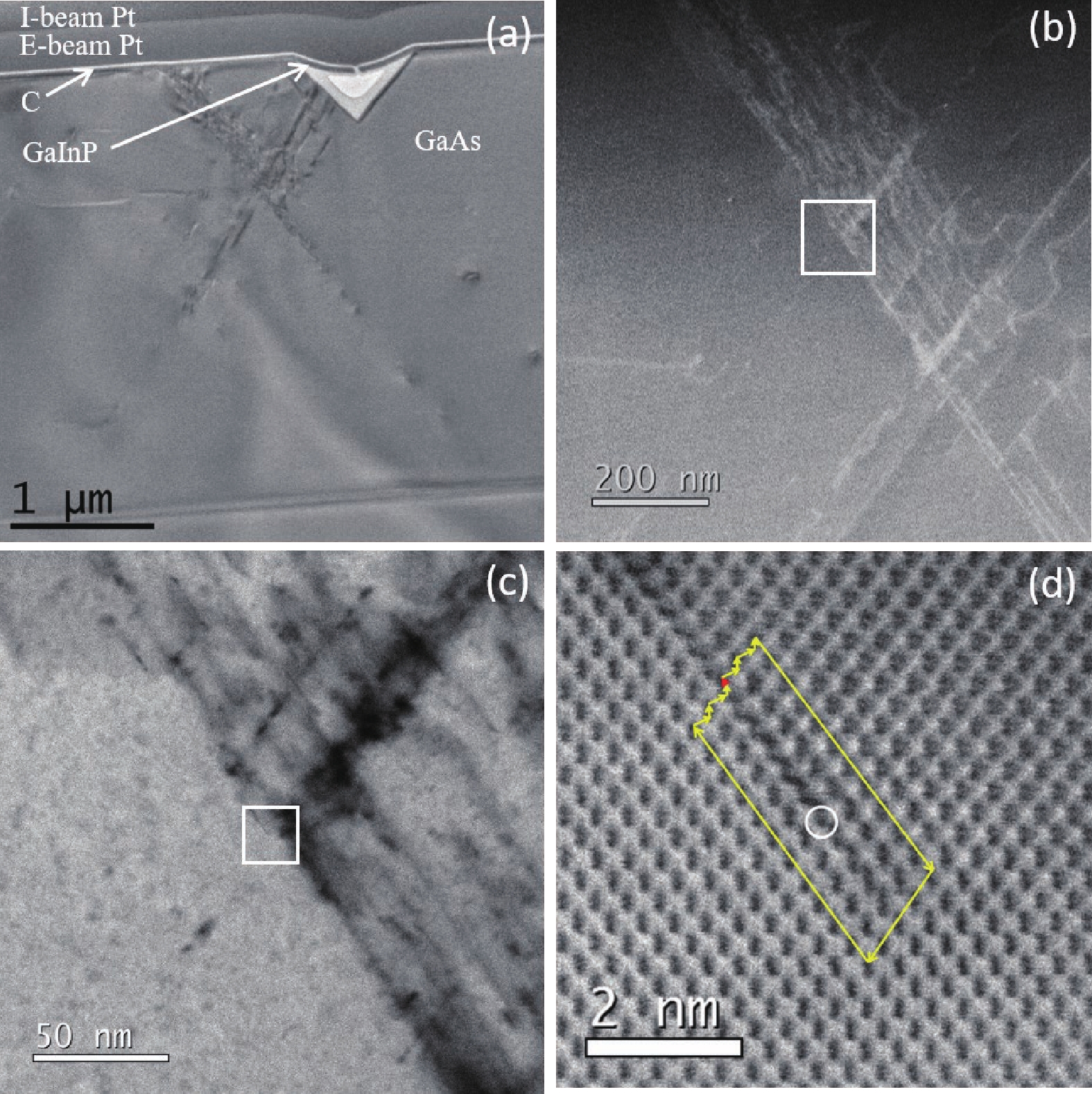
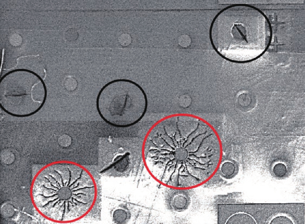
Table 1. Summary of characterization results for defect #5-2A. The first row is for the macroscopic results of #5 as a whole, measured under approximate 1 sun (~850 W/m2). The remaining rows are microscopic results measured using a diffraction-limit laser beam of 532 nm. The error bars are given as superscripts for the key parameters. The efficiency values in parentheses have been corrected for the reflectance loss (R = 0.29 @532 nm). (reproduced with permission[20])
| PL (µW) | Site | Isc (µA) | Voc (mV) | FF | η (%) | I0 (pA) | n | Rsh (MΩ) | Rs (10–3 Ω) |
| 652 | Whole cell | 125 ± 0.2 | 893 ± 0.1 | 0.799 ± 0.003 | 13.7 ± 0.1 (~19.3) | 0.778 | 1.83 | 4.75 | 0.90 |
| 213 | Defect-free | 66.9 ± 0.3 | 822 ± 0.5 | 0.766 ± 0.007 | 19.8 ± 0.1 (27.9) | 17.9 | 2.11 | 1.57 | 3.93 |
| Defect | 21.7 ± 0.3 | 762 ± 0.5 | 0.708 ± 0.02 | 5.49 ± 0.1 (7.73) | 20.1 | 2.15 | 0.356 | 3.82 | |
| 18.5 | Defect-free | 7.03 ± 0.02 | 701 ± 0.5 | 0.728 ± 0.011 | 19.4 ± 0.2 (27.3) | 11.1 | 2.04 | 4.76 | 1.71 |
| Defect | 2.72 ± 0.02 | 655 ± 0.5 | 0.674 ± 0.022 | 6.49 ± 0.16 (9.14) | 7.88 | 2.01 | 2.08 | 6.43 | |
| 1.82 | Defect-free | 0.468 ± 0.04 | 556 ± 2 | 0.653 ± 0.067 | 9.34 ± 0.55 (13.2) | 21.0 | 2.21 | 7.09 | 4.82 |
| Defect | 0.194 ± 0.04 | 510 ± 8 | 0.546 ± 0.146 | 2.97 ± 0.44 (4.18) | 5.11 | 2.05 | 5.08 | 2.83 |
 DownLoad: CSV
| [1] |
Kittel C. Introduction to solid state physics. John Wiley & Sons, Inc, 2005
|
| [2] |
Lannoo M, Bourgoin J. Point defects in semiconductors I. Berlin, Heidelberg: Springer Berlin Heidelberg, 1981
|
| [3] |
Bourgoin J, Lannoo M. Point defects in semiconductors II. Berlin, Heidelberg: Springer Berlin Heidelberg, 1983
|
| [4] |
Holt D B, Yacobi B G. Extended defects in semiconductors. Cambridge: Cambridge University Press, 2007
|
| [5] |
Gfroerer T H, Zhang Y, Wanlass M W. An extended defect as a sensor for free carrier diffusion in a semiconductor. Appl Phys Lett, 2013, 102, 012114 doi: 10.1063/1.4775369
|
| [6] |
Zhang F, Castaneda J F, Chen S S, et al. Comparative studies of optoelectrical properties of prominent PV materials: Halide perovskite, CdTe, and GaAs. Mater Today, 2020, 36, 18 doi: 10.1016/j.mattod.2020.01.001
|
| [7] |
Lin Y, Zhang Y, Liu Z Q, et al. Interplay of point defects, extended defects, and carrier localization in the efficiency droop of InGaN quantum wells light-emitting diodes investigated using spatially resolved electroluminescence and photoluminescence. J Appl Phys, 2014, 115, 023103 doi: 10.1063/1.4861150
|
| [8] |
Petroff P, Hartman R L. Defect structure introduced during operation of heterojunction GaAs lasers. Appl Phys Lett, 1973, 23, 469 doi: 10.1063/1.1654962
|
| [9] |
Kurtsiefer C, Mayer S, Zarda P, et al. Stable solid-state source of single photons. Phys Rev Lett, 2000, 85, 290 doi: 10.1103/PhysRevLett.85.290
|
| [10] |
Francoeur S, Klem J F, Mascarenhas A. Optical spectroscopy of single impurity centers in semiconductors. Phys Rev Lett, 2004, 93, 067403 doi: 10.1103/PhysRevLett.93.067403
|
| [11] |
Romero M J, Du H, Teeter G, et al. Comparative study of the luminescence and intrinsic point defects in the kesterite Cu2ZnSnS4 and chalcopyrite Cu(In, Ga)Se2 thin films used in photovoltaic applications. Phys Rev B, 2011, 84, 165324 doi: 10.1103/PhysRevB.84.165324
|
| [12] |
Alberi K, Fluegel B, Moutinho H, et al. Measuring long-range carrier diffusion across multiple grains in polycrystalline semiconductors by photoluminescence imaging. Nat Commun, 2013, 4, 2699 doi: 10.1038/ncomms3699
|
| [13] |
Liu H N, Zhang Y, Chen Y P, et al. Confocal micro-PL mapping of defects in CdTe epilayers grown on Si (211) substrates with different annealing cycles. J Electron Mater, 2014, 43, 2854 doi: 10.1007/s11664-014-3129-y
|
| [14] |
Fluegel B, Alberi K, DiNezza M J, et al. Carrier decay and diffusion dynamics in single-crystalline CdTe as seen via microphotoluminescence. Phys Rev Applied, 2014, 2, 034010 doi: 10.1103/PhysRevApplied.2.034010
|
| [15] |
Kuciauskas D, Myers T H, Barnes T M, et al. Time-resolved correlative optical microscopy of charge-carrier transport, recombination, and space-charge fields in CdTe heterostructures. Appl Phys Lett, 2017, 110, 083905 doi: 10.1063/1.4976696
|
| [16] |
Xu X, Beckman S P, Specht P, et al. Distortion and segregation in a dislocation core region at atomic resolution. Phys Rev Lett, 2005, 95, 145501 doi: 10.1103/PhysRevLett.95.145501
|
| [17] |
Smith D J, Aoki T, Mardinly J, et al. Exploring aberration-corrected electron microscopy for compound semiconductors. Microscopy, 2013, 62, S65 doi: 10.1093/jmicro/dft011
|
| [18] |
Li C, Wu Y L, Pennycook T J, et al. Carrier separation at dislocation pairs in CdTe. Phys Rev Lett, 2013, 111, 096403 doi: 10.1103/PhysRevLett.111.096403
|
| [19] |
Hauer B, Marvinney C E, Lewin M, et al. Exploiting phonon-resonant near-field interaction for the nanoscale investigation of extended defects. Adv Funct Mater, 2020, 30, 1907357 doi: 10.1002/adfm.201907357
|
| [20] |
Chen Q, McKeon B S, Zhang S Y, et al. Impact of individual structural defects in GaAs solar cells: A correlative and in operando investigation of signatures, structures, and effects. Adv Opt Mater, 2021, 9, 2001487 doi: 10.1002/adom.202001487
|
| [21] |
Chen Q, McKeon B S, Becker J, et al. Correlative characterization of dislocation defects and defect clusters in GaAs and CdTe solar cells by spatially resolved optical techniques and high-resolution TEM. 2018 IEEE 7th World Conference on Photovoltaic Energy Conversion, 2018, 3234
|
| [22] |
Chen Q, Zhang Y. The reversal of the laser-beam-induced-current contrast with varying illumination density in a Cu2ZnSnSe4 thin-film solar cell. Appl Phys Lett, 2013, 103, 242104 doi: 10.1063/1.4844815
|
| [23] |
Lin C H, Merz T A, Doutt D R, et al. Strain and temperature dependence of defect formation at AlGaN/GaN high-electron-mobility transistors on a nanometer scale. IEEE Trans Electron Devices, 2012, 59, 2667 doi: 10.1109/TED.2012.2206595
|
| [24] |
Park T, Guan Y J, Liu Z Q, et al. In operando micro-Raman three-dimensional thermometry with diffraction-limit spatial resolution for GaN-based light-emitting diodes. Phys Rev Appl, 2018, 10, 034049 doi: 10.1103/PhysRevApplied.10.034049
|
| [25] |
Chen F, Zhang Y, Gfroerer T H, et al. Spatial resolution versus data acquisition efficiency in mapping an inhomogeneous system with species diffusion. Sci Rep, 2015, 5, 10542 doi: 10.1038/srep10542
|
| [26] |
Hu C, Chen Q, Chen F, et al. Overcoming diffusion-related limitations in semiconductor defect imaging with phonon-plasmon-coupled mode Raman scattering. Light Sci Appl, 2018, 7, 23 doi: 10.1038/s41377-018-0016-y
|
| [27] |
Irmer G, Wenzel M, Monecke J. Light scattering by a multicomponent plasma coupled with longitudinal-optical phonons: Raman spectra ofp-type GaAs:Zn. Phys Rev B, 1997, 56, 9524 doi: 10.1103/PhysRevB.56.9524
|
| [28] |
Mooradian A, Wright G B. Observation of the interaction of plasmons with longitudinal optical phonons in GaAs. Phys Rev Lett, 1966, 16, 999 doi: 10.1103/PhysRevLett.16.999
|
| [29] |
Green M A. Silicon solar cells. University of New South Wales, Sydney, 1995
|
| [30] |
Paetzold O, Irmer G, Monecke J, et al. Micro Raman study of dislocations in n-type doped GaAs. J Raman Spectrosc, 1993, 24, 761 doi: 10.1002/jrs.1250241107
|
| [31] |
Martín P, Jiménez J, Frigeri C, et al. A study of the dislocations in Si-doped GaAs comparing diluted Sirtl light etching, electron-beam-induced current, and micro-Raman techniques. J Mater Res, 1999, 14, 1732 doi: 10.1557/JMR.1999.0235
|
| [32] |
Chang K S, Yang S C, Kim J Y, et al. Precise temperature mapping of GaN-based LEDs by quantitative infrared micro-thermography. Sensors, 2012, 12, 4648 doi: 10.3390/s120404648
|
| [33] |
Wu D T, Busse G. Lock-in thermography for nondestructive evaluation of materials. Revue Générale De Thermique, 1998, 37, 693
|
| [34] |
Dallas J, Pavlidis G, Chatterjee B, et al. Thermal characterization of gallium nitride p-i-n diodes. Appl Phys Lett, 2018, 112, 073503 doi: 10.1063/1.5006796
|
| [35] |
Senawiratne J, Li Y, Zhu M, et al. Junction temperature measurements and thermal modeling of GaInN/GaN quantum well light-emitting diodes. J Electron Mater, 2008, 37, 607 doi: 10.1007/s11664-007-0370-7
|
| [36] |
Lin Y, Zhang Y, Liu Z, et al. Spatially resolved study of quantum efficiency droop in InGaN light-emitting diodes. Appl Phys Lett, 2012, 101, 252103 doi: 10.1063/1.4772549
|
| [37] |
Peri P, Fu K, Fu H Q, et al. Structural breakdown in high power GaN-on-GaN p-n diode devices stressed to failure. J Vac Sci Technol A, 2020, 38, 063402 doi: 10.1116/6.0000488
|


Article views: 3217 Times PDF downloads: 123 Times Cited by: 0 Times
Received: 25 February 2022 Revised: 17 March 2022 Online: Accepted Manuscript: 26 March 2022Uncorrected proof: 28 March 2022Published: 18 April 2022
| Citation: |
Yong Zhang, David J. Smith. Comprehensive, in operando, and correlative investigation of defects and their impact on device performance[J]. Journal of Semiconductors, 2022, 43(4): 041102. doi: 10.1088/1674-4926/43/4/041102
****
Y Zhang, D J Smith. Comprehensive, in operando, and correlative investigation of defects and their impact on device performance[J]. J. Semicond, 2022, 43(4): 041102. doi: 10.1088/1674-4926/43/4/041102

|
| [1] |
Kittel C. Introduction to solid state physics. John Wiley & Sons, Inc, 2005
|
| [2] |
Lannoo M, Bourgoin J. Point defects in semiconductors I. Berlin, Heidelberg: Springer Berlin Heidelberg, 1981
|
| [3] |
Bourgoin J, Lannoo M. Point defects in semiconductors II. Berlin, Heidelberg: Springer Berlin Heidelberg, 1983
|
| [4] |
Holt D B, Yacobi B G. Extended defects in semiconductors. Cambridge: Cambridge University Press, 2007
|
| [5] |
Gfroerer T H, Zhang Y, Wanlass M W. An extended defect as a sensor for free carrier diffusion in a semiconductor. Appl Phys Lett, 2013, 102, 012114 doi: 10.1063/1.4775369
|
| [6] |
Zhang F, Castaneda J F, Chen S S, et al. Comparative studies of optoelectrical properties of prominent PV materials: Halide perovskite, CdTe, and GaAs. Mater Today, 2020, 36, 18 doi: 10.1016/j.mattod.2020.01.001
|
| [7] |
Lin Y, Zhang Y, Liu Z Q, et al. Interplay of point defects, extended defects, and carrier localization in the efficiency droop of InGaN quantum wells light-emitting diodes investigated using spatially resolved electroluminescence and photoluminescence. J Appl Phys, 2014, 115, 023103 doi: 10.1063/1.4861150
|
| [8] |
Petroff P, Hartman R L. Defect structure introduced during operation of heterojunction GaAs lasers. Appl Phys Lett, 1973, 23, 469 doi: 10.1063/1.1654962
|
| [9] |
Kurtsiefer C, Mayer S, Zarda P, et al. Stable solid-state source of single photons. Phys Rev Lett, 2000, 85, 290 doi: 10.1103/PhysRevLett.85.290
|
| [10] |
Francoeur S, Klem J F, Mascarenhas A. Optical spectroscopy of single impurity centers in semiconductors. Phys Rev Lett, 2004, 93, 067403 doi: 10.1103/PhysRevLett.93.067403
|
| [11] |
Romero M J, Du H, Teeter G, et al. Comparative study of the luminescence and intrinsic point defects in the kesterite Cu2ZnSnS4 and chalcopyrite Cu(In, Ga)Se2 thin films used in photovoltaic applications. Phys Rev B, 2011, 84, 165324 doi: 10.1103/PhysRevB.84.165324
|
| [12] |
Alberi K, Fluegel B, Moutinho H, et al. Measuring long-range carrier diffusion across multiple grains in polycrystalline semiconductors by photoluminescence imaging. Nat Commun, 2013, 4, 2699 doi: 10.1038/ncomms3699
|
| [13] |
Liu H N, Zhang Y, Chen Y P, et al. Confocal micro-PL mapping of defects in CdTe epilayers grown on Si (211) substrates with different annealing cycles. J Electron Mater, 2014, 43, 2854 doi: 10.1007/s11664-014-3129-y
|
| [14] |
Fluegel B, Alberi K, DiNezza M J, et al. Carrier decay and diffusion dynamics in single-crystalline CdTe as seen via microphotoluminescence. Phys Rev Applied, 2014, 2, 034010 doi: 10.1103/PhysRevApplied.2.034010
|
| [15] |
Kuciauskas D, Myers T H, Barnes T M, et al. Time-resolved correlative optical microscopy of charge-carrier transport, recombination, and space-charge fields in CdTe heterostructures. Appl Phys Lett, 2017, 110, 083905 doi: 10.1063/1.4976696
|
| [16] |
Xu X, Beckman S P, Specht P, et al. Distortion and segregation in a dislocation core region at atomic resolution. Phys Rev Lett, 2005, 95, 145501 doi: 10.1103/PhysRevLett.95.145501
|
| [17] |
Smith D J, Aoki T, Mardinly J, et al. Exploring aberration-corrected electron microscopy for compound semiconductors. Microscopy, 2013, 62, S65 doi: 10.1093/jmicro/dft011
|
| [18] |
Li C, Wu Y L, Pennycook T J, et al. Carrier separation at dislocation pairs in CdTe. Phys Rev Lett, 2013, 111, 096403 doi: 10.1103/PhysRevLett.111.096403
|
| [19] |
Hauer B, Marvinney C E, Lewin M, et al. Exploiting phonon-resonant near-field interaction for the nanoscale investigation of extended defects. Adv Funct Mater, 2020, 30, 1907357 doi: 10.1002/adfm.201907357
|
| [20] |
Chen Q, McKeon B S, Zhang S Y, et al. Impact of individual structural defects in GaAs solar cells: A correlative and in operando investigation of signatures, structures, and effects. Adv Opt Mater, 2021, 9, 2001487 doi: 10.1002/adom.202001487
|
| [21] |
Chen Q, McKeon B S, Becker J, et al. Correlative characterization of dislocation defects and defect clusters in GaAs and CdTe solar cells by spatially resolved optical techniques and high-resolution TEM. 2018 IEEE 7th World Conference on Photovoltaic Energy Conversion, 2018, 3234
|
| [22] |
Chen Q, Zhang Y. The reversal of the laser-beam-induced-current contrast with varying illumination density in a Cu2ZnSnSe4 thin-film solar cell. Appl Phys Lett, 2013, 103, 242104 doi: 10.1063/1.4844815
|
| [23] |
Lin C H, Merz T A, Doutt D R, et al. Strain and temperature dependence of defect formation at AlGaN/GaN high-electron-mobility transistors on a nanometer scale. IEEE Trans Electron Devices, 2012, 59, 2667 doi: 10.1109/TED.2012.2206595
|
| [24] |
Park T, Guan Y J, Liu Z Q, et al. In operando micro-Raman three-dimensional thermometry with diffraction-limit spatial resolution for GaN-based light-emitting diodes. Phys Rev Appl, 2018, 10, 034049 doi: 10.1103/PhysRevApplied.10.034049
|
| [25] |
Chen F, Zhang Y, Gfroerer T H, et al. Spatial resolution versus data acquisition efficiency in mapping an inhomogeneous system with species diffusion. Sci Rep, 2015, 5, 10542 doi: 10.1038/srep10542
|
| [26] |
Hu C, Chen Q, Chen F, et al. Overcoming diffusion-related limitations in semiconductor defect imaging with phonon-plasmon-coupled mode Raman scattering. Light Sci Appl, 2018, 7, 23 doi: 10.1038/s41377-018-0016-y
|
| [27] |
Irmer G, Wenzel M, Monecke J. Light scattering by a multicomponent plasma coupled with longitudinal-optical phonons: Raman spectra ofp-type GaAs:Zn. Phys Rev B, 1997, 56, 9524 doi: 10.1103/PhysRevB.56.9524
|
| [28] |
Mooradian A, Wright G B. Observation of the interaction of plasmons with longitudinal optical phonons in GaAs. Phys Rev Lett, 1966, 16, 999 doi: 10.1103/PhysRevLett.16.999
|
| [29] |
Green M A. Silicon solar cells. University of New South Wales, Sydney, 1995
|
| [30] |
Paetzold O, Irmer G, Monecke J, et al. Micro Raman study of dislocations in n-type doped GaAs. J Raman Spectrosc, 1993, 24, 761 doi: 10.1002/jrs.1250241107
|
| [31] |
Martín P, Jiménez J, Frigeri C, et al. A study of the dislocations in Si-doped GaAs comparing diluted Sirtl light etching, electron-beam-induced current, and micro-Raman techniques. J Mater Res, 1999, 14, 1732 doi: 10.1557/JMR.1999.0235
|
| [32] |
Chang K S, Yang S C, Kim J Y, et al. Precise temperature mapping of GaN-based LEDs by quantitative infrared micro-thermography. Sensors, 2012, 12, 4648 doi: 10.3390/s120404648
|
| [33] |
Wu D T, Busse G. Lock-in thermography for nondestructive evaluation of materials. Revue Générale De Thermique, 1998, 37, 693
|
| [34] |
Dallas J, Pavlidis G, Chatterjee B, et al. Thermal characterization of gallium nitride p-i-n diodes. Appl Phys Lett, 2018, 112, 073503 doi: 10.1063/1.5006796
|
| [35] |
Senawiratne J, Li Y, Zhu M, et al. Junction temperature measurements and thermal modeling of GaInN/GaN quantum well light-emitting diodes. J Electron Mater, 2008, 37, 607 doi: 10.1007/s11664-007-0370-7
|
| [36] |
Lin Y, Zhang Y, Liu Z, et al. Spatially resolved study of quantum efficiency droop in InGaN light-emitting diodes. Appl Phys Lett, 2012, 101, 252103 doi: 10.1063/1.4772549
|
| [37] |
Peri P, Fu K, Fu H Q, et al. Structural breakdown in high power GaN-on-GaN p-n diode devices stressed to failure. J Vac Sci Technol A, 2020, 38, 063402 doi: 10.1116/6.0000488
|

 WeChat ID
Journal of Semiconductors © 2017 All Rights Reserved 京ICP备05085259号-2


