| Citation: |
Min Wu, Weida Hong, Guanyu Liu, Jiejun Zhang, Ziao Tian, Miao Zhang. Double-balanced mixer based on monolayer graphene field-effect transistors[J]. Journal of Semiconductors, 2022, 43(5): 052002. doi: 10.1088/1674-4926/43/5/052002
****
M Wu, W D Hong, G Y Liu, J J Zhang, Z A Tian, M Zhang. Double-balanced mixer based on monolayer graphene field-effect transistors[J]. J. Semicond, 2022, 43(5): 052002. doi: 10.1088/1674-4926/43/5/052002
|
Double-balanced mixer based on monolayer graphene field-effect transistors
DOI: 10.1088/1674-4926/43/5/052002
More Information
-
Abstract
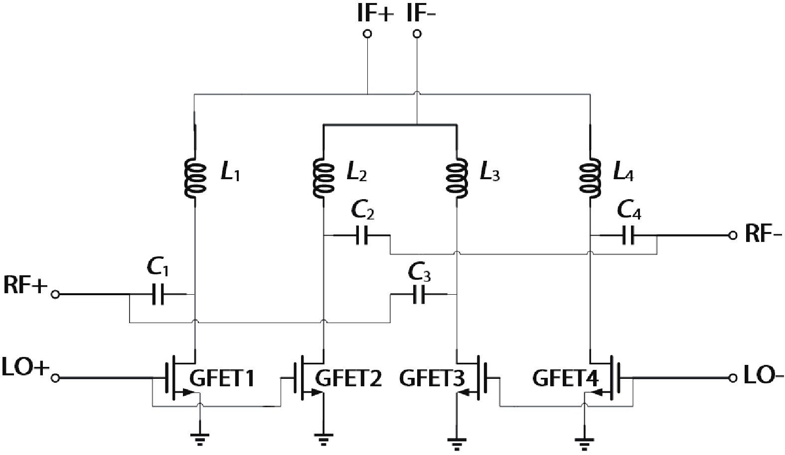
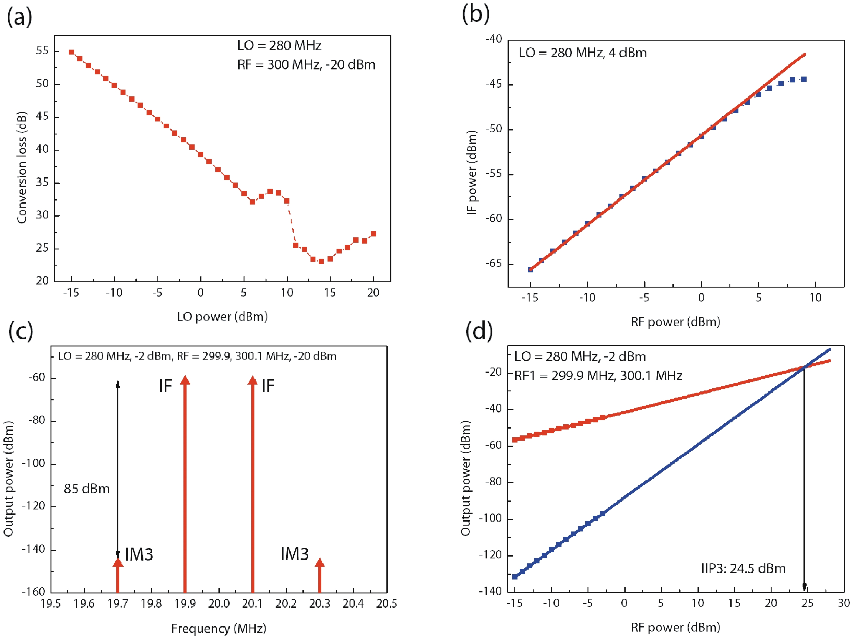
Graphene field-effect transistors (GFET) have attracted much attention in the radio frequency (RF) and microwave fields because of its extremely high carrier mobility. In this paper, a GFET with a gate length of 5 μm is fabricated through the van der Walls (vdW) transfer process, and then the existing large-signal GFET model is described, and the model is implemented in Verilog-A for analysis in RF and microwave circuits. Next a double-balanced mixer based on four GFETs is designed and analyzed in advanced design system (ADS) tools. Finally, the simulation results show that with the input of 300 and 280 MHz, the IIP3 of the mixed signal is 24.5 dBm.-
Keywords:
- GFET,
- mixer,
- RF,
- simulation,
- IIP3
-
References
[1] Novoselov K S, Geim A K, Morozov S V, et al. Electric field effect in atomically thin carbon films. Science, 2004, 306, 666 doi: 10.1126/science.1102896[2] Bolotin K I, Sikes K J, Jiang Z, et al. Ultrahigh electron mobility in suspended graphene. Solid State Commun, 2008, 146, 351 doi: 10.1016/j.ssc.2008.02.024[3] Du X, Skachko I, Barker A, et al. Approaching ballistic transport in suspended graphene. Nat Nanotechnol, 2008, 3, 491 doi: 10.1038/nnano.2008.199[4] Hong X, Posadas A, Zou K, et al. High-mobility few-layer graphene field effect transistors fabricated on epitaxial ferroelectric gate oxides. Phys Rev Lett, 2009, 102, 136808 doi: 10.1103/PhysRevLett.102.136808[5] Dorgan V E, Bae M H, Pop E. Mobility and saturation velocity in graphene on SiO2. Appl Phys Lett, 2010, 97, 082112 doi: 10.1063/1.3483130[6] Kuhn K J. Considerations for ultimate CMOS scaling. IEEE Trans Electron Devices, 2012, 59, 1813 doi: 10.1109/TED.2012.2193129[7] Lemme M C, Echtermeyer T J, Baus M, et al. A graphene field-effect device. IEEE Electron Device Lett, 2007, 28, 282 doi: 10.1109/LED.2007.891668[8] Wang H, Nezich D, Kong J, et al. Graphene frequency multipliers. IEEE Electron Device Lett, 2009, 30, 547 doi: 10.1109/LED.2009.2016443[9] Andersson M A, Habibpour O, Vukusic J, et al. 10 dB small-signal graphene FET amplifier. Electron Lett, 2012, 48, 861 doi: 10.1049/el.2012.1347[10] Iannazzo M, Muzzo V L, Rodriguez S, et al. Design exploration of graphene-FET based ring-oscillator circuits: A test-bench for large-signal compact models. 2015 IEEE International Symposium on Circuits and Systems, 2015, 2716[11] Andersson M A, Habibpour O, Vukusic J, et al. Resistive graphene FET subharmonic mixers: Noise and linearity assessment. IEEE Trans Microw Theory Tech, 2012, 60, 4035 doi: 10.1109/TMTT.2012.2221141[12] Guan H, Sun H, Bao J L, et al. High-performance RF switch in 0.13 μm RF SOI process. J Semicond, 2019, 40, 022401 doi: 10.1088/1674-4926/40/2/022401[13] Yang X, Luo C, Tian X Y, et al. A revew of in situ transmission electron microscopy study on the switching mechanism and packaging reliability in non-volatile memory. J Semicond, 2021, 42, 013102 doi: 10.1088/1674-4926/42/1/013102[14] Wang H, Hsu A, Wu J, et al. Graphene-based ambipolar RF mixers. IEEE Electron Device Lett, 2010, 31, 906 doi: 10.1109/LED.2010.2052017[15] Lin Y M, Valdes-Garcia A, Han S J, et al. Wafer-scale graphene integrated circuit. Science, 2011, 332, 1294 doi: 10.1126/science.1204428[16] Moon J S, Seo H C, Antcliffe M, et al. Graphene FETs for zero-bias linear resistive FET mixers. IEEE Electron Device Lett, 2013, 34, 465 doi: 10.1109/LED.2012.2236533[17] Habibpour O, Vukusic J, Stake J. A large-signal graphene FET model. IEEE Trans Electron Devices, 2012, 59, 968 doi: 10.1109/TED.2012.2182675[18] Lee J H, Lee E K, Joo W J, et al. Wafer-scale growth of single-crystal monolayer graphene on reusable hydrogen-terminated germanium. Science, 2014, 344, 286 doi: 10.1126/science.1252268[19] Went C M, Wong J, Jahelka P R, et al. A new metal transfer process for van der Waals contacts to vertical Schottky-junction transition metal dichalcogenide photovoltaics. Sci Adv, 2019, 5, eaax6061 doi: 10.1126/sciadv.aax6061[20] Liu Y, Guo J, Zhu E, et al. Approaching the Schottky–Mott limit in van der Waals metal–semiconductor junctions. Nature, 2018, 557, 696 doi: 10.1038/s41586-018-0129-8[21] Jung Y, Choi M S, Nipane A, et al. Transferred via contacts as a platform for ideal two-dimensional transistors. Nat Electron, 2019, 2, 187 doi: 10.1038/s41928-019-0245-y[22] Wu Y, Zou X M, Sun M L, et al. 200 GHz maximum oscillation frequency in CVD graphene radio frequency transistors. ACS Appl Mater Interfaces, 2016, 8, 25645 doi: 10.1021/acsami.6b05791[23] Rodriguez S, Vaziri S, Smith A, et al. A comprehensive graphene FET model for circuit design. IEEE Trans Electron Devices, 2014, 61, 1199 doi: 10.1109/TED.2014.2302372[24] Umoh I J, Kazmierski T J, Al-Hashimi B M. Multilayer graphene FET compact circuit-level model with temperature effects. IEEE Trans Nanotechnol, 2014, 13, 805 doi: 10.1109/TNANO.2014.2323129[25] Rakheja S, Wu Y Q, Wang H, et al. An ambipolar virtual-source-based charge-current compact model for nanoscale graphene transistors. IEEE Trans Nanotechnol, 2014, 13, 1005 doi: 10.1109/TNANO.2014.2344437[26] Landauer G M, Jiménez D, González J L. An accurate and verilog-A compatible compact model for graphene field-effect transistors. IEEE Trans Nanotechnol, 2014, 13, 895 doi: 10.1109/TNANO.2014.2328782[27] Mukherjee C, Aguirre-Morales J D, Frégonèse S, et al. Versatile compact model for graphene FET targeting reliability-aware circuit design. IEEE Trans Electron Devices, 2015, 62, 757 doi: 10.1109/TED.2015.2395134[28] Lu Q, Lyu H M, Wu X M, et al. A novel graphene double-balanced passive mixer. 2018 IEEE 13th Annual International Conference on Nano/Micro Engineered and Molecular Systems, 2018, 549[29] Chen J D, Qian J B. Low-power up-conversion folded CMOS mixer for 2-12 GHz ultra-wideband applications. IET Microw Antennas Propag, 2020, 14, 1975 doi: 10.1049/iet-map.2020.0287[30] Li J, Gu Q J. 10 GHz highly linear up-conversion mixer in 65 nm CMOS. Electron Lett, 2018, 54, 804 doi: 10.1049/el.2018.0780[31] Li J B, More A, Hao S L, et al. A 10 GHz up-conversion mixer with 13.6 dBm OIP3 using regulator-based linearized gm stage and harmonic nulling. 2018 IEEE/MTT-S International Microwave Symposium - IMS, 2018, 678[32] Gou J, Xu X Y, Huang X G. Design of a low-voltage CMOS mixer with improved linearity. 2019 International Conference on IC Design and Technology, 2019, 1[33] Sharma U K, Chaturvedi A, Kumar M. A high gain down-conversion mixer in 0.18 μm CMOS technology for ultra wideband applications. 2016 3rd International Conference on Signal Processing and Integrated Networks, 2016, 586[34] Wei W, Pallecchi E, Haque S, et al. Mechanically robust 39 GHz cut-off frequency graphene field effect transistors on flexible substrates. Nanoscale, 2016, 8, 14097 doi: 10.1039/C6NR01521B -
Proportional views


 DownLoad:
