| Citation: |
Hao Wu, Xuanwu Kang, Yingkui Zheng, Ke Wei, Lin Zhang, Xinyu Liu, Guoqi Zhang. Optimization of recess-free AlGaN/GaN Schottky barrier diode by TiN anode and current transport mechanism analysis[J]. Journal of Semiconductors, 2022, 43(6): 062803. doi: 10.1088/1674-4926/43/6/062803
****
H Wu, X W Kang, Y K Zheng, K Wei, L Zhang, X Y Liu, G Q Zhang. Optimization of recess-free AlGaN/GaN Schottky barrier diode by TiN anode and current transport mechanism analysis[J]. J. Semicond, 2022, 43(6): 062803. doi: 10.1088/1674-4926/43/6/062803
|
Optimization of recess-free AlGaN/GaN Schottky barrier diode by TiN anode and current transport mechanism analysis
DOI: 10.1088/1674-4926/43/6/062803
More Information
-
Abstract
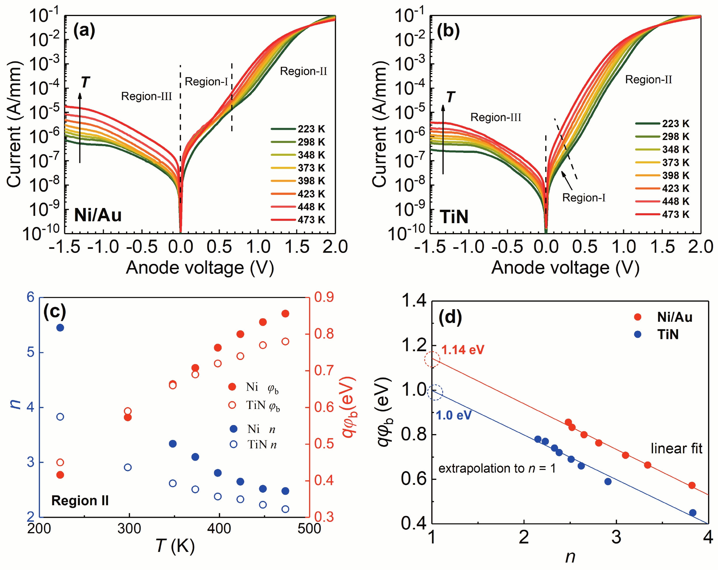
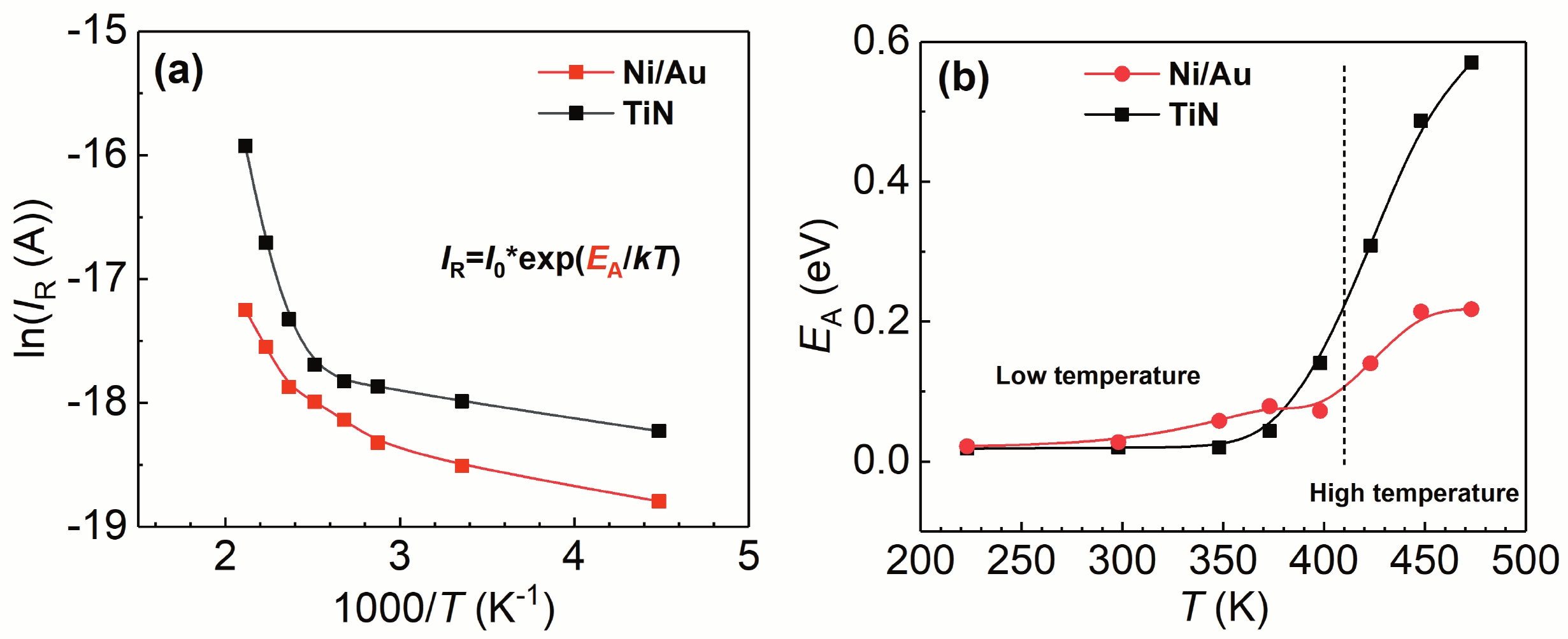
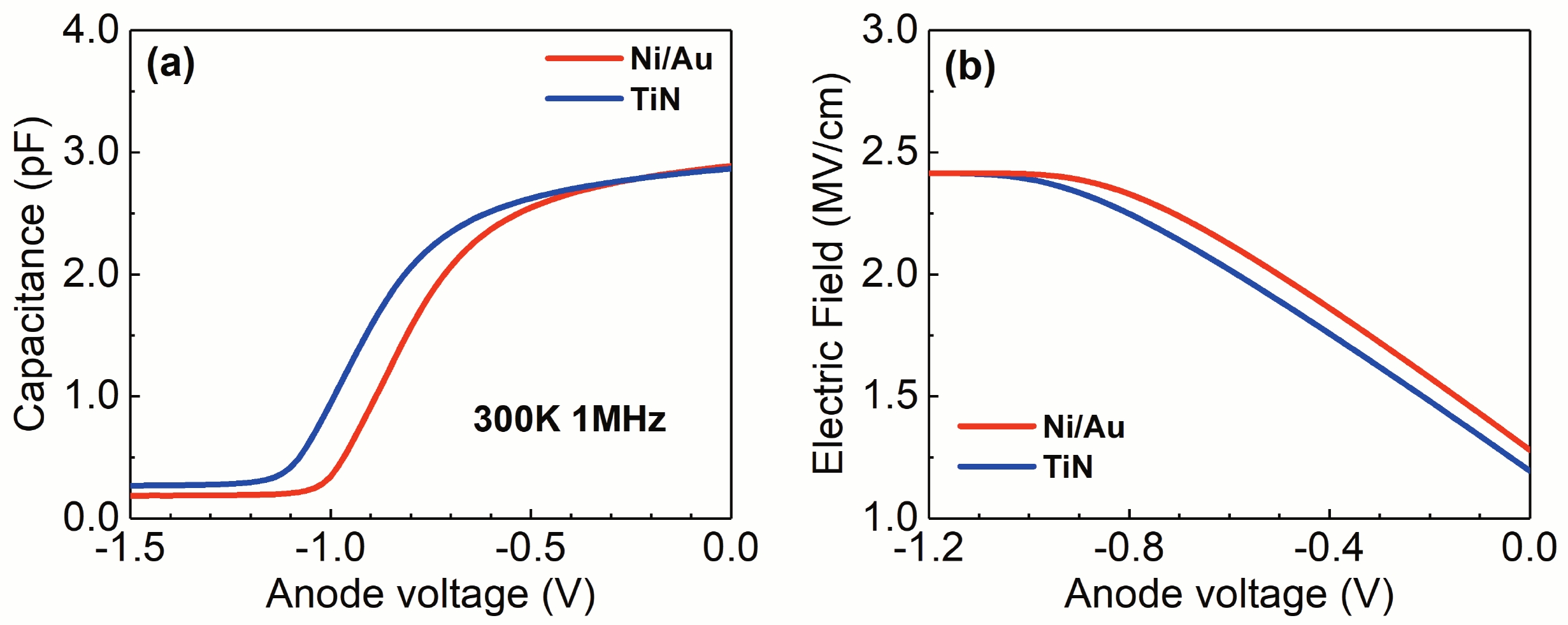
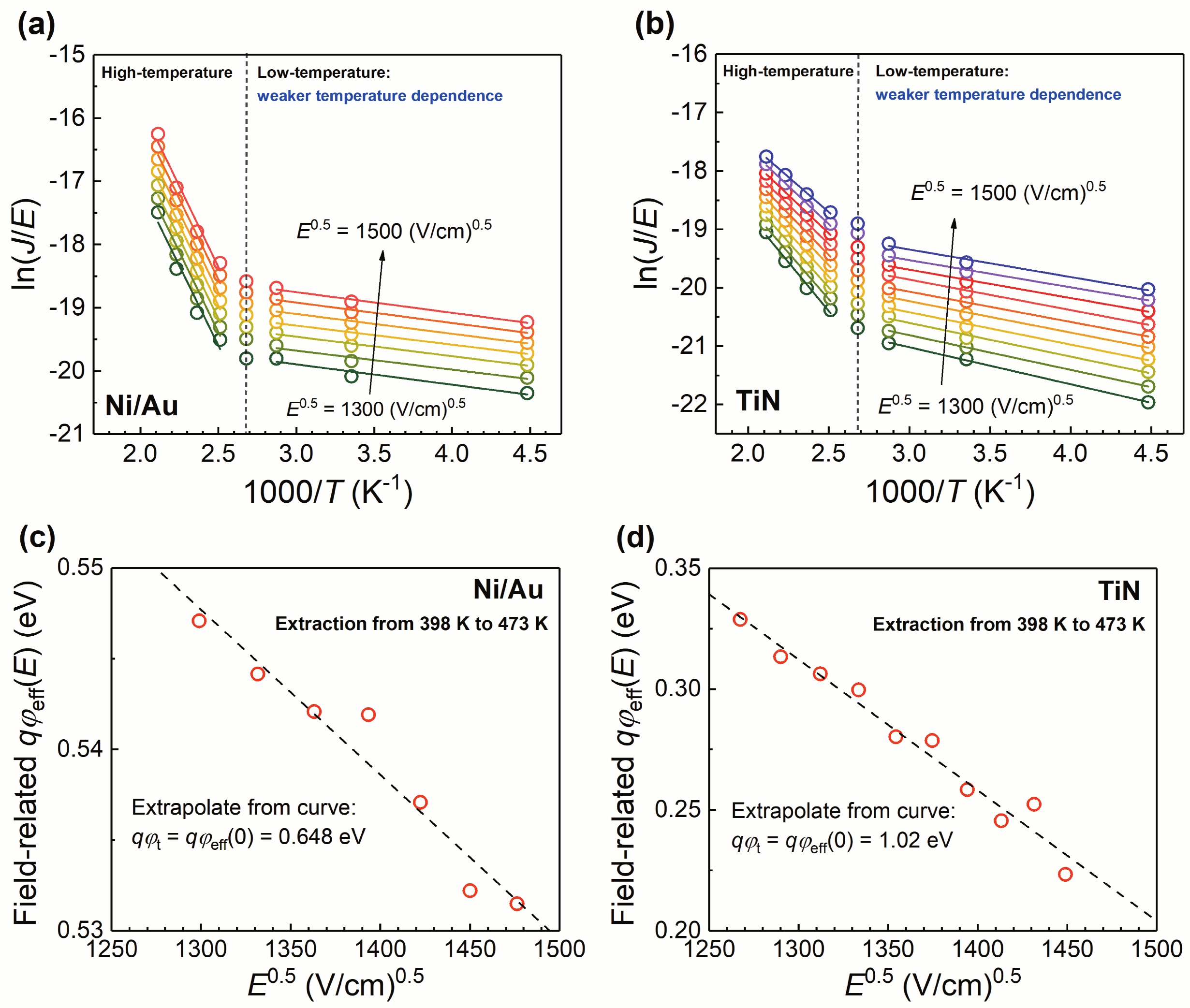
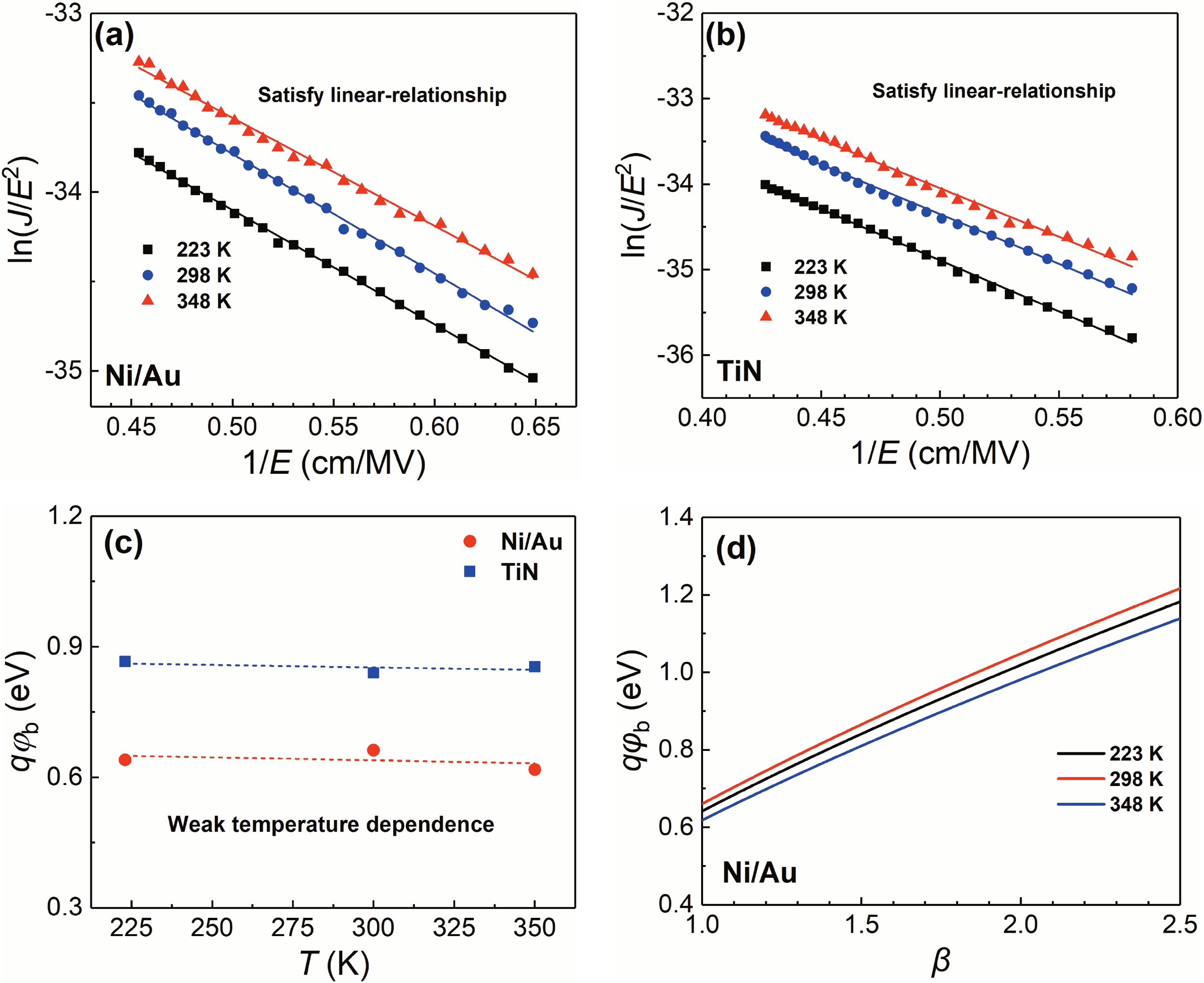
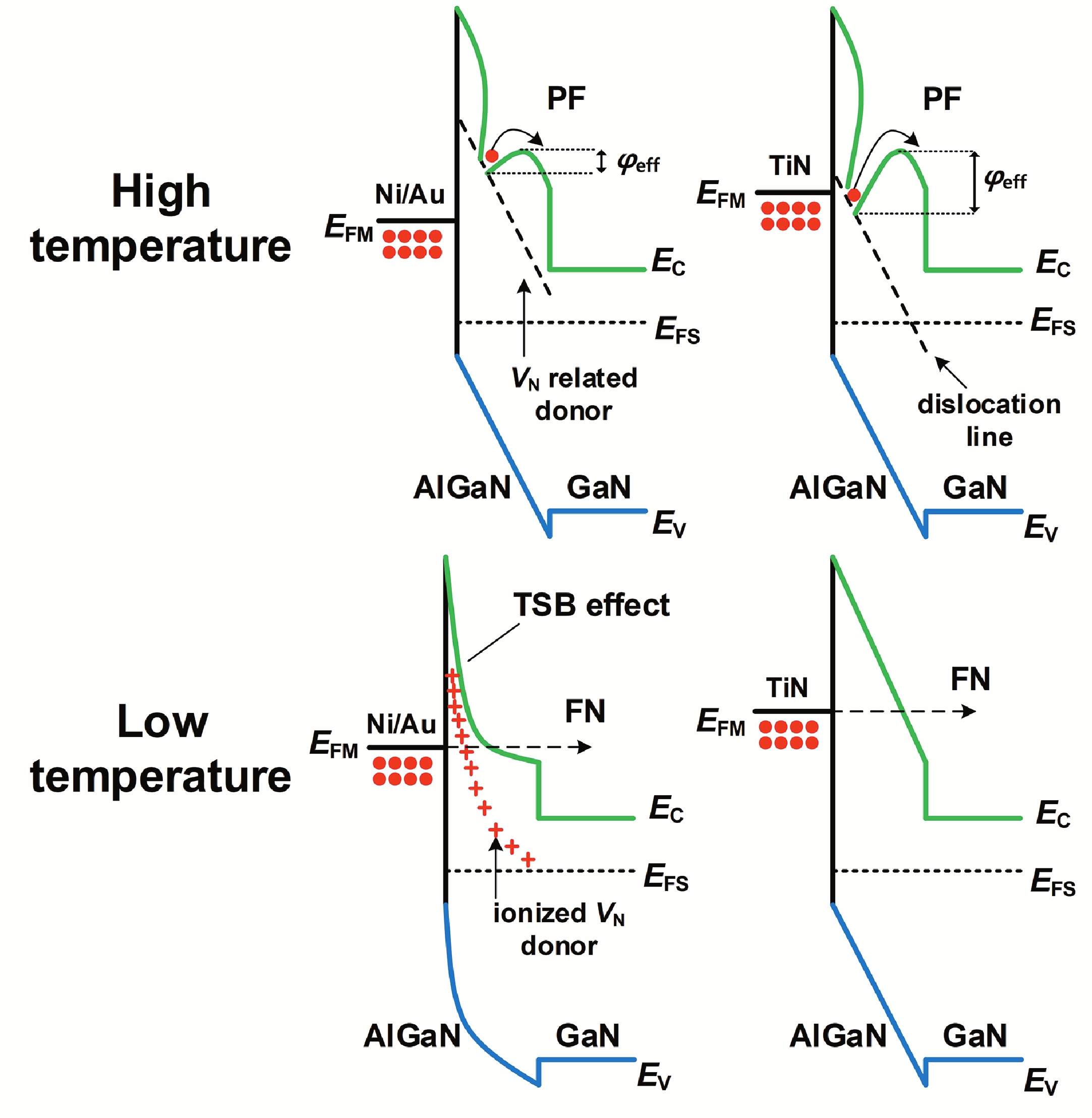
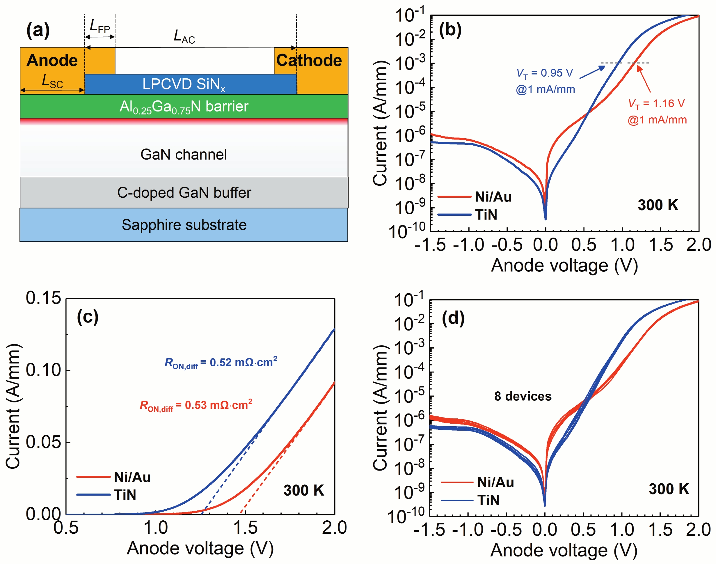
In this work, the optimization of reverse leakage current (IR) and turn-on voltage (VT) in recess-free AlGaN/GaN Schottky barrier diodes (SBDs) was achieved by substituting the Ni/Au anode with TiN anode. To explain this phenomenon, the current transport mechanism was investigated by temperature-dependent current–voltage (I–V) characteristics. For forward bias, the current is dominated by the thermionic emission (TE) mechanisms for both devices. Besides, the presence of inhomogeneity of the Schottky barrier height (qφb) is proved by the linear relationship between qφb and ideality factor. For reverse bias, the current is dominated by two different mechanisms at high temperature and low temperature, respectively. At high temperatures, the Poole–Frenkel emission (PFE) induced by nitrogen-vacancy (VN) is responsible for the high IR in Ni/Au anode. For TiN anode, the IR is dominated by the PFE from threading dislocation (TD), which can be attributed to the decrease of VN due to the suppression of N diffusion at the interface of Schottky contact. At low temperatures, the IR of both diodes is dominated by Fowler–Nordheim (FN) tunneling. However, the VN donor enhances the electric field in the barrier layer, thus causing a higher IR in Ni/Au anode than TiN anode, as confirmed by the modified FN model.-
Keywords:
- AlGaN/GaN,
- Schottky barrier diode,
- TiN,
- current transport mechanism
-
References
[1] Chen K J, Häberlen O, Lidow A, et al. GaN-on-Si power technology: Devices and applications. IEEE Trans Electron Devices, 2017, 64, 779 doi: 10.1109/TED.2017.2657579[2] Eblabla A, Li X, Alathbah M, et al. Multi-channel AlGaN/GaN lateral Schottky barrier diodes on low-resistivity silicon for sub-THz integrated circuits applications. IEEE Electron Device Lett, 2019, 40, 878 doi: 10.1109/LED.2019.2912910[3] Nela L, Kampitsis G, Ma J, et al. Fast-switching tri-anode Schottky barrier diodes for monolithically integrated GaN-on-Si power circuits. IEEE Electron Device Lett, 2020, 41, 99 doi: 10.1109/LED.2019.2957700[4] Xiao M, Ma Y W, Cheng K, et al. 3.3 kV multi-channel AlGaN/GaN Schottky barrier diodes with P-GaN termination. IEEE Electron Device Lett, 2020, 41, 1177 doi: 10.1109/LED.2020.3005934[5] Han S W, Song J N, Yoo S H, et al. Experimental demonstration of charge- balanced GaN super-heterojunction Schottky barrier diode capable of 2.8 kV switching. IEEE Electron Device Lett, 2020, 41, 1758 doi: 10.1109/LED.2020.3029619[6] Dang K, Zhang J C, Zhou H, et al. Lateral GaN Schottky barrier diode for wireless high-power transfer application with high RF/DC conversion efficiency: From circuit construction and device technologies to system demonstration. IEEE Trans Ind Electron, 2020, 67, 6597 doi: 10.1109/TIE.2019.2939968[7] Dang K, Zhang J C, Zhou H, et al. A 5.8-GHz high-power and high-efficiency rectifier circuit with lateral GaN Schottky diode for wireless power transfer. IEEE Trans Power Electron, 2020, 35, 2247 doi: 10.1109/TPEL.2019.2938769[8] Lenci S, de Jaeger B, Carbonell L, et al. Au-free AlGaN/GaN power diode on 8-in Si substrate with gated edge termination. IEEE Electron Device Lett, 2013, 34, 1035 doi: 10.1109/LED.2013.2267933[9] Hu J, Stoffels S, Lenci S, et al. Performance optimization of Au-free lateral AlGaN/GaN Schottky barrier diode with gated edge termination on 200-mm silicon substrate. IEEE Trans Electron Devices, 2016, 63, 997 doi: 10.1109/TED.2016.2515566[10] Biscarrat J, Gwoziecki R, Baines Y, et al. Performance enhancement of CMOS compatible 600V rated AlGaN/GaN Schottky diodes on 200mm silicon wafers. 2018 IEEE 30th International Symposium on Power Semiconductor Devices and ICs, 2018, 200 doi: 10.1109/ISPSD.2018.8393637[11] Li Y, Ng G I, Arulkumaran S, et al. AlGaN/GaN high electron mobility transistors on Si with sputtered TiN gate. Phys Status Solidi A, 2017, 214, 1600555 doi: 10.1002/pssa.201600555[12] Kawanago T, Kakushima K, Kataoka Y, et al. Gate technology contributions to collapse of drain current in AlGaN/GaN Schottky HEMT. IEEE Trans Electron Devices, 2014, 61, 785 doi: 10.1109/TED.2014.2299556[13] Li L A, Nakamura R, Wang Q P, et al. Synthesis of titanium nitride for self-aligned gate AlGaN/GaN heterostructure field-effect transistors. Nanoscale Res Lett, 2014, 9, 590 doi: 10.1186/1556-276X-9-590[14] Kim H, Schuette M, Jung H, et al. Passivation effects in Ni/AlGaN/GaN Schottky diodes by annealing. Appl Phys Lett, 2006, 89, 053516 doi: 10.1063/1.2234569[15] Wu H, Kang X W, Zheng Y K, et al. Analysis of reverse leakage mechanism in recess-free thin-barrier AlGaN/GaN Schottky barrier diode. Jpn J Appl Phys, 2021, 60, 024002 doi: 10.35848/1347-4065/abd86f[16] Kang X W, Wang X H, Huang S, et al. Recess-free AlGaN/GaN lateral Schottky barrier controlled Schottky rectifier with low turn-on voltage and high reverse blocking. 2018 IEEE 30th International Symposium on Power Semiconductor Devices and ICs, 2018, 280 doi: 10.1109/ISPSD.2018.8393657[17] Kang X W, Zheng Y K, Wu H, et al. Thin-barrier gated-edge termination AlGaN/GaN Schottky barrier diode with low reverse leakage and high turn-on uniformity. Semicond Sci Technol, 2021, 36, 094001 doi: 10.1088/1361-6641/ac0b93[18] Sjoblom G, Westlinder J, Olsson J. Investigation of the thermal stability of reactively sputter-deposited TiN MOS gate electrodes. IEEE Trans Electron Devices, 2005, 52, 2349 doi: 10.1109/TED.2005.856796[19] Sathaiya D M, Karmalkar S. Edge effects on gate tunneling current in HEMTs. IEEE Trans Electron Devices, 2007, 54, 2614 doi: 10.1109/TED.2007.904993[20] Saadaoui S, Mongi Ben Salem M, Gassoumi M, et al. Electrical characterization of (Ni/Au)/Al0.25Ga0.75N/GaN/SiC Schottky barrier diode. J Appl Phys, 2011, 110, 013701 doi: 10.1063/1.3600229[21] Arehart A R, Moran B, Speck J S, et al. Effect of threading dislocation density on Ni/n-GaN Schottky diode I-V characteristics. J Appl Phys, 2006, 100, 023709 doi: 10.1063/1.2219985[22] Kim H, Song K M. Dislocation-related electron transport in Au Schottky junctions on AlGaN/GaN. Trans Electr Electron Mater, 2018, 19, 101 doi: 10.1007/s42341-018-0015-y[23] Chatterjee A, Khamari S K, Dixit V K, et al. Dislocation-assisted tunnelling of charge carriers across the Schottky barrier on the hydride vapour phase epitaxy grown GaN. J Appl Phys, 2015, 118, 175703 doi: 10.1063/1.4934862[24] Peta K R, Park B G, Lee S T, et al. Analysis of electrical properties and deep level defects in undoped GaN Schottky barrier diode. Thin Solid Films, 2013, 534, 603 doi: 10.1016/j.tsf.2013.01.100[25] Tung R T. Electron transport at metal-semiconductor interfaces: General theory. Phys Rev B, 1992, 45, 13509 doi: 10.1103/PhysRevB.45.13509[26] Schmitsdorf R F. Explanation of the linear correlation between barrier heights and ideality factors of real metal-semiconductor contacts by laterally nonuniform Schottky barriers. J Vac Sci Technol B, 1997, 15, 1221 doi: 10.1116/1.589442[27] Qiao D, Yu L S, Lau S S, et al. Dependence of Ni/AlGaN Schottky barrier height on Al mole fraction. J Appl Phys, 1999, 87, 801 doi: 10.1063/1.371944[28] Yan D W, Lu H, Cao D S, et al. On the reverse gate leakage current of AlGaN/GaN high electron mobility transistors. Appl Phys Lett, 2010, 97, 153503 doi: 10.1063/1.3499364[29] Ambacher O, Smart J, Shealy J R, et al. Two-dimensional electron gases induced by spontaneous and piezoelectric polarization charges in N- and Ga-face AlGaN/GaN heterostructures. J Appl Phys, 1999, 85, 3222 doi: 10.1063/1.369664[30] Mahaveer Sathaiya D, Karmalkar S. Thermionic trap-assisted tunneling model and its application to leakage current in nitrided oxides and AlGaN∕GaN high electron mobility transistors. J Appl Phys, 2006, 99, 093701 doi: 10.1063/1.2191620[31] Yeargan J R, Taylor H L. The Poole-Frenkel effect with compensation present. J Appl Phys, 1968, 39, 5600 doi: 10.1063/1.1656022[32] Zhang H, Miller E J, Yu E T. Analysis of leakage current mechanisms in Schottky contacts to GaN and Al0.25Ga0.75N∕GaN grown by molecular-beam epitaxy. J Appl Phys, 2006, 99, 023703 doi: 10.1063/1.2159547[33] Fang Z Q, Farlow G C, Claflin B, et al. Effects of electron-irradiation on electrical properties of AlGaN/GaN Schottky barrier diodes. J Appl Phys, 2009, 105, 123704 doi: 10.1063/1.3151952[34] Fang Z Q, Look D C, Kim D H, et al. Traps in AlGaN/GaN/SiC heterostructures studied by deep level transient spectroscopy. Appl Phys Lett, 2005, 87, 182115 doi: 10.1063/1.2126145[35] Katsuno T, Kanechika M, Itoh K, et al. Improvement of current collapse by surface treatment and passivation layer in p-GaN gate GaN high-electron-mobility transistors. Jpn J Appl Phys, 2013, 52, 04CF08 doi: 10.7567/JJAP.52.04CF08[36] Johnstonea D K, Ahoujjab M, Yeoc Y K, et al. Deep centers and their capture barriers in MOCVD-grown GaN. MRS Proc, 2001, 692, H2.7.1 doi: 10.1557/PROC-692-H2.7.1[37] Whiting P G, Holzworth M R, Lind A G, et al. Erosion defect formation in Ni-gate AlGaN/GaN high electron mobility transistors. Microelectron Reliab, 2017, 70, 32 doi: 10.1016/j.microrel.2017.01.007[38] Koehler A D, Nepal N, Anderson T J, et al. Atomic layer epitaxy AlN for enhanced AlGaN/GaN HEMT passivation. IEEE Electron Device Lett, 2013, 34, 1115 doi: 10.1109/LED.2013.2274429[39] Xu Y N, Ching W Y. Electronic, optical, and structural properties of some wurtzite crystals. Phys Rev B, 1993, 48, 4335 doi: 10.1103/PhysRevB.48.4335[40] Hasegawa H, Inagaki T, Ootomo S, et al. Mechanisms of current collapse and gate leakage currents in AlGaN/GaN heterostructure field effect transistors. J Vac Sci Technol B, 2003, 21, 1844 doi: 10.1116/1.1589520 -
Proportional views


 DownLoad:
