REVIEWS

Review in situ transmission electron microscope with machine learning

Zhiheng Cheng, Chaolun Wang, Xing Wu and Junhao Chu

+ Author Affiliations

 Corresponding author: Chaolun Wang, clwang@cee.ecnu.edu.cn; Xing Wu, xwu@cee.ecnu.edu.cn

PDF

Turn off MathJax

Abstract: Advanced electronic materials are the fundamental building blocks of integrated circuits (ICs). The microscale properties of electronic materials (e.g., crystal structures, defects, and chemical properties) can have a considerable impact on the performance of ICs. Comprehensive characterization and analysis of the material in real time with high-spatial resolution are indispensable. In situ transmission electron microscope (TEM) with atomic resolution and external field can be applied as a physical simulation platform to study the evolution of electronic material in working conditions. The high-speed camera of the in situ TEM generates a high frame rate video, resulting in a large dataset that is beyond the data processing ability of researchers using the traditional method. To overcome this challenge, many works on automated TEM analysis by using machine-learning algorithm have been proposed. In this review, we introduce the technical evolution of TEM data acquisition, including analysis, and we summarize the application of machine learning to TEM data analysis in the aspects of morphology, defect, structure, and spectra. Some of the challenges of automated TEM analysis are given in the conclusion.

Key words: electron microscopymachine learningin situimage analysissemiconductor


[1]
Avsar A, Ciarrocchi A, Pizzochero M, et al. Defect induced, layer-modulated magnetism in ultrathin metallic PtSe2. Nat Nanotechnol, 2019, 14, 674 doi: 10.1038/s41565-019-0467-1
[2]
Zhou M, Wang W, Lu J, et al. How defects influence the photoluminescence of TMDCs. Nano Res, 2021, 14, 29 doi: 10.1007/s12274-020-3037-9
[3]
Jiang J, Ni Z. Defect engineering in two-dimensional materials. J Semicond, 2019, 40, 070403 doi: 10.1088/1674-4926/40/7/070403
[4]
Chen X, Du F, Wang C, et al. Direct visualization of breakdown-induced metal migration in enhanced modified lateral silicon-controlled rectifiers. IEEE Trans Electron Devices, 2021, 68, 1378 doi: 10.1109/TED.2021.3053501
[5]
Wu X, Luo C, Hao P, et al. Probing and manipulating the interfacial defects of InGaAs dual-layer metal oxides at the atomic scale. Adv Mater, 2018, 30, 1703025 doi: 10.1002/adma.201703025
[6]
Luo C, Wang C, Wu X, et al. In situ transmission electron microscopy characterization and manipulation of two-dimensional layered materials beyond graphene. Small, 2017, 13, 1604259 doi: 10.1002/smll.201604259
[7]
Mendes R G, Pang J, Bachmatiuk A, et al. Electron-driven in situ transmission electron microscopy of 2D transition metal dichalcogenides and their 2D heterostructures. ACS Nano, 2019, 13, 978 doi: 10.1021/acsnano.8b08079
[8]
Dong Z, Ma Y. Atomic-level handedness determination of chiral crystals using aberration-corrected scanning transmission electron microscopy. Nat Commun, 2020, 11, 1588 doi: 10.1038/s41467-020-15388-5
[9]
Zaluzec N J. The influence of Cs/Cc correction in analytical imaging and spectroscopy in scanning and transmission electron microscopy. Ultramicroscopy, 2015, 151, 240 doi: 10.1016/j.ultramic.2014.09.012
[10]
Lin Y, Zhou M, Tai X, et al. Analytical transmission electron microscopy for emerging advanced materials. Matter, 2021, 4, 2309 doi: 10.1016/j.matt.2021.05.005
[11]
Zhang J, Yu Y, Wang P, et al. Characterization of atomic defects on the photoluminescence in two-dimensional materials using transmission electron microscope. InfoMat, 2019, 1, 85 doi: 10.1002/inf2.12002
[12]
Kim B H, Yang J, Lee D, et al. Liquid-phase transmission electron microscopy for studying colloidal inorganic nanoparticles. Adv Mater, 2018, 30, 1703316 doi: 10.1002/adma.201703316
[13]
Fan Z, Zhang L, Baumann D, et al. In situ transmission electron microscopy for energy materials and devices. Adv Mater, 2019, 31, 1900608 doi: 10.1002/adma.201900608
[14]
Yang X, Luo C, Tian X Y, et al. A review of in situ transmission electron microscopy study on the switching mechanism and packaging reliability in non-volatile memory. J Semicond, 2021, 42, 013102 doi: 10.1088/1674-4926/42/1/013102
[15]
Zhang C, Larionov K V, Firestein K L, et al. Optomechanical properties of MoSe2 nanosheets as revealed by in situ transmission electron microscopy. Nano Lett, 2022, 22, 673 doi: 10.1021/acs.nanolett.1c03796
[16]
de Jonge N, Houben L, Dunin-Borkowski R E, et al. Resolution and aberration correction in liquid cell transmission electron microscopy. Nat Rev Mater, 2019, 4, 61 doi: 10.1038/s41578-018-0071-2
[17]
Xu H, Wu X, Tian X, et al. Dynamic structure-properties characterization and manipulation in advanced nanodevices. Mater Today Nano, 2019, 7, 100042 doi: 10.1016/j.mtnano.2019.100042
[18]
Cai J S, Cai R, Sun Z T, et al. Confining TiO2 nanotubes in PECVD-enabled graphene capsules toward ultrafast K-ion storage: in situ TEM/XRD study and DFT analysis. Nano-Micro Lett, 2020, 12, 123 doi: 10.1007/s40820-020-00460-y
[19]
Wang R B, Song Z T, Song W X, et al. Phase-change memory based on matched Ge-Te, Sb-Te, and In-Te octahedrons: Improved electrical performances and robust thermal stability. Infomat, 2021, 3, 1008 doi: 10.1002/inf2.12233
[20]
Wang Y H, Pang J B, Cheng Q L, et al. Applications of 2D-layered palladium diselenide and its van der Waals heterostructures in electronics and optoelectronics. Nano-Micro Lett, 2021, 13, 143 doi: 10.1007/s40820-021-00660-0
[21]
Wu Y L, Gaddam R R, Zhang C, et al. Stabilising cobalt sulphide nanocapsules with nitrogen-doped carbon for high-performance sodium-ion storage. Nano-Micro Lett, 2020, 12, 48 doi: 10.1007/s40820-020-0391-9
[22]
Zhang H, Yang Y, Xu H, et al. Li4Ti5O12 spinel anode: Fundamentals and advances in rechargeable batteries. Infomat, 2021, 4, e12228 doi: 10.1002/inf2.12228
[23]
Ibrahim I, Kalbacova J, Engemaier V, et al. Confirming the dual role of etchants during the enrichment of semiconducting single wall carbon nanotubes by chemical vapor deposition. Chem Mater, 2015, 27, 5964 doi: 10.1021/acs.chemmater.5b02037
[24]
Pang J, Wang Y, Yang X, et al. A wafer-scale two-dimensional platinum monosulfide ultrathin film via metal sulfurization for high performance photoelectronics. Mater Adv, 2022, 3, 1497 doi: 10.1039/D1MA00757B
[25]
Sun Y, Sun B, He J B, et al. Compositional and structural engineering of inorganic nanowires toward advanced properties and applications. Infomat, 2019, 1, 496 doi: 10.1002/inf2.12049
[26]
Wang J W, Jia Z R, Liu X H, et al. Construction of 1D heterostructure NiCo@C/ZnO nanorod with enhanced microwave absorption. Nano-Micro Lett, 2021, 13, 175 doi: 10.1007/s40820-021-00704-5
[27]
Yu B J, Liu S D, Xie W H, et al. Versatile core-shell magnetic fluorescent mesoporous microspheres for multilevel latent fingerprints magneto-optic information recognition. Infomat, 2022, 4, e12289 doi: 10.1002/inf2.12289
[28]
Schorb M, Haberbosch I, Hagen W J H, et al. Software tools for automated transmission electron microscopy. Nat Methods, 2019, 16, 471 doi: 10.1038/s41592-019-0396-9
[29]
Plotkin-Swing B, Corbin G J, De Carlo S, et al. Hybrid pixel direct detector for electron energy loss spectroscopy. Ultramicroscopy, 2020, 217, 113067 doi: 10.1016/j.ultramic.2020.113067
[30]
Maigné A, Wolf M. Low-dose electron energy-loss spectroscopy using electron counting direct detectors. Microscopy, 2018, 67, i86 doi: 10.1093/jmicro/dfx088
[31]
Chen X, Zhou L H, Wang P, et al. Effects associated with nanostructure fabrication using in situ liquid cell TEM technology. Nano-Micro Lett, 2015, 7, 385 doi: 10.1007/s40820-015-0054-4
[32]
Zhang S, Pang J B, Cheng Q L, et al. High-performance electronics and optoelectronics of monolayer tungsten diselenide full film from pre-seeding strategy. Infomat, 2021, 3, 1455 doi: 10.1002/inf2.12259
[33]
Ishida T, Shinozaki A, Kuwahara M, et al. Performance of a silicon-on-insulator direct electron detector in a low-voltage transmission electron microscope. Microscopy, 2021, 70, 321 doi: 10.1093/jmicro/dfaa072
[34]
Ophus C, Ciston J, Pierce J, et al. Efficient linear phase contrast in scanning transmission electron microscopy with matched illumination and detector interferometry. Nat Commun, 2016, 7, 10719 doi: 10.1038/ncomms10719
[35]
Hui F, Li C, Chen Y H, et al. Understanding the structural evolution of Au/WO2.7 compounds in hydrogen atmosphere by atomic scale in situ environmental TEM. Nano Res, 2020, 13, 3019 doi: 10.1007/s12274-020-2966-7
[36]
Jiang Y, Zhang Z F, Yuan W T, et al. Recent advances in gas-involved in situ studies via transmission electron microscopy. Nano Res, 2018, 11, 42 doi: 10.1007/s12274-017-1645-9
[37]
Wang Y, Peng X X, Abelson A, et al. In situ TEM observation of neck formation during oriented attachment of PbSe nanocrystals. Nano Res, 2019, 12, 2549 doi: 10.1007/s12274-019-2483-8
[38]
Weng B, Jiang Y H, Liao H G, et al. Visualizing light-induced dynamic structural transformations of Au clusters-based photocatalyst via in situ TEM. Nano Res, 2021, 14, 2805 doi: 10.1007/s12274-021-3289-z
[39]
Zhu Y T, Yuan D D, Zhang H, et al. Atomic-scale insights into the formation of 2D crystals from in situ transmission electron microscopy. Nano Res, 2021, 14, 1650 doi: 10.1007/s12274-020-3034-z
[40]
Alberti A, Bongiorno C, Smecca E, et al. Pb clustering and PbI2 nanofragmentation during methylammonium lead iodide perovskite degradation. Nat Commun, 2019, 10, 2196 doi: 10.1038/s41467-019-09909-0
[41]
Spurgeon S R, Ophus C, Jones L, et al. Towards data-driven next-generation transmission electron microscopy. Nat Mater, 2020, 20, 274 doi: 10.1038/s41563-020-00833-z
[42]
Kalinin S V, Lupini A R, Dyck O, et al. Lab on a beam—Big data and artificial intelligence in scanning transmission electron microscopy. MRS Bull, 2019, 44, 565 doi: 10.1557/mrs.2019.159
[43]
Uesugi F, Koshiya S, Kikkawa J, et al. Non-negative matrix factorization for mining big data obtained using four-dimensional scanning transmission electron microscopy. Ultramicroscopy, 2021, 221, 113168 doi: 10.1016/j.ultramic.2020.113168
[44]
Dyck O, Ziatdinov M, Lingerfelt D B, et al. Atom-by-atom fabrication with electron beams. Nat Rev Mater, 2019, 4, 497 doi: 10.1038/s41578-019-0118-z
[45]
Chen M, Dai W, Sun S Y, et al. Convolutional neural networks for automated annotation of cellular cryo-electron tomograms. Nat Methods, 2017, 14, 983 doi: 10.1038/nmeth.4405
[46]
Lee C H, Khan A, Luo D, et al. Deep learning enabled strain mapping of single-atom defects in two-dimensional transition metal dichalcogenides with sub-picometer precision. Nano Lett, 2020, 20, 3369 doi: 10.1021/acs.nanolett.0c00269
[47]
Vasudevan R K, Ziatdinov M, Jesse S, et al. Phases and interfaces from real space atomically resolved data: physics-based deep data image analysis. Nano Lett, 2016, 16, 5574 doi: 10.1021/acs.nanolett.6b02130
[48]
Belianinov A, He Q, Kravchenko M, et al. Identification of phases, symmetries and defects through local crystallography. Nat Commun, 2015, 6, 7801 doi: 10.1038/ncomms8801
[49]
Nelson C T, Vasudevan R K, Zhang X, et al. Exploring physics of ferroelectric domain walls via Bayesian analysis of atomically resolved STEM data. Nat Commun, 2020, 11, 6361 doi: 10.1038/s41467-020-19907-2
[50]
LeCun Y, Boser B, Denker J S, et al. Backpropagation applied to handwritten zip code recognition. Neural Comput, 1989, 1, 541 doi: 10.1162/neco.1989.1.4.541
[51]
Krizhevsky A, Sutskever I, Hinton G E. ImageNet classification with deep convolutional neural networks. Proceedings of the 25th International Conference on Neural Information Processing Systems - Volume 1, 2012, 1097
[52]
Ronneberger O, Fischer P, Brox T. U-Net: convolutional networks for biomedical image segmentation. Medical Image Computng and Computer-Assisted Intervention – MICCAI 2015, Springer International Publishing, 2015, 234
[53]
LeCun Y, Bengio Y, Hinton G. Deep learning. Nature, 2015, 521, 436 doi: 10.1038/nature14539
[54]
Chen L C, Zhu Y, Papandreou G, et al. Encoder-decoder with atrous separable convolution for semantic image segmentation. Proceedings of the 15th European Conference on Computer Vision (ECCV), 2018
[55]
Ge M, Su F, Zhao Z, et al. Deep learning analysis on microscopic imaging in materials science. Mater Today Nano, 2020, 11, 100087 doi: 10.1016/j.mtnano.2020.100087
[56]
Dan J, Zhao X, Pennycook S J. A machine perspective of atomic defects in scanning transmission electron microscopy. InfoMat, 2019, 1, 359 doi: 10.1002/inf2.12026
[57]
Li W, Field K G, Morgan D. Automated defect analysis in electron microscopic images. npj Comput Mater, 2018, 4, 36 doi: 10.1038/s41524-018-0093-8
[58]
Maksov A, Dyck O, Wang K, et al. Deep learning analysis of defect and phase evolution during electron beam-induced transformations in WS2. npj Comput Mater, 2019, 5, 12 doi: 10.1038/s41524-019-0152-9
[59]
Ede J M, Beanland R. Partial scanning transmission electron microscopy with deep learning. Sci Rep, 2020, 10, 8332 doi: 10.1038/s41598-020-65261-0
[60]
Zhang C, Feng J, DaCosta L R, et al. Atomic resolution convergent beam electron diffraction analysis using convolutional neural networks. Ultramicroscopy, 2019, 210, 112921 doi: 10.1017/S1431927619001375
[61]
Wang C, Zou Q, Cheng Z, et al. Tailoring atomic 1T phase CrTe2 for in situ fabrication. Nanotechnology, 2021, 33, 085302 doi: 10.1088/1361-6528/ac3a3a
[62]
Ziletti A, Kumar D, Scheffler M, et al. Insightful classification of crystal structures using deep learning. Nat Commun, 2018, 9, 2775 doi: 10.1038/s41467-018-05169-6
[63]
Yao L, Ou Z, Luo B, et al. Machine learning to reveal nanoparticle dynamics from liquid-phase TEM videos. ACS Cent Sci, 2020, 6, 1421 doi: 10.1021/acscentsci.0c00430
[64]
Yang S H, Choi W, Cho B W, et al. Deep learning-assisted quantification of atomic dopants and defects in 2D materials. Adv Sci, 2021, 8, 2101099 doi: 10.1002/advs.202101099
[65]
Roccapriore K M, Ziatdinov M, Cho S H, et al. Predictability of localized plasmonic responses in nanoparticle assemblies. Small, 2021, 17, 2100181 doi: 10.1002/smll.202100181
[66]
Kalinin S V, Dyck O, Jesse S, et al. Exploring order parameters and dynamic processes in disordered systems via variational autoencoders. Sci Adv, 2021, 7, eabd5084 doi: 10.1126/sciadv.abd5084
[67]
Han Y, Jang J, Cha E, et al. Deep learning STEM-EDX tomography of nanocrystals. Nat Mach Intell, 2021, 3, 267 doi: 10.1038/s42256-020-00289-5
[68]
Wang X, Li J, Ha H D, et al. Autodetect-mNP: an unsupervised machine learning algorithm for automated analysis of transmission electron microscope images of metal nanoparticles. J Am Chem Soc, 2021, 1, 316 doi: 10.1021/jacsau.0c00030
[69]
Ragone M, Yurkiv V, Song B, et al. Atomic column heights detection in metallic nanoparticles using deep convolutional learning. Comput Mater Sci, 2020, 180, 109722 doi: 10.1016/j.commatsci.2020.109722
[70]
Lee B, Yoon S, Lee J W, et al. Statistical characterization of the morphologies of nanoparticles through machine learning based electron microscopy image analysis. ACS Nano, 2020, 14, 17125 doi: 10.1021/acsnano.0c06809
[71]
Förster G D, Castan A, Loiseau A, et al. A deep learning approach for determining the chiral indices of carbon nanotubes from high-resolution transmission electron microscopy images. Carbon, 2020, 169, 465 doi: 10.1016/j.carbon.2020.06.086
[72]
Ziatdinov M, Dyck O, Maksov A, et al. Deep learning of atomically resolved scanning transmission electron microscopy images: Chemical identification and tracking local transformations. ACS Nano, 2017, 11, 12742 doi: 10.1021/acsnano.7b07504
[73]
Li W S, Ning H K, Yu Z H, et al. Reducing the power consumption of two-dimensional logic transistors. J Semicond, 2019, 40, 091002 doi: 10.1088/1674-4926/40/9/091002
[74]
Wang J L. A novel spin-FET based on 2D antiferromagnet. J Semicond, 2019, 40, 020401 doi: 10.1088/1674-4926/40/2/020401
[75]
Liang F, Wang C, Luo C, et al. Ferromagnetic CoSe broadband photodetector at room temperature. Nanotechnology, 2020, 31, 374002 doi: 10.1088/1361-6528/ab9867
[76]
Zhang H, Jiang X T, Wang Y L, et al. Preface to the special issue on monoelemental 2D semiconducting materials and their applications. J Semicond, 2020, 41, 080101 doi: 10.1088/1674-4926/41/8/080101
[77]
Zhou J S, Yang J H, Wei Z M. Photodetectors based on 2D material/Si heterostructure. J Semicond, 2020, 41, 080401 doi: 10.1088/1674-4926/41/8/080401
[78]
Deng N Q, Tian H, Zhang J, et al. Black phosphorus junctions and their electrical and optoelectronic applications. J Semicond, 2021, 42, 081001 doi: 10.1088/1674-4926/42/8/081001
[79]
Wang C L, Wu X, Ma Y H, et al. Metallic few-layered VSe2 nanosheets: high two-dimensional conductivity for flexible in-plane solid-state supercapacitors. J Mater Chem A, 2018, 6, 8299 doi: 10.1039/C8TA00089A
[80]
Wang C, Wu X, Zhang X, et al. Iron-doped VSe2 nanosheets for enhanced hydrogen evolution reaction. Appl Phys Lett, 2020, 116, 223901 doi: 10.1063/5.0008092
[81]
Qiu H, Xu T, Wang Z, et al. Hopping transport through defect-induced localized states in molybdenum disulphide. Nat Commun, 2013, 4, 2642 doi: 10.1038/ncomms3642
[82]
Wang C, Jin M, Liu D, et al. VSe2 quantum dots with high-density active edges for flexible efficient hydrogen evolution reaction. J Phys D, 2021, 54, 214006 doi: 10.1088/1361-6463/abe78d
[83]
Zhang S, Wang C G, Li M Y, et al. Defect structure of localized excitons in a WSe2 monolayer. Phys Rev Lett, 2017, 119, 046101 doi: 10.1103/PhysRevLett.119.046101
[84]
Wang X, Zhang Y, Si H, et al. Single-atom vacancy defect to trigger high-efficiency hydrogen evolution of MoS2. J Am Chem Soc, 2020, 142, 4298 doi: 10.1021/jacs.9b12113
[85]
Barthelmi K, Klein J, Hötger A, et al. Atomistic defects as single-photon emitters in atomically thin MoS2. Appl Phys Lett, 2020, 117, 070501 doi: 10.1063/5.0018557
[86]
Susi T, Meyer J C, Kotakoski J. Manipulating low-dimensional materials down to the level of single atoms with electron irradiation. Ultramicroscopy, 2017, 180, 163 doi: 10.1016/j.ultramic.2017.03.005
[87]
Pennycook S J, Jesson D E. High-resolution Z-contrast imaging of crystals. Ultramicroscopy, 1991, 37, 14 doi: 10.1016/0304-3991(91)90004-P
[88]
Boyes E D, LaGrow A P, Ward M R, et al. Single atom dynamics in chemical reactions. Acc Chem Res, 2020, 53, 390 doi: 10.1021/acs.accounts.9b00500
[89]
Mi R, Li D, Hu Z, et al. Morphology effects of CeO2 nanomaterials on the catalytic combustion of toluene: a combined kinetics and diffuse reflectance infrared fourier transform spectroscopy study. ACS Catal, 2021, 11, 7876 doi: 10.1021/acscatal.1c01981
[90]
Ni B, Wang X. Face the edges: catalytic active sites of nanomaterials. Adv Sci, 2015, 2, 1500085 doi: 10.1002/advs.201500085
[91]
Zheng H M. Imaging, understanding, and control of nanoscale materials transformations. MRS Bull, 2021, 46, 443 doi: 10.1557/s43577-021-00113-4
[92]
Wang W H, Chee S W, Yan H W, et al. Growth dynamics of vertical and lateral layered double hydroxide nanosheets during electrodeposition. Nano Lett, 2021, 21, 5977 doi: 10.1021/acs.nanolett.1c00898
[93]
Shi F, Peng J, Li F, et al. Design of highly durable core−shell catalysts by controlling shell distribution guided by in situ corrosion study. Adv Mater, 2021, 33, 2101511 doi: 10.1002/adma.202101511
[94]
Ou Z, Wang Z, Luo B, et al. Kinetic pathways of crystallization at the nanoscale. Nat Mater, 2020, 19, 450 doi: 10.1038/s41563-019-0514-1
[95]
Hauwiller M R, Ye X, Jones M R, et al. Tracking the effects of ligands on oxidative etching of gold nanorods in graphene liquid cell electron microscopy. ACS Nano, 2020, 14, 10239 doi: 10.1021/acsnano.0c03601
[96]
Shan H, Gao W, Xiong Y, et al. Nanoscale kinetics of asymmetrical corrosion in core-shell nanoparticles. Nat Commun, 2018, 9, 1011 doi: 10.1038/s41467-018-03372-z
[97]
Liao H G, Zherebetskyy D, Xin H, et al. Facet development during platinum nanocube growth. Science, 2014, 345, 916 doi: 10.1126/science.1253149
[98]
Wang F K, Yang S J, Zhai T Y. 2D Bi2Se3 materials for optoelectronics. iScience, 2021, 24, 103291 doi: 10.1016/j.isci.2021.103291
[99]
Li Q, Lu J, Gupta P, et al. Engineering optical absorption in graphene and other 2D materials: Advances and applications. Adv Opt Mater, 2019, 7, 1900595 doi: 10.1002/adom.201900595
[100]
Qiao J, Kong X, Hu Z X, et al. High-mobility transport anisotropy and linear dichroism in few-layer black phosphorus. Nat Commun, 2014, 5, 4475 doi: 10.1038/ncomms5475
[101]
O'Leary C M, Allen C S, Huang C, et al. Phase reconstruction using fast binary 4D STEM data. Appl Phys Lett, 2020, 116, 124101 doi: 10.1063/1.5143213
[102]
Flannigan D J, Zewail A H. 4D electron microscopy: principles and applications. Acc Chem Res, 2012, 45, 1828 doi: 10.1021/ar3001684
[103]
Zeltmann S E, Muller A, Bustillo K C, et al. Patterned probes for high precision 4D-STEM bragg measurements. Ultramicroscopy, 2020, 209, 112890 doi: 10.1016/j.ultramic.2019.112890
[104]
Koch C. Determination of core structure periodicity and point defect density along dislocations. PhD Thesis, Arizona State University, 2002
[105]
Su J, Wang M, Li Y, et al. Sub-millimeter-scale monolayer p-type H-phase VS2. Adv Funct Mater, 2020, 16, 2000240 doi: 10.1002/adfm.202000240
[106]
Ji Q, Li C, Wang J, et al. Metallic vanadium disulfide nanosheets as a platform material for multifunctional electrode applications. Nano Lett, 2017, 17, 4908 doi: 10.1021/acs.nanolett.7b01914
[107]
Tao L, Chen K, Chen Z, et al. Centimeter-scale CVD growth of highly crystalline single-layer MoS2 film with spatial homogeneity and the visualization of grain boundaries. ACS Appl Mater Interfaces, 2017, 9, 12073 doi: 10.1021/acsami.7b00420
[108]
Acerce M, Voiry D, Chhowalla M. Metallic 1T phase MoS2 nanosheets as supercapacitor electrode materials. Nat Nanotechnol, 2015, 10, 313 doi: 10.1038/nnano.2015.40
[109]
Teich D, Seifert G, Iijima S, et al. Helicity in ropes of chiral nanotubes: calculations and observation. Phys Rev Lett, 2012, 108, 235501 doi: 10.1103/PhysRevLett.108.235501
[110]
Tang M S Y, Ng E P, Juan J C, et al. Metallic and semiconducting carbon nanotubes separation using an aqueous two-phase separation technique: a review. Nanotechnology, 2016, 27, 332002 doi: 10.1088/0957-4484/27/33/332002
[111]
Warner J H, Lin Y C, He K, et al. Atomic level spatial variations of energy states along graphene edges. Nano Lett, 2014, 14, 6155 doi: 10.1021/nl5023095
[112]
Yin Z W, Zhao W, Li J, et al. Advanced electron energy loss spectroscopy for battery studies. Adv Funct Mater, 2022, 32, 2107190 doi: 10.1002/adfm.202107190
[113]
Pokle A, Coelho J, Macguire E, et al. EELS probing of lithium based 2D battery compounds processed by liquid phase exfoliation. Nano Energy, 2016, 30, 18 doi: 10.1016/j.nanoen.2016.09.021
[114]
Ali H, Maynau C, Lajaunie L, et al. Transmission electron microscopy and electron energy-loss spectroscopy studies of hole-selective molybdenum oxide contacts in silicon solar cells. ACS Appl Mater Interfaces, 2019, 11, 43075 doi: 10.1021/acsami.9b12703
[115]
Robertson A W, Lin Y C, Wang S, et al. Atomic structure and spectroscopy of single metal (Cr, V) substitutional dopants in monolayer MoS2. ACS Nano, 2016, 10, 10227 doi: 10.1021/acsnano.6b05674
[116]
Ramasse Q M, Seabourne C R, Kepaptsoglou D M, et al. Probing the bonding and electronic structure of single atom dopants in graphene with electron energy loss spectroscopy. Nano Lett, 2013, 13, 4989 doi: 10.1021/nl304187e
[117]
Zhang W, Seo D H, Chen T, et al. Kinetic pathways of ionic transport in fast-charging lithium titanate. Science, 2020, 367, 1030 doi: 10.1126/science.aax3520
[118]
Hage F S, Radtke G, Kepaptsoglou D M, et al. Single-atom vibrational spectroscopy in the scanning transmission electron microscope. Science, 2020, 367, 1124 doi: 10.1126/science.aba1136
[119]
Rehman Y A U, Po L M, Liu M. LiveNet: Improving features generalization for face liveness detection using convolution neural networks. Expert Syst Appl, 2018, 108, 159 doi: 10.1016/j.eswa.2018.05.004
[120]
Tong Z, Tanaka G. Hybrid pooling for enhancement of generalization ability in deep convolutional neural networks. Neurocomputing, 2019, 333, 76 doi: 10.1016/j.neucom.2018.12.036
[121]
Zheng S, Wang C, Yuan X, et al. Super-compression of large electron microscopy time series by deep compressive sensing learning. Patterns, 2021, 2, 100292 doi: 10.1016/j.patter.2021.100292
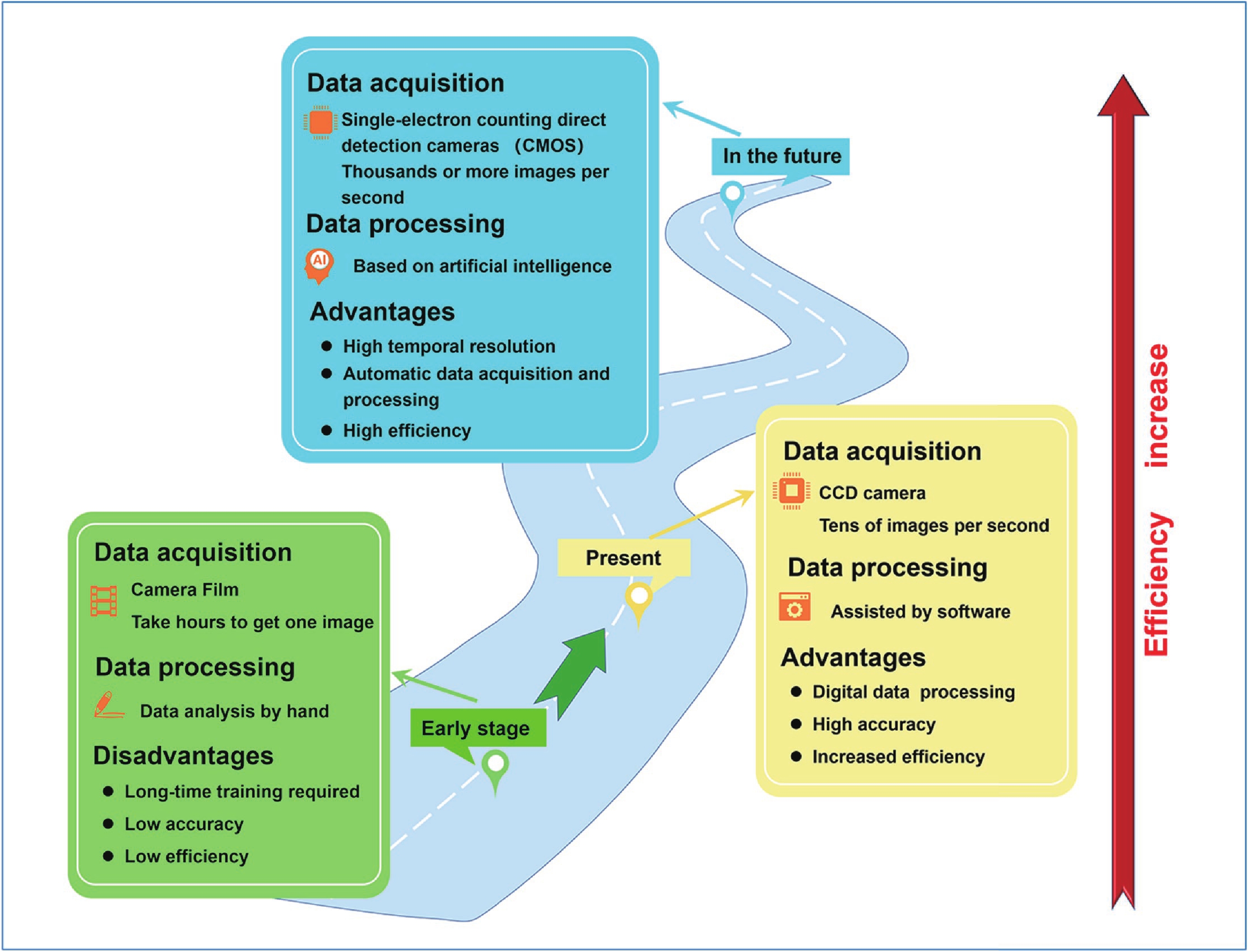
Fig. 1.  (Color online) The evolution of TEM data acquisition and processing.

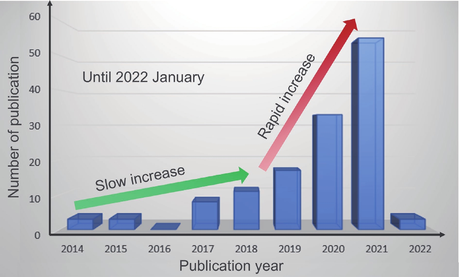
Fig. 2.  (Color online) Publications from the Web of Science with the keywords of TEM and machine learning.

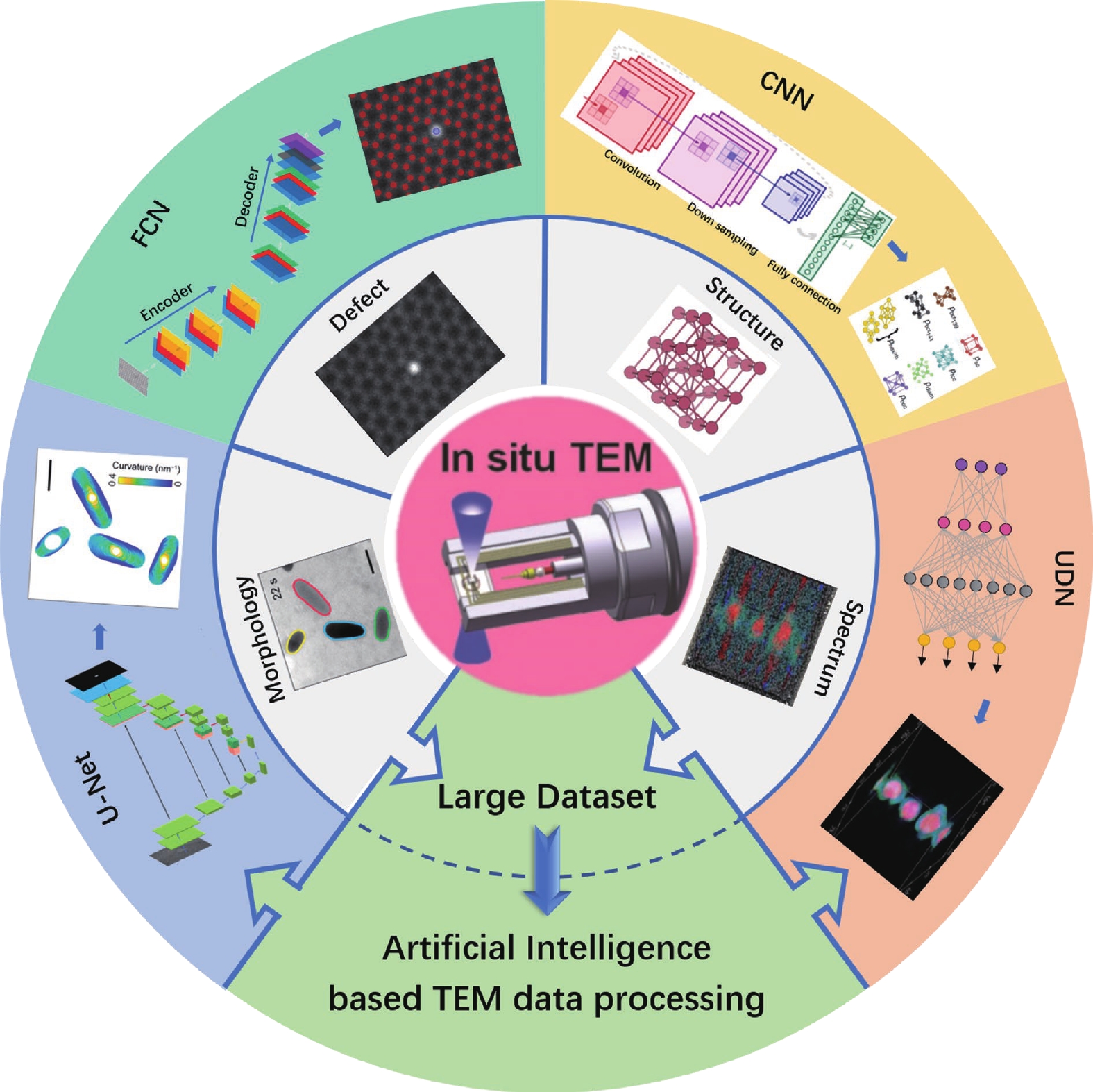
Fig. 3.  (Color online) Application of artificial intelligence for high-efficient processing of various TEM datasets. FCN, CNN, and UDN are short for fully convolution network, convolutional neural network, and unsupervised deep network, respectively.

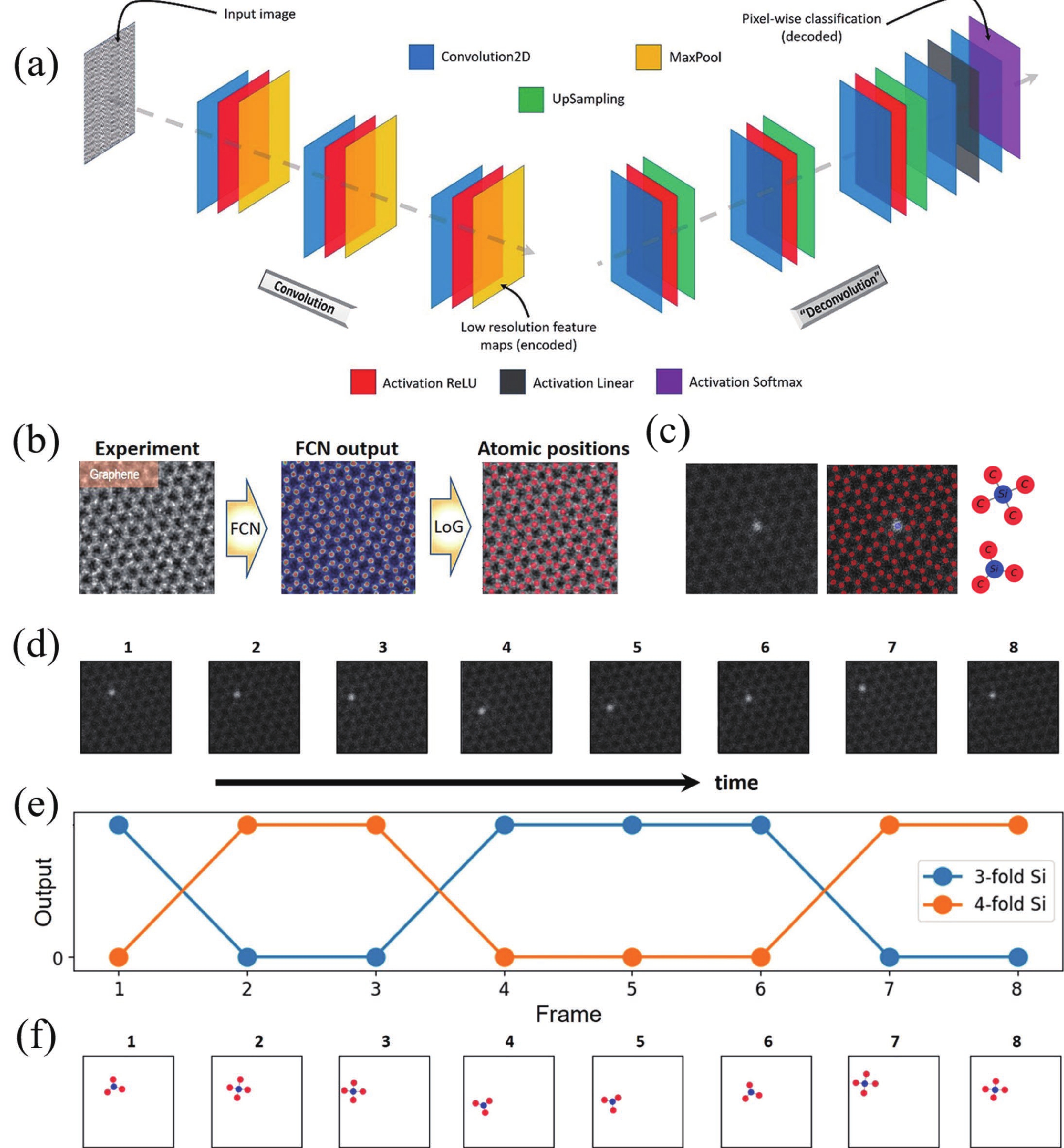
Fig. 4.  (Color online) The introduction of a neural network in the analysis of atomic defects[72]. (a) Schematic architecture of a CNN with an encoder-decoder structure. (b) Location of carbon atoms of graphene. (c) The extracted dopant Si atoms and, in this way, the classification between 3-fold and 4-fold Si defects is conducted. (d) The evolution of the same Si dopant on the time scale. (e) Classification of defect types. (f) Extraction of the defect from STEM images.

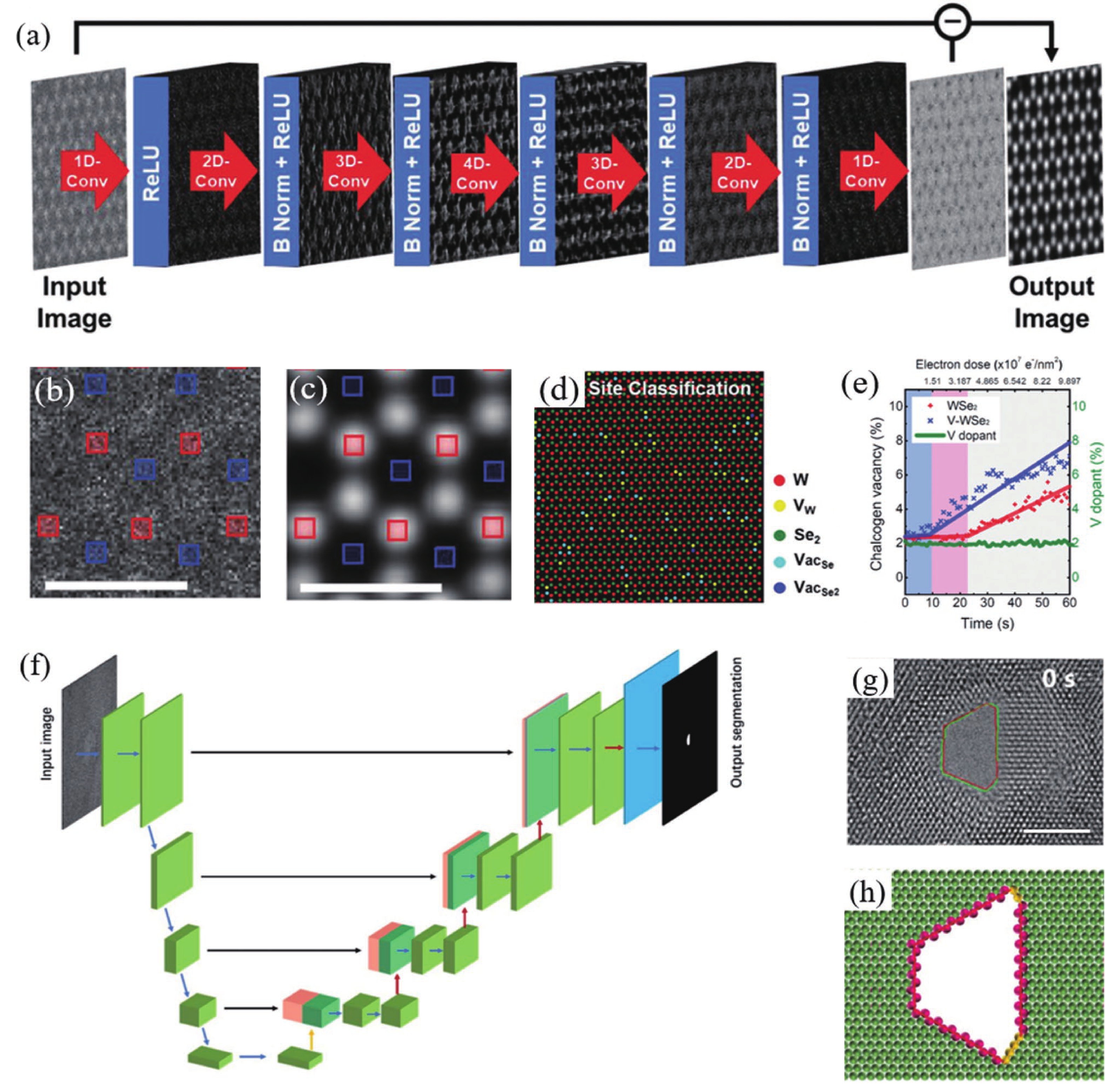
Fig. 5.  (Color online) Introduction of CNN-based algorithm for atomic-scale identification of point and line defects[61, 64]. (a) A CNN as a denoiser process. (b, c) Comparison of the signal-to-noise between the unprocessed and processed images. (d) Defect mapping of STEM image. (e) The statistics of Se vacancies and V dopants change according to the electron beam irradiation time. The scale bar is 5 nm. (f) The architecture of U-Net. (g, h) The border recognition of a nanopore.

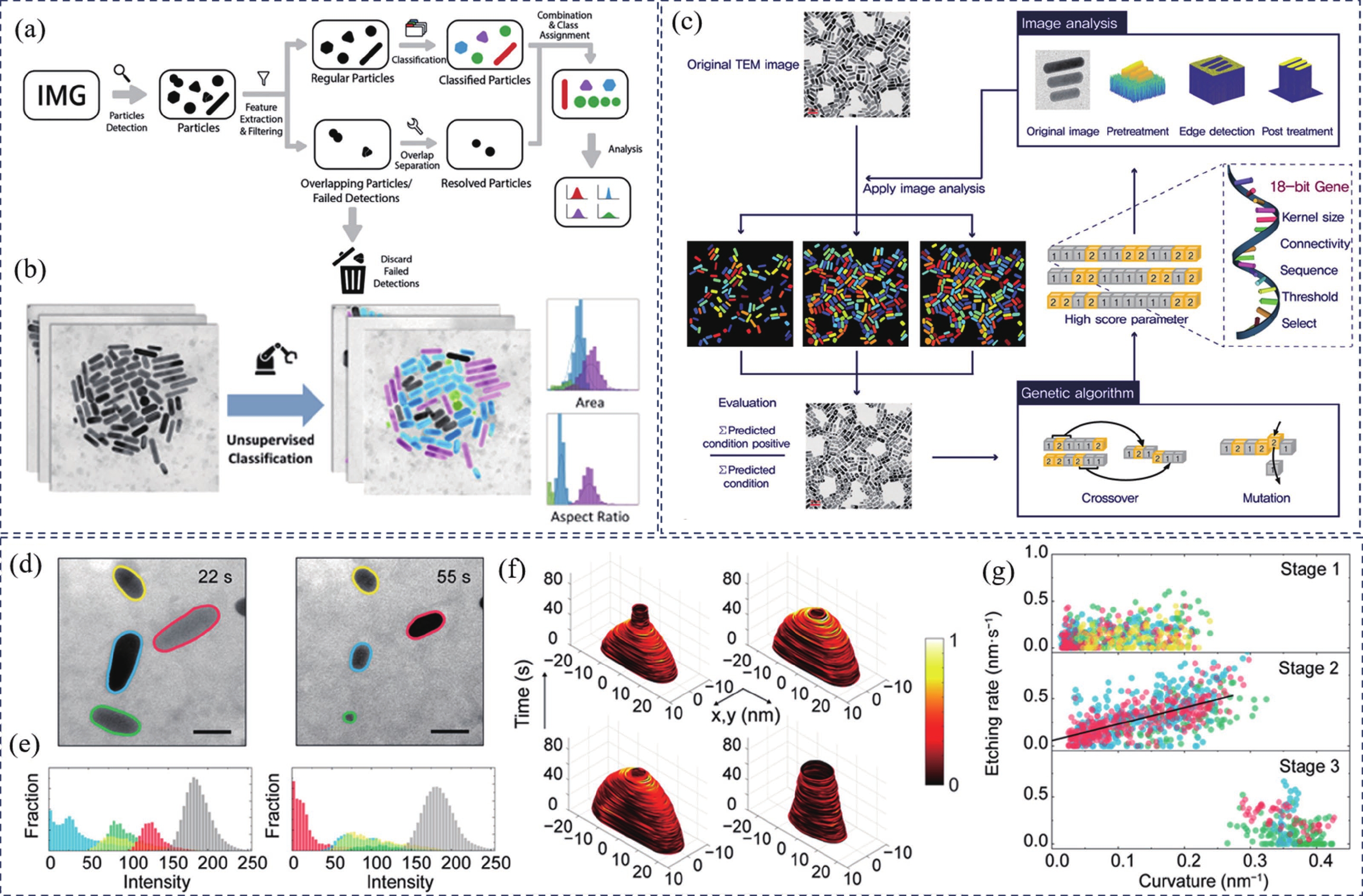
Fig. 6.  (Color online) Introduction of two machine learning based methods in morphology analysis of gold particles[63, 68, 70]. (a, b) A complete unsupervised clustering algorithm utilized in classification of gold nanorods. (c) A GA containing various image analysis methods as genes to explore the morphological characteristics of NPs. (d) NPs segmented by U-Net with boundaries. (e) The intensity of the four types of NPs and the background in the TEM images explored by U-Net. (f) Boundaries of NPs colored to their local etching rates and the etching time indicate the height. (g) The three etching stages defined by the relationships between the etching rate and curvature.

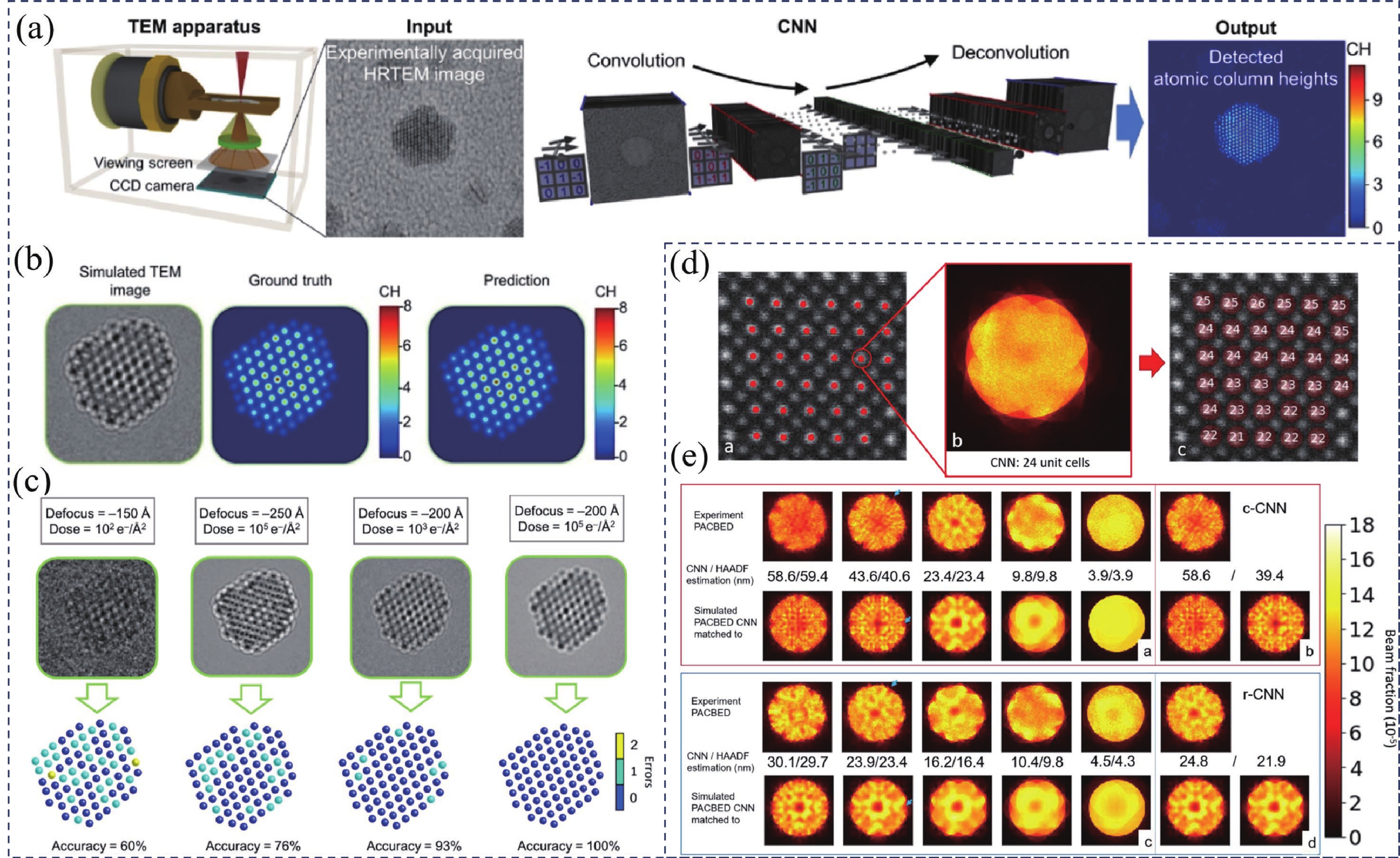
Fig. 7.  (Color online) Application of machine learning based methods in the analysis of atomic column heights. (a) A CNN illustration as an example of the supervised network utilized in the analysis. (b) Comparison between ground truth and prediction after regression and classification on STEM images. (c) Results of the network with various defocus values and electron dose. (d) The sub-unit cell calculated and mapped from a 4D-STEM dataset. (e) Comparison between c-CNN and r-CNN measurement and HAADF estimation.

Fig. 8.  (Color online) Application of CNN in structure analysis. (a) The workflow of deploying a neural network model to automatically classify structure. (b–d) Two-dimensional diffraction patterns of different crystal structures are divided into eight classes in SAED. (e) An illustration of a CNN(LeNet-5) with a computer-simulated training dataset. (f) Comparison between manual and automatic classification. (g) Correlation matrix of the results of the two methods.

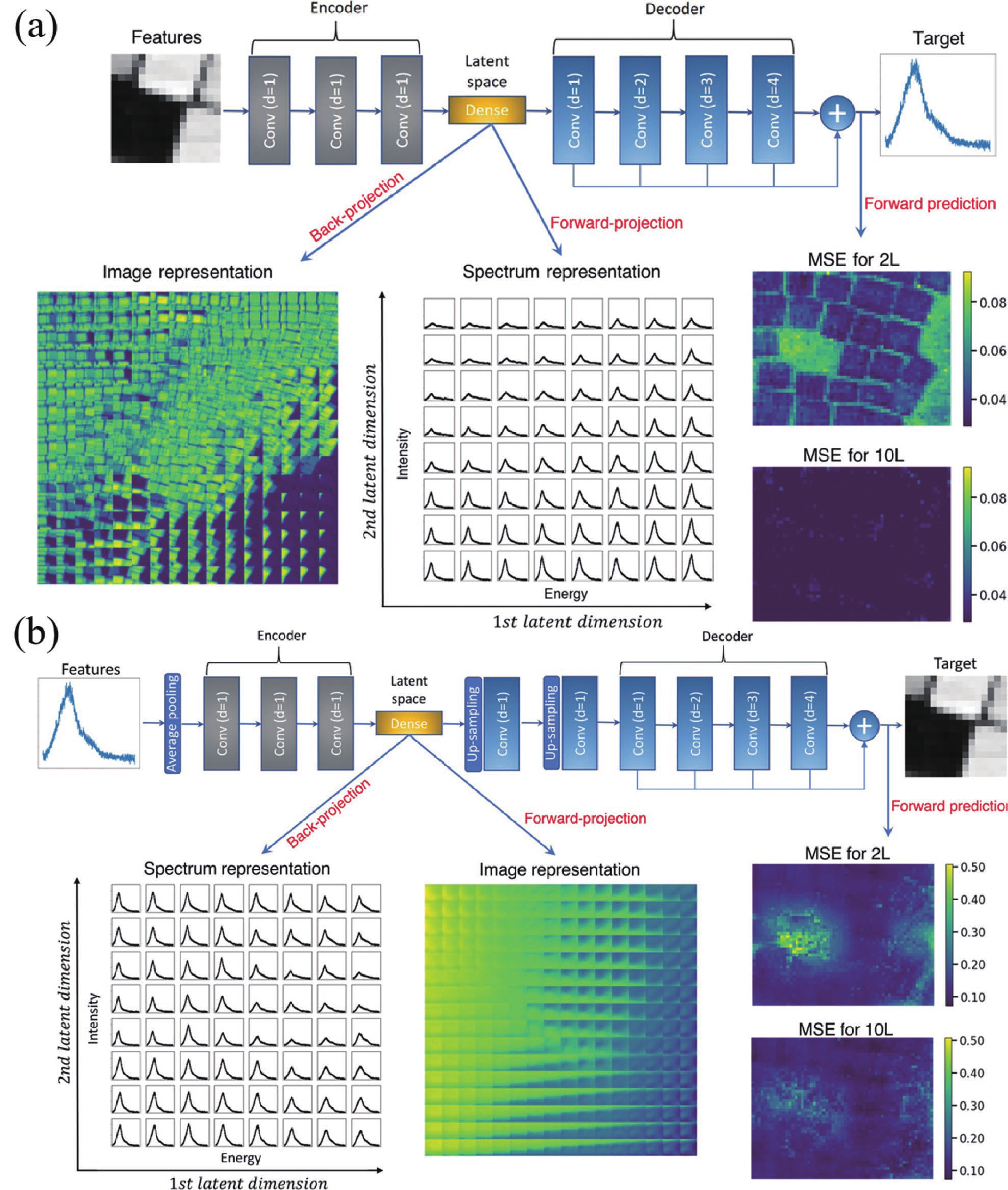
Fig. 9.  (Color online) Introduction of the use of a neural network to explore the correlative laws between local geometries and plasmon responses[65]. (a) The im2spec network, in which subimages are taken as features and spectra are taken as targets. (b) The spec2im network, which is trained with HAADF spatial descriptors and corresponding spectral descriptors, similar to the im2spec network. However, the spectra are used as features and subimages are used as targets.

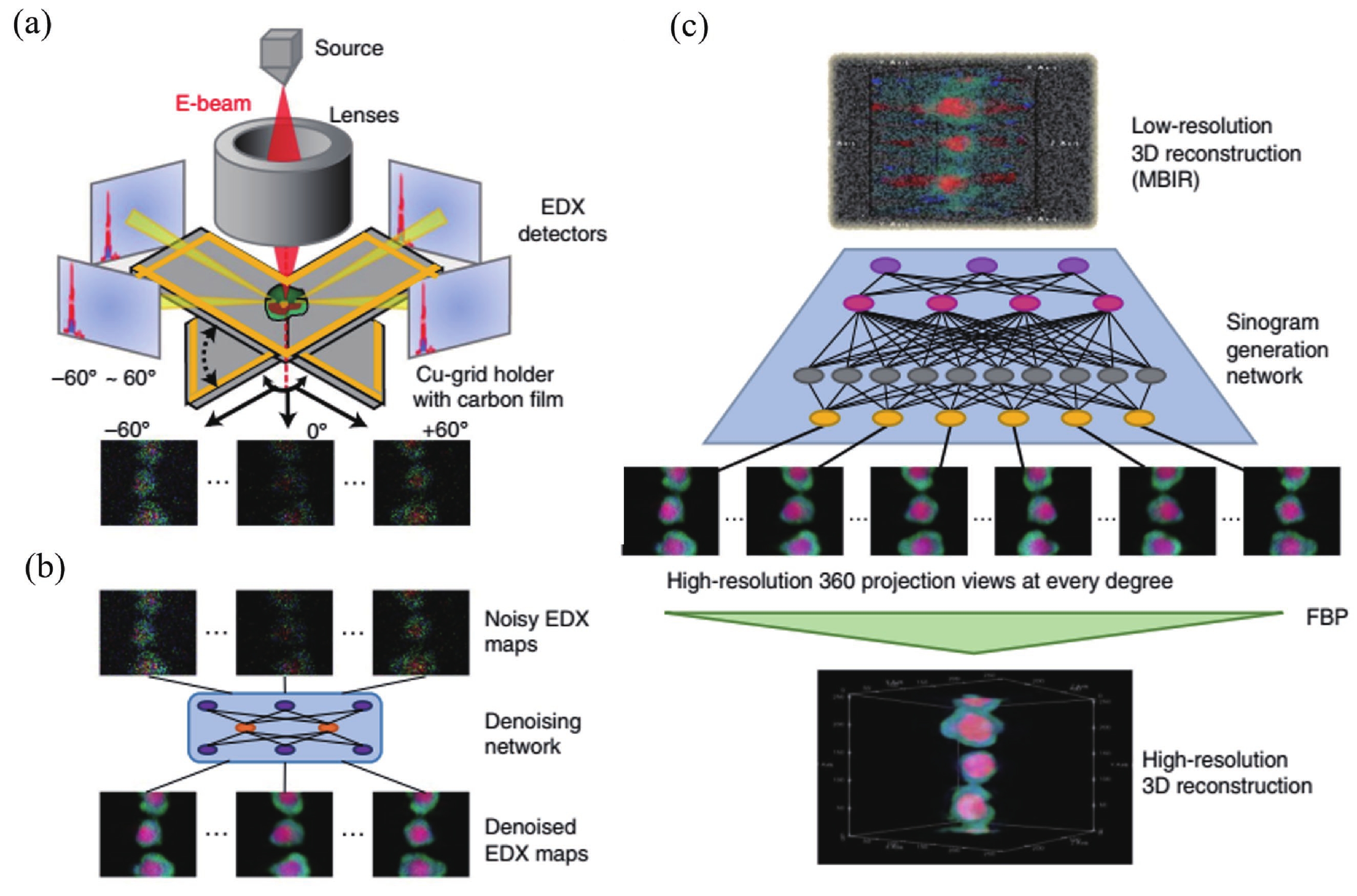
Fig. 10.  (Color online) The work flow of the 3D construction of STEM energy-dispersive X-ray spectroscopy (STEM-EDX) by deep learning[67]. (a) Collection of raw EDX experimental maps. (b) A denoising network to improve the noisy EDX maps. (c) Unsupervised deep network to generate high-quality 3D reconstruction.

Table 1.   The main parameters of TEM data analysis that is based on machine learning of different types of material properties.

ClassificationAlgorithmData typeTraining
Dataset
Testing
Dataset
AccuracyRef.
DefectFCN (weakly supervised)STEMSimulationExperiment~97%[64]
CNN and U-Net (supervised)STEMSimulationExperiment98%[64]
U-Net (supervised)STEMSimulationSimulation[66]
U-Net (supervised)HRTEMExperimentExperiment93.17%[61]
MorphologyAutoDetect-mNP (unsupervised)TEMExperimentExperiment85%–95%[68]
FCN (regression&classification)STEMSimulationSimulation85%–93%[69]
CNNSTEMSimulationSimulation95%[60]
U-NetTEMExperimentExperiment[63]
Genetic algorithmTEMExperimentExperiment99.75%[70]
StructureCNNFFTSimulationSimulation>97%[62]
CNNHRTEMSimulationSimulation90.5%[71]
SpectrumU-NetEELSExperimentExperiment>90%[65]
Neural network (unsupervised)EDXExperimentExperiment[67]
DownLoad: CSV
[1]
Avsar A, Ciarrocchi A, Pizzochero M, et al. Defect induced, layer-modulated magnetism in ultrathin metallic PtSe2. Nat Nanotechnol, 2019, 14, 674 doi: 10.1038/s41565-019-0467-1
[2]
Zhou M, Wang W, Lu J, et al. How defects influence the photoluminescence of TMDCs. Nano Res, 2021, 14, 29 doi: 10.1007/s12274-020-3037-9
[3]
Jiang J, Ni Z. Defect engineering in two-dimensional materials. J Semicond, 2019, 40, 070403 doi: 10.1088/1674-4926/40/7/070403
[4]
Chen X, Du F, Wang C, et al. Direct visualization of breakdown-induced metal migration in enhanced modified lateral silicon-controlled rectifiers. IEEE Trans Electron Devices, 2021, 68, 1378 doi: 10.1109/TED.2021.3053501
[5]
Wu X, Luo C, Hao P, et al. Probing and manipulating the interfacial defects of InGaAs dual-layer metal oxides at the atomic scale. Adv Mater, 2018, 30, 1703025 doi: 10.1002/adma.201703025
[6]
Luo C, Wang C, Wu X, et al. In situ transmission electron microscopy characterization and manipulation of two-dimensional layered materials beyond graphene. Small, 2017, 13, 1604259 doi: 10.1002/smll.201604259
[7]
Mendes R G, Pang J, Bachmatiuk A, et al. Electron-driven in situ transmission electron microscopy of 2D transition metal dichalcogenides and their 2D heterostructures. ACS Nano, 2019, 13, 978 doi: 10.1021/acsnano.8b08079
[8]
Dong Z, Ma Y. Atomic-level handedness determination of chiral crystals using aberration-corrected scanning transmission electron microscopy. Nat Commun, 2020, 11, 1588 doi: 10.1038/s41467-020-15388-5
[9]
Zaluzec N J. The influence of Cs/Cc correction in analytical imaging and spectroscopy in scanning and transmission electron microscopy. Ultramicroscopy, 2015, 151, 240 doi: 10.1016/j.ultramic.2014.09.012
[10]
Lin Y, Zhou M, Tai X, et al. Analytical transmission electron microscopy for emerging advanced materials. Matter, 2021, 4, 2309 doi: 10.1016/j.matt.2021.05.005
[11]
Zhang J, Yu Y, Wang P, et al. Characterization of atomic defects on the photoluminescence in two-dimensional materials using transmission electron microscope. InfoMat, 2019, 1, 85 doi: 10.1002/inf2.12002
[12]
Kim B H, Yang J, Lee D, et al. Liquid-phase transmission electron microscopy for studying colloidal inorganic nanoparticles. Adv Mater, 2018, 30, 1703316 doi: 10.1002/adma.201703316
[13]
Fan Z, Zhang L, Baumann D, et al. In situ transmission electron microscopy for energy materials and devices. Adv Mater, 2019, 31, 1900608 doi: 10.1002/adma.201900608
[14]
Yang X, Luo C, Tian X Y, et al. A review of in situ transmission electron microscopy study on the switching mechanism and packaging reliability in non-volatile memory. J Semicond, 2021, 42, 013102 doi: 10.1088/1674-4926/42/1/013102
[15]
Zhang C, Larionov K V, Firestein K L, et al. Optomechanical properties of MoSe2 nanosheets as revealed by in situ transmission electron microscopy. Nano Lett, 2022, 22, 673 doi: 10.1021/acs.nanolett.1c03796
[16]
de Jonge N, Houben L, Dunin-Borkowski R E, et al. Resolution and aberration correction in liquid cell transmission electron microscopy. Nat Rev Mater, 2019, 4, 61 doi: 10.1038/s41578-018-0071-2
[17]
Xu H, Wu X, Tian X, et al. Dynamic structure-properties characterization and manipulation in advanced nanodevices. Mater Today Nano, 2019, 7, 100042 doi: 10.1016/j.mtnano.2019.100042
[18]
Cai J S, Cai R, Sun Z T, et al. Confining TiO2 nanotubes in PECVD-enabled graphene capsules toward ultrafast K-ion storage: in situ TEM/XRD study and DFT analysis. Nano-Micro Lett, 2020, 12, 123 doi: 10.1007/s40820-020-00460-y
[19]
Wang R B, Song Z T, Song W X, et al. Phase-change memory based on matched Ge-Te, Sb-Te, and In-Te octahedrons: Improved electrical performances and robust thermal stability. Infomat, 2021, 3, 1008 doi: 10.1002/inf2.12233
[20]
Wang Y H, Pang J B, Cheng Q L, et al. Applications of 2D-layered palladium diselenide and its van der Waals heterostructures in electronics and optoelectronics. Nano-Micro Lett, 2021, 13, 143 doi: 10.1007/s40820-021-00660-0
[21]
Wu Y L, Gaddam R R, Zhang C, et al. Stabilising cobalt sulphide nanocapsules with nitrogen-doped carbon for high-performance sodium-ion storage. Nano-Micro Lett, 2020, 12, 48 doi: 10.1007/s40820-020-0391-9
[22]
Zhang H, Yang Y, Xu H, et al. Li4Ti5O12 spinel anode: Fundamentals and advances in rechargeable batteries. Infomat, 2021, 4, e12228 doi: 10.1002/inf2.12228
[23]
Ibrahim I, Kalbacova J, Engemaier V, et al. Confirming the dual role of etchants during the enrichment of semiconducting single wall carbon nanotubes by chemical vapor deposition. Chem Mater, 2015, 27, 5964 doi: 10.1021/acs.chemmater.5b02037
[24]
Pang J, Wang Y, Yang X, et al. A wafer-scale two-dimensional platinum monosulfide ultrathin film via metal sulfurization for high performance photoelectronics. Mater Adv, 2022, 3, 1497 doi: 10.1039/D1MA00757B
[25]
Sun Y, Sun B, He J B, et al. Compositional and structural engineering of inorganic nanowires toward advanced properties and applications. Infomat, 2019, 1, 496 doi: 10.1002/inf2.12049
[26]
Wang J W, Jia Z R, Liu X H, et al. Construction of 1D heterostructure NiCo@C/ZnO nanorod with enhanced microwave absorption. Nano-Micro Lett, 2021, 13, 175 doi: 10.1007/s40820-021-00704-5
[27]
Yu B J, Liu S D, Xie W H, et al. Versatile core-shell magnetic fluorescent mesoporous microspheres for multilevel latent fingerprints magneto-optic information recognition. Infomat, 2022, 4, e12289 doi: 10.1002/inf2.12289
[28]
Schorb M, Haberbosch I, Hagen W J H, et al. Software tools for automated transmission electron microscopy. Nat Methods, 2019, 16, 471 doi: 10.1038/s41592-019-0396-9
[29]
Plotkin-Swing B, Corbin G J, De Carlo S, et al. Hybrid pixel direct detector for electron energy loss spectroscopy. Ultramicroscopy, 2020, 217, 113067 doi: 10.1016/j.ultramic.2020.113067
[30]
Maigné A, Wolf M. Low-dose electron energy-loss spectroscopy using electron counting direct detectors. Microscopy, 2018, 67, i86 doi: 10.1093/jmicro/dfx088
[31]
Chen X, Zhou L H, Wang P, et al. Effects associated with nanostructure fabrication using in situ liquid cell TEM technology. Nano-Micro Lett, 2015, 7, 385 doi: 10.1007/s40820-015-0054-4
[32]
Zhang S, Pang J B, Cheng Q L, et al. High-performance electronics and optoelectronics of monolayer tungsten diselenide full film from pre-seeding strategy. Infomat, 2021, 3, 1455 doi: 10.1002/inf2.12259
[33]
Ishida T, Shinozaki A, Kuwahara M, et al. Performance of a silicon-on-insulator direct electron detector in a low-voltage transmission electron microscope. Microscopy, 2021, 70, 321 doi: 10.1093/jmicro/dfaa072
[34]
Ophus C, Ciston J, Pierce J, et al. Efficient linear phase contrast in scanning transmission electron microscopy with matched illumination and detector interferometry. Nat Commun, 2016, 7, 10719 doi: 10.1038/ncomms10719
[35]
Hui F, Li C, Chen Y H, et al. Understanding the structural evolution of Au/WO2.7 compounds in hydrogen atmosphere by atomic scale in situ environmental TEM. Nano Res, 2020, 13, 3019 doi: 10.1007/s12274-020-2966-7
[36]
Jiang Y, Zhang Z F, Yuan W T, et al. Recent advances in gas-involved in situ studies via transmission electron microscopy. Nano Res, 2018, 11, 42 doi: 10.1007/s12274-017-1645-9
[37]
Wang Y, Peng X X, Abelson A, et al. In situ TEM observation of neck formation during oriented attachment of PbSe nanocrystals. Nano Res, 2019, 12, 2549 doi: 10.1007/s12274-019-2483-8
[38]
Weng B, Jiang Y H, Liao H G, et al. Visualizing light-induced dynamic structural transformations of Au clusters-based photocatalyst via in situ TEM. Nano Res, 2021, 14, 2805 doi: 10.1007/s12274-021-3289-z
[39]
Zhu Y T, Yuan D D, Zhang H, et al. Atomic-scale insights into the formation of 2D crystals from in situ transmission electron microscopy. Nano Res, 2021, 14, 1650 doi: 10.1007/s12274-020-3034-z
[40]
Alberti A, Bongiorno C, Smecca E, et al. Pb clustering and PbI2 nanofragmentation during methylammonium lead iodide perovskite degradation. Nat Commun, 2019, 10, 2196 doi: 10.1038/s41467-019-09909-0
[41]
Spurgeon S R, Ophus C, Jones L, et al. Towards data-driven next-generation transmission electron microscopy. Nat Mater, 2020, 20, 274 doi: 10.1038/s41563-020-00833-z
[42]
Kalinin S V, Lupini A R, Dyck O, et al. Lab on a beam—Big data and artificial intelligence in scanning transmission electron microscopy. MRS Bull, 2019, 44, 565 doi: 10.1557/mrs.2019.159
[43]
Uesugi F, Koshiya S, Kikkawa J, et al. Non-negative matrix factorization for mining big data obtained using four-dimensional scanning transmission electron microscopy. Ultramicroscopy, 2021, 221, 113168 doi: 10.1016/j.ultramic.2020.113168
[44]
Dyck O, Ziatdinov M, Lingerfelt D B, et al. Atom-by-atom fabrication with electron beams. Nat Rev Mater, 2019, 4, 497 doi: 10.1038/s41578-019-0118-z
[45]
Chen M, Dai W, Sun S Y, et al. Convolutional neural networks for automated annotation of cellular cryo-electron tomograms. Nat Methods, 2017, 14, 983 doi: 10.1038/nmeth.4405
[46]
Lee C H, Khan A, Luo D, et al. Deep learning enabled strain mapping of single-atom defects in two-dimensional transition metal dichalcogenides with sub-picometer precision. Nano Lett, 2020, 20, 3369 doi: 10.1021/acs.nanolett.0c00269
[47]
Vasudevan R K, Ziatdinov M, Jesse S, et al. Phases and interfaces from real space atomically resolved data: physics-based deep data image analysis. Nano Lett, 2016, 16, 5574 doi: 10.1021/acs.nanolett.6b02130
[48]
Belianinov A, He Q, Kravchenko M, et al. Identification of phases, symmetries and defects through local crystallography. Nat Commun, 2015, 6, 7801 doi: 10.1038/ncomms8801
[49]
Nelson C T, Vasudevan R K, Zhang X, et al. Exploring physics of ferroelectric domain walls via Bayesian analysis of atomically resolved STEM data. Nat Commun, 2020, 11, 6361 doi: 10.1038/s41467-020-19907-2
[50]
LeCun Y, Boser B, Denker J S, et al. Backpropagation applied to handwritten zip code recognition. Neural Comput, 1989, 1, 541 doi: 10.1162/neco.1989.1.4.541
[51]
Krizhevsky A, Sutskever I, Hinton G E. ImageNet classification with deep convolutional neural networks. Proceedings of the 25th International Conference on Neural Information Processing Systems - Volume 1, 2012, 1097
[52]
Ronneberger O, Fischer P, Brox T. U-Net: convolutional networks for biomedical image segmentation. Medical Image Computng and Computer-Assisted Intervention – MICCAI 2015, Springer International Publishing, 2015, 234
[53]
LeCun Y, Bengio Y, Hinton G. Deep learning. Nature, 2015, 521, 436 doi: 10.1038/nature14539
[54]
Chen L C, Zhu Y, Papandreou G, et al. Encoder-decoder with atrous separable convolution for semantic image segmentation. Proceedings of the 15th European Conference on Computer Vision (ECCV), 2018
[55]
Ge M, Su F, Zhao Z, et al. Deep learning analysis on microscopic imaging in materials science. Mater Today Nano, 2020, 11, 100087 doi: 10.1016/j.mtnano.2020.100087
[56]
Dan J, Zhao X, Pennycook S J. A machine perspective of atomic defects in scanning transmission electron microscopy. InfoMat, 2019, 1, 359 doi: 10.1002/inf2.12026
[57]
Li W, Field K G, Morgan D. Automated defect analysis in electron microscopic images. npj Comput Mater, 2018, 4, 36 doi: 10.1038/s41524-018-0093-8
[58]
Maksov A, Dyck O, Wang K, et al. Deep learning analysis of defect and phase evolution during electron beam-induced transformations in WS2. npj Comput Mater, 2019, 5, 12 doi: 10.1038/s41524-019-0152-9
[59]
Ede J M, Beanland R. Partial scanning transmission electron microscopy with deep learning. Sci Rep, 2020, 10, 8332 doi: 10.1038/s41598-020-65261-0
[60]
Zhang C, Feng J, DaCosta L R, et al. Atomic resolution convergent beam electron diffraction analysis using convolutional neural networks. Ultramicroscopy, 2019, 210, 112921 doi: 10.1017/S1431927619001375
[61]
Wang C, Zou Q, Cheng Z, et al. Tailoring atomic 1T phase CrTe2 for in situ fabrication. Nanotechnology, 2021, 33, 085302 doi: 10.1088/1361-6528/ac3a3a
[62]
Ziletti A, Kumar D, Scheffler M, et al. Insightful classification of crystal structures using deep learning. Nat Commun, 2018, 9, 2775 doi: 10.1038/s41467-018-05169-6
[63]
Yao L, Ou Z, Luo B, et al. Machine learning to reveal nanoparticle dynamics from liquid-phase TEM videos. ACS Cent Sci, 2020, 6, 1421 doi: 10.1021/acscentsci.0c00430
[64]
Yang S H, Choi W, Cho B W, et al. Deep learning-assisted quantification of atomic dopants and defects in 2D materials. Adv Sci, 2021, 8, 2101099 doi: 10.1002/advs.202101099
[65]
Roccapriore K M, Ziatdinov M, Cho S H, et al. Predictability of localized plasmonic responses in nanoparticle assemblies. Small, 2021, 17, 2100181 doi: 10.1002/smll.202100181
[66]
Kalinin S V, Dyck O, Jesse S, et al. Exploring order parameters and dynamic processes in disordered systems via variational autoencoders. Sci Adv, 2021, 7, eabd5084 doi: 10.1126/sciadv.abd5084
[67]
Han Y, Jang J, Cha E, et al. Deep learning STEM-EDX tomography of nanocrystals. Nat Mach Intell, 2021, 3, 267 doi: 10.1038/s42256-020-00289-5
[68]
Wang X, Li J, Ha H D, et al. Autodetect-mNP: an unsupervised machine learning algorithm for automated analysis of transmission electron microscope images of metal nanoparticles. J Am Chem Soc, 2021, 1, 316 doi: 10.1021/jacsau.0c00030
[69]
Ragone M, Yurkiv V, Song B, et al. Atomic column heights detection in metallic nanoparticles using deep convolutional learning. Comput Mater Sci, 2020, 180, 109722 doi: 10.1016/j.commatsci.2020.109722
[70]
Lee B, Yoon S, Lee J W, et al. Statistical characterization of the morphologies of nanoparticles through machine learning based electron microscopy image analysis. ACS Nano, 2020, 14, 17125 doi: 10.1021/acsnano.0c06809
[71]
Förster G D, Castan A, Loiseau A, et al. A deep learning approach for determining the chiral indices of carbon nanotubes from high-resolution transmission electron microscopy images. Carbon, 2020, 169, 465 doi: 10.1016/j.carbon.2020.06.086
[72]
Ziatdinov M, Dyck O, Maksov A, et al. Deep learning of atomically resolved scanning transmission electron microscopy images: Chemical identification and tracking local transformations. ACS Nano, 2017, 11, 12742 doi: 10.1021/acsnano.7b07504
[73]
Li W S, Ning H K, Yu Z H, et al. Reducing the power consumption of two-dimensional logic transistors. J Semicond, 2019, 40, 091002 doi: 10.1088/1674-4926/40/9/091002
[74]
Wang J L. A novel spin-FET based on 2D antiferromagnet. J Semicond, 2019, 40, 020401 doi: 10.1088/1674-4926/40/2/020401
[75]
Liang F, Wang C, Luo C, et al. Ferromagnetic CoSe broadband photodetector at room temperature. Nanotechnology, 2020, 31, 374002 doi: 10.1088/1361-6528/ab9867
[76]
Zhang H, Jiang X T, Wang Y L, et al. Preface to the special issue on monoelemental 2D semiconducting materials and their applications. J Semicond, 2020, 41, 080101 doi: 10.1088/1674-4926/41/8/080101
[77]
Zhou J S, Yang J H, Wei Z M. Photodetectors based on 2D material/Si heterostructure. J Semicond, 2020, 41, 080401 doi: 10.1088/1674-4926/41/8/080401
[78]
Deng N Q, Tian H, Zhang J, et al. Black phosphorus junctions and their electrical and optoelectronic applications. J Semicond, 2021, 42, 081001 doi: 10.1088/1674-4926/42/8/081001
[79]
Wang C L, Wu X, Ma Y H, et al. Metallic few-layered VSe2 nanosheets: high two-dimensional conductivity for flexible in-plane solid-state supercapacitors. J Mater Chem A, 2018, 6, 8299 doi: 10.1039/C8TA00089A
[80]
Wang C, Wu X, Zhang X, et al. Iron-doped VSe2 nanosheets for enhanced hydrogen evolution reaction. Appl Phys Lett, 2020, 116, 223901 doi: 10.1063/5.0008092
[81]
Qiu H, Xu T, Wang Z, et al. Hopping transport through defect-induced localized states in molybdenum disulphide. Nat Commun, 2013, 4, 2642 doi: 10.1038/ncomms3642
[82]
Wang C, Jin M, Liu D, et al. VSe2 quantum dots with high-density active edges for flexible efficient hydrogen evolution reaction. J Phys D, 2021, 54, 214006 doi: 10.1088/1361-6463/abe78d
[83]
Zhang S, Wang C G, Li M Y, et al. Defect structure of localized excitons in a WSe2 monolayer. Phys Rev Lett, 2017, 119, 046101 doi: 10.1103/PhysRevLett.119.046101
[84]
Wang X, Zhang Y, Si H, et al. Single-atom vacancy defect to trigger high-efficiency hydrogen evolution of MoS2. J Am Chem Soc, 2020, 142, 4298 doi: 10.1021/jacs.9b12113
[85]
Barthelmi K, Klein J, Hötger A, et al. Atomistic defects as single-photon emitters in atomically thin MoS2. Appl Phys Lett, 2020, 117, 070501 doi: 10.1063/5.0018557
[86]
Susi T, Meyer J C, Kotakoski J. Manipulating low-dimensional materials down to the level of single atoms with electron irradiation. Ultramicroscopy, 2017, 180, 163 doi: 10.1016/j.ultramic.2017.03.005
[87]
Pennycook S J, Jesson D E. High-resolution Z-contrast imaging of crystals. Ultramicroscopy, 1991, 37, 14 doi: 10.1016/0304-3991(91)90004-P
[88]
Boyes E D, LaGrow A P, Ward M R, et al. Single atom dynamics in chemical reactions. Acc Chem Res, 2020, 53, 390 doi: 10.1021/acs.accounts.9b00500
[89]
Mi R, Li D, Hu Z, et al. Morphology effects of CeO2 nanomaterials on the catalytic combustion of toluene: a combined kinetics and diffuse reflectance infrared fourier transform spectroscopy study. ACS Catal, 2021, 11, 7876 doi: 10.1021/acscatal.1c01981
[90]
Ni B, Wang X. Face the edges: catalytic active sites of nanomaterials. Adv Sci, 2015, 2, 1500085 doi: 10.1002/advs.201500085
[91]
Zheng H M. Imaging, understanding, and control of nanoscale materials transformations. MRS Bull, 2021, 46, 443 doi: 10.1557/s43577-021-00113-4
[92]
Wang W H, Chee S W, Yan H W, et al. Growth dynamics of vertical and lateral layered double hydroxide nanosheets during electrodeposition. Nano Lett, 2021, 21, 5977 doi: 10.1021/acs.nanolett.1c00898
[93]
Shi F, Peng J, Li F, et al. Design of highly durable core−shell catalysts by controlling shell distribution guided by in situ corrosion study. Adv Mater, 2021, 33, 2101511 doi: 10.1002/adma.202101511
[94]
Ou Z, Wang Z, Luo B, et al. Kinetic pathways of crystallization at the nanoscale. Nat Mater, 2020, 19, 450 doi: 10.1038/s41563-019-0514-1
[95]
Hauwiller M R, Ye X, Jones M R, et al. Tracking the effects of ligands on oxidative etching of gold nanorods in graphene liquid cell electron microscopy. ACS Nano, 2020, 14, 10239 doi: 10.1021/acsnano.0c03601
[96]
Shan H, Gao W, Xiong Y, et al. Nanoscale kinetics of asymmetrical corrosion in core-shell nanoparticles. Nat Commun, 2018, 9, 1011 doi: 10.1038/s41467-018-03372-z
[97]
Liao H G, Zherebetskyy D, Xin H, et al. Facet development during platinum nanocube growth. Science, 2014, 345, 916 doi: 10.1126/science.1253149
[98]
Wang F K, Yang S J, Zhai T Y. 2D Bi2Se3 materials for optoelectronics. iScience, 2021, 24, 103291 doi: 10.1016/j.isci.2021.103291
[99]
Li Q, Lu J, Gupta P, et al. Engineering optical absorption in graphene and other 2D materials: Advances and applications. Adv Opt Mater, 2019, 7, 1900595 doi: 10.1002/adom.201900595
[100]
Qiao J, Kong X, Hu Z X, et al. High-mobility transport anisotropy and linear dichroism in few-layer black phosphorus. Nat Commun, 2014, 5, 4475 doi: 10.1038/ncomms5475
[101]
O'Leary C M, Allen C S, Huang C, et al. Phase reconstruction using fast binary 4D STEM data. Appl Phys Lett, 2020, 116, 124101 doi: 10.1063/1.5143213
[102]
Flannigan D J, Zewail A H. 4D electron microscopy: principles and applications. Acc Chem Res, 2012, 45, 1828 doi: 10.1021/ar3001684
[103]
Zeltmann S E, Muller A, Bustillo K C, et al. Patterned probes for high precision 4D-STEM bragg measurements. Ultramicroscopy, 2020, 209, 112890 doi: 10.1016/j.ultramic.2019.112890
[104]
Koch C. Determination of core structure periodicity and point defect density along dislocations. PhD Thesis, Arizona State University, 2002
[105]
Su J, Wang M, Li Y, et al. Sub-millimeter-scale monolayer p-type H-phase VS2. Adv Funct Mater, 2020, 16, 2000240 doi: 10.1002/adfm.202000240
[106]
Ji Q, Li C, Wang J, et al. Metallic vanadium disulfide nanosheets as a platform material for multifunctional electrode applications. Nano Lett, 2017, 17, 4908 doi: 10.1021/acs.nanolett.7b01914
[107]
Tao L, Chen K, Chen Z, et al. Centimeter-scale CVD growth of highly crystalline single-layer MoS2 film with spatial homogeneity and the visualization of grain boundaries. ACS Appl Mater Interfaces, 2017, 9, 12073 doi: 10.1021/acsami.7b00420
[108]
Acerce M, Voiry D, Chhowalla M. Metallic 1T phase MoS2 nanosheets as supercapacitor electrode materials. Nat Nanotechnol, 2015, 10, 313 doi: 10.1038/nnano.2015.40
[109]
Teich D, Seifert G, Iijima S, et al. Helicity in ropes of chiral nanotubes: calculations and observation. Phys Rev Lett, 2012, 108, 235501 doi: 10.1103/PhysRevLett.108.235501
[110]
Tang M S Y, Ng E P, Juan J C, et al. Metallic and semiconducting carbon nanotubes separation using an aqueous two-phase separation technique: a review. Nanotechnology, 2016, 27, 332002 doi: 10.1088/0957-4484/27/33/332002
[111]
Warner J H, Lin Y C, He K, et al. Atomic level spatial variations of energy states along graphene edges. Nano Lett, 2014, 14, 6155 doi: 10.1021/nl5023095
[112]
Yin Z W, Zhao W, Li J, et al. Advanced electron energy loss spectroscopy for battery studies. Adv Funct Mater, 2022, 32, 2107190 doi: 10.1002/adfm.202107190
[113]
Pokle A, Coelho J, Macguire E, et al. EELS probing of lithium based 2D battery compounds processed by liquid phase exfoliation. Nano Energy, 2016, 30, 18 doi: 10.1016/j.nanoen.2016.09.021
[114]
Ali H, Maynau C, Lajaunie L, et al. Transmission electron microscopy and electron energy-loss spectroscopy studies of hole-selective molybdenum oxide contacts in silicon solar cells. ACS Appl Mater Interfaces, 2019, 11, 43075 doi: 10.1021/acsami.9b12703
[115]
Robertson A W, Lin Y C, Wang S, et al. Atomic structure and spectroscopy of single metal (Cr, V) substitutional dopants in monolayer MoS2. ACS Nano, 2016, 10, 10227 doi: 10.1021/acsnano.6b05674
[116]
Ramasse Q M, Seabourne C R, Kepaptsoglou D M, et al. Probing the bonding and electronic structure of single atom dopants in graphene with electron energy loss spectroscopy. Nano Lett, 2013, 13, 4989 doi: 10.1021/nl304187e
[117]
Zhang W, Seo D H, Chen T, et al. Kinetic pathways of ionic transport in fast-charging lithium titanate. Science, 2020, 367, 1030 doi: 10.1126/science.aax3520
[118]
Hage F S, Radtke G, Kepaptsoglou D M, et al. Single-atom vibrational spectroscopy in the scanning transmission electron microscope. Science, 2020, 367, 1124 doi: 10.1126/science.aba1136
[119]
Rehman Y A U, Po L M, Liu M. LiveNet: Improving features generalization for face liveness detection using convolution neural networks. Expert Syst Appl, 2018, 108, 159 doi: 10.1016/j.eswa.2018.05.004
[120]
Tong Z, Tanaka G. Hybrid pooling for enhancement of generalization ability in deep convolutional neural networks. Neurocomputing, 2019, 333, 76 doi: 10.1016/j.neucom.2018.12.036
[121]
Zheng S, Wang C, Yuan X, et al. Super-compression of large electron microscopy time series by deep compressive sensing learning. Patterns, 2021, 2, 100292 doi: 10.1016/j.patter.2021.100292
  • Search

    Advanced Search >>

    GET CITATION

    shu

    Export: BibTex EndNote

    Article Metrics

    Article views: 2447 Times PDF downloads: 278 Times Cited by: 0 Times

    History

    Received: 12 February 2022 Revised: 15 March 2022 Online: Accepted Manuscript: 20 May 2022Uncorrected proof: 25 May 2022Published: 01 August 2022

    Catalog

      Email This Article

      User name:
      Email:*请输入正确邮箱
      Code:*验证码错误
      Zhiheng Cheng, Chaolun Wang, Xing Wu, Junhao Chu. Review in situ transmission electron microscope with machine learning[J]. Journal of Semiconductors, 2022, 43(8): 081001. doi: 10.1088/1674-4926/43/8/081001 ****Zhiheng Cheng, Chaolun Wang, Xing Wu, Junhao Chu. 2022: Review in situ transmission electron microscope with machine learning. Journal of Semiconductors, 43(8): 081001. doi: 10.1088/1674-4926/43/8/081001
      Citation:
      Zhiheng Cheng, Chaolun Wang, Xing Wu, Junhao Chu. Review in situ transmission electron microscope with machine learning[J]. Journal of Semiconductors, 2022, 43(8): 081001. doi: 10.1088/1674-4926/43/8/081001 ****
      Zhiheng Cheng, Chaolun Wang, Xing Wu, Junhao Chu. 2022: Review in situ transmission electron microscope with machine learning. Journal of Semiconductors, 43(8): 081001. doi: 10.1088/1674-4926/43/8/081001

      Review in situ transmission electron microscope with machine learning

      doi: 10.1088/1674-4926/43/8/081001
      More Information
      • Zhiheng Cheng:is currently an undergraduate student at East China Normal University (ECNU). He is majoring in electronic engineering. His research interest is in TEM data processing by machine learning
      • Chaolun Wang:received his PhD degree from University of Science and Technology Beijing. He then joined East China Normal University (ECNU) China as a postdoctoral scholar. Currently he is an associate professor at ECNU. His main research area is the synthesis and characterization of two-dimensional materials
      • Xing Wu:received her PhD degree from Nanyang Technological University Singapore. She then worked at the Singapore University of Design and Technology and Southeast University as a postdoctoral scholar. She is currently a professor at East China Normal University China. Her research interest is in situ TEM characterization of advanced electronic materials
      • Junhao Chu:received his PhD degrees from the Shanghai Institute of Technical Physics, Chinese Academy of Sciences (CAS) China. He is currently a professor at East China Normal University and the Shanghai Institute of Technical Physics of the CAS, and is a member of the CAS. His research interests include semiconductor physics and devices
      • Corresponding author: clwang@cee.ecnu.edu.cnxwu@cee.ecnu.edu.cn
      • Received Date: 2022-02-12
      • Revised Date: 2022-03-15
      • Available Online: 2022-05-20

      Catalog

        /

        DownLoad:  Full-Size Img  PowerPoint
        Return
        Return