


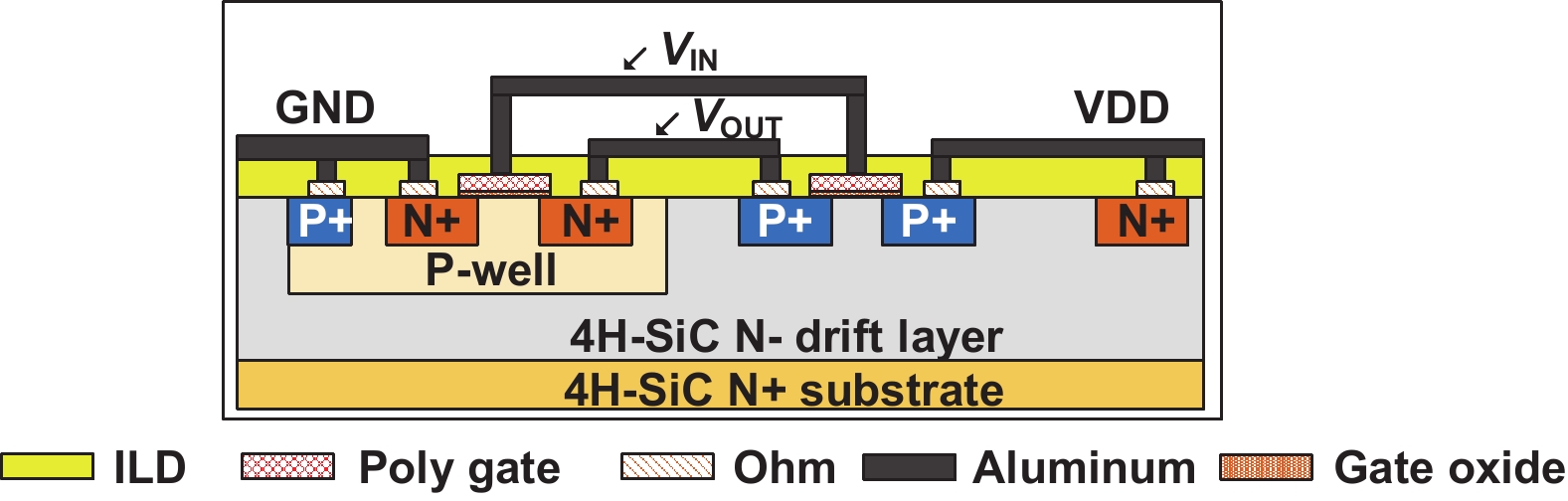
Fig. 1.
(Color online) The CMOS circuit configuration that is used in this work
ARTICLES
Tongtong Yang1, Yan Wang1, 2, and Ruifeng Yue1, 2
Corresponding author: Yan Wang, wangy46@tsinghua.edu.cn
Abstract: In this article, the design, fabrication and characterization of silicon carbide (SiC) complementary-metal-oxide-semiconductor (CMOS)-based integrated circuits (ICs) are presented. A metal interconnect strategy is proposed to fabricate the fundamental N-channel MOS (NMOS) and P-channel MOS (PMOS) devices that are required for the CMOS circuit configuration. Based on the mainstream 6-inch SiC wafer processing technology, the simultaneous fabrication of SiC CMOS ICs and power MOSFET is realized. Fundamental gates, such as inverter and NAND gates, are fabricated and tested. The measurement results show that the inverter and NAND gates function well. The calculated low-to-high delay (low-to-high output transition) and high-to-low delay (high-to-low output transition) are 49.9 and 90 ns, respectively.
Keywords: SiC, CMOS, integrated circuit, inverter, NAND, metal interconnect
| [1] |
Murphree R C, Roy S, Ahmed S, et al. A SiC CMOS linear voltage regulator for high-temperature applications. IEEE Trans Power Electron, 2020, 35, 913 doi: 10.1109/TPEL.2019.2914169
|
| [2] |
Lanni L, Malm B G, Östling M, et al. 500 °C bipolar integrated OR/NOR gate in 4H-SiC. IEEE Electron Device Lett, 2013, 34, 1091 doi: 10.1109/LED.2013.2272649
|
| [3] |
Kashyap A S, Chen C P, Ghandi R, et al. Silicon carbide integrated circuits for extreme environments. The 1st IEEE Workshop on Wide Bandgap Power Devices and Applications, 2013, 60 doi: 10.1109/WiPDA.2013.6695562
|
| [4] |
Lee J Y, Singh S, Cooper J A. Demonstration and characterization of bipolar monolithic integrated circuits in 4H-SiC. IEEE Trans Electron Devices, 2008, 55, 1946 doi: 10.1109/TED.2008.926681
|
| [5] |
Sheng K, Zhang Y X, Su M, et al. Demonstration of the first SiC power integrated circuit. Solid State Electron, 2008, 52, 1636 doi: 10.1016/j.sse.2008.06.037
|
| [6] |
Alexandru M, Banu V, Jorda X, et al. SiC integrated circuit control electronics for high-temperature operation. IEEE Trans Ind Electron, 2015, 62, 3182 doi: 10.1109/TIE.2014.2379212
|
| [7] |
Ryu S H, Kornegay K T, Cooper J A, et al. Digital CMOS IC's in 6H-SiC operating on a 5-V power supply. IEEE Trans Electron Devices, 1998, 45, 45 doi: 10.1109/16.658810
|
| [8] |
Okamoto M, Yao A, Sato H, et al. First demonstration of a monolithic SiC power IC integrating a vertical MOSFET with a CMOS gate buffer. 2021 33rd International Symposium on Power Semiconductor Devices and ICs, 2021, 71 doi: 10.23919/ISPSD50666.2021.9452262
|
| [9] |
Huang R H, Tao Y H, Bai S, et al. Design and fabrication of a 3.3 kV 4H-SiC MOSFET. J Semicond, 2015, 36, 094002 doi: 10.1088/1674-4926/36/9/094002
|
| [10] |
Licciardo G D, di Benedetto L, Bellone S. Modeling of the SiO2/SiC interface-trapped charge as a function of the surface potential in 4H-SiC vertical-DMOSFET. IEEE Trans Electron Devices, 2016, 63, 1783 doi: 10.1109/TED.2016.2531796
|
| [11] |
Yang T T, Li X B, Wang Y, et al. Design and fabrication of 860V SiC trench MOSFET with stripe and rectangular cells. 2021 IEEE International Conference on Integrated Circuits, Technologies and Applications, 2021, 161
|
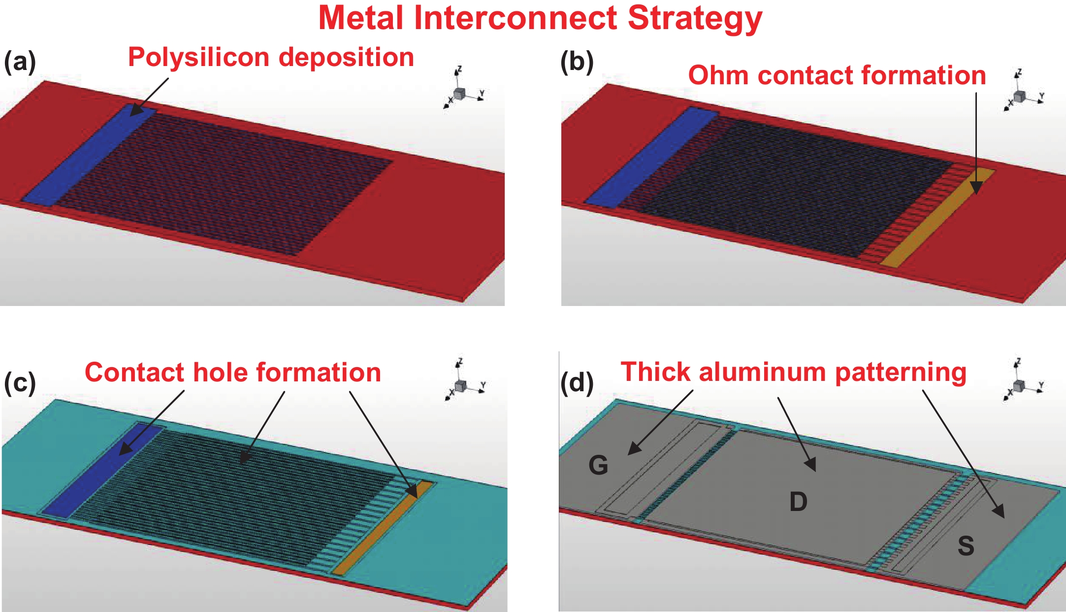
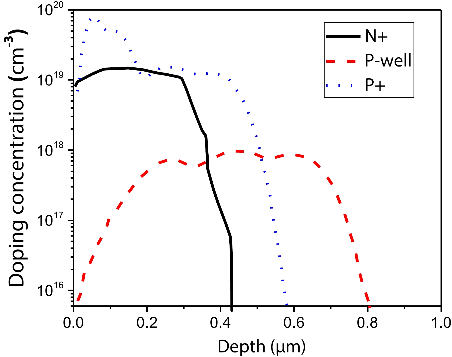
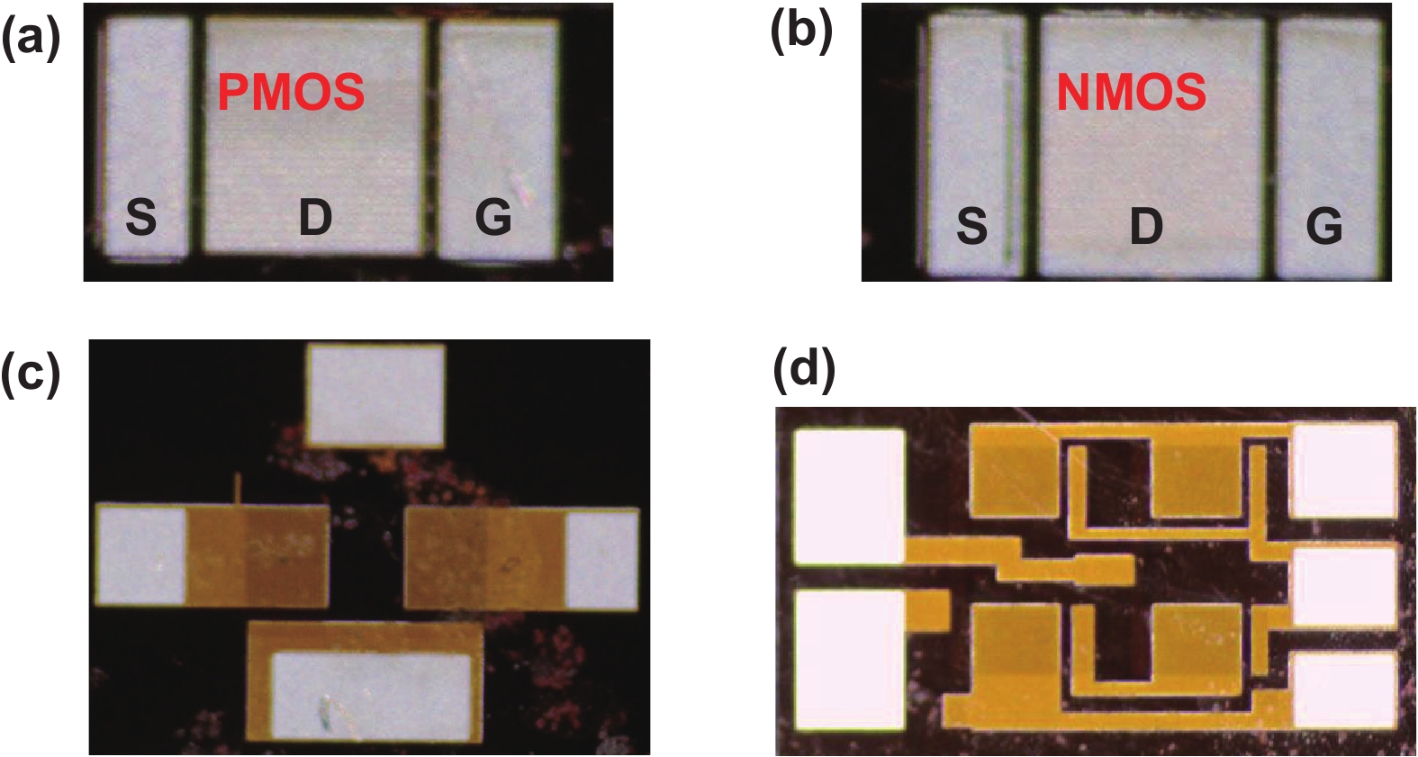
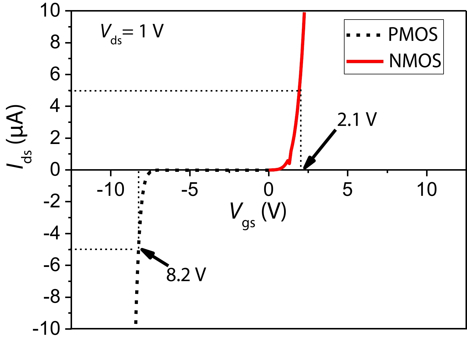
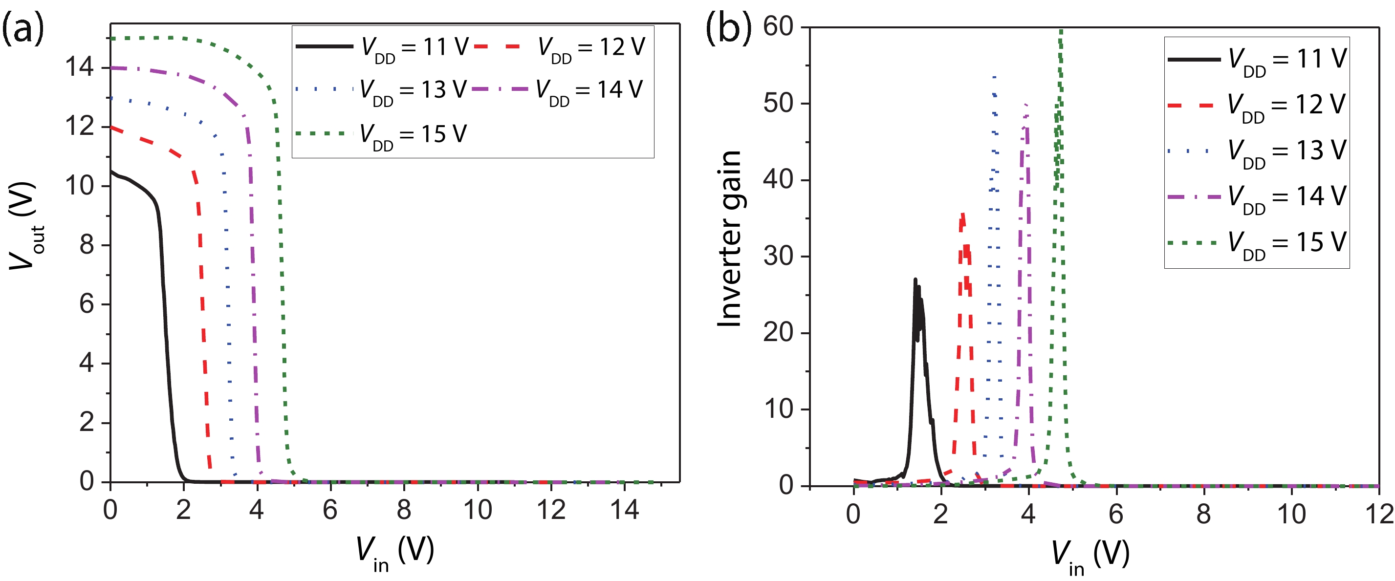
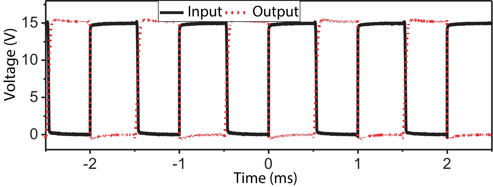
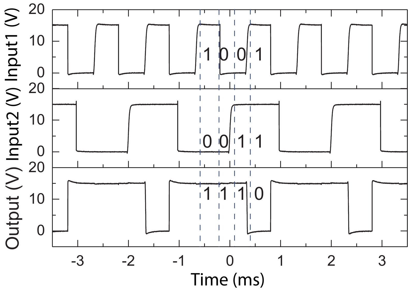
Table 1. The temperature, dose and energy used in the fabrications for P-well, P+ region and N+ regions.
| Item | Temperature (°C) | Energy (keV) |
| P-well | 500 | 550 |
| 500 | 360 | |
| 500 | 200 | |
| P+ | 500 | 320 |
| 500 | 200 | |
| 500 | 40 | |
| N+ | 500 | 160 |
| 500 | 130 | |
| 500 | 40 |
 DownLoad: CSV
| [1] |
Murphree R C, Roy S, Ahmed S, et al. A SiC CMOS linear voltage regulator for high-temperature applications. IEEE Trans Power Electron, 2020, 35, 913 doi: 10.1109/TPEL.2019.2914169
|
| [2] |
Lanni L, Malm B G, Östling M, et al. 500 °C bipolar integrated OR/NOR gate in 4H-SiC. IEEE Electron Device Lett, 2013, 34, 1091 doi: 10.1109/LED.2013.2272649
|
| [3] |
Kashyap A S, Chen C P, Ghandi R, et al. Silicon carbide integrated circuits for extreme environments. The 1st IEEE Workshop on Wide Bandgap Power Devices and Applications, 2013, 60 doi: 10.1109/WiPDA.2013.6695562
|
| [4] |
Lee J Y, Singh S, Cooper J A. Demonstration and characterization of bipolar monolithic integrated circuits in 4H-SiC. IEEE Trans Electron Devices, 2008, 55, 1946 doi: 10.1109/TED.2008.926681
|
| [5] |
Sheng K, Zhang Y X, Su M, et al. Demonstration of the first SiC power integrated circuit. Solid State Electron, 2008, 52, 1636 doi: 10.1016/j.sse.2008.06.037
|
| [6] |
Alexandru M, Banu V, Jorda X, et al. SiC integrated circuit control electronics for high-temperature operation. IEEE Trans Ind Electron, 2015, 62, 3182 doi: 10.1109/TIE.2014.2379212
|
| [7] |
Ryu S H, Kornegay K T, Cooper J A, et al. Digital CMOS IC's in 6H-SiC operating on a 5-V power supply. IEEE Trans Electron Devices, 1998, 45, 45 doi: 10.1109/16.658810
|
| [8] |
Okamoto M, Yao A, Sato H, et al. First demonstration of a monolithic SiC power IC integrating a vertical MOSFET with a CMOS gate buffer. 2021 33rd International Symposium on Power Semiconductor Devices and ICs, 2021, 71 doi: 10.23919/ISPSD50666.2021.9452262
|
| [9] |
Huang R H, Tao Y H, Bai S, et al. Design and fabrication of a 3.3 kV 4H-SiC MOSFET. J Semicond, 2015, 36, 094002 doi: 10.1088/1674-4926/36/9/094002
|
| [10] |
Licciardo G D, di Benedetto L, Bellone S. Modeling of the SiO2/SiC interface-trapped charge as a function of the surface potential in 4H-SiC vertical-DMOSFET. IEEE Trans Electron Devices, 2016, 63, 1783 doi: 10.1109/TED.2016.2531796
|
| [11] |
Yang T T, Li X B, Wang Y, et al. Design and fabrication of 860V SiC trench MOSFET with stripe and rectangular cells. 2021 IEEE International Conference on Integrated Circuits, Technologies and Applications, 2021, 161
|


Article views: 3383 Times PDF downloads: 274 Times Cited by: 0 Times
Received: 28 February 2022 Revised: 03 April 2022 Online: Accepted Manuscript: 24 May 2022Uncorrected proof: 25 May 2022Published: 01 August 2022
| Citation: |
Tongtong Yang, Yan Wang, Ruifeng Yue. Demonstration of 4H-SiC CMOS digital IC gates based on the mainstream 6-inch wafer processing technique[J]. Journal of Semiconductors, 2022, 43(8): 082801. doi: 10.1088/1674-4926/43/8/082801
****
T T Yang, Y Wang, R F Yue. Demonstration of 4H-SiC CMOS digital IC gates based on the mainstream 6-inch wafer processing technique[J]. J. Semicond, 2022, 43(8): 082801. doi: 10.1088/1674-4926/43/8/082801

|
| [1] |
Murphree R C, Roy S, Ahmed S, et al. A SiC CMOS linear voltage regulator for high-temperature applications. IEEE Trans Power Electron, 2020, 35, 913 doi: 10.1109/TPEL.2019.2914169
|
| [2] |
Lanni L, Malm B G, Östling M, et al. 500 °C bipolar integrated OR/NOR gate in 4H-SiC. IEEE Electron Device Lett, 2013, 34, 1091 doi: 10.1109/LED.2013.2272649
|
| [3] |
Kashyap A S, Chen C P, Ghandi R, et al. Silicon carbide integrated circuits for extreme environments. The 1st IEEE Workshop on Wide Bandgap Power Devices and Applications, 2013, 60 doi: 10.1109/WiPDA.2013.6695562
|
| [4] |
Lee J Y, Singh S, Cooper J A. Demonstration and characterization of bipolar monolithic integrated circuits in 4H-SiC. IEEE Trans Electron Devices, 2008, 55, 1946 doi: 10.1109/TED.2008.926681
|
| [5] |
Sheng K, Zhang Y X, Su M, et al. Demonstration of the first SiC power integrated circuit. Solid State Electron, 2008, 52, 1636 doi: 10.1016/j.sse.2008.06.037
|
| [6] |
Alexandru M, Banu V, Jorda X, et al. SiC integrated circuit control electronics for high-temperature operation. IEEE Trans Ind Electron, 2015, 62, 3182 doi: 10.1109/TIE.2014.2379212
|
| [7] |
Ryu S H, Kornegay K T, Cooper J A, et al. Digital CMOS IC's in 6H-SiC operating on a 5-V power supply. IEEE Trans Electron Devices, 1998, 45, 45 doi: 10.1109/16.658810
|
| [8] |
Okamoto M, Yao A, Sato H, et al. First demonstration of a monolithic SiC power IC integrating a vertical MOSFET with a CMOS gate buffer. 2021 33rd International Symposium on Power Semiconductor Devices and ICs, 2021, 71 doi: 10.23919/ISPSD50666.2021.9452262
|
| [9] |
Huang R H, Tao Y H, Bai S, et al. Design and fabrication of a 3.3 kV 4H-SiC MOSFET. J Semicond, 2015, 36, 094002 doi: 10.1088/1674-4926/36/9/094002
|
| [10] |
Licciardo G D, di Benedetto L, Bellone S. Modeling of the SiO2/SiC interface-trapped charge as a function of the surface potential in 4H-SiC vertical-DMOSFET. IEEE Trans Electron Devices, 2016, 63, 1783 doi: 10.1109/TED.2016.2531796
|
| [11] |
Yang T T, Li X B, Wang Y, et al. Design and fabrication of 860V SiC trench MOSFET with stripe and rectangular cells. 2021 IEEE International Conference on Integrated Circuits, Technologies and Applications, 2021, 161
|

 WeChat ID
Journal of Semiconductors © 2017 All Rights Reserved 京ICP备05085259号-2


