| [1] |
Simmons C B, Akey A J, Mailoa J P, et al. Enhancing the infrared photoresponse of silicon by controlling the fermi level location within an impurity band. Adv Funct Mater, 2014, 24(19), 2852 doi: 10.1002/adfm.201303820 |
| [2] |
Pi X D. Doping silicon nanocrystals with boron and phosphorus. J Nanomater, 2012, 2012, 3 doi: 10.1155/2012/912903 |
| [3] |
Marri I, Degoli E, Ossicini S. Doped and codoped silicon nanocrystals: The role of surfaces and interfaces. Prog Surface Sci, 2017, 92(4), 375 doi: 10.1016/j.progsurf.2017.07.003 |
| [4] |
Wang M, Debernardi A, Berencén Y, et al. Breaking the doping limit in silicon by deep impurities. Phys Rev Applied, 2019, 11, 054039 doi: 10.1103/physrevapplied.11.054039 |
| [5] |
Sánchez K, Aguilera I, Palacios P, et al. Formation of a reliable intermediate band in Si heavily coimplanted with chalcogens (S, Se, Te) and group III elements (B, Al). Phys Rev B, 2010, 82, 165201 doi: 10.1103/physrevb.82.165201 |
| [6] |
Liu F, Prucnal S, Berencén Y, et al. Realizing the insulator-to-metal transition in Se-hyperdoped Si via non-equilibrium material processing. J Phys D, 2017, 50, 415102 doi: 10.1088/1361-6463/aa82f9 |
| [7] |
Olea J, González-Díaz G, Pastor D, et al. Electronic transport properties of Ti-impurity band in Si. J Phys D, 2009, 42, 085110 doi: 10.1088/0022-3727/42/8/085110 |
| [8] |
|
| [9] |
Wang K F, Shao H Z, Liu K, et al. Possible atomic structures responsible for the sub-bandgap absorption of chalcogen-hyperdoped silicon. Appl Phys Lett, 2015, 107, 112106 doi: 10.1063/1.4931091 |
| [10] |
García-Hemme E, García-Hernansanz R, Olea J, et al. Far infrared photoconductivity in a silicon based material: Vanadium supersaturated silicon. Appl Phys Lett, 2013, 103, 032101 doi: 10.1063/1.4813823 |
| [11] |
Haberfehlner G, Smith M J, Idrobo J C, et al. Selenium segregation in femtosecond-laser hyperdoped silicon revealed by electron tomography. Microsc Microanal, 2013, 19, 716 doi: 10.1017/S1431927613000342 |
| [12] |
Luque A, Martí A, Antolín E, et al. Intermediate bands versus levels in non-radiative recombination. Phys B, 2006, 382, 320 doi: 10.1016/j.physb.2006.03.006 |
| [13] |
Wang M, Hübner R, Xu C, et al. Thermal stability of Te-hyperdoped Si: Atomic-scale correlation of the structural, electrical, and optical properties. Phys Rev Mater, 2019, 3, 044606 doi: 10.1103/physrevmaterials.3.044606 |
| [14] |
Zhou S, Pi X D, Ni Z Y, et al. Boron- and phosphorus-hyperdoped silicon nanocrystals. Part Part Syst Charact, 2015, 32, 213 doi: 10.1002/ppsc.201400103 |
| [15] |
Rowe D J, Jeong J S, Mkhoyan K A, et al. Phosphorus-doped silicon nanocrystals exhibiting mid-infrared localized surface plasmon resonance. Nano Lett, 2013, 13, 1317 doi: 10.1021/nl4001184 |
| [16] |
Wang K F, Qu S C, Liu D W, et al. Large enhancement of sub-band-gap light absorption of sulfur hyperdoped silicon by surface dome structures. Mater Lett, 2013, 107, 50 doi: 10.1016/j.matlet.2013.05.123 |
| [17] |
Sher M J, Lin Y T, Winkler M T, et al. Mid-infrared absorptance of silicon hyperdoped with chalcogen via fs-laser irradiation. J Appl Phys, 2013, 113, 063520 doi: 10.1063/1.4790808 |
| [18] |
Simmons C B, Akey A J, Krich J J, et al. Deactivation of metastable single-crystal silicon hyperdoped with sulfur. J Appl Phys, 2013, 114, 243514 doi: 10.1063/1.4854835 |
| [19] |
Yang W, Ferdous N, Simpson P J, et al. Evidence for vacancy trapping in Au-hyperdoped Si following pulsed laser melting. APL Mater, 2019, 7, 101124 doi: 10.1063/1.5124709 |
| [20] |
Bao J M, Tabbal M, Kim T, et al. Point defect engineered Si sub-bandgap light-emitting diode. Opt Express, 2007, 15, 6727 doi: 10.1364/oe.15.006727 |
| [21] |
Carey P G, Bezjian K, Sigmon T W, et al. Fabrication of submicrometer MOSFET's using gas immersion laser doping (GILD). IEEE Electron Device Lett, 1986, 7, 440 doi: 10.1109/EDL.1986.26429 |
| [22] |
Wen C, Shi Z Q, Wang Z J, et al. Zinc-hyperdoped silicon nanocrystalline layers prepared via nanosecond laser melting for broad light absorption. Opt Laser Technol, 2021, 144, 107415 doi: 10.1016/j.optlastec.2021.107415 |
| [23] |
Komarov F F, Nechaev N S, Ivlev G D, et al. Structural and optical properties of Si hyperdoped with Te by ion implantation and pulsed laser annealing. Vacuum, 2020, 178, 109434 doi: 10.1016/j.vacuum.2020.109434 |
| [24] |
|
| [25] |
Kik P G, Polman A, Libertino S, et al. Design and performance of an erbium-doped silicon waveguide detector operating at 1.5 µm. J Light Technol, 2002, 20, 862 doi: 10.1109/JLT.2002.1007941 |
| [26] |
Zhao X Y, Lin K M, Gao S, et al. Efficient Er/O doped silicon photodiodes at communication wavelengths by deep cooling. Adv Mater Technol, 2021, 2100137 doi: 10.1002/admt.202100137 |
| [27] |
Mailoa J P, Akey A J, Simmons C B, et al. Room-temperature sub-band gap optoelectronic response of hyperdoped silicon. Nat Commun, 2014, 5, 1 doi: 10.1038/ncomms4011 |
| [28] |
Recht D, Sullivan J T, Reedy R, et al. Controlling dopant profiles in hyperdoped silicon by modifying dopant evaporation rates during pulsed laser melting. Appl Phys Lett, 2012, 100, 112112 doi: 10.1063/1.3695171 |
| [29] |
Li S J, Han P D. Effects of high temperature annealing and laser irradiation on activation rate of phosphorus. J Semicond, 2020, 41, 122701 doi: 10.1088/1674-4926/41/12/122701 |
| [30] |
Bob B P, Kohno A, Charnvanichborikarn S, et al. Fabrication and subband gap optical properties of silicon supersaturated with chalcogens by ion implantation and pulsed laser melting. J Appl Phys, 2010, 107, 123506 doi: 10.1063/1.3415544 |
| [31] |
Yang W, Hudspeth Q, Chow P K, et al. Atomistic mechanisms for the thermal relaxation of Au-hyperdoped Si. Phys Rev Appl, 2019, 12, 024015 doi: 10.1103/physrevapplied.12.024015 |
| [32] |
Lim S Q, Lew C T K, Chow P K, et al. Toward understanding and optimizing Au-hyperdoped Si infrared photodetectors. APL Mater, 2020, 8, 061109 doi: 10.1063/5.0010083 |
| [33] |
Lim S Q, Akey A J, Napolitani E, et al. A critical evaluation of Ag- and Ti-hyperdoped Si for Si-based infrared light detection. J Appl Phys, 2021, 129, 065701 doi: 10.1063/5.0035620 |
| [34] |
Prucnal S, Rebohle L, Skorupa W. Doping by flash lamp annealing. Mater Sci Semicond Process, 2017, 62, 115 doi: 10.1016/j.mssp.2016.10.040 |
| [35] |
Berencén Y, Prucnal S, Liu F, et al. Room-temperature short-wavelength infrared Si photodetector. Sci Rep, 2017, 7, 43688 doi: 10.1038/srep43688 |
| [36] |
McMahon R A, Smith M P, Seffen K A, et al. Flash-lamp annealing of semiconductor materials—Applications and process models. Vacuum, 2007, 81, 1301 doi: 10.1016/j.vacuum.2007.01.033 |
| [37] |
Zhou S Q, Liu F, Prucnal S, et al. Hyperdoping silicon with selenium: Solid vs. liquid phase epitaxy. Sci Rep, 2015, 5, 8329 doi: 10.1038/srep08329 |
| [38] |
Wang M, Yu Y, Prucnal S, et al. Mid- and far-infrared localized surface plasmon resonances in chalcogen-hyperdoped silicon. Nanoscale, 2022, 14, 2826 doi: 10.1039/D1NR07274A |
| [39] |
Wang K, Gao J S, Yang H G, et al. Study on top sulfur hyperdoping layer covering microstructured Si by fs-laser irradiation. Appl Surf Sci, 2019, 464, 502 doi: 10.1016/j.apsusc.2018.09.125 |
| [40] |
Pan S H, Recht D, Charnvanichborikarn S, et al. Enhanced visible and near-infrared optical absorption in silicon supersaturated with chalcogens. Appl Phys Lett, 2011, 98, 121913 doi: 10.1063/1.3567759 |
| [41] |
Sun H B, Liu X L, Zhao L, et al. Mid-long wavelength infrared absorptance of hyperdoped silicon via femtosecond laser microstructuring. Opt Express, 2022, 30, 1808 doi: 10.1364/oe.446283 |
| [42] |
Limaye M V, Chen S C, Lee C Y, et al. Understanding of sub-band gap absorption of femtosecond-laser sulfur hyperdoped silicon using synchrotron-based techniques. Sci Rep, 2015, 5, 11466 doi: 10.1038/srep11466 |
| [43] |
Carey J E, Crouch C H, Shen M Y, et al. Visible and near-infrared responsivity of femtosecond-laser microstructured silicon photodiodes. Opt Lett, 2005, 30, 1773 doi: 10.1364/OL.30.001773 |
| [44] |
Gimpel T, Höger I, Falk F, et al. Electron backscatter diffraction on femtosecond laser sulfur hyperdoped silicon. Appl Phys Lett, 2012, 101, 111911 doi: 10.1063/1.4752454 |
| [45] |
Warrender J M. Laser hyperdoping silicon for enhanced infrared optoelectronic properties. Appl Phys Rev, 2016, 3, 031104 doi: 10.1063/1.4960752 |
| [46] |
Crouch C H, Carey J E, Shen M, et al. Infrared absorption by sulfur-doped silicon formed by femtosecond laser irradiation. Appl Phys A, 2004, 79, 1635 doi: 10.1007/s00339-004-2676-0 |
| [47] |
Smith M J, Lin Y T, Sher M J, et al. Pressure-induced phase transformations during femtosecond-laser doping of silicon. J Appl Phys, 2011, 110, 053524 doi: 10.1063/1.3633528 |
| [48] |
Gimpel T, Guenther K M, Kontermann S, et al. Current-voltage characteristic and sheet resistances after annealing of femtosecond laser processed sulfur emitters for silicon solar cells. Appl Phys Lett, 2014, 105, 053504 doi: 10.1063/1.4892474 |
| [49] |
Sundaram S K, Mazur E. Inducing and probing non-thermal transitions in semiconductors using femtosecond laser pulses. Nat Mater, 2002, 1, 217 doi: 10.1038/nmat767 |
| [50] |
Crouch C H, Carey J E, Warrender J M, et al. Comparison of structure and properties of femtosecond and nanosecond laser-structured silicon. Appl Phys Lett, 2004, 84, 1850 doi: 10.1063/1.1667004 |
| [51] |
Franta B, Pastor D, Gandhi H H, et al. Simultaneous high crystallinity and sub-bandgap optical absorptance in hyperdoped black silicon using nanosecond laser annealing. J Appl Phys, 2015, 118, 225303 doi: 10.1063/1.4937149 |
| [52] |
Olea J, Toledano-Luque M, Pastor D, et al. High quality Ti-implanted Si layers above the Mott limit. J Appl Phys, 2010, 107, 103524 doi: 10.1063/1.3391274 |
| [53] |
Umezu I, Naito M, Kawabe D, et al. Hyperdoping of silicon with deep-level impurities by pulsed YAG laser melting. Appl Phys A, 2014, 117, 155 doi: 10.1007/s00339-014-8313-7 |
| [54] |
Zhang Y B, Li X H, Lin X M, et al. Negative photoconductivity in sulfur-hyperdoped silicon film. Mater Sci Semicond Process, 2019, 98, 106 doi: 10.1016/j.mssp.2019.04.002 |
| [55] |
Carey P G, Sigmon T W. In-situ doping of silicon using the gas immersion laser doping (GILD) process. Appl Surf Sci, 1989, 43, 325 doi: 10.1016/0169-4332(89)90234-1 |
| [56] |
Hoummada K, Dahlem F, Kociniewski T, et al. Absence of boron aggregates in superconducting silicon confirmed by atom probe tomography. Appl Phys Lett, 2012, 101, 182602 doi: 10.1063/1.4760261 |
| [57] |
Sher M J, Mazur E. Intermediate band conduction in femtosecond-laser hyperdoped silicon. Appl Phys Lett, 2014, 105, 032103 doi: 10.1063/1.4890618 |
| [58] |
Sher M J, Simmons C B, Krich J J, et al. Picosecond carrier recombination dynamics in chalcogen-hyperdoped silicon. Appl Phys Lett, 2014, 105, 053905 doi: 10.1063/1.4892357 |
| [59] |
Meng-Ju S, Mangan N M, Smith M J, et al. Femtosecond-laser hyperdoping silicon in an SF 6 atmosphere: Dopant incorporation mechanism. J Appl Phys, 2015, 117, 125301 doi: 10.1063/1.4914520 |
| [60] |
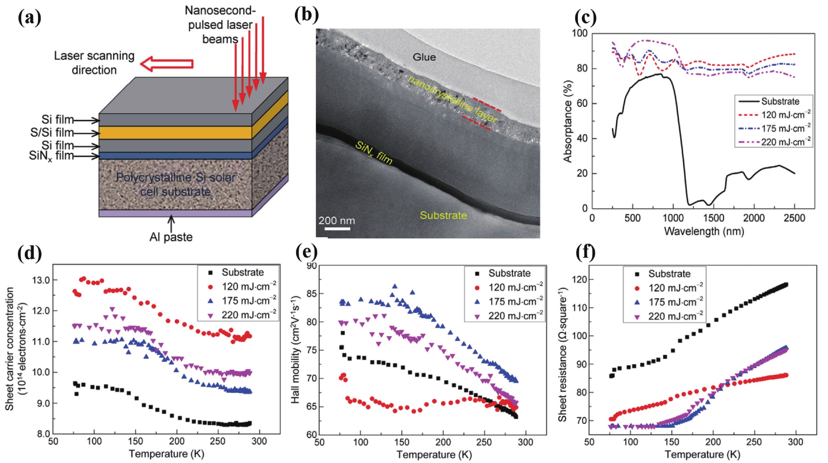
|
| [61] |
Dong X, Li N, Zhu Z, et al. A nitrogen-hyperdoped silicon material formed by femtosecond laser irradiation. Appl Phys Lett, 2014, 104, 091907 doi: 10.1063/1.4868017 |
| [62] |
Alpass C R, Murphy J D, Falster R J, et al. Nitrogen diffusion and interaction with dislocations in single-crystal silicon. J Appl Phys, 2009, 105, 013519 doi: 10.1063/1.3050342 |
| [63] |
Dong X, Wang Y Y, Song X H. Engineering intermediate-band photovoltaic material by heavily co-doping selenium and nitrogen in silicon. Appl Phys Express, 2018, 11, 011303 doi: 10.7567/apex.11.011303 |
| [64] |
Dong X, Wang Y Y, Song X H, et al. First-principles studies of a photovoltaic material based on silicon heavily codoped with sulfur and nitrogen. Appl Phys Express, 2018, 11, 031303 doi: 10.7567/apex.11.031303 |
| [65] |
Lin Y T, Mangan N, Marbach S, et al. Creating femtosecond-laser-hyperdoped silicon with a homogeneous doping profile. Appl Phys Lett, 2015, 106, 062105 doi: 10.1063/1.4907988 |
| [66] |
Newman B K, Ertekin E, Sullivan J T, et al. Extended X-ray absorption fine structure spectroscopy of selenium-hyperdoped silicon. J Appl Phys, 2013, 114, 133507 doi: 10.1063/1.4824279 |
| [67] |
Jia Z X, Wu Q, Jin X R, et al. Highly responsive tellurium-hyperdoped black silicon photodiode with single-crystalline and uniform surface microstructure. Opt Express, 2020, 28, 5239 doi: 10.1364/OE.385887 |
| [68] |
Du L Y, Wu Z M, Li R, et al. Near-infrared photoresponse of femtosecond-laser processed Se-doped silicon n +-n photodiodes. Opt Lett, 2016, 41, 5031 doi: 10.1364/OL.41.005031 |
| [69] |
Yu X Y, Zhao J H, Li C H, et al. Gold-hyperdoped black silicon with high IR absorption by femtosecond laser irradiation. IEEE Trans Nanotechnol, 2017, 16, 502 doi: 10.1109/TNANO.2017.2693691 |
| [70] |
Qiu X D, Yu X G, Yuan S, et al. Trap assisted bulk silicon photodetector with high photoconductive gain, low noise, and fast response by Ag hyperdoping. Adv Opt Mater, 2018, 6, 1700638 doi: 10.1002/adom.201700638 |
| [71] |
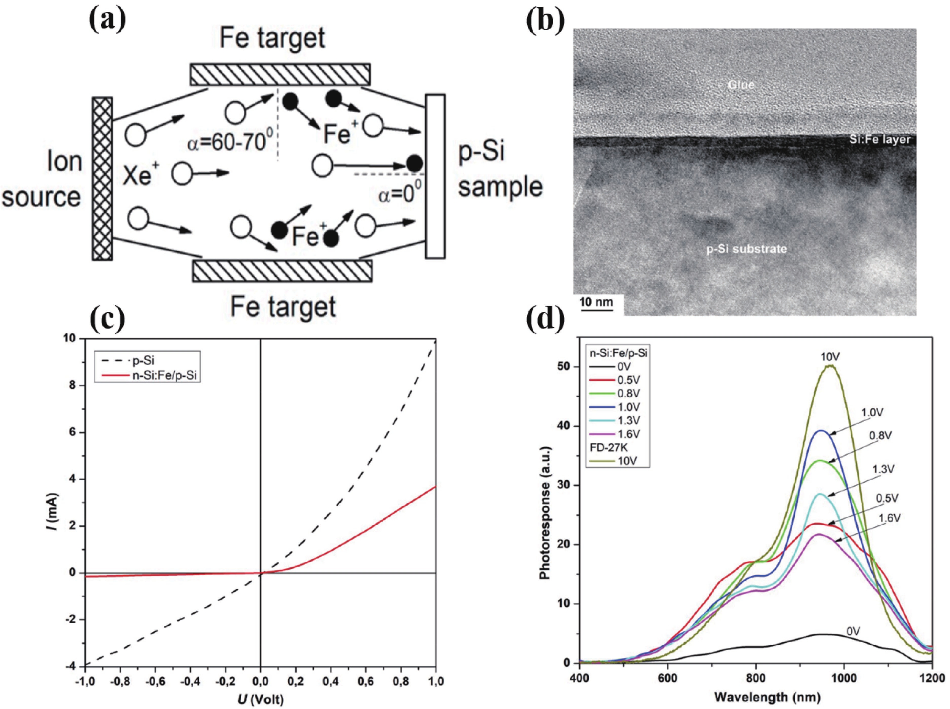
Batalov R, Bayazitov R, Faizrakhmanov I, et al. Photoelectric and magnetic properties of Fe-hyperdoped Si layers formed by the recoil-atom implantation. Mater Sci Semicond Process, 2020, 105, 104752 doi: 10.1016/j.mssp.2019.104752 |
| [72] |
Chen R, Fan B D, Pan M, et al. Room-temperature optoelectronic response of Ni supersaturated p-type Si processed by continuous-wave laser irradiation. Mater Lett, 2016, 163, 90 doi: 10.1016/j.matlet.2015.10.018 |
| [73] |
Istratov A A, Zhang P, McDonald R J, et al. Nickel solubility in intrinsic and doped silicon. J Appl Phys, 2005, 97, 023505 doi: 10.1063/1.1836852 |
| [74] |
Luan Q B, Ni Z Y, Koura S, et al. Low-resistivity bulk silicon prepared by hot-pressing boron- and phosphorus-hyperdoped silicon nanocrystals. AIP Adv, 2014, 4, 127108 doi: 10.1063/1.4903550 |
| [75] |
Chen J J, Rohani P, Karakalos S G, et al. Boron-hyperdoped silicon for the selective oxidative dehydrogenation of propane to propylene. Chem Commun, 2020, 56, 9882 doi: 10.1039/D0CC02822C |
| [76] |
Moutanabbir O, Isheim D, Blumtritt H, et al. Colossal injection of catalyst atoms into silicon nanowires. Nature, 2013, 496, 78 doi: 10.1038/nature11999 |
| [77] |
Zhou Z P, Yin B, Michel J. On-chip light sources for silicon photonics. Light Sci Appl, 2015, 4, e358 doi: 10.1038/lsa.2015.131 |
| [78] |
Polman A. Erbium implanted thin film photonic materials. J Appl Phys, 1997, 82, 1 doi: 10.1063/1.366265 |
| [79] |
Wen H M, He J J, Hong J, et al. Efficient Er/O-doped silicon light-emitting diodes at communication wavelength by deep cooling. Adv Opt Mater, 2020, 8, 2000720 doi: 10.1002/adom.202000720 |
| [80] |
Bustarret E, Marcenat C, Achatz P, et al. Superconductivity in doped cubic silicon. Nature, 2006, 444, 465 doi: 10.1038/nature05340 |
| [81] |
Boeri L, Kortus J, Andersen O K. Three-dimensional MgB 2-type superconductivity in hole-doped diamond. Phys Rev Lett, 2004, 93, 237002 doi: 10.1103/PhysRevLett.93.237002 |
| [82] |
Ertekin E, Winkler M T, Recht D, et al. Insulator-to-metal transition in selenium-hyperdoped silicon: Observation and origin. Phys Rev Lett, 2012, 108, 026401 doi: 10.1103/PhysRevLett.108.026401 |
| [83] |
Yang W J, Mathews J, Williams J S. Hyperdoping of Si by ion implantation and pulsed laser melting. Mater Sci Semicond Process, 2017, 62, 103 doi: 10.1016/j.mssp.2016.11.005 |
| [84] |
Sullivan J T, Simmons C B, Krich J J, et al. Methodology for vetting heavily doped semiconductors for intermediate band photovoltaics: A case study in sulfur-hyperdoped silicon. J Appl Phys, 2013, 114, 103701 doi: 10.1063/1.4820454 |
| [85] |
Sheehy M A, Tull B R, Friend C M, et al. Chalcogen doping of silicon via intense femtosecond-laser irradiation. Mater Sci Eng B, 2007, 137, 289 doi: 10.1016/j.mseb.2006.10.002 |
| [86] |
Recht D, Hutchinson D, Cruson T, et al. Contactless microwave measurements of photoconductivity in silicon hyperdoped with chalcogens. Appl Phys Express, 2012, 5, 041301 doi: 10.1143/apex.5.041301 |
| [87] |
Krich J J, Halperin B I, Aspuru-Guzik A. Nonradiative lifetimes in intermediate band photovoltaics—Absence of lifetime recovery. J Appl Phys, 2012, 112, 013707 doi: 10.1063/1.4732085 |
| [88] |
Sullivan J T, Simmons C B, Buonassisi T, et al. Targeted search for effective intermediate band solar cell materials. IEEE J Photovolt, 2015, 5, 212 doi: 10.1109/JPHOTOV.2014.2363560 |
| [89] |
Li X Y, Han P D, Gao L P, et al. Electronic properties investigation of silicon supersaturated with tellurium. Appl Phys A, 2011, 105, 1021 doi: 10.1007/s00339-011-6537-3 |
| [90] |
Zhou Y R, Liu F Z, Song X H. The insulator-to-metal transition of Co hyperdoped crystalline silicon. J Appl Phys, 2013, 113, 103702 doi: 10.1063/1.4794818 |
| [91] |
|
| [92] |
Dong X, Fang X X, Wang Y Y, et al. Modulating the band structure and sub-bandgap absorption of Co-hyperdoped silicon by co-doping with shallow-level elements. Appl Phys Express, 2018, 11, 061301 doi: 10.7567/apex.11.061301 |
| [93] |
Dong X, Song X H, Wang Y Y, et al. First-principles calculations of a promising intermediate-band photovoltaic material based on Co-hyperdoped crystalline silicon. Appl Phys Express, 2015, 8, 081302 doi: 10.7567/apex.8.081302 |
| [94] |
Olea J, del Prado A, Pastor D, et al. Sub-bandgap absorption in Ti implanted Si over the Mott limit. J Appl Phys, 2011, 109, 113541 doi: 10.1063/1.3596525 |
| [95] |
Tull B R, Winkler M T, Mazur E. The role of diffusion in broadband infrared absorption in chalcogen-doped silicon. Appl Phys A, 2009, 96, 327 doi: 10.1007/s00339-009-5200-8 |
| [96] |
Newman B K, Sher M J, Mazur E, et al. Reactivation of sub-bandgap absorption in chalcogen-hyperdoped silicon. Appl Phys Lett, 2011, 98, 251905 doi: 10.1063/1.3599450 |
| [97] |
Wen C, Chen W, Chen Y P, et al. Thermal annealing performance of sulfur-hyperdoped black silicon fabricated using a Nd: YAG nanosecond-pulsed laser. Mater Res Bull, 2017, 93, 238 doi: 10.1016/j.materresbull.2017.05.011 |
| [98] |
Wang K F, Liu P G, Qu S C, et al. Optical and electrical properties of textured sulfur-hyperdoped silicon: A thermal annealing study. J Mater Sci, 2015, 50, 3391 doi: 10.1007/s10853-015-8895-2 |
| [99] |
Zhou S, Ni Z Y, Ding Y, et al. Ligand-free, colloidal, and plasmonic silicon nanocrystals heavily doped with boron. ACS Photonics, 2016, 3, 415 doi: 10.1021/acsphotonics.5b00568 |
| [100] |
Slotboom J W, de Graaff H C. Measurements of bandgap narrowing in Si bipolar transistors. Solid State Electron, 1976, 19, 857 doi: 10.1016/0038-1101(76)90043-5 |
| [101] |
Pi X D, Delerue C. Tight-binding calculations of the optical response of optimally P-doped Si nanocrystals: A model for localized surface plasmon resonance. Phys Rev Lett, 2013, 111, 177402 doi: 10.1103/physrevlett.111.177402 |
| [102] |
Ni Z Y, Pi X D, Zhou S, et al. Size-dependent structures and optical absorption of boron-hyperdoped silicon nanocrystals. Adv Opt Mater, 2016, 4, 700 doi: 10.1002/adom.201500706 |
| [103] |
Rohani P, Banerjee S, Sharifi-Asl S, et al. Synthesis and properties of plasmonic boron-hyperdoped silicon nanoparticles. Adv Funct Mater, 2019, 29, 1807788 doi: 10.1002/adfm.201807788 |
| [104] |
Beard M C, Luther J M, Nozik A J. The promise and challenge of nanostructured solar cells. Nat Nanotechnol, 2014, 9, 951 doi: 10.1038/nnano.2014.292 |
| [105] |
Cui Y, Lieber C M. Functional nanoscale electronic devices assembled using silicon nanowire building blocks. Science, 2001, 291, 851 doi: 10.1126/science.291.5505.851 |
| [106] |
Tian B Z, Zheng X L, Kempa T J, et al. Coaxial silicon nanowires as solar cells and nanoelectronic power sources. Nature, 2007, 449, 885 doi: 10.1038/nature06181 |
| [107] |
|
| [108] |
Li L Y, Cheng Y F, Liu Z Y, et al. Study of structure-property relationship of semiconductor nanomaterials by off-axis electron holography. J Semicond, 2022, 43, 041103 doi: 10.1088/1674-4926/43/4/041103 |
| [109] |
Berencén Y, Prucnal S, Möller W, et al. CMOS-compatible controlled hyperdoping of silicon nanowires. Adv Mater Interfaces, 2018, 5, 1800101 doi: 10.1002/admi.201800101 |
| [110] |
Ke Y, Weng X J, Redwing J M, et al. Fabrication and electrical properties of si nanowires synthesized by Al catalyzed vapor-liquid-solid growth. Nano Lett, 2009, 9, 4494 doi: 10.1021/nl902808r |
| [111] |
Chang C B, Tsai C Y, Chen K T, et al. Solution-grown phosphorus-hyperdoped silicon nanowires/carbon nanotube bilayer fabric as a high-performance lithium-ion battery anode. ACS Appl Energy Mater, 2021, 4, 3160 doi: 10.1021/acsaem.0c02932 |
| [112] |
Tanaka Y, Furata M, Mastuura H, et al. Development of high-sensitive gas-sensor for B 2H 6 using gas-permeable conductive DLC membrane. ECS Trans, 2008, 16, 387 doi: 10.1149/1.2981143 |
| [113] |
Narducci D, Zulian L, Lorenzi B, et al. Exceptional thermoelectric power factors in hyperdoped, fully dehydrogenated nanocrystalline silicon thin films. Appl Phys Lett, 2021, 119, 263903 doi: 10.1063/5.0076547 |
| [114] |
Yanagisawa R, Tsujii N, Mori T K, et al. Nanostructured planar-type uni-leg Si thermoelectric generators. Appl Phys Express, 2020, 13, 095001 doi: 10.35848/1882-0786/aba5c4 |
| [115] |
Kondrotas R, Chen C, Liu X X, et al. Low-dimensional materials for photovoltaic application. J Semicond, 2021, 42, 031701 doi: 10.1088/1674-4926/42/3/031701 |
| [116] |
Zhu Y Y, Zhang Q P, Shu L, et al. Recent progress of efficient flexible solar cells based on nanostructures. J Semicond, 2021, 42, 101604 doi: 10.1088/1674-4926/42/10/101604 |
| [117] |
Wang K, Li X H, Zhang Y B, et al. Study of titanium-doped silicon films prepared by magnetron sputtering and nanosecond pulsed laser. Acta Photonica Sinic, 2018, 47, 916005 doi: 10.3788/gzxb20184709.0916005 |
| [118] |
Hocine S, Mathiot D. Titanium diffusion in silicon. Appl Phys Lett, 1988, 53, 1269 doi: 10.1063/1.100446 |
| [119] |
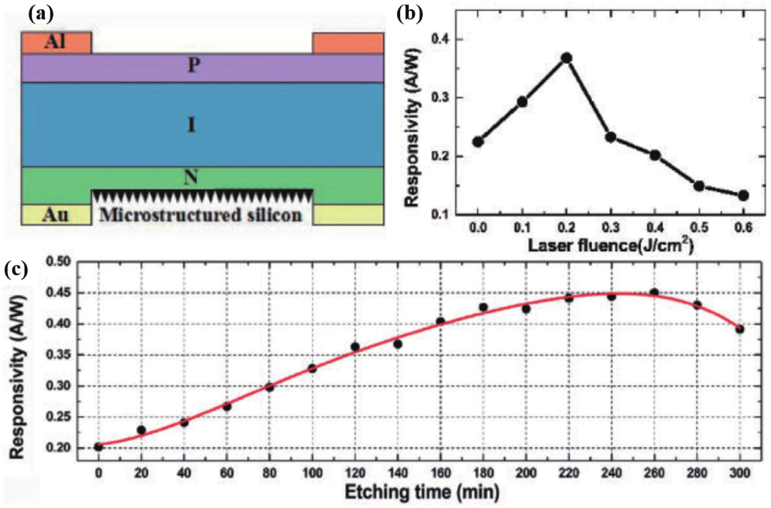
Wen C, Yang Y J, Ma Y J, et al. Sulfur-hyperdoped silicon nanocrystalline layer prepared on polycrystalline silicon solar cell substrate by thin film deposition and nanosecond-pulsed laser irradiation. Appl Surf Sci, 2019, 476, 49 doi: 10.1016/j.apsusc.2019.01.074 |
| [120] |
Saring P, Lena Baumann A, Schlieper-Ludewig B, et al. Electronic and structural properties of femtosecond laser sulfur hyperdoped silicon pn-junctions. Appl Phys Lett, 2013, 103, 061904 doi: 10.1063/1.4817726 |
| [121] |
Umezu I, Warrender J M, Charnvanichborikarn S, et al. Emergence of very broad infrared absorption band by hyperdoping of silicon with chalcogens. J Appl Phys, 2013, 113, 213501 doi: 10.1063/1.4804935 |
| [122] |
Zhang T, Ahmad W, Liu B H, et al. Broadband infrared response of sulfur hyperdoped silicon under femtosecond laser irradiation. Mater Lett, 2017, 196, 16 doi: 10.1016/j.matlet.2017.03.011 |
| [123] |
Chiodi F, Grockowiak A, Duvauchelle J E, et al. Gas immersion laser doping for superconducting nanodevices. Appl Surf Sci, 2014, 302, 209 doi: 10.1016/j.apsusc.2013.10.101 |
| [124] |
Sardashti K, Nguyen T, Hatefipour M, et al. Tailoring superconducting phases observed in hyperdoped Si:Ga for cryogenic circuit applications. Appl Phys Lett, 2021, 118, 073102 doi: 10.1063/5.0039983 |
| [125] |
Liu X L, Zhao Y, Ma S X, et al. Rapid and wide-range detection of NO x gas by N-hyperdoped silicon with the assistance of a photovoltaic self-powered sensing mode. ACS Sens, 2019, 4, 3056 doi: 10.1021/acssensors.9b01704 |
| [126] |
Zhu Z, Shao H Z, Dong X, et al. Electronic band structure and sub-band-gap absorption of nitrogen hyperdoped silicon. Sci Rep, 2015, 5, 10513 doi: 10.1038/srep10513 |
| [127] |
Dong X, Wang Y Y, Song X H. Calculational Raman spectra investigation of nitrogen-hyperdoped silicon formed in different conditions. J Phys Condens Matter, 2020, 32, 115701 doi: 10.1088/1361-648X/ab5901 |
| [128] |
Zhao Z Y, Yang P Z. Insight into insulator-to-metal transition of sulfur-doped silicon by DFT calculations. Phys Chem Chem Phys, 2014, 16, 17499 doi: 10.1039/C4CP01522C |
| [129] |
Qiu X D, Wang Z J, Hou X T, et al. Visible-blind short-wavelength infrared photodetector with high responsivity based on hyperdoped silicon. Photonics Res, 2019, 7, 351 doi: 10.1364/PRJ.7.000351 |
| [130] |
Li C H, Wang X P, Zhao J H, et al. Black silicon IR photodiode supersaturated with nitrogen by femtosecond laser irradiation. IEEE Sens J, 2018, 18, 3595 doi: 10.1109/JSEN.2018.2812730 |
| [131] |
Wang K, Yang H G, Wang X Y, et al. 1064 nm photoresponse enhancement of femtosecond-laser-irradiated Si photodiodes by etching treatment. Appl Phys Express, 2018, 11, 062203 doi: 10.7567/apex.11.062203 |
| [132] |
Zhang T, Liu B H, Ahmad W, et al. Optical and electronic properties of femtosecond laser-induced sulfur-hyperdoped silicon N+/P photodiodes. Nanoscale Res Lett, 2017, 12, 522 doi: 10.1186/s11671-017-2287-2 |
| [133] |
García Hemme E, Garcia-Hernansanz R, Olea J, et al. Room-temperature operation of a titanium supersaturated silicon-based infrared photodetector. Appl Phys Lett, 2014, 104, 211105 doi: 10.1063/1.4879851 |
| [134] |
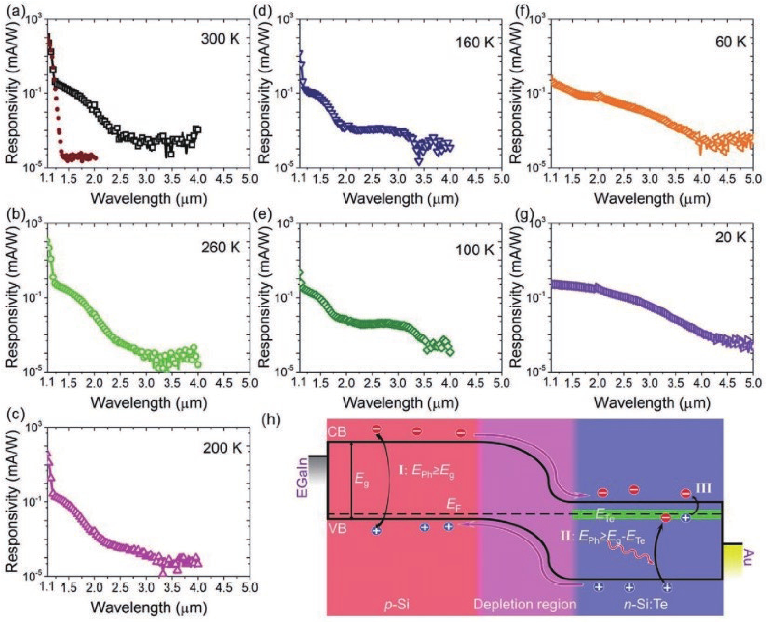
Wang M, Berencén Y, García-Hemme E, et al. Extended infrared photoresponse in Te-HyperdopedSi at room temperature. Phys Rev Appl, 2018, 10, 024054 doi: 10.1103/physrevapplied.10.024054 |
| [135] |
Wang M, García-Hemme E, Berencén Y, et al. Silicon-based intermediate-band infrared photodetector realized by Te hyperdoping. Adv Optical Mater, 2021, 9, 2101798 doi: 10.1002/adom.202001546 |
| [136] |
Sheehy M A. Femtosecond-laser microstructuring of silicon: Dopants and defects. Harvard University, 2004
|
| [137] |
Cagnina S F. Enhanced gold solubility effect in heavily n-type silicon. J Electrochem Soc, 1969, 116, 498 doi: 10.1149/1.2411921 |
| [138] |
García Hemme E, Garcia-Hernansanz R, Olea J, et al. Double ion implantation and pulsed laser melting processes for third generation solar cells. Int J Photoenergy, 2013, 2013, 1 doi: 10.1155/2013/473196 |
| [139] |
Hu S X, Han P D, Liang P, et al. Metallic conduction behavior in selenium-hyperdoped silicon. Mater Sci Semicond Process, 2014, 17, 134 doi: 10.1016/j.mssp.2013.09.001 |
| [140] |
Gimpel T, Guenther K M, Kontermann S, et al. Study on contact materials for sulfur hyperdoped black silicon. 2011 37th IEEE Photovoltaic Specialists Conference, 2011, 2061 doi: 10.1109/PVSC.2011.6186358 |
| [141] |
Gimpel T, Winter S, Boßmeyer M, et al. Quantum efficiency of femtosecond-laser sulfur hyperdoped silicon solar cells after different annealing regimes. Sol Energy Mater Sol Cells, 2018, 180, 168 doi: 10.1016/j.solmat.2018.03.001 |
| [142] |
Cammilleri D, Fossard F, Débarre D, et al. Highly doped Si and Ge formed by GILD (gas immersion laser doping); from GILD to superconducting silicon. Thin Solid Films, 2008, 517, 75 doi: 10.1016/j.tsf.2008.08.073 |
| [143] |
Grockowiak A, Klein T, Cercellier H, et al. Thickness dependence of the superconducting critical temperature in heavily doped Si: B epilayers. Phys Rev B, 2013, 88, 064508 doi: 10.1103/physrevb.88.064508 |
| [144] |
Grockowiak A, Klein T, Bustarret E, et al. Superconducting properties of laser annealed implanted Si:B epilayers. Supercond Sci Technol, 2013, 26, 045009 doi: 10.1088/0953-2048/26/4/045009 |
| [145] |
Liu X L, Zhu S W, Sun H B, et al. “Infinite sensitivity” of black silicon ammonia sensor achieved by optical and electric dual drives. ACS Appl Mater Interfaces, 2018, 10, 5061 doi: 10.1021/acsami.7b16542 |
| [146] |
Zhao Y, Liu X L, Ma S X, et al. Light-optimized photovoltaic self-powered NO 2 gas sensing based on black silicon. Sens Actuat B, 2021, 340, 129985 doi: 10.1016/j.snb.2021.129985 |
| [147] |
Wang W J, Ma S X, Liu X L, et al. NO 2 gas sensor with excellent performance based on thermally modified nitrogen-hyperdoped silicon. Sens Actuat B, 2022, 354, 131193 doi: 10.1016/j.snb.2021.131193 |


 DownLoad: