


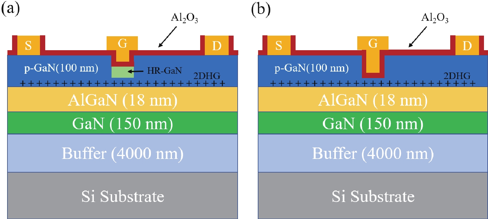
Fig. 1.
(Color online) Schematic of pFETs on the p-GaN gate power HEMT platform. (a) Device A; (b) device B.
ARTICLES
Xiaotian Gao1, Guohao Yu2, 3, Jiaan Zhou2, Zheming Wang2, Yu Li2, Jijun Zhang1, Xiaoyan Liang1, Zhongming Zeng2 and Baoshun Zhang2, 3,
Corresponding author: Baoshun Zhang, bszhang2006@sinano.ac.cn
Abstract: This letter showcases the successful fabrication of an enhancement-mode (E-mode) buried p-channel GaN field-effect-transistor on a standard p-GaN/AlGaN/GaN-on-Si power HEMT substrate. The transistor exhibits a threshold voltage (VTH) of −3.8 V, a maximum ON-state current (ION) of 1.12 mA/mm, and an impressive ION/IOFF ratio of 107. To achieve these remarkable results, an H plasma treatment was strategically applied to the gated p-GaN region, where a relatively thick GaN layer (i.e., 70 nm) was kept intact without aggressive gate recess. Through this treatment, the top portion of the GaN layer was converted to be hole-free, leaving only the bottom portion p-type and spatially separated from the etched GaN surface and gate-oxide/GaN interface. This approach allows for E-mode operation while retaining high-quality p-channel characteristics.
Keywords: GaN pFET, E-mode, H plasma treatment, ION/IOFF ratio
| [1] |
Zimmermann T, Neuburger M, Kunze M, et al. P-channel InGaN-HFET structure based on polarization doping. IEEE Electron Device Lett, 2004, 25, 450 doi: 10.1109/LED.2004.830285
|
| [2] |
Hahn H, Reuters B, Pooth A, et al. P-channel enhancement and depletion mode GaN-based HFETs with quaternary backbarriers. IEEE Trans Electron Devices, 2013, 60, 3005 doi: 10.1109/TED.2013.2272330
|
| [3] |
Chowdhury N, Lemettinen J, Xie Q Y, et al. P-channel GaN transistor based on p-GaN/AlGaN/GaN on Si. IEEE Electron Device Lett, 2019, 40, 1036 doi: 10.1109/LED.2019.2916253
|
| [4] |
Bader S J, Chaudhuri R, Nomoto K, et al. Gate-recessed E-mode p-channel HFET with high on-current based on GaN/AlN 2D hole gas. IEEE Electron Device Lett, 2018, 39, 1848 doi: 10.1109/LED.2018.2874190
|
| [5] |
Cao X A, Pearton S J, Zhang A P, et al. Electrical effects of plasma damage in p-GaN. Appl Phys Lett, 1999, 75, 2569 doi: 10.1063/1.125080
|
| [6] |
Cao X A, Pearton S J, Dang G T, et al. GaN n- and p-type Schottky diodes: Effect of dry etch damage. IEEE Trans Electron Devices, 2000, 47, 1320 doi: 10.1109/16.848271
|
| [7] |
Narita T, Kikuta D, Takahashi N, et al. Study of etching-induced damage in GaN by hard X-ray photoelectron spectroscopy. Phys Status Solidi A, 2011, 208, 1541 doi: 10.1002/pssa.201000952
|
| [8] |
Fu K, Fu H Q, Huang X Q, et al. Demonstration of 1.27 kV etch-then-regrow GaN p-n junctions with low leakage for GaN power electronics. IEEE Electron Device Lett, 2019, 40, 1728 doi: 10.1109/LED.2019.2941830
|
| [9] |
Hao R H, Fu K, Yu G H, et al. Normally-off p-GaN/AlGaN/GaN high electron mobility transistors using hydrogen plasma treatment. Appl Phys Lett, 2016, 109, 152106 doi: 10.1063/1.4964518
|
| [10] |
Nakamura S, Iwasa N, Senoh M, et al. Hole compensation mechanism of P-type GaN films. Jpn J Appl Phys, 1992, 31, 1258 doi: 10.1143/JJAP.31.1258
|
| [11] |
Hao R H, Li W Y, Fu K, et al. Breakdown enhancement and current collapse suppression by high-resistivity GaN cap layer in normally-off AlGaN/GaN HEMTs. IEEE Electron Device Lett, 2017, 38, 1567 doi: 10.1109/LED.2017.2749678
|
| [12] |
Wei X, Zhang X D, Sun C, et al. Improvement of breakdown voltage and ON-resistance in normally-OFF AlGaN/GaN HEMTs using etching-free p-GaN stripe array gate. IEEE Trans Electron Devices, 2021, 68, 5041 doi: 10.1109/TED.2021.3105088
|
| [13] |
Wei X, Zhang X D, Tang W X, et al. 2.0 kV/2.1 mΩ·cm2 lateral p-GaN/AlGaN/GaN hybrid anode diodes with hydrogen plasma treatment. IEEE Electron Device Lett, 2022, 43, 693 doi: 10.1109/LED.2022.3159240
|
| [14] |
Wei X, Zhang X D, Zhou X, et al. Dual Current and voltage sensitivity temperature sensor based on lateral p-GaN/AlGaN/GaN hybrid anode diode. IEEE Sens J, 2021, 21, 22459 doi: 10.1109/JSEN.2021.3109915
|
| [15] |
Fu H Q, Fu K, Alugubelli S R, et al. High voltage vertical GaN p-n diodes with hydrogen-plasma based guard rings. IEEE Electron Device Lett, 2020, 41, 127 doi: 10.1109/LED.2019.2954123
|
| [16] |
Takagi S, Toriumi A, Iwase M, et al. On the universality of inversion layer mobility in Si MOSFET's: Part I-effects of substrate impurity concentration. IEEE Trans Electron Devices, 1994, 41, 2357 doi: 10.1109/16.337449
|
| [17] |
Sah C T, Ning T H, Tschopp L L. The scattering of electrons by surface oxide charges and by lattice vibrations at the silicon-silicon dioxide interface. Surf Sci, 1972, 32, 561 doi: 10.1016/0039-6028(72)90183-5
|
| [18] |
Pérez-Tomás A, Brosselard P, Godignon P, et al. Field-effect mobility temperature modeling of 4H-SiC metal-oxide-semiconductor transistors. J Appl Phys, 2006, 100, 114508. doi: 10.1063/1.2395597
|
| [19] |
Lombardi C, Manzini S, Saporito A, et al. A physically based mobility model for numerical simulation of nonplanar devices. IEEE Trans Comput Aided Des Integr Circuits Syst, 1988, 7, 1164 doi: 10.1109/43.9186
|
| [20] |
Tang W X, Zhou J A, Yu G H, et al. Effects of the stepped sidewall morphology on the ON-state performance for vertical GaN trench-gate MOSFETs. Appl Phys Express, 2022, 15, 076502 doi: 10.35848/1882-0786/ac727d
|
| [21] |
Yang C, Fu H Q, Su P Y, et al. Demonstration of GaN-based metal–insulator–semiconductor junction by hydrogen plasma treatment. Appl Phys Lett, 2020, 117, 052105 doi: 10.1063/5.0018473
|
| [22] |
Calzolaro A, Mikolajick T, Wachowiak A. Status of aluminum oxide gate dielectric technology for insulated-gate GaN-based devices. Materials, 2022, 15, 791 doi: 10.3390/ma15030791
|
| [23] |
Wang Y, Wang M, Xie B, et al. High-performance normally-off Al2O3/GaN MOSFET using a wet etching-based gate recess technique. IEEE Electron Device Letters, 2013, 34(11), 1370 doi: 10.1109/LED.2013.2279844
|
| [24] |
He J L, Zhong Y Z, Zhou Y, et al. Recovery of p-GaN surface damage induced by dry etching for the formation of p-type Ohmic contact. Applied Physics Express, 2019, 12(5), 055507 doi: 10.7567/1882-0786/ab13d7
|
| [25] |
Reuters B, Hahn H, Pooth A, et al. Fabrication of p-channel heterostructure field effect transistors with polarization-induced two-dimensional hole gases at metal–polar GaN/AlInGaN interfaces. Journal of Physics D: Applied Physics, 2014, 47(17), 175103 doi: 10.1088/0022-3727/47/17/175103
|
| [26] |
Chu R, Cao Y, Chen M, et al. An experimental demonstration of GaN CMOS technology. IEEE Electron Device Letters, 2016, 37(3), 269 doi: 10.1109/LED.2016.2515103
|
| [27] |
Nakajima A, Kubota S, Tsutsui K, et al. GaN-based complementary metal–oxide–semiconductor inverter with normally off Pch and Nch MOSFETs fabricated using polarisation-induced holes and electron channels. IET Power Electronics, 2018, 11(4), 689 doi: 10.1049/iet-pel.2017.0376
|
| [28] |
Zheng Z, Song W, Zhang L, et al. High ION and ION/IOFF ratio enhancement-mode buried p-channel GaN MOSFETs on p-GaN gate power HEMT platform. IEEE Electron Device Letters, 2019, 41(1), 26 doi: 10.1109/LED.2019.2954035
|
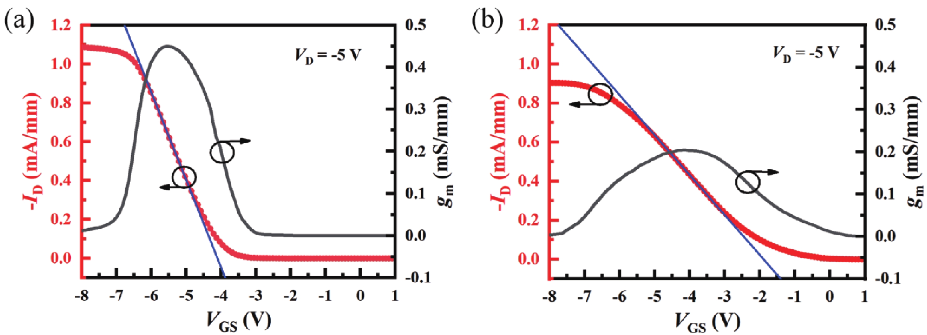
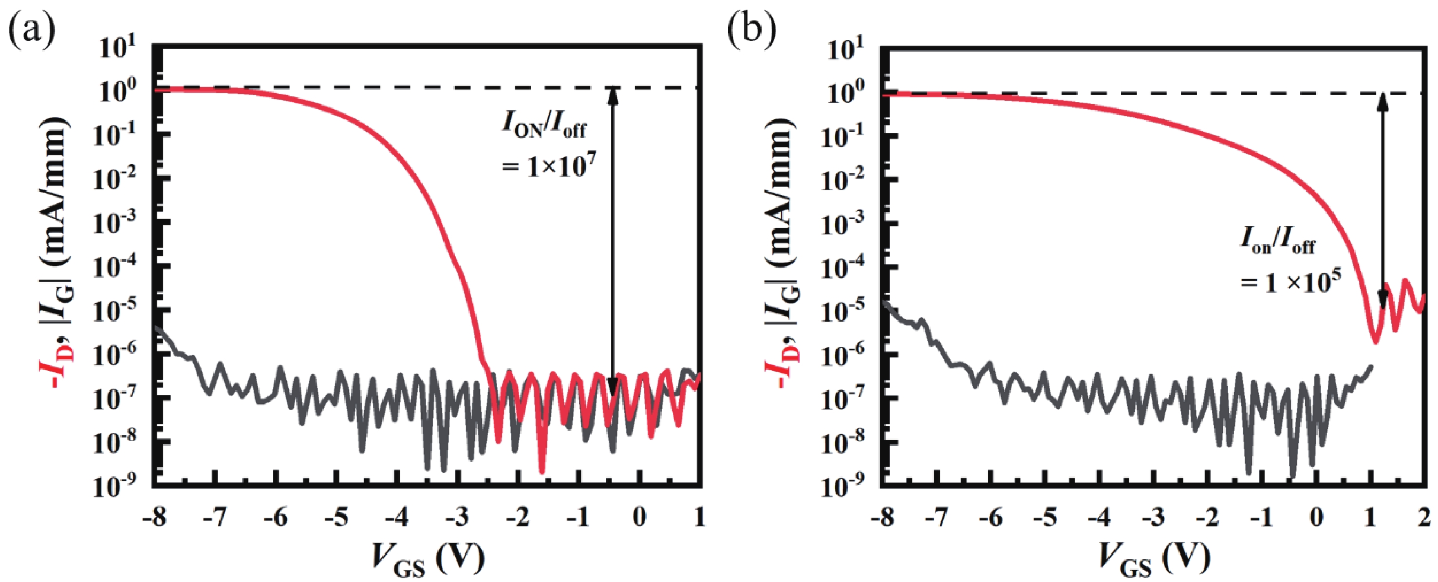
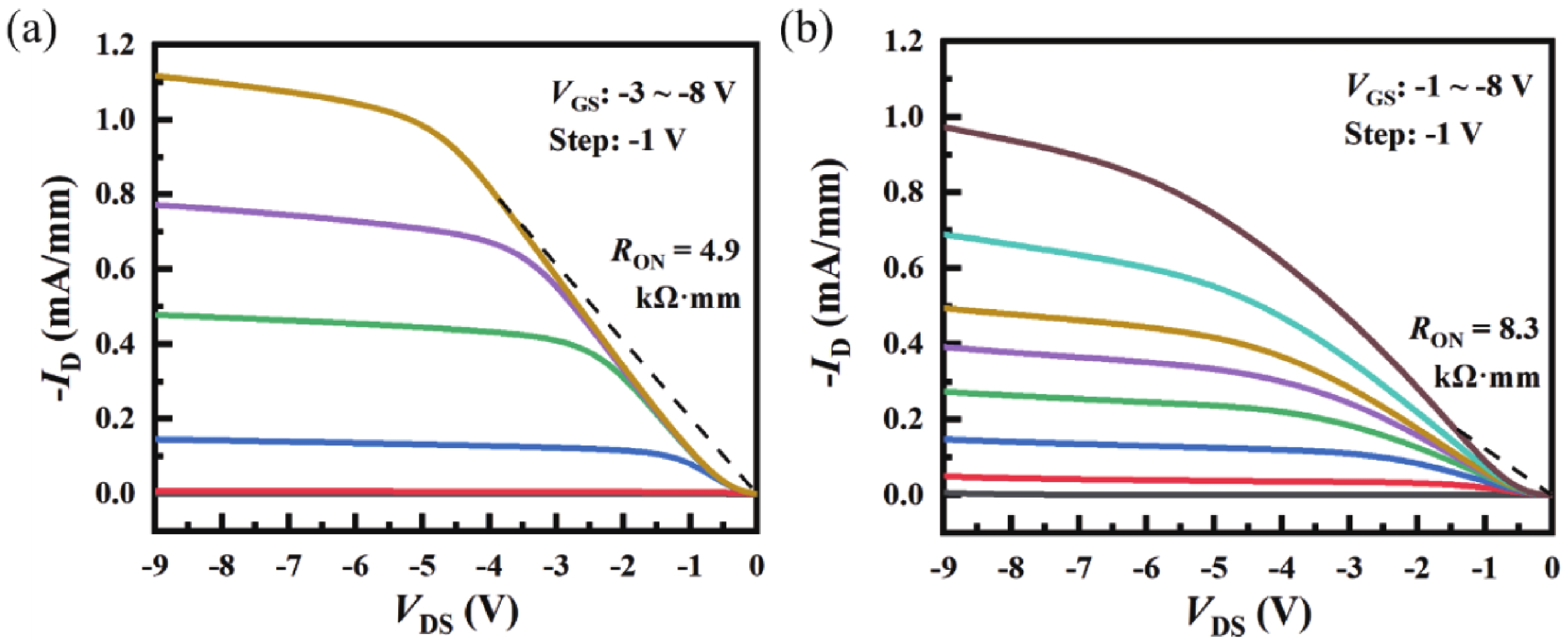
Table 1. Threshold voltages of device A and B extracted by different methods.
| Extract method | Linear extrapolation method at maximum transconductance |
Specific current method (−ID = 10 μA/mm) |
| VTH of device A (V) | −3.8 | −3.41 |
| VTH of device B (V) | −1.4 | −0.35 |
 DownLoad: CSV
Table 2. Benchmark of p-channel GaN-based FETs
| Work unit | Platform | VTHa (V) | ION-max (mA/mm) | ION/IOFFb |
| RWTH[2] | p-/i-GaN/AlInGaN/GaN/AlN | −1.12 (VD = −8 V) | 6.79 (VD = −8 V) | 7 |
| RWTH[25] | p-/i-GaN/AlInGaN/GaN/AlN | −0.5 (VD = −5 V) | 1.81 (VD = −5 V) | 8 |
| HRL[26] | p-/i-GaN/AlGaN/GaN | −0.36 (VD = −0.1 V) | 1.65 (VD = −5 V) | 6 |
| AIST[27] | p-/i-GaN/AlGaN/GaN | −0.75 (VD = −5 V) | 0.09 (VD = −5 V) | 3 |
| HKUST[28] | p-GaN/AlGaN/GaN | −1.7 (VD = −5 V) | 3.38 (VD = −5 V) | 7 |
| This work | p-GaN/AlGaN/GaN | −3.41 (VD = −5 V) | 1.12 (VD = −5 V) | 7 |
| aExtracted at −ID = 10 μA/mm. bExtracted at VD which is the same as noted in VTH and with overdriven VGS. |
||||
DownLoad: CSV
| [1] |
Zimmermann T, Neuburger M, Kunze M, et al. P-channel InGaN-HFET structure based on polarization doping. IEEE Electron Device Lett, 2004, 25, 450 doi: 10.1109/LED.2004.830285
|
| [2] |
Hahn H, Reuters B, Pooth A, et al. P-channel enhancement and depletion mode GaN-based HFETs with quaternary backbarriers. IEEE Trans Electron Devices, 2013, 60, 3005 doi: 10.1109/TED.2013.2272330
|
| [3] |
Chowdhury N, Lemettinen J, Xie Q Y, et al. P-channel GaN transistor based on p-GaN/AlGaN/GaN on Si. IEEE Electron Device Lett, 2019, 40, 1036 doi: 10.1109/LED.2019.2916253
|
| [4] |
Bader S J, Chaudhuri R, Nomoto K, et al. Gate-recessed E-mode p-channel HFET with high on-current based on GaN/AlN 2D hole gas. IEEE Electron Device Lett, 2018, 39, 1848 doi: 10.1109/LED.2018.2874190
|
| [5] |
Cao X A, Pearton S J, Zhang A P, et al. Electrical effects of plasma damage in p-GaN. Appl Phys Lett, 1999, 75, 2569 doi: 10.1063/1.125080
|
| [6] |
Cao X A, Pearton S J, Dang G T, et al. GaN n- and p-type Schottky diodes: Effect of dry etch damage. IEEE Trans Electron Devices, 2000, 47, 1320 doi: 10.1109/16.848271
|
| [7] |
Narita T, Kikuta D, Takahashi N, et al. Study of etching-induced damage in GaN by hard X-ray photoelectron spectroscopy. Phys Status Solidi A, 2011, 208, 1541 doi: 10.1002/pssa.201000952
|
| [8] |
Fu K, Fu H Q, Huang X Q, et al. Demonstration of 1.27 kV etch-then-regrow GaN p-n junctions with low leakage for GaN power electronics. IEEE Electron Device Lett, 2019, 40, 1728 doi: 10.1109/LED.2019.2941830
|
| [9] |
Hao R H, Fu K, Yu G H, et al. Normally-off p-GaN/AlGaN/GaN high electron mobility transistors using hydrogen plasma treatment. Appl Phys Lett, 2016, 109, 152106 doi: 10.1063/1.4964518
|
| [10] |
Nakamura S, Iwasa N, Senoh M, et al. Hole compensation mechanism of P-type GaN films. Jpn J Appl Phys, 1992, 31, 1258 doi: 10.1143/JJAP.31.1258
|
| [11] |
Hao R H, Li W Y, Fu K, et al. Breakdown enhancement and current collapse suppression by high-resistivity GaN cap layer in normally-off AlGaN/GaN HEMTs. IEEE Electron Device Lett, 2017, 38, 1567 doi: 10.1109/LED.2017.2749678
|
| [12] |
Wei X, Zhang X D, Sun C, et al. Improvement of breakdown voltage and ON-resistance in normally-OFF AlGaN/GaN HEMTs using etching-free p-GaN stripe array gate. IEEE Trans Electron Devices, 2021, 68, 5041 doi: 10.1109/TED.2021.3105088
|
| [13] |
Wei X, Zhang X D, Tang W X, et al. 2.0 kV/2.1 mΩ·cm2 lateral p-GaN/AlGaN/GaN hybrid anode diodes with hydrogen plasma treatment. IEEE Electron Device Lett, 2022, 43, 693 doi: 10.1109/LED.2022.3159240
|
| [14] |
Wei X, Zhang X D, Zhou X, et al. Dual Current and voltage sensitivity temperature sensor based on lateral p-GaN/AlGaN/GaN hybrid anode diode. IEEE Sens J, 2021, 21, 22459 doi: 10.1109/JSEN.2021.3109915
|
| [15] |
Fu H Q, Fu K, Alugubelli S R, et al. High voltage vertical GaN p-n diodes with hydrogen-plasma based guard rings. IEEE Electron Device Lett, 2020, 41, 127 doi: 10.1109/LED.2019.2954123
|
| [16] |
Takagi S, Toriumi A, Iwase M, et al. On the universality of inversion layer mobility in Si MOSFET's: Part I-effects of substrate impurity concentration. IEEE Trans Electron Devices, 1994, 41, 2357 doi: 10.1109/16.337449
|
| [17] |
Sah C T, Ning T H, Tschopp L L. The scattering of electrons by surface oxide charges and by lattice vibrations at the silicon-silicon dioxide interface. Surf Sci, 1972, 32, 561 doi: 10.1016/0039-6028(72)90183-5
|
| [18] |
Pérez-Tomás A, Brosselard P, Godignon P, et al. Field-effect mobility temperature modeling of 4H-SiC metal-oxide-semiconductor transistors. J Appl Phys, 2006, 100, 114508. doi: 10.1063/1.2395597
|
| [19] |
Lombardi C, Manzini S, Saporito A, et al. A physically based mobility model for numerical simulation of nonplanar devices. IEEE Trans Comput Aided Des Integr Circuits Syst, 1988, 7, 1164 doi: 10.1109/43.9186
|
| [20] |
Tang W X, Zhou J A, Yu G H, et al. Effects of the stepped sidewall morphology on the ON-state performance for vertical GaN trench-gate MOSFETs. Appl Phys Express, 2022, 15, 076502 doi: 10.35848/1882-0786/ac727d
|
| [21] |
Yang C, Fu H Q, Su P Y, et al. Demonstration of GaN-based metal–insulator–semiconductor junction by hydrogen plasma treatment. Appl Phys Lett, 2020, 117, 052105 doi: 10.1063/5.0018473
|
| [22] |
Calzolaro A, Mikolajick T, Wachowiak A. Status of aluminum oxide gate dielectric technology for insulated-gate GaN-based devices. Materials, 2022, 15, 791 doi: 10.3390/ma15030791
|
| [23] |
Wang Y, Wang M, Xie B, et al. High-performance normally-off Al2O3/GaN MOSFET using a wet etching-based gate recess technique. IEEE Electron Device Letters, 2013, 34(11), 1370 doi: 10.1109/LED.2013.2279844
|
| [24] |
He J L, Zhong Y Z, Zhou Y, et al. Recovery of p-GaN surface damage induced by dry etching for the formation of p-type Ohmic contact. Applied Physics Express, 2019, 12(5), 055507 doi: 10.7567/1882-0786/ab13d7
|
| [25] |
Reuters B, Hahn H, Pooth A, et al. Fabrication of p-channel heterostructure field effect transistors with polarization-induced two-dimensional hole gases at metal–polar GaN/AlInGaN interfaces. Journal of Physics D: Applied Physics, 2014, 47(17), 175103 doi: 10.1088/0022-3727/47/17/175103
|
| [26] |
Chu R, Cao Y, Chen M, et al. An experimental demonstration of GaN CMOS technology. IEEE Electron Device Letters, 2016, 37(3), 269 doi: 10.1109/LED.2016.2515103
|
| [27] |
Nakajima A, Kubota S, Tsutsui K, et al. GaN-based complementary metal–oxide–semiconductor inverter with normally off Pch and Nch MOSFETs fabricated using polarisation-induced holes and electron channels. IET Power Electronics, 2018, 11(4), 689 doi: 10.1049/iet-pel.2017.0376
|
| [28] |
Zheng Z, Song W, Zhang L, et al. High ION and ION/IOFF ratio enhancement-mode buried p-channel GaN MOSFETs on p-GaN gate power HEMT platform. IEEE Electron Device Letters, 2019, 41(1), 26 doi: 10.1109/LED.2019.2954035
|


Article views: 2207 Times PDF downloads: 156 Times Cited by: 0 Times
Received: 17 April 2023 Revised: 29 May 2023 Online: Accepted Manuscript: 27 August 2023Uncorrected proof: 09 October 2023Corrected proof: 11 October 2023Published: 10 November 2023
| Citation: |
Xiaotian Gao, Guohao Yu, Jiaan Zhou, Zheming Wang, Yu Li, Jijun Zhang, Xiaoyan Liang, Zhongming Zeng, Baoshun Zhang. Study of enhancement-mode GaN pFET with H plasma treated gate recess[J]. Journal of Semiconductors, 2023, 44(11): 112801. doi: 10.1088/1674-4926/44/11/112801
****
X T Gao, G H Yu, J A Zhou, Z M Wang, Y Li, J J Zhang, X Y Liang, Z M Zeng, B S Zhang. Study of enhancement-mode GaN pFET with H plasma treated gate recess[J]. J. Semicond, 2023, 44(11): 112801. doi: 10.1088/1674-4926/44/11/112801

|
 Xiaotian Gao:received his BS degree from Nanjing University of Science and Technology in 2019. He is now an MS student at Shanghai University. His research focuses on the optimization of performance for GaN pFET devices
 Baoshun Zhang:received his BS degree from Changchun University of Science and Technology in 1994 and PhD degree from the Institute of Semiconductors, Chinese Academy of Sciences in 2003. Then he joined in Hong Kong University of Science and Technology. Currently, he is a researcher at Suzhou Institute of Nano-Tech and Nano-Bionics, Chinese Academy of Sciences, and his research interests include semiconductor material growth and device technology research
| [1] |
Zimmermann T, Neuburger M, Kunze M, et al. P-channel InGaN-HFET structure based on polarization doping. IEEE Electron Device Lett, 2004, 25, 450 doi: 10.1109/LED.2004.830285
|
| [2] |
Hahn H, Reuters B, Pooth A, et al. P-channel enhancement and depletion mode GaN-based HFETs with quaternary backbarriers. IEEE Trans Electron Devices, 2013, 60, 3005 doi: 10.1109/TED.2013.2272330
|
| [3] |
Chowdhury N, Lemettinen J, Xie Q Y, et al. P-channel GaN transistor based on p-GaN/AlGaN/GaN on Si. IEEE Electron Device Lett, 2019, 40, 1036 doi: 10.1109/LED.2019.2916253
|
| [4] |
Bader S J, Chaudhuri R, Nomoto K, et al. Gate-recessed E-mode p-channel HFET with high on-current based on GaN/AlN 2D hole gas. IEEE Electron Device Lett, 2018, 39, 1848 doi: 10.1109/LED.2018.2874190
|
| [5] |
Cao X A, Pearton S J, Zhang A P, et al. Electrical effects of plasma damage in p-GaN. Appl Phys Lett, 1999, 75, 2569 doi: 10.1063/1.125080
|
| [6] |
Cao X A, Pearton S J, Dang G T, et al. GaN n- and p-type Schottky diodes: Effect of dry etch damage. IEEE Trans Electron Devices, 2000, 47, 1320 doi: 10.1109/16.848271
|
| [7] |
Narita T, Kikuta D, Takahashi N, et al. Study of etching-induced damage in GaN by hard X-ray photoelectron spectroscopy. Phys Status Solidi A, 2011, 208, 1541 doi: 10.1002/pssa.201000952
|
| [8] |
Fu K, Fu H Q, Huang X Q, et al. Demonstration of 1.27 kV etch-then-regrow GaN p-n junctions with low leakage for GaN power electronics. IEEE Electron Device Lett, 2019, 40, 1728 doi: 10.1109/LED.2019.2941830
|
| [9] |
Hao R H, Fu K, Yu G H, et al. Normally-off p-GaN/AlGaN/GaN high electron mobility transistors using hydrogen plasma treatment. Appl Phys Lett, 2016, 109, 152106 doi: 10.1063/1.4964518
|
| [10] |
Nakamura S, Iwasa N, Senoh M, et al. Hole compensation mechanism of P-type GaN films. Jpn J Appl Phys, 1992, 31, 1258 doi: 10.1143/JJAP.31.1258
|
| [11] |
Hao R H, Li W Y, Fu K, et al. Breakdown enhancement and current collapse suppression by high-resistivity GaN cap layer in normally-off AlGaN/GaN HEMTs. IEEE Electron Device Lett, 2017, 38, 1567 doi: 10.1109/LED.2017.2749678
|
| [12] |
Wei X, Zhang X D, Sun C, et al. Improvement of breakdown voltage and ON-resistance in normally-OFF AlGaN/GaN HEMTs using etching-free p-GaN stripe array gate. IEEE Trans Electron Devices, 2021, 68, 5041 doi: 10.1109/TED.2021.3105088
|
| [13] |
Wei X, Zhang X D, Tang W X, et al. 2.0 kV/2.1 mΩ·cm2 lateral p-GaN/AlGaN/GaN hybrid anode diodes with hydrogen plasma treatment. IEEE Electron Device Lett, 2022, 43, 693 doi: 10.1109/LED.2022.3159240
|
| [14] |
Wei X, Zhang X D, Zhou X, et al. Dual Current and voltage sensitivity temperature sensor based on lateral p-GaN/AlGaN/GaN hybrid anode diode. IEEE Sens J, 2021, 21, 22459 doi: 10.1109/JSEN.2021.3109915
|
| [15] |
Fu H Q, Fu K, Alugubelli S R, et al. High voltage vertical GaN p-n diodes with hydrogen-plasma based guard rings. IEEE Electron Device Lett, 2020, 41, 127 doi: 10.1109/LED.2019.2954123
|
| [16] |
Takagi S, Toriumi A, Iwase M, et al. On the universality of inversion layer mobility in Si MOSFET's: Part I-effects of substrate impurity concentration. IEEE Trans Electron Devices, 1994, 41, 2357 doi: 10.1109/16.337449
|
| [17] |
Sah C T, Ning T H, Tschopp L L. The scattering of electrons by surface oxide charges and by lattice vibrations at the silicon-silicon dioxide interface. Surf Sci, 1972, 32, 561 doi: 10.1016/0039-6028(72)90183-5
|
| [18] |
Pérez-Tomás A, Brosselard P, Godignon P, et al. Field-effect mobility temperature modeling of 4H-SiC metal-oxide-semiconductor transistors. J Appl Phys, 2006, 100, 114508. doi: 10.1063/1.2395597
|
| [19] |
Lombardi C, Manzini S, Saporito A, et al. A physically based mobility model for numerical simulation of nonplanar devices. IEEE Trans Comput Aided Des Integr Circuits Syst, 1988, 7, 1164 doi: 10.1109/43.9186
|
| [20] |
Tang W X, Zhou J A, Yu G H, et al. Effects of the stepped sidewall morphology on the ON-state performance for vertical GaN trench-gate MOSFETs. Appl Phys Express, 2022, 15, 076502 doi: 10.35848/1882-0786/ac727d
|
| [21] |
Yang C, Fu H Q, Su P Y, et al. Demonstration of GaN-based metal–insulator–semiconductor junction by hydrogen plasma treatment. Appl Phys Lett, 2020, 117, 052105 doi: 10.1063/5.0018473
|
| [22] |
Calzolaro A, Mikolajick T, Wachowiak A. Status of aluminum oxide gate dielectric technology for insulated-gate GaN-based devices. Materials, 2022, 15, 791 doi: 10.3390/ma15030791
|
| [23] |
Wang Y, Wang M, Xie B, et al. High-performance normally-off Al2O3/GaN MOSFET using a wet etching-based gate recess technique. IEEE Electron Device Letters, 2013, 34(11), 1370 doi: 10.1109/LED.2013.2279844
|
| [24] |
He J L, Zhong Y Z, Zhou Y, et al. Recovery of p-GaN surface damage induced by dry etching for the formation of p-type Ohmic contact. Applied Physics Express, 2019, 12(5), 055507 doi: 10.7567/1882-0786/ab13d7
|
| [25] |
Reuters B, Hahn H, Pooth A, et al. Fabrication of p-channel heterostructure field effect transistors with polarization-induced two-dimensional hole gases at metal–polar GaN/AlInGaN interfaces. Journal of Physics D: Applied Physics, 2014, 47(17), 175103 doi: 10.1088/0022-3727/47/17/175103
|
| [26] |
Chu R, Cao Y, Chen M, et al. An experimental demonstration of GaN CMOS technology. IEEE Electron Device Letters, 2016, 37(3), 269 doi: 10.1109/LED.2016.2515103
|
| [27] |
Nakajima A, Kubota S, Tsutsui K, et al. GaN-based complementary metal–oxide–semiconductor inverter with normally off Pch and Nch MOSFETs fabricated using polarisation-induced holes and electron channels. IET Power Electronics, 2018, 11(4), 689 doi: 10.1049/iet-pel.2017.0376
|
| [28] |
Zheng Z, Song W, Zhang L, et al. High ION and ION/IOFF ratio enhancement-mode buried p-channel GaN MOSFETs on p-GaN gate power HEMT platform. IEEE Electron Device Letters, 2019, 41(1), 26 doi: 10.1109/LED.2019.2954035
|

 WeChat ID
Journal of Semiconductors © 2017 All Rights Reserved 京ICP备05085259号-2


