J. Semicond. > 2023, Volume 44 > Issue 12 > 122101

ARTICLES

Switchable hidden spin polarization and negative Poisson's ratio in two-dimensional antiferroelectric wurtzite crystals

Zhuang Ma1, §, Jingwen Jiang1, §, Gui Wang1, Peng Zhang1, Yiling Sun1, Zhengfang Qian1, Jiaxin Zheng2, Wen Xiong3, Fei Wang4, Xiuwen Zhang1, 5 and Pu Huang1,

+ Author Affiliations

 Corresponding author: Pu Huang, arvin_huang@szu.edu.cn

DOI: 10.1088/1674-4926/44/12/122101

PDF

Turn off MathJax

Abstract: Two-dimensional (2D) antiferroelectric materials have raised great research interest over the last decade. Here, we reveal a type of 2D antiferroelectric (AFE) crystal where the AFE polarization direction can be switched by a certain degree in the 2D plane. Such 2D functional materials are realized by stacking the exfoliated wurtzite (wz) monolayers with “self-healable” nature, which host strongly coupled ferroelasticity/antiferroelectricity and benign stability. The AFE candidates, i.e., ZnX and CdX (X = S, Se, Te), are all semiconductors with direct bandgap at Γ point, which harbors switchable antiferroelectricity and ferroelasticity with low transition barriers, hidden spin polarization, as well as giant in-plane negative Poisson's ratio (NPR), enabling the co-tunability of hidden spin characteristics and auxetic magnitudes via AFE switching. The 2D AFE wz crystals provide a platform to probe the interplay of 2D antiferroelectricity, ferroelasticity, NPR, and spin effects, shedding new light on the rich physics and device design in wz semiconductors.

Key words: wurtzite crystalmultiferroicshidden spin polarizationnegative Poisson's ratio


[1]
Kittel C. Theory of antiferroelectric crystals. Phys Rev, 1951, 82, 729 doi: 10.1103/PhysRev.82.729
[2]
Shirane G, Sawaguchi E, Takagi Y. Dielectric properties of lead zirconate. Phys Rev, 1951, 84, 476 doi: 10.1103/PhysRev.84.476
[3]
Shirane G. Ferroelectricity and antiferroelectricity in ceramic PbZrO3 containing Ba or Sr. Phys Rev, 1952, 86, 219 doi: 10.1103/PhysRev.86.219
[4]
Sawaguchi E, Maniwa H, Hoshino S. Antiferroelectric structure of lead zirconate. Phys Rev, 1951, 83, 1078 doi: 10.1103/PhysRev.83.1078
[5]
Randall C A, Fan Z M, Reaney I, et al. Antiferroelectrics: History, fundamentals, crystal chemistry, crystal structures, size effects, and applications. J Am Ceram Soc, 2021, 104, 3775 doi: 10.1111/jace.17834
[6]
Liu Z, Lu T, Ye J M, et al. Antiferroelectrics for energy storage applications: A review. Adv Mater Technol, 2018, 3, 1800111 doi: 10.1002/admt.201800111
[7]
Qi H, Zuo R Z, Xie A W, et al. Ultrahigh energy-storage density in NaNbO3-based lead-free relaxor antiferroelectric ceramics with nanoscale domains. Adv Funct Mater, 2019, 29, 1903877 doi: 10.1002/adfm.201903877
[8]
Zhou Z Y, Yang Q, Liu M, et al. Antiferroelectric materials, applications and recent progress on multiferroic heterostructures. SPIN, 2015, 5, 1530001 doi: 10.1142/S2010324715300017
[9]
Narayanan M, Ma B H, Tong S, et al. Electrical properties of Pb0.92La0.08Zr0.52Ti0.48O3 thin films grown on SrRuO3 buffered nickel and silicon substrates by chemical solution deposition. Int J Appl Ceram Technol, 2012, 9, 45 doi: 10.1111/j.1744-7402.2011.02693.x
[10]
Huang B Y, Lu Z X, Zhang Y, et al. Antiferroelectric polarization switching and dynamic scaling of energy storage: A Monte Carlo simulation. J Appl Phys, 2016, 119, 174103 doi: 10.1063/1.4948476
[11]
Payne A, Brewer O, Leff A, et al. Dielectric, energy storage, and loss study of antiferroelectric-like Al-doped HfO2 thin films. Appl Phys Lett, 2020, 117, 221104 doi: 10.1063/5.0029706
[12]
Bharadwaja S S N, Krupanidhi S B. Backward switching phenomenon from field forced ferroelectric to antiferroelectric phases in antiferroelectric PbZrO3 thin films. J Appl Phys, 2001, 89, 4541 doi: 10.1063/1.1331659
[13]
Guan Z, Zhao Y F, Wang X T, et al. Electric-field-induced room-temperature antiferroelectric–ferroelectric phase transition in van der waals layered GeSe. ACS Nano, 2022, 16, 1308 doi: 10.1021/acsnano.1c09183
[14]
Liu C S, Chen H W, Wang S Y, et al. Two-dimensional materials for next-generation computing technologies. Nat Nanotechnol, 2020, 15, 545 doi: 10.1038/s41565-020-0724-3
[15]
Ding W J, Zhu J B, Wang Z, et al. Prediction of intrinsic two-dimensional ferroelectrics in In2Se3 and other III2-VI3 van der Waals materials. Nat Commun, 2017, 8, 14956 doi: 10.1038/ncomms14956
[16]
Liu F C, You L, Seyler K L, et al. Room-temperature ferroelectricity in CuInP2S6 ultrathin flakes. Nat Commun, 2016, 7, 12357 doi: 10.1038/ncomms12357
[17]
Wu M H, Zeng X C. Intrinsic ferroelasticity and/or multiferroicity in two-dimensional phosphorene and phosphorene analogues. Nano Lett, 2016, 16, 3236 doi: 10.1021/acs.nanolett.6b00726
[18]
Dziaugys A, Kelley K, Brehm J A, et al. Piezoelectric domain walls in van der Waals antiferroelectric CuInP2Se6. Nat Commun, 2020, 11, 1 doi: 10.1038/s41467-020-17137-0
[19]
Ding J, Shao D F, Li M, et al. Two-dimensional antiferroelectric tunnel junction. Phys Rev Lett, 2021, 126, 057601 doi: 10.1103/PhysRevLett.126.057601
[20]
Xu C, Chen Y C, Cai X B, et al. Two-dimensional antiferroelectricity in nanostripe-ordered In2Se3. Phys Rev Lett, 2020, 125, 047601 doi: 10.1103/PhysRevLett.125.047601
[21]
Guan S, Luo J W. Electrically switchable hidden spin polarization in antiferroelectric crystals. Phys Rev B, 2020, 102, 184104 doi: 10.1103/PhysRevB.102.184104
[22]
Chen S B, Sun H S, Ding J F, et al. Unconventional distortion induced two-dimensional multiferroicity in a CrO3 monolayer. Nanoscale, 2021, 13, 13048 doi: 10.1039/D1NR02335G
[23]
Zhao J L, Wang X Y, Chen H H, et al. Two-dimensional ferroelectric Ga2O3 bilayers with unusual strain-engineered interlayer interactions. Chem Mater, 2022, 34, 3648 doi: 10.1021/acs.chemmater.1c04245
[24]
Wu Z Y, Liu X T, Ji C M, et al. Discovery of an above-room-temperature antiferroelectric in two-dimensional hybrid perovskite. J Am Chem Soc, 2019, 141, 3812 doi: 10.1021/jacs.8b13827
[25]
Han S G, Liu X T, Liu Y, et al. High-temperature antiferroelectric of lead iodide hybrid perovskites. J Am Chem Soc, 2019, 141, 12470 doi: 10.1021/jacs.9b05124
[26]
Li M F, Han S G, Liu Y, et al. Soft perovskite-type antiferroelectric with giant electrocaloric strength near room temperature. J Am Chem Soc, 2020, 142, 20744 doi: 10.1021/jacs.0c09601
[27]
Wool R P. Self-healing materials: A review. Soft Matter, 2008, 4, 400 doi: 10.1039/b711716g
[28]
Na S R, Kim Y, Lee C G, et al. Adhesion and self-healing between monolayer molybdenum disulfide and silicon oxide. Sci Rep, 2017, 7, 14740 doi: 10.1038/s41598-017-14921-9
[29]
Zhang X K, Liao Q L, Kang Z, et al. Self-healing originated van der Waals homojunctions with strong interlayer coupling for high-performance photodiodes. ACS Nano, 2019, 13, 3280 doi: 10.1021/acsnano.8b09130
[30]
Ma Z, Huang P, Li J, et al. Multiferroicity and giant in-plane negative Poisson’s ratio in wurtzite monolayers. Npj Comput Mater, 2022, 8, 1 doi: 10.1038/s41524-022-00740-8
[31]
Kenji Y, Wang X R, Kenji W, et al. Stacking-engineered ferroelectricity in bilayer boron nitride. Science, 2021, 372(6549), 1458 doi: 10.1126/science.abd3230
[32]
Vizner Stern M, Waschitz Y, Cao W, et al. Interfacial ferroelectricity by van der Waals sliding. Science, 2021, 372(6549), 1462 doi: 10.1126/science.abe8177
[33]
Lee C G, Wei X D, Kysar J W, et al. Measurement of the elastic properties and intrinsic strength of monolayer graphene. Science, 2008, 321, 385 doi: 10.1126/science.1157996
[34]
Wu M H, Li J. Sliding ferroelectricity in 2D van der Waals materials: Related physics and future opportunities. Proc Natl Acad Sci U S A, 2021, 118, e2115703118 doi: 10.1073/pnas.2115703118
[35]
Wu M H. Two-dimensional van der Waals ferroelectrics: Scientific and technological opportunities. ACS Nano, 2021, 15, 9229 doi: 10.1021/acsnano.0c08483
[36]
Li L, Wu M H. Binary compound bilayer and multilayer with vertical polarizations: Two-dimensional ferroelectrics, multiferroics, and nanogenerators. ACS Nano, 2017, 11, 6382 doi: 10.1021/acsnano.7b02756
[37]
Calderon S V, Hayden J, Baksa S M, et al. Atomic-scale polarization switching in wurtzite ferroelectrics. Science, 2023, 380, 1034 doi: 10.1126/science.adh7670
[38]
Dronskowski R, Bloechl P E. Crystal orbital Hamilton populations (COHP): Energy-resolved visualization of chemical bonding in solids based on density-functional calculations. J Phys Chem, 1993, 97, 8617 doi: 10.1021/j100135a014
[39]
Xu C, Mao J F, Guo X Y, et al. Two-dimensional ferroelasticity in van der Waals β’-In2Se3. Nat Commun, 2021, 12, 3665 doi: 10.1038/s41467-021-23882-7
[40]
Zhou J, Xu H W, Li Y F, et al. Opto-mechanics driven fast martensitic transition in two-dimensional materials. Nano Lett, 2018, 18, 7794 doi: 10.1021/acs.nanolett.8b03559
[41]
Pan Y M, Zhou J. Toggling valley-spin locking and nonlinear optical properties of single-element multiferroic monolayers via light. Phys Rev Applied, 2020, 14, 014024 doi: 10.1103/PhysRevApplied.14.014024
[42]
Xu B, Li S C, Jiang K, et al. Switching of the magnetic anisotropy via strain in two dimensional multiferroic materials: CrSX (X = Cl, Br, I). Appl Phys Lett, 2020, 116, 052403 doi: 10.1063/1.5140644
[43]
Ma Y D, Kou L Z, Huang B B, et al. Two-dimensional ferroelastic topological insulators in single-layer Janus transition metal dichalcogenides MSSe (M = Mo, W). Phys Rev B, 2018, 98, 085420 doi: 10.1103/PhysRevB.98.085420
[44]
Zhang T, Liang Y, Xu X L, et al. Ferroelastic-ferroelectric multiferroics in a bilayer lattice. Phys Rev B, 2021, 103, 165420 doi: 10.1103/PhysRevB.103.165420
[45]
Li W B, Li J. Ferroelasticity and domain physics in two-dimensional transition metal dichalcogenide monolayers. Nat Commun, 2016, 7, 10843 doi: 10.1038/ncomms10843
[46]
Kim K S, Zhao Y, Jang H, et al. Large-scale pattern growth of graphene films for stretchable transparent electrodes. Nature, 2009, 457, 706 doi: 10.1038/nature07719
[47]
Bertolazzi S, Brivio J, Kis A. Stretching and breaking of ultrathin MoS2. ACS Nano, 2011, 5, 9703 doi: 10.1021/nn203879f
[48]
Tao J, Shen W F, Wu S, et al. Mechanical and electrical anisotropy of few-layer black phosphorus. ACS Nano, 2015, 9, 11362 doi: 10.1021/acsnano.5b05151
[49]
Zhang X W, Liu Q H, Luo J W, et al. Hidden spin polarization in inversion-symmetric bulk crystals. Nat Phys, 2014, 10, 387 doi: 10.1038/nphys2933
[50]
Beaulieu S, Schusser J, Dong S, et al. Revealing hidden orbital pseudospin texture with time-reversal dichroism in photoelectron angular distributions. Phys Rev Lett, 2020, 125, 216404 doi: 10.1103/PhysRevLett.125.216404
[51]
Tu J, Chen X B, Ruan X Z, et al. Direct observation of hidden spin polarization in 2H–MoTe2. Phys Rev B, 2020, 101, 035102 doi: 10.1103/PhysRevB.101.035102
[52]
Zhang K, Zhao S X, Hao Z Y, et al. Observation of spin-momentum-layer locking in a centrosymmetric crystal. Phys Rev Lett, 2021, 127, 126402 doi: 10.1103/PhysRevLett.127.126402
[53]
Yao W, Wang E Y, Huang H Q, et al. Direct observation of spin-layer locking by local Rashba effect in monolayer semiconducting PtSe2 film. Nat Commun, 2017, 8, 14216 doi: 10.1038/ncomms14216
[54]
Cheng C, Sun J T, Chen X R, et al. Hidden spin polarization in the 1T-phase layered transition-metal dichalcogenides MX2 (M = Zr, Hf; X = S, Se, Te). Sci Bull, 2018, 63, 85 doi: 10.1016/j.scib.2017.12.003
[55]
Yuan L D, Liu Q H, Zhang X W, et al. Uncovering and tailoring hidden Rashba spin–orbit splitting in centrosymmetric crystals. Nat Commun, 2019, 10, 1 doi: 10.1038/s41467-018-07882-8
[56]
Liu Q H, Zhang X W, Jin H, et al. Search and design of nonmagnetic centrosymmetric layered crystals with large local spin polarization. Phys Rev B, 2015, 91, 235204 doi: 10.1103/PhysRevB.91.235204
[57]
Liu Q H, Guo Y Z, Freeman A J. Tunable rashba effect in two-dimensional LaOBiS2 films: Ultrathin candidates for spin field effect transistors. Nano Lett, 2013, 13, 5264 doi: 10.1021/nl4027346
[58]
Zhang X T, Zhang F, Wang Y X, et al. Defect-controlled nucleation and orientation of WSe2 on hBN: A route to single-crystal epitaxial monolayers. ACS Nano, 2019, 13, 3341 doi: 10.1021/acsnano.8b09230
[59]
Brown P D, Russell G J, Woods J. Anisotropic defect distribution in ZnSe/ZnS epitaxial layers grown by metalorganic vapor-phase epitaxy on (001)-oriented GaAs. J Appl Phys, 1989, 66, 129 doi: 10.1063/1.343891
[60]
Han Y M, Li M Y, Jung G S, et al. Sub-nanometre channels embedded in two-dimensional materials. Nat Mater, 2018, 17, 129 doi: 10.1038/nmat5038
[61]
Jain S C, Willander M, Narayan J, et al. III–nitrides: Growth, characterization, and properties. J Appl Phys, 2000, 87, 965 doi: 10.1063/1.371971
[62]
Xiao C C, Wang F, Yang S A, et al. Elemental ferroelectricity and antiferroelectricity in group-V monolayer. Adv Funct Mater, 2018, 28, 1707383 doi: 10.1002/adfm.201707383
[63]
Liu C, Gao R L, Cheng X L, et al. First-principles study of ferroelectricity, antiferroelectricity, and ferroelasticity in two-dimensional γ-AlOOH. Phys Rev B, 2023, 107, L121402 doi: 10.1103/PhysRevB.107.L121402
[64]
Jiang K, Ji J P, Gong W B, et al. Mechanical cleavage of non-van der Waals structures towards two-dimensional crystals. Nat Synth, 2023, 2, 58 doi: 10.1038/s44160-022-00182-6
[65]
Puthirath Balan A, Radhakrishnan S, Woellner C F, et al. Exfoliation of a non-van der Waals material from iron ore hematite. Nat Nanotechnol, 2018, 13, 602 doi: 10.1038/s41565-018-0134-y
[66]
Wu H, Zhang W F, Yang L, et al. Strong intrinsic room-temperature ferromagnetism in freestanding non-van der Waals ultrathin 2D crystals. Nat Commun, 2021, 12, 5688 doi: 10.1038/s41467-021-26009-0
[67]
Staudinger P, Moselund K E, Schmid H. Exploring the size limitations of wurtzite III–V film growth. Nano Lett, 2020, 20, 686 doi: 10.1021/acs.nanolett.9b04507
[68]
Yue G H, Yan P X, Yan D, et al. Synthesis of two-dimensional micron-sized single-crystalline ZnS thin nanosheets and their photoluminescence properties. J Cryst Growth, 2006, 293, 428 doi: 10.1016/j.jcrysgro.2006.05.053
[69]
Wang L, Xiong K L, He Y K, et al. Epitaxial growth of wafer-scale two-dimensional polytypic ZnS thin films on ZnO substrates. Cryst Eng Comm, 2017, 19, 2294 doi: 10.1039/C7CE00428A
[70]
Wang Z W, Wen X D, Hoffmann R, et al. Reconstructing a solid-solid phase transformation pathway in CdSe nanosheets with associated soft ligands. Proc Natl Acad Sci USA, 2010, 107, 17119 doi: 10.1073/pnas.1011224107
[71]
Wang C S, Ke X X, Wang J J, et al. Ferroelastic switching in a layered-perovskite thin film. Nat Commun, 2016, 7, 1 doi: doi.org/10.1038/ncomms10636
[72]
Park M H, Kim H J, Kim Y J, et al. Toward a multifunctional monolithic device based on pyroelectricity and the electrocaloric effect of thin antiferroelectric Hf xZr1− xO2 films. Nano Energy, 2015, 12, 131 doi: 10.1016/j.nanoen.2014.09.025
[73]
Mischenko A S, Zhang Q, Scott J F, et al. Giant electrocaloric effect in thin-film PbZr0.95Ti0.05O3. Science, 2006, 311, 1270 doi: 10.1126/science.1123811
[74]
Geng W P, Liu Y, Meng X J, et al. Giant negative electrocaloric effect in antiferroelectric La-doped Pb(ZrTi)O3 thin films near room temperature. Adv Mater, 2015, 27, 3165 doi: 10.1002/adma.201501100
[75]
Hao X H, Zhai J W, Kong L B, et al. A comprehensive review on the progress of lead zirconate-based antiferroelectric materials. Prog Mater Sci, 2014, 63, 1 doi: 10.1016/j.pmatsci.2014.01.002
[76]
Bharadwaja S S N, Krupanidhi S B. Antiferroelectric thin films for MEMs applications. Ferroelectrics, 2001, 263, 39 doi: 10.1080/00150190108225176
[77]
Xu B M, Cross L E, Bernstein J J. Ferroelectric and antiferroelectric films for microelectromechanical systems applications. Thin Solid Films, 2000, 377/378, 712 doi: 10.1016/S0040-6090(00)01322-5
[78]
Guo M Y, Wu M, Gao W W, et al. Giant negative electrocaloric effect in antiferroelectric PbZrO3 thin films in an ultra-low temperature range. J Mater Chem C, 2019, 7, 617 doi: 10.1039/C8TC05108A
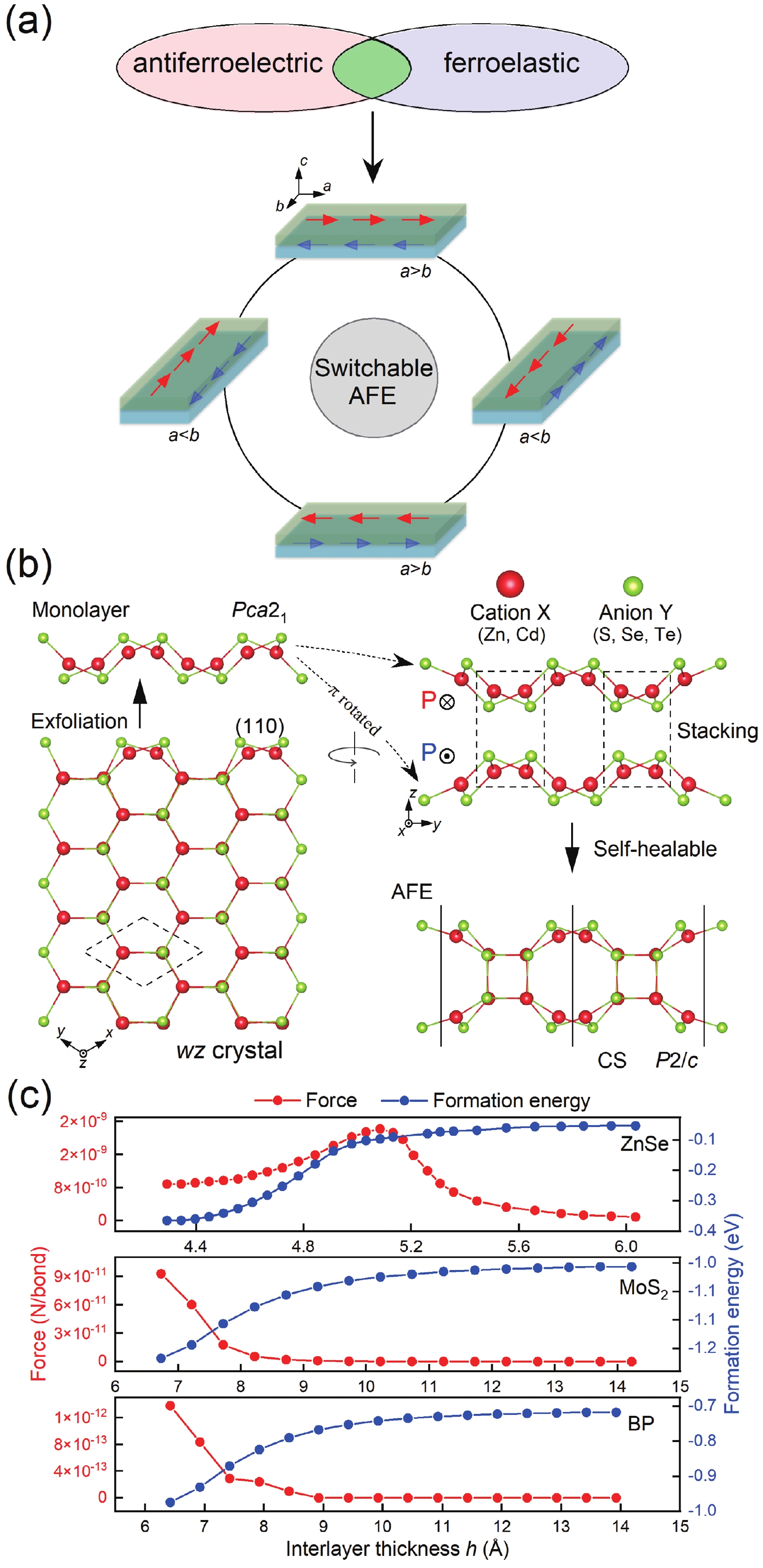
Fig. 1.  (Color online) (a) Schematic depiction of how the ferroelastic-antiferroelectric is induced from antiferroelectricity and ferroelasticity, in which the red and blue arrows indicate the FE polarization for each sector of the system. (b) Building the 2D AFE structures (cation X = Zn, Cd; anion Y = S, Se, Te, P2/c symmetry) with the wz monolayer (Pca21 symmetry) as building blocks. Here, the wz monolayer is exfoliated from the wz bulk thick layer with (110) crystallographic plane, which can bond spontaneously with another one when stacked vertically due to the inherent self-healable nature. (c) The average interlayer force (per bond in unit cell) and formation energy as a function of the slab thickness h in the 2D AFE ZnSe, 2L MoS2 and 2L black phosphorene, respectively.

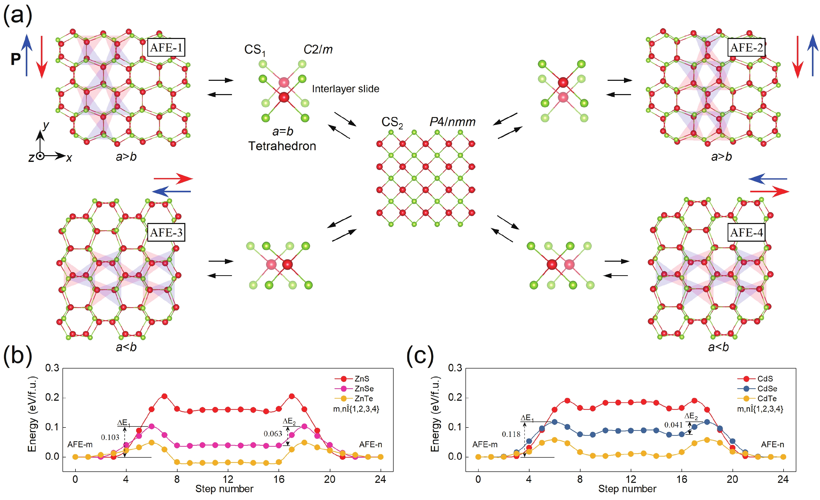
Fig. 2.  (Color online) (a) Feasible phase transition channels for the 2D AFE structure. The triangle in either AFE-1/2/3/4 structure can transform into tetrahedra with the phase transition into CS1 C2/m structure, which further changes into CS2 P4/nmm structure due to the interlayer slipping for tetrahedra (a/4 or b/4 along the lattice direction). The continuing movement of the tetrahedra would make the structure restore the AFE phase through the C2/m structure, forming the AFE phase changing channel with π (inversed) or π/2 rotated triangle configurations. Here, the blue and red arrows denote the polarization direction within each layer of the AFE-n structure, as accentuated by the congruent hues presenting in the corresponding triangles. (b), (c) Phase changing barrier for the 2D AFE structures, where the ∆E1 and ∆E2 depict the barrier heights for the AFE-m,n → CS1 and CS1 → CS2 phase changing process.

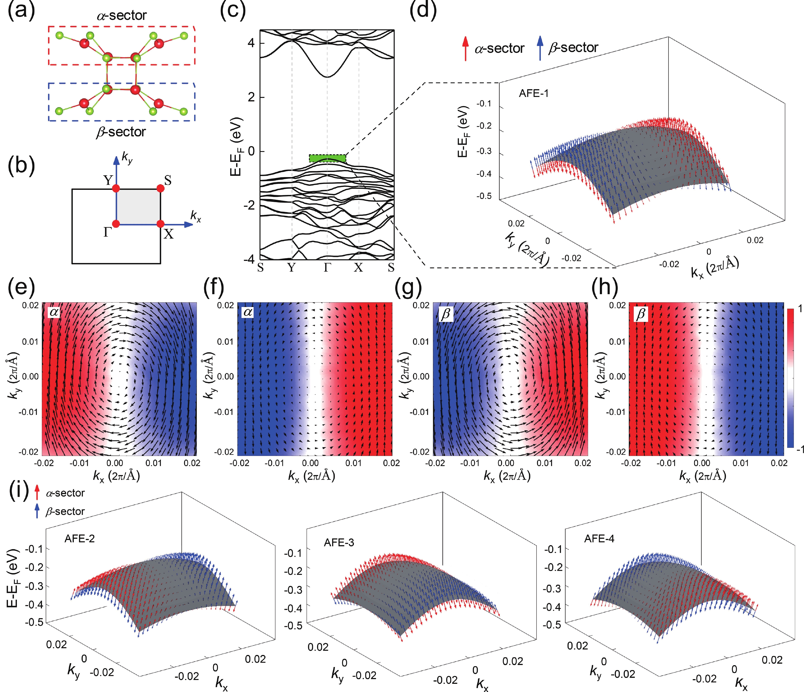
Fig. 3.  (Color online) (a) Crystal structure for 2D AFE ZnSe with boxed α-sector and β-sector for hidden spin projection. (b) The first Brillouin zone of the 2D AFE structure, where the high symmetry k points (Γ, X, Y, and S) are indicated. (c) Band structure (HSE06 + SOC) for 2D AFE ZnSe. (d) 3D spin texture near the VBM region highlighted in (c), in which the red and blue arrows indicate the spin polarization contributed by α- and β-sector and the magnitude of spin vectors depend on the strength of SOC and spin splitting. Corresponding 2D diagram of the spin polarizations of α-sector (e), (f) and β-sector (g), (h) and the color scheme indicates the out-of-plane spin component, the shade of color bar represents the magnitude of the hidden spin polarization. (i) Switchable spin texture projected to the k space for the 2D AFE ZnSe around VBM, which is expected by tuning the in-plane AFE polarization.

Fig. 4.  (Color online) (a) Top view for ZnSe AFE structure, in which we denote the projections of triangle and tetrahedra along b-axis by ∆d1 and ∆d2, respectively. (b) Variation of the ∆d1 and ∆d2 with strain along lattice a. (c) PDOS for the ZnX (X = S, Se, Te), indicating the localized/dispersive cation s/anion p state. (d) Anisotropic in-plane s-px/y and out-of-plane s-pz orbital interactions in ZnX. (e) In-plane NPR response for 2D AFE ZnSe, which can be flipped through the AFE transition. (f) Statistical NPR values for the 2D AFE structures, among which three members have NPR exceeding −0.450.

Table 1.   Lattice constants a and b (Å), FC reversible strains ε (%), band gaps (eV) with PBE and HSE06 functionals, transition barrier ΔE1 (eV/f.u.) for AFE-m,n → CS1 and ΔE2 (eV/f.u.) for CS1 → CS2 phase changing process, and NPR value v along lattice direction of wz AFE structures.

Crystal a (Å) b (Å) ε (%) HSESOC (eV) PBESOC (eV) ΔE1 (eV/f.u.) ΔE2 (eV/f.u.) va vb
ZnS 7.39 6.55 12.8 3.76 2.60 0.205 0.051 −0.398 −0.206
ZnSe 7.63 6.81 12.0 3.02 2.00 0.103 0.063 −0.469 −0.226
ZnTe 8.12 7.26 11.8 2.65 1.82 0.048 0.066 −0.614 −0.288
CdS 7.87 7.06 11.5 2.82 1.85 0.190 0.026 −0.192 −0.099
CdSe 7.98 7.25 10.1 2.35 1.52 0.118 0.041 −0.296 −0.131
CdTe 8.08 7.47 8.2 2.17 1.47 0.058 0.053 −0.536 −0.233
DownLoad: CSV
[1]
Kittel C. Theory of antiferroelectric crystals. Phys Rev, 1951, 82, 729 doi: 10.1103/PhysRev.82.729
[2]
Shirane G, Sawaguchi E, Takagi Y. Dielectric properties of lead zirconate. Phys Rev, 1951, 84, 476 doi: 10.1103/PhysRev.84.476
[3]
Shirane G. Ferroelectricity and antiferroelectricity in ceramic PbZrO3 containing Ba or Sr. Phys Rev, 1952, 86, 219 doi: 10.1103/PhysRev.86.219
[4]
Sawaguchi E, Maniwa H, Hoshino S. Antiferroelectric structure of lead zirconate. Phys Rev, 1951, 83, 1078 doi: 10.1103/PhysRev.83.1078
[5]
Randall C A, Fan Z M, Reaney I, et al. Antiferroelectrics: History, fundamentals, crystal chemistry, crystal structures, size effects, and applications. J Am Ceram Soc, 2021, 104, 3775 doi: 10.1111/jace.17834
[6]
Liu Z, Lu T, Ye J M, et al. Antiferroelectrics for energy storage applications: A review. Adv Mater Technol, 2018, 3, 1800111 doi: 10.1002/admt.201800111
[7]
Qi H, Zuo R Z, Xie A W, et al. Ultrahigh energy-storage density in NaNbO3-based lead-free relaxor antiferroelectric ceramics with nanoscale domains. Adv Funct Mater, 2019, 29, 1903877 doi: 10.1002/adfm.201903877
[8]
Zhou Z Y, Yang Q, Liu M, et al. Antiferroelectric materials, applications and recent progress on multiferroic heterostructures. SPIN, 2015, 5, 1530001 doi: 10.1142/S2010324715300017
[9]
Narayanan M, Ma B H, Tong S, et al. Electrical properties of Pb0.92La0.08Zr0.52Ti0.48O3 thin films grown on SrRuO3 buffered nickel and silicon substrates by chemical solution deposition. Int J Appl Ceram Technol, 2012, 9, 45 doi: 10.1111/j.1744-7402.2011.02693.x
[10]
Huang B Y, Lu Z X, Zhang Y, et al. Antiferroelectric polarization switching and dynamic scaling of energy storage: A Monte Carlo simulation. J Appl Phys, 2016, 119, 174103 doi: 10.1063/1.4948476
[11]
Payne A, Brewer O, Leff A, et al. Dielectric, energy storage, and loss study of antiferroelectric-like Al-doped HfO2 thin films. Appl Phys Lett, 2020, 117, 221104 doi: 10.1063/5.0029706
[12]
Bharadwaja S S N, Krupanidhi S B. Backward switching phenomenon from field forced ferroelectric to antiferroelectric phases in antiferroelectric PbZrO3 thin films. J Appl Phys, 2001, 89, 4541 doi: 10.1063/1.1331659
[13]
Guan Z, Zhao Y F, Wang X T, et al. Electric-field-induced room-temperature antiferroelectric–ferroelectric phase transition in van der waals layered GeSe. ACS Nano, 2022, 16, 1308 doi: 10.1021/acsnano.1c09183
[14]
Liu C S, Chen H W, Wang S Y, et al. Two-dimensional materials for next-generation computing technologies. Nat Nanotechnol, 2020, 15, 545 doi: 10.1038/s41565-020-0724-3
[15]
Ding W J, Zhu J B, Wang Z, et al. Prediction of intrinsic two-dimensional ferroelectrics in In2Se3 and other III2-VI3 van der Waals materials. Nat Commun, 2017, 8, 14956 doi: 10.1038/ncomms14956
[16]
Liu F C, You L, Seyler K L, et al. Room-temperature ferroelectricity in CuInP2S6 ultrathin flakes. Nat Commun, 2016, 7, 12357 doi: 10.1038/ncomms12357
[17]
Wu M H, Zeng X C. Intrinsic ferroelasticity and/or multiferroicity in two-dimensional phosphorene and phosphorene analogues. Nano Lett, 2016, 16, 3236 doi: 10.1021/acs.nanolett.6b00726
[18]
Dziaugys A, Kelley K, Brehm J A, et al. Piezoelectric domain walls in van der Waals antiferroelectric CuInP2Se6. Nat Commun, 2020, 11, 1 doi: 10.1038/s41467-020-17137-0
[19]
Ding J, Shao D F, Li M, et al. Two-dimensional antiferroelectric tunnel junction. Phys Rev Lett, 2021, 126, 057601 doi: 10.1103/PhysRevLett.126.057601
[20]
Xu C, Chen Y C, Cai X B, et al. Two-dimensional antiferroelectricity in nanostripe-ordered In2Se3. Phys Rev Lett, 2020, 125, 047601 doi: 10.1103/PhysRevLett.125.047601
[21]
Guan S, Luo J W. Electrically switchable hidden spin polarization in antiferroelectric crystals. Phys Rev B, 2020, 102, 184104 doi: 10.1103/PhysRevB.102.184104
[22]
Chen S B, Sun H S, Ding J F, et al. Unconventional distortion induced two-dimensional multiferroicity in a CrO3 monolayer. Nanoscale, 2021, 13, 13048 doi: 10.1039/D1NR02335G
[23]
Zhao J L, Wang X Y, Chen H H, et al. Two-dimensional ferroelectric Ga2O3 bilayers with unusual strain-engineered interlayer interactions. Chem Mater, 2022, 34, 3648 doi: 10.1021/acs.chemmater.1c04245
[24]
Wu Z Y, Liu X T, Ji C M, et al. Discovery of an above-room-temperature antiferroelectric in two-dimensional hybrid perovskite. J Am Chem Soc, 2019, 141, 3812 doi: 10.1021/jacs.8b13827
[25]
Han S G, Liu X T, Liu Y, et al. High-temperature antiferroelectric of lead iodide hybrid perovskites. J Am Chem Soc, 2019, 141, 12470 doi: 10.1021/jacs.9b05124
[26]
Li M F, Han S G, Liu Y, et al. Soft perovskite-type antiferroelectric with giant electrocaloric strength near room temperature. J Am Chem Soc, 2020, 142, 20744 doi: 10.1021/jacs.0c09601
[27]
Wool R P. Self-healing materials: A review. Soft Matter, 2008, 4, 400 doi: 10.1039/b711716g
[28]
Na S R, Kim Y, Lee C G, et al. Adhesion and self-healing between monolayer molybdenum disulfide and silicon oxide. Sci Rep, 2017, 7, 14740 doi: 10.1038/s41598-017-14921-9
[29]
Zhang X K, Liao Q L, Kang Z, et al. Self-healing originated van der Waals homojunctions with strong interlayer coupling for high-performance photodiodes. ACS Nano, 2019, 13, 3280 doi: 10.1021/acsnano.8b09130
[30]
Ma Z, Huang P, Li J, et al. Multiferroicity and giant in-plane negative Poisson’s ratio in wurtzite monolayers. Npj Comput Mater, 2022, 8, 1 doi: 10.1038/s41524-022-00740-8
[31]
Kenji Y, Wang X R, Kenji W, et al. Stacking-engineered ferroelectricity in bilayer boron nitride. Science, 2021, 372(6549), 1458 doi: 10.1126/science.abd3230
[32]
Vizner Stern M, Waschitz Y, Cao W, et al. Interfacial ferroelectricity by van der Waals sliding. Science, 2021, 372(6549), 1462 doi: 10.1126/science.abe8177
[33]
Lee C G, Wei X D, Kysar J W, et al. Measurement of the elastic properties and intrinsic strength of monolayer graphene. Science, 2008, 321, 385 doi: 10.1126/science.1157996
[34]
Wu M H, Li J. Sliding ferroelectricity in 2D van der Waals materials: Related physics and future opportunities. Proc Natl Acad Sci U S A, 2021, 118, e2115703118 doi: 10.1073/pnas.2115703118
[35]
Wu M H. Two-dimensional van der Waals ferroelectrics: Scientific and technological opportunities. ACS Nano, 2021, 15, 9229 doi: 10.1021/acsnano.0c08483
[36]
Li L, Wu M H. Binary compound bilayer and multilayer with vertical polarizations: Two-dimensional ferroelectrics, multiferroics, and nanogenerators. ACS Nano, 2017, 11, 6382 doi: 10.1021/acsnano.7b02756
[37]
Calderon S V, Hayden J, Baksa S M, et al. Atomic-scale polarization switching in wurtzite ferroelectrics. Science, 2023, 380, 1034 doi: 10.1126/science.adh7670
[38]
Dronskowski R, Bloechl P E. Crystal orbital Hamilton populations (COHP): Energy-resolved visualization of chemical bonding in solids based on density-functional calculations. J Phys Chem, 1993, 97, 8617 doi: 10.1021/j100135a014
[39]
Xu C, Mao J F, Guo X Y, et al. Two-dimensional ferroelasticity in van der Waals β’-In2Se3. Nat Commun, 2021, 12, 3665 doi: 10.1038/s41467-021-23882-7
[40]
Zhou J, Xu H W, Li Y F, et al. Opto-mechanics driven fast martensitic transition in two-dimensional materials. Nano Lett, 2018, 18, 7794 doi: 10.1021/acs.nanolett.8b03559
[41]
Pan Y M, Zhou J. Toggling valley-spin locking and nonlinear optical properties of single-element multiferroic monolayers via light. Phys Rev Applied, 2020, 14, 014024 doi: 10.1103/PhysRevApplied.14.014024
[42]
Xu B, Li S C, Jiang K, et al. Switching of the magnetic anisotropy via strain in two dimensional multiferroic materials: CrSX (X = Cl, Br, I). Appl Phys Lett, 2020, 116, 052403 doi: 10.1063/1.5140644
[43]
Ma Y D, Kou L Z, Huang B B, et al. Two-dimensional ferroelastic topological insulators in single-layer Janus transition metal dichalcogenides MSSe (M = Mo, W). Phys Rev B, 2018, 98, 085420 doi: 10.1103/PhysRevB.98.085420
[44]
Zhang T, Liang Y, Xu X L, et al. Ferroelastic-ferroelectric multiferroics in a bilayer lattice. Phys Rev B, 2021, 103, 165420 doi: 10.1103/PhysRevB.103.165420
[45]
Li W B, Li J. Ferroelasticity and domain physics in two-dimensional transition metal dichalcogenide monolayers. Nat Commun, 2016, 7, 10843 doi: 10.1038/ncomms10843
[46]
Kim K S, Zhao Y, Jang H, et al. Large-scale pattern growth of graphene films for stretchable transparent electrodes. Nature, 2009, 457, 706 doi: 10.1038/nature07719
[47]
Bertolazzi S, Brivio J, Kis A. Stretching and breaking of ultrathin MoS2. ACS Nano, 2011, 5, 9703 doi: 10.1021/nn203879f
[48]
Tao J, Shen W F, Wu S, et al. Mechanical and electrical anisotropy of few-layer black phosphorus. ACS Nano, 2015, 9, 11362 doi: 10.1021/acsnano.5b05151
[49]
Zhang X W, Liu Q H, Luo J W, et al. Hidden spin polarization in inversion-symmetric bulk crystals. Nat Phys, 2014, 10, 387 doi: 10.1038/nphys2933
[50]
Beaulieu S, Schusser J, Dong S, et al. Revealing hidden orbital pseudospin texture with time-reversal dichroism in photoelectron angular distributions. Phys Rev Lett, 2020, 125, 216404 doi: 10.1103/PhysRevLett.125.216404
[51]
Tu J, Chen X B, Ruan X Z, et al. Direct observation of hidden spin polarization in 2H–MoTe2. Phys Rev B, 2020, 101, 035102 doi: 10.1103/PhysRevB.101.035102
[52]
Zhang K, Zhao S X, Hao Z Y, et al. Observation of spin-momentum-layer locking in a centrosymmetric crystal. Phys Rev Lett, 2021, 127, 126402 doi: 10.1103/PhysRevLett.127.126402
[53]
Yao W, Wang E Y, Huang H Q, et al. Direct observation of spin-layer locking by local Rashba effect in monolayer semiconducting PtSe2 film. Nat Commun, 2017, 8, 14216 doi: 10.1038/ncomms14216
[54]
Cheng C, Sun J T, Chen X R, et al. Hidden spin polarization in the 1T-phase layered transition-metal dichalcogenides MX2 (M = Zr, Hf; X = S, Se, Te). Sci Bull, 2018, 63, 85 doi: 10.1016/j.scib.2017.12.003
[55]
Yuan L D, Liu Q H, Zhang X W, et al. Uncovering and tailoring hidden Rashba spin–orbit splitting in centrosymmetric crystals. Nat Commun, 2019, 10, 1 doi: 10.1038/s41467-018-07882-8
[56]
Liu Q H, Zhang X W, Jin H, et al. Search and design of nonmagnetic centrosymmetric layered crystals with large local spin polarization. Phys Rev B, 2015, 91, 235204 doi: 10.1103/PhysRevB.91.235204
[57]
Liu Q H, Guo Y Z, Freeman A J. Tunable rashba effect in two-dimensional LaOBiS2 films: Ultrathin candidates for spin field effect transistors. Nano Lett, 2013, 13, 5264 doi: 10.1021/nl4027346
[58]
Zhang X T, Zhang F, Wang Y X, et al. Defect-controlled nucleation and orientation of WSe2 on hBN: A route to single-crystal epitaxial monolayers. ACS Nano, 2019, 13, 3341 doi: 10.1021/acsnano.8b09230
[59]
Brown P D, Russell G J, Woods J. Anisotropic defect distribution in ZnSe/ZnS epitaxial layers grown by metalorganic vapor-phase epitaxy on (001)-oriented GaAs. J Appl Phys, 1989, 66, 129 doi: 10.1063/1.343891
[60]
Han Y M, Li M Y, Jung G S, et al. Sub-nanometre channels embedded in two-dimensional materials. Nat Mater, 2018, 17, 129 doi: 10.1038/nmat5038
[61]
Jain S C, Willander M, Narayan J, et al. III–nitrides: Growth, characterization, and properties. J Appl Phys, 2000, 87, 965 doi: 10.1063/1.371971
[62]
Xiao C C, Wang F, Yang S A, et al. Elemental ferroelectricity and antiferroelectricity in group-V monolayer. Adv Funct Mater, 2018, 28, 1707383 doi: 10.1002/adfm.201707383
[63]
Liu C, Gao R L, Cheng X L, et al. First-principles study of ferroelectricity, antiferroelectricity, and ferroelasticity in two-dimensional γ-AlOOH. Phys Rev B, 2023, 107, L121402 doi: 10.1103/PhysRevB.107.L121402
[64]
Jiang K, Ji J P, Gong W B, et al. Mechanical cleavage of non-van der Waals structures towards two-dimensional crystals. Nat Synth, 2023, 2, 58 doi: 10.1038/s44160-022-00182-6
[65]
Puthirath Balan A, Radhakrishnan S, Woellner C F, et al. Exfoliation of a non-van der Waals material from iron ore hematite. Nat Nanotechnol, 2018, 13, 602 doi: 10.1038/s41565-018-0134-y
[66]
Wu H, Zhang W F, Yang L, et al. Strong intrinsic room-temperature ferromagnetism in freestanding non-van der Waals ultrathin 2D crystals. Nat Commun, 2021, 12, 5688 doi: 10.1038/s41467-021-26009-0
[67]
Staudinger P, Moselund K E, Schmid H. Exploring the size limitations of wurtzite III–V film growth. Nano Lett, 2020, 20, 686 doi: 10.1021/acs.nanolett.9b04507
[68]
Yue G H, Yan P X, Yan D, et al. Synthesis of two-dimensional micron-sized single-crystalline ZnS thin nanosheets and their photoluminescence properties. J Cryst Growth, 2006, 293, 428 doi: 10.1016/j.jcrysgro.2006.05.053
[69]
Wang L, Xiong K L, He Y K, et al. Epitaxial growth of wafer-scale two-dimensional polytypic ZnS thin films on ZnO substrates. Cryst Eng Comm, 2017, 19, 2294 doi: 10.1039/C7CE00428A
[70]
Wang Z W, Wen X D, Hoffmann R, et al. Reconstructing a solid-solid phase transformation pathway in CdSe nanosheets with associated soft ligands. Proc Natl Acad Sci USA, 2010, 107, 17119 doi: 10.1073/pnas.1011224107
[71]
Wang C S, Ke X X, Wang J J, et al. Ferroelastic switching in a layered-perovskite thin film. Nat Commun, 2016, 7, 1 doi: doi.org/10.1038/ncomms10636
[72]
Park M H, Kim H J, Kim Y J, et al. Toward a multifunctional monolithic device based on pyroelectricity and the electrocaloric effect of thin antiferroelectric Hf xZr1− xO2 films. Nano Energy, 2015, 12, 131 doi: 10.1016/j.nanoen.2014.09.025
[73]
Mischenko A S, Zhang Q, Scott J F, et al. Giant electrocaloric effect in thin-film PbZr0.95Ti0.05O3. Science, 2006, 311, 1270 doi: 10.1126/science.1123811
[74]
Geng W P, Liu Y, Meng X J, et al. Giant negative electrocaloric effect in antiferroelectric La-doped Pb(ZrTi)O3 thin films near room temperature. Adv Mater, 2015, 27, 3165 doi: 10.1002/adma.201501100
[75]
Hao X H, Zhai J W, Kong L B, et al. A comprehensive review on the progress of lead zirconate-based antiferroelectric materials. Prog Mater Sci, 2014, 63, 1 doi: 10.1016/j.pmatsci.2014.01.002
[76]
Bharadwaja S S N, Krupanidhi S B. Antiferroelectric thin films for MEMs applications. Ferroelectrics, 2001, 263, 39 doi: 10.1080/00150190108225176
[77]
Xu B M, Cross L E, Bernstein J J. Ferroelectric and antiferroelectric films for microelectromechanical systems applications. Thin Solid Films, 2000, 377/378, 712 doi: 10.1016/S0040-6090(00)01322-5
[78]
Guo M Y, Wu M, Gao W W, et al. Giant negative electrocaloric effect in antiferroelectric PbZrO3 thin films in an ultra-low temperature range. J Mater Chem C, 2019, 7, 617 doi: 10.1039/C8TC05108A

23070002.docx

  • Search

    Advanced Search >>

    GET CITATION

    shu

    Export: BibTex EndNote

    Article Metrics

    Article views: 1024 Times PDF downloads: 82 Times Cited by: 0 Times

    History

    Received: 01 July 2023 Revised: 11 August 2023 Online: Accepted Manuscript: 12 September 2023Uncorrected proof: 17 November 2023Published: 10 December 2023

    Catalog

      Email This Article

      User name:
      Email:*请输入正确邮箱
      Code:*验证码错误
      Zhuang Ma, Jingwen Jiang, Gui Wang, Peng Zhang, Yiling Sun, Zhengfang Qian, Jiaxin Zheng, Wen Xiong, Fei Wang, Xiuwen Zhang, Pu Huang. Switchable hidden spin polarization and negative Poisson's ratio in two-dimensional antiferroelectric wurtzite crystals[J]. Journal of Semiconductors, 2023, 44(12): 122101. doi: 10.1088/1674-4926/44/12/122101 ****Zhuang Ma, Jingwen Jiang, Gui Wang, Peng Zhang, Yiling Sun, Zhengfang Qian, Jiaxin Zheng, Wen Xiong, Fei Wang, Xiuwen Zhang, Pu Huang, Switchable hidden spin polarization and negative Poisson's ratio in two-dimensional antiferroelectric wurtzite crystals[J]. Journal of Semiconductors, 2023, 44(12), 122101 doi: 10.1088/1674-4926/44/12/122101
      Citation:
      Zhuang Ma, Jingwen Jiang, Gui Wang, Peng Zhang, Yiling Sun, Zhengfang Qian, Jiaxin Zheng, Wen Xiong, Fei Wang, Xiuwen Zhang, Pu Huang. Switchable hidden spin polarization and negative Poisson's ratio in two-dimensional antiferroelectric wurtzite crystals[J]. Journal of Semiconductors, 2023, 44(12): 122101. doi: 10.1088/1674-4926/44/12/122101 ****
      Zhuang Ma, Jingwen Jiang, Gui Wang, Peng Zhang, Yiling Sun, Zhengfang Qian, Jiaxin Zheng, Wen Xiong, Fei Wang, Xiuwen Zhang, Pu Huang, Switchable hidden spin polarization and negative Poisson's ratio in two-dimensional antiferroelectric wurtzite crystals[J]. Journal of Semiconductors, 2023, 44(12), 122101 doi: 10.1088/1674-4926/44/12/122101

      Switchable hidden spin polarization and negative Poisson's ratio in two-dimensional antiferroelectric wurtzite crystals

      DOI: 10.1088/1674-4926/44/12/122101
      More Information
      • Zhuang Ma got his bachelor's degree in 2017 from Zhoukou Normal University and his master's degree in 2020 from Zhengzhou University. Then, he got his PhD from Shenzhen University in 2023. Currently, he is a lecturer at Zhoukou Normal University. His research focuses on spintronics, ferroelectrics and optoelectronic materials
      • Pu Huang received his doctoral degree from Peking University, Beijing, China, in 2017. He is currently an Associate Professor at the College of Physics and Optoelectronic Engineering, Shenzhen University. His current research interests include high-throughput computing, design of phase change semiconductor, and development of DFT-based methodologies
      • Corresponding author: arvin_huang@szu.edu.cn
      • Received Date: 2023-07-01
      • Revised Date: 2023-08-11
      • Available Online: 2023-09-12

      Catalog

        /

        DownLoad:  Full-Size Img  PowerPoint
        Return
        Return