| [1] |
Lopez-Sanchez O, Lembke D, Kayci M, et al. Ultrasensitive photodetectors based on monolayer MoS 2. Nat Nanotechnol, 2013, 8, 497 doi: 10.1038/nnano.2013.100 |
| [2] |
Zhang W J, Huang J K, Chen C H, et al. High-gain phototransistors based on a CVD MoS 2 monolayer. Adv Mater, 2013, 25, 3456 doi: 10.1002/adma.201301244 |
| [3] |
Chang Y H, Zhang W J, Zhu Y H, et al. Monolayer MoSe 2 grown by chemical vapor deposition for fast photodetection. ACS Nano, 2014, 8, 8582 doi: 10.1021/nn503287m |
| [4] |
Anichini C, Czepa W, Pakulski D, et al. Chemical sensing with 2D materials. Chem Soc Rev, 2018, 47, 4860 doi: 10.1039/C8CS00417J |
| [5] |
Xu S P, Fu H X, Tian Y, et al. Exploiting two-dimensional Bi 2O 2Se for trace oxygen detection. Angew Chem Int Ed, 2020, 59, 17938 doi: 10.1002/anie.202006745 |
| [6] |
Shehzad K, Shi T J, Qadir A, et al. Environmental sensing: Designing an efficient multimode environmental sensor based on graphene-silicon heterojunction. Adv Mater Technol, 2017, 2, 1600262 doi: 10.1002/admt.201600262 |
| [7] |
Li J F, Liang Z Z, Wang Y F, et al. Enhanced efficiency of polymer solar cells through synergistic optimization of mobility and tuning donor alloys by adding high-mobility conjugated polymers. J Mater Chem C, 2018, 6, 11015 doi: 10.1039/C8TC03612H |
| [8] |
Vu Q A, Kim H, Nguyen V L, et al. Memristors: A high-on/off-ratio floating-gate memristor array on a flexible substrate via CVD-grown large-area 2D layer stacking. Adv Mater, 2017, 29, 1703363 doi: 10.1002/adma.201703363 |
| [9] |
Novoselov K S, Geim A K, Morozov S V, et al. Electric field effect in atomically thin carbon films. Science, 2004, 306, 666 doi: 10.1126/science.1102896 |
| [10] |
Brown A, Rundqvist S. Refinement of the crystal structure of black phosphorus. Acta Cryst, 1965, 19, 684 doi: 10.1107/S0365110X65004140 |
| [11] |
Wu J X, Yuan H T, Meng M M, et al. High electron mobility and quantum oscillations in non-encapsulated ultrathin semiconducting Bi 2O 2Se. Nat Nanotechnol, 2017, 12, 530 doi: 10.1038/nnano.2017.43 |
| [12] |
Zhao Y T, Wang H Y, Huang H, et al. Back cover: Surface coordination of black phosphorus for robust air and water stability (Angew. Chem. Int. Ed. 16/2016). Angew Chem Int Ed, 2016, 55, 5097 doi: 10.1002/anie.201602471 |
| [13] |
Mak K F, Lee C, Hone J, et al. Atomically thin MoS 2: A new direct-gap semiconductor. Phys Rev Lett, 2010, 105, 136805 doi: 10.1103/PhysRevLett.105.136805 |
| [14] |
Li L K, Yu Y J, Ye G J, et al. Black phosphorus field-effect transistors. Nat Nanotechnol, 2014, 9, 372 doi: 10.1038/nnano.2014.35 |
| [15] |
Radisavljevic B, Radenovic A, Brivio J, et al. Single-layer MoS 2 transistors. Nat Nanotechnol, 2011, 6, 147 doi: 10.1038/nnano.2010.279 |
| [16] |
Wei Q, Li R, Lin C, et al. Quasi-two-dimensional se-terminated bismuth oxychalcogenide (Bi 2O 2Se). ACS Nano, 2019, 13, 13439 doi: 10.1021/acsnano.9b07000 |
| [17] |
|
| [18] |
Zhang C, Wu J, Sun Y, et al. High-mobility flexible oxyselenide thin-film transistors prepared by a solution-assisted method. J Am Chem Soc, 2020, 142, 2726 doi: 10.1021/jacs.9b11668 |
| [19] |
Tan C, Tang M, Wu J, et al. Wafer-Scale growth of single-crystal 2D semiconductor on perovskite oxides for high-performance transistors. Nano Lett, 2019, 19, 2148 doi: 10.1021/acs.nanolett.9b00381 |
| [20] |
Khan U, Luo Y, Tang L, et al. Controlled vapor–solid deposition of millimeter-size single crystal 2D Bi 2O 2Se for high-performance phototransistors. Adv Funct Mater, 2019, 29, 1807979 doi: 10.1002/adfm.201807979 |
| [21] |
Chen G, Wu J, Wang B, et al. High-performance self-powered photodetector based on Bi 2O 2Se nanosheets. Appl Phys A, 2020, 126, 579 doi: 10.1007/s00339-020-03759-0 |
| [22] |
Xu R, Wang S, Li Y, et al. Layered semiconductor Bi 2O 2Se for broadband pulse generation in the near-infrared. IEEE Photonics Technol Lett, 2019, 31, 1056 doi: 10.1109/LPT.2019.2917472 |
| [23] |
Xie H H, Liu M Q, You B H, et al. Photothermal therapy: Biodegradable Bi 2O 2Se quantum dots for photoacoustic imaging-guided cancer photothermal therapy. Small, 2020, 16, 2070013 doi: 10.1002/smll.202070013 |
| [24] |
Yang C, Chen T, Verma D, et al. Bidirectional all-optical synapses based on a 2D Bi 2O 2Se/graphene hybrid structure for multifunctional optoelectronics. Adv Funct Mater, 2020, 30, 2001598 doi: 10.1002/adfm.202001598 |
| [25] |
Zhang Z Y, Li T R, Wu Y J, et al. Truly concomitant and independently expressed short-and long-term plasticity in a Bi 2O 2Se-based three-terminal memristor. Adv Mater, 2019, 31, 1805769 doi: 10.1002/adma.201805769 |
| [26] |
Allen M J, Tung V C, Kaner R B. Honeycomb carbon: A review of graphene. Chem Rev, 2010, 110, 132 doi: 10.1021/cr900070d |
| [27] |
Huang X, Zeng Z Y, Zhang H. Metal dichalcogenide nanosheets: Preparation, properties and applications. Chem Soc Rev, 2013, 42, 1934 doi: 10.1039/c2cs35387c |
| [28] |
Nicolosi V, Chhowalla M, Kanatzidis M G, et al. Liquid exfoliation of layered materials. Science, 2013, 340, 1226419 doi: 10.1126/science.1226419 |
| [29] |
Huang Y, Pan Y H, Yang R, et al. Universal mechanical exfoliation of large-area 2D crystals. Nat Commun, 2020, 11, 2453 doi: 10.1038/s41467-020-16266-w |
| [30] |
Fu Q, Dai J Q, Huang X Y, et al. One-step exfoliation method for plasmonic activation of large-area 2D crystals. Adv Sci, 2022, 2204247
|
| [31] |
Wu J X, Tan C W, Tan Z J, et al. Controlled synthesis of high-mobility atomically thin bismuth oxyselenide crystals. Nano Lett, 2017, 17, 3021 doi: 10.1021/acs.nanolett.7b00335 |
| [32] |
Wu J X, Qiu C G, Fu H X, et al. Low residual carrier concentration and high mobility in 2D semiconducting Bi 2O 2Se. Nano Lett, 2019, 19, 197 doi: 10.1021/acs.nanolett.8b03696 |
| [33] |
Tong T, Chen Y F, Qin S C, et al. Sensitive and ultrabroadband phototransistor based on two-dimensional Bi 2O 2Se nanosheets. Adv Funct Mater, 2019, 29, 1905806 doi: 10.1002/adfm.201905806 |
| [34] |
Fu Q D, Zhu C, Zhao X X, et al. Ultrasensitive 2D Bi 2O 2Se phototransistors on silicon substrates. Adv Mater, 2019, 31, 1804945 doi: 10.1002/adma.201804945 |
| [35] |
Khan U, Tang L, Ding B F, et al. Nanoribbons: Catalyst-free growth of atomically thin Bi 2O 2Se nanoribbons for high-performance electronics and optoelectronics. Adv Funct Mater, 2021, 31, 2170230 doi: 10.1002/adfm.202170230 |
| [36] |
Avishan N, Hussain N, Nosheen F. Large-scale graphene production and transfer for industrial applications. MaterInnov, 2022, 2, 15
|
| [37] |
Chen C, Wang M X, Wu J X, et al. Electronic structures and unusually robust bandgap in an ultrahigh-mobility layered oxide semiconductor, Bi 2O 2Se. Sci Adv, 2018, 4, eaat8355 doi: 10.1126/sciadv.aat8355 |
| [38] |
Zeng T, You Y C, Wang X F, et al. Chemical vapor deposition and device application of two-dimensional molybdenum disulfide-based atomic crystals. Prog Chem, 2016, 28, 459 doi: 10.7536/PC151026 |
| [39] |
Yu J X, Li J, Zhang W F, et al. Synthesis of high quality two-dimensional materials via chemical vapor deposition. Chem Sci, 2015, 6, 6705 doi: 10.1039/C5SC01941A |
| [40] |
Yin J B, Tan Z J, Hong H, et al. Ultrafast and highly sensitive infrared photodetectors based on two-dimensional oxyselenide crystals. Nat Commun, 2018, 9, 3311 doi: 10.1038/s41467-018-05874-2 |
| [41] |
Li J, Wang Z X, Wen Y, et al. High-performance near-infrared photodetector based on ultrathin Bi 2O 2Se nanosheets. Adv Funct Mater, 2018, 28, 1706437 doi: 10.1002/adfm.201706437 |
| [42] |
Fu H X, Wu J X, Peng H L, et al. Self-modulation doping effect in the high-mobility layered semiconductor Bi 2O 2Se. Phys Rev B, 2018, 97, 241203 doi: 10.1103/PhysRevB.97.241203 |
| [43] |
Wu Z, Liu G L, Wang Y X, et al. Seed-induced vertical growth of 2D Bi 2O 2Se nanoplates by chemical vapor transport. Adv Funct Mater, 2019, 29, 1906639 doi: 10.1002/adfm.201906639 |
| [44] |
Chen W J, Khan U, Feng S M, et al. High-fidelity transfer of 2D Bi 2O 2Se and its mechanical properties. Adv Funct Mater, 2020, 30, 2004960 doi: 10.1002/adfm.202004960 |
| [45] |
Zhang X, Liu Y F, Zhang G H, et al. Thermal decomposition of bismuth oxysulfide from photoelectric Bi 2O 2S to superconducting Bi 4O 4S 3. ACS Appl Mater Interfaces, 2015, 7, 4442 doi: 10.1021/am5092159 |
| [46] |
Tian X L, Luo H Y, Wei R F, et al. Pulsed lasers: An ultrabroadband mid-infrared pulsed optical switch employing solution-processed bismuth oxyselenide. Adv Mater, 2018, 30, 1870233 doi: 10.1002/adma.201870233 |
| [47] |
Yang X, Zhang Q, Song Y C, et al. High mobility two-dimensional bismuth oxyselenide single crystals with large grain size grown by reverse-flow chemical vapor deposition. ACS Appl Mater Interfaces, 2021, 13, 49153 doi: 10.1021/acsami.1c13491 |
| [48] |
Li M Q, Dang l L Y, Wang G G, et al. Bismuth oxychalcogenide nanosheet: Facile synthesis, characterization, and photodetector application. Adv Mater Technol, 2020, 5, 2000180 doi: 10.1002/admt.202000180 |
| [49] |
Dang L Y, Liu M Q, Wang G G, et al. Organic ion template-guided solution growth of ultrathin bismuth oxyselenide with tunable electronic properties for optoelectronic applications. Adv Funct Mater, 2022, 32, 2201020 doi: 10.1002/adfm.202201020 |
| [50] |
Tong T, Zhang M H, Chen Y Q, et al. Ultrahigh Hall mobility and suppressed backward scattering in layered semiconductor Bi 2O 2Se. Appl Phys Lett, 2018, 113, 072106 doi: 10.1063/1.5042727 |
| [51] |
Williams M L. CRC handbook of chemistry and physics. 76th ed. Occup Environ Med, 1996, 53, 504 doi: 10.1136/oem.53.7.504 |
| [52] |
Horák J, Stary Z, Lošťák P, et al. Anti-site defects in n-Bi 2Se 3 crystals. J Phys Chem Solids, 1990, 51, 1353 doi: 10.1016/0022-3697(90)90017-A |
| [53] |
Pereira A L J, Santamaría-Pérez D, Vilaplana R, et al. Experimental and theoretical study of SbPO 4 under compression. Inorg Chem, 2020, 59, 287 doi: 10.1021/acs.inorgchem.9b02268 |
| [54] |
Pan X, Chen H X, Lu L, et al. Incorporating guanidinium as perovskitizer-cation of two-dimensional metal halide for crystal-array photodetectors. Chem Asian J, 2021, 16, 1925 doi: 10.1002/asia.202100425 |
| [55] |
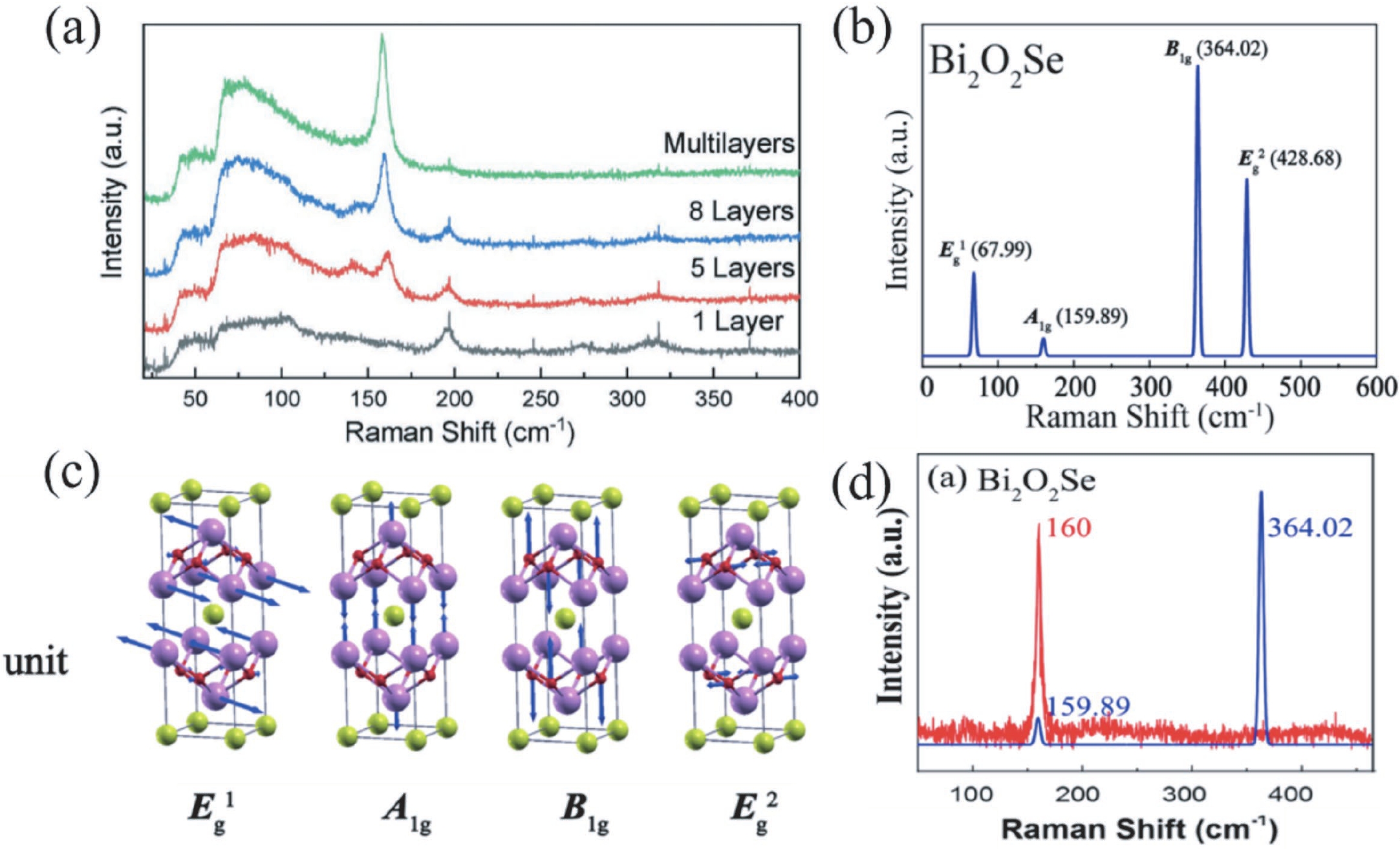
Cheng T, Tan C W, Zhang S Q, et al. Raman spectra and strain effects in bismuth oxychalcogenides. J Phys Chem C, 2018, 122, 19970 doi: 10.1021/acs.jpcc.8b05475 |
| [56] |
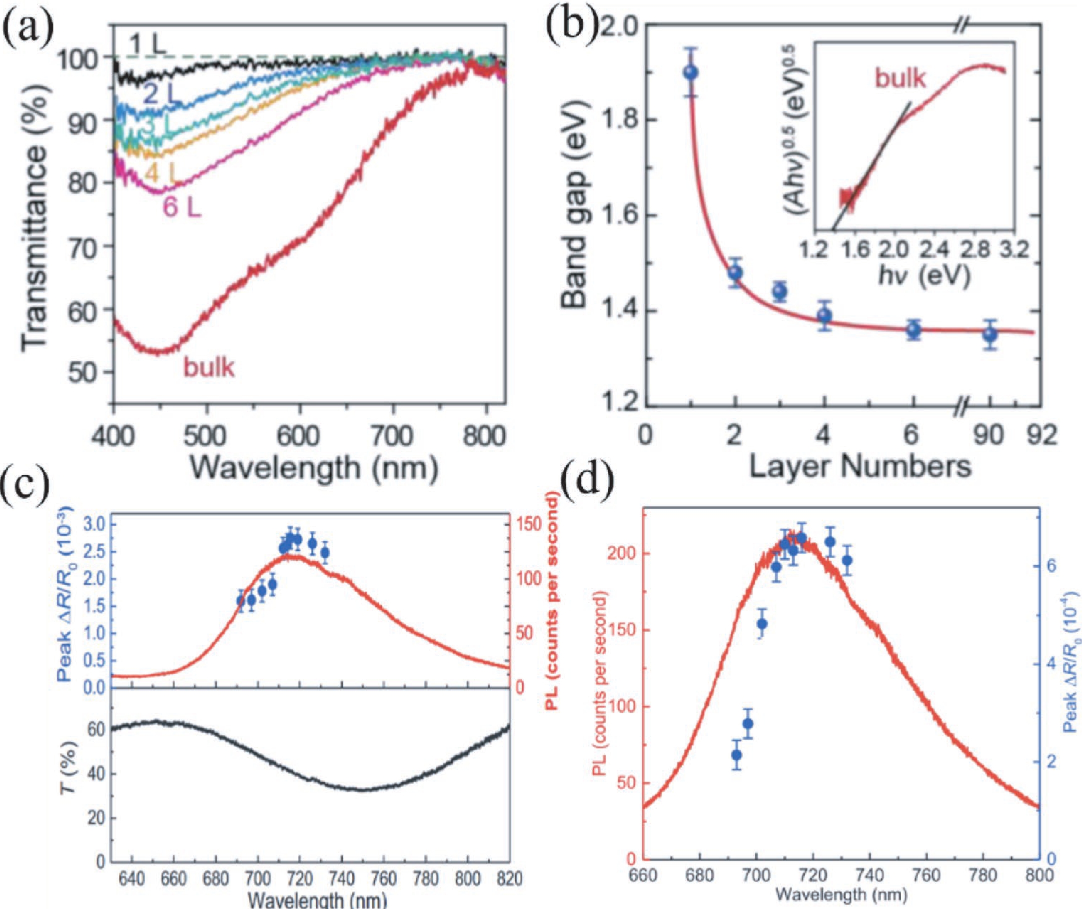
Liu S Y, Tan C W, He D W, et al. Optical properties and photocarrier dynamics of Bi 2O 2Se monolayer and nanoplates. Adv Optical Mater, 2020, 8, 1901567 doi: 10.1002/adom.201901567 |
| [57] |
Zhang Y, Gao Q, Han X Y, et al. Mechanical flexibility and strain engineered-band structures of monolayer Bi 2O 2Se. Phys E, 2020, 116, 113728 doi: 10.1016/j.physe.2019.113728 |
| [58] |
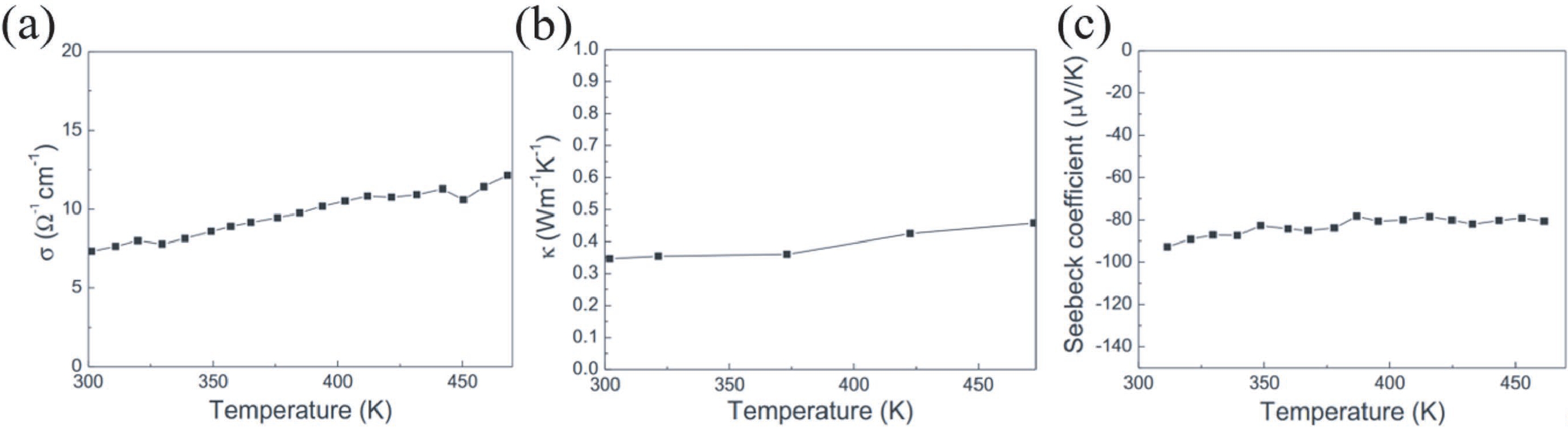
Guo D L, Hu C G, Xi Y, et al. Strain effects to optimize thermoelectric properties of doped Bi 2O 2Se via tran-blaha modified becke-Johnson density functional theory. J Phys Chem C, 2013, 117, 21597 doi: 10.1021/jp4080465 |
| [59] |
|
| [60] |
Yu J B, Sun Q. Bi 2O 2Se nanosheet: An excellent high-temperature n-type thermoelectric material. Appl Phys Lett, 2018, 112, 053901 doi: 10.1063/1.5017217 |
| [61] |
Zhao L D, Lo S H, Zhang Y S, et al. Ultralow thermal conductivity and high thermoelectric figure of merit in SnSe crystals. Nature, 2014, 508, 373 doi: 10.1038/nature13184 |
| [62] |
Yang F, Wang R D, Zhao W W, et al. Thermal transport and energy dissipation in two-dimensional Bi 2O 2Se. Appl Phys Lett, 2019, 115, 193103 doi: 10.1063/1.5123682 |
| [63] |
Yang H, Tan C W, Deng C Y, et al. Bolometric effect in Bi 2O 2Se photodetectors. Small, 2019, 15, e1904482 doi: 10.1002/smll.201904482 |
| [64] |
Konstantatos G, Badioli M, Gaudreau L, et al. Hybrid graphene–quantum dot phototransistors with ultrahigh gain. Nat Nanotechnol, 2012, 7, 363 doi: 10.1038/nnano.2012.60 |
| [65] |
Liu W, Lv J H, Peng L, et al. Graphene charge-injection photodetectors. Nat Electron, 2022, 5, 281 doi: 10.1038/s41928-022-00755-5 |
| [66] |
Wang L, Meric I, Huang P Y, et al. One-dimensional electrical contact to a two-dimensional material. Science, 2013, 342, 614 doi: 10.1126/science.1244358 |
| [67] |
Wu J, Liu Y, Tan Z, et al. Chemical patterning of high-mobility semiconducting 2D Bi 2O 2Se crystals for integrated optoelectronic devices. Adv Mater, 2017, 29, 1704060 doi: 10.1002/adma.201704060 |
| [68] |
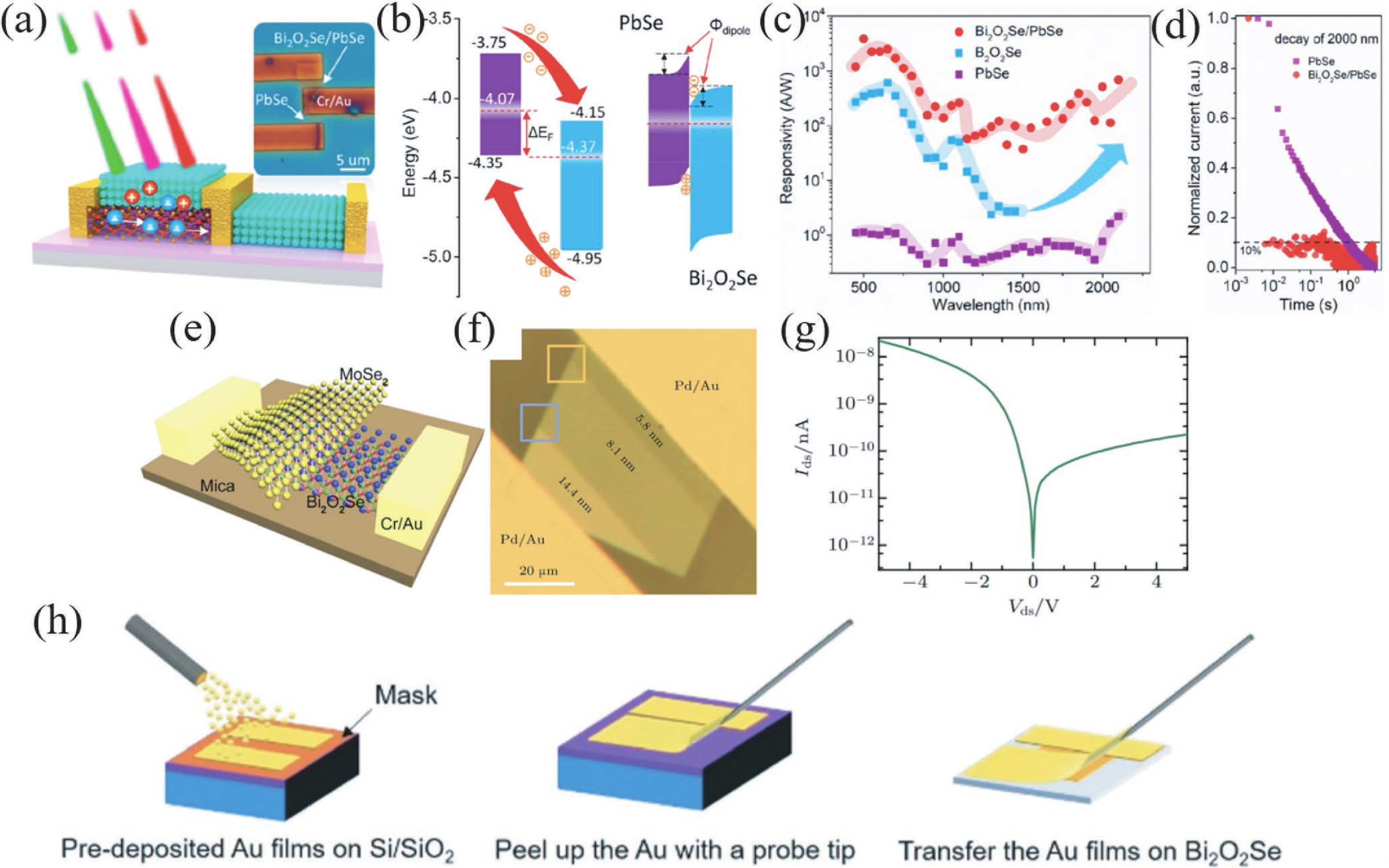
Luo P, Zhuge F W, Wang F K, et al. PbSe quantum dots sensitized high-mobility Bi 2O 2Se nanosheets for high-performance and broadband photodetection beyond 2 μm. ACS Nano, 2019, 13, 9028 doi: 10.1021/acsnano.9b03124 |
| [69] |
Yang H, Chen W, Zheng X M, et al. Near-infrared photoelectric properties of multilayer Bi 2O 2Se nanofilms. Nanoscale Res Lett, 2019, 14, 371 doi: 10.1186/s11671-019-3179-4 |
| [70] |
Yang T, Li X, Wang L M, et al. Broadband photodetection of 2D Bi 2O 2Se-MoSe 2 heterostructure. J Mater Sci, 2019, 54, 14742 doi: 10.1007/s10853-019-03963-1 |
| [71] |
Hong C Y, Huang G F, Yao W W, et al. Thickness-modulated in-plane Bi 2O 2Se homojunctions for ultrafast high-performance photodetectors. Chin Phys B, 2019, 28, 367 doi: 10.1088/1674-1056/ab4e87 |
| [72] |
Liu X L, Li R P, Hong C Y, et al. Highly efficient broadband photodetectors based on lithography-free Au/Bi 2O 2Se/Au heterostructures. Nanoscale, 2019, 11, 20707 doi: 10.1039/C9NR06723J |
| [73] |
Li J, Wang Z X, Chu J W, et al. Oriented layered Bi 2O 2Se nanowire arrays for ultrasensitive photodetectors. Appl Phys Lett, 2019, 114, 151104 doi: 10.1063/1.5094192 |
| [74] |
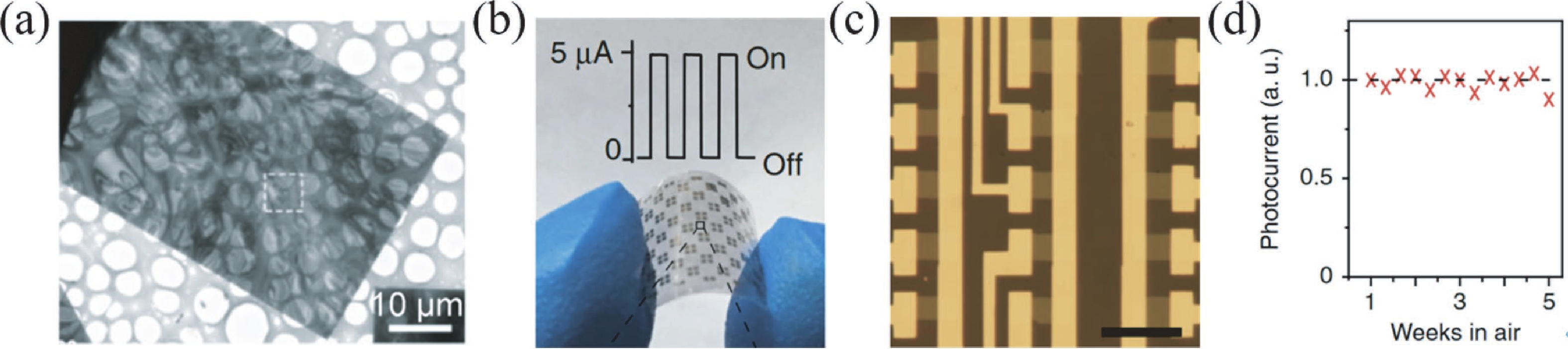
Li D Y, Han X, Xu G Y, et al. Bi 2O 2Se photoconductive detector with low power consumption and high sensitivity. Acta Phys Sin Chin Ed, 2020, 69, 248502 doi: 10.7498/aps.69.20201044 |
| [75] |
Han W, Li C, Yang S J, et al. Atomically thin oxyhalide solar-blind photodetectors. Small, 2020, 16, e2000228 doi: 10.1002/smll.202000228 |
| [76] |
Long M S, Shen Z, Wang R J, et al. Ultrasensitive solar-blind ultraviolet photodetector based on FePSe 3/MoS 2 heterostructure response to 10.6 µm. Adv Funct Mater, 2022, 32, 2204230 doi: 10.1002/adfm.202204230 |
| [77] |
Han X, Xing J, Xu H, et al. Remarkable improved photoelectric performance of SnS 2 field-effect transistor with Au plasmonic nanostructures. Nanotechnology, 2020, 31, 215201 doi: 10.1088/1361-6528/ab72bf |
| [78] |
Xu Y, Ali A, Shehzad K, et al. Photodetectors: Solvent-based soft-patterning of graphene lateral heterostructures for broadband high-speed metal-semiconductor-metal photodetectors. Adv Mater Technol, 2017, 2, 1600241 doi: 10.1002/admt.201600241 |
| [79] |
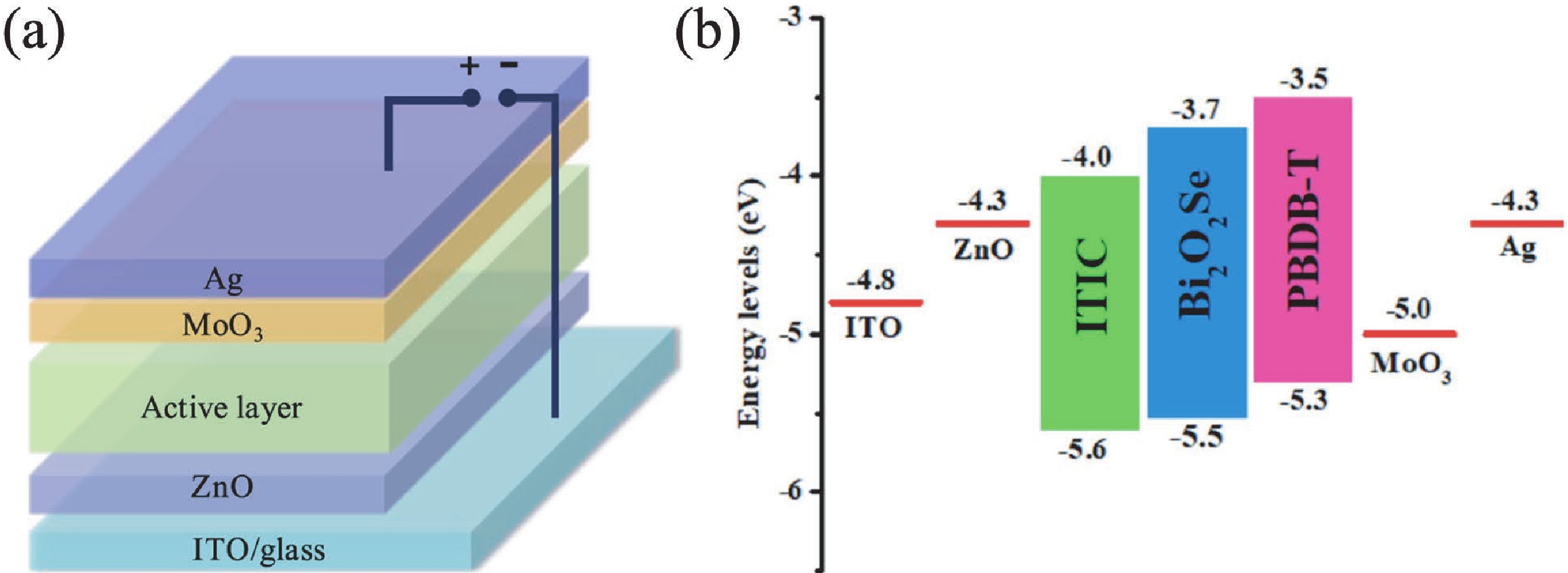
Huang C W, Yu H. 2D Bi 2O 2Se with high mobility for high performance polymer solar cells. ACS Appl Mater Interfaces, 2020, 12, 19643 doi: 10.1021/acsami.0c01364 |
| [80] |
Ding G L, Yang B D, Chen R S, et al. Reconfigurable 2D WSe 2-based memtransistor for mimicking homosynaptic and heterosynaptic plasticity. Small, 2021, 17, 2170213 doi: 10.1002/smll.202170213 |
| [81] |
Du J Y, Ge C, Riahi H, et al. Dual-gated MoS 2 transistors for synaptic and programmable logic functions. Adv Electron Mater, 2020, 6, 1901408 doi: 10.1002/aelm.201901408 |
| [82] |
Yang Q Y, Luo Z D, Zhang D W, et al. Controlled optoelectronic response in van der Waals heterostructures for In-sensor computing. Adv Funct Mater, 2022, 32(45), 202207290 doi: 10.1002/adfm.202207290 |
| [83] |
Yan J M, Ying J S, Yan M Y, et al. Optoelectronic coincidence detection with two-dimensional Bi 2O 2Se ferroelectric field-effect transistors. Adv Funct Mater, 2021, 31, 2103982 doi: 10.1002/adfm.202103982 |
| [84] |
Wang F K, Yang S J, Wu J, et al. Emerging two-dimensional bismuth oxychalcogenides for electronics and optoelectronics. InfoMat, 2021, 3, 1251 doi: 10.1002/inf2.12215 |
| [85] |
Li Z W, Li J S. Bi 2O 2Se for broadband terahertz wave switching. Appl Opt, 2020, 59, 11076 doi: 10.1364/AO.412728 |
| [86] |
Meng X D, Liu Z Q, Cao Y, et al. Cancer therapy: Fabricating aptamer-conjugated PEGylated-MoS 2/Cu 1.8S theranostic nanoplatform for multiplexed imaging diagnosis and chemo-photothermal therapy of cancer. Adv Funct Mater, 2017, 27, 1605592 doi: 10.1002/adfm.201605592 |
| [87] |
Chen Z, Zhao P F, Luo Z Y, et al. Cancer cell membrane-biomimetic nanoparticles for homologous-targeting dual-modal imaging and photothermal therapy. ACS Nano, 2016, 10, 10049 doi: 10.1021/acsnano.6b04695 |
| [88] |
Li B, Yuan F K, He G J, et al. Ultrasmall CuCo 2S 4 nanocrystals: All-in-one theragnosis nanoplatform with magnetic resonance/near-infrared imaging for efficiently photothermal therapy of tumors. Adv Funct Mater, 2017, 27, 1606218 doi: 10.1002/adfm.201606218 |
| [89] |
Wu M H, Zeng X C. Bismuth oxychalcogenides: A new class of ferroelectric/ferroelastic materials with ultra high mobility. Nano Lett, 2017, 17, 6309 doi: 10.1021/acs.nanolett.7b03020 |
| [90] |
Zhu Z Y, Yao X P, Zhao S, et al. Giant modulation of the electron mobility in semiconductor Bi 2O 2Se via incipient ferroelectric phase transition. J Am Chem Soc, 2022, 144, 4541 doi: 10.1021/jacs.1c12681 |


 DownLoad:


 Huayu Tao:is an undergraduate in the School of Materials Science and Engineering of China University of Geosciences (Beijing), mainly engaged in the research of low dimensional oxide materials. Her work has been published in Renewable & Sustainable Energy Reviews
 Gengwei Li:has worked in China University of Geosciences (Beijing) since he graduated from Beijing Normal University with a master's degree in optics in 2001, and received a doctorate in solid geophysics from China University of Geosciences (Beijing) in 2013. Mainly engaged in the theoretical research of optics, thin film materials and electromagnetic fields. Nearly 50 papers have been published, including Materials Research Express, Acta Physica Sinica, Materials Review, OptoElectronics Letters, etc


