


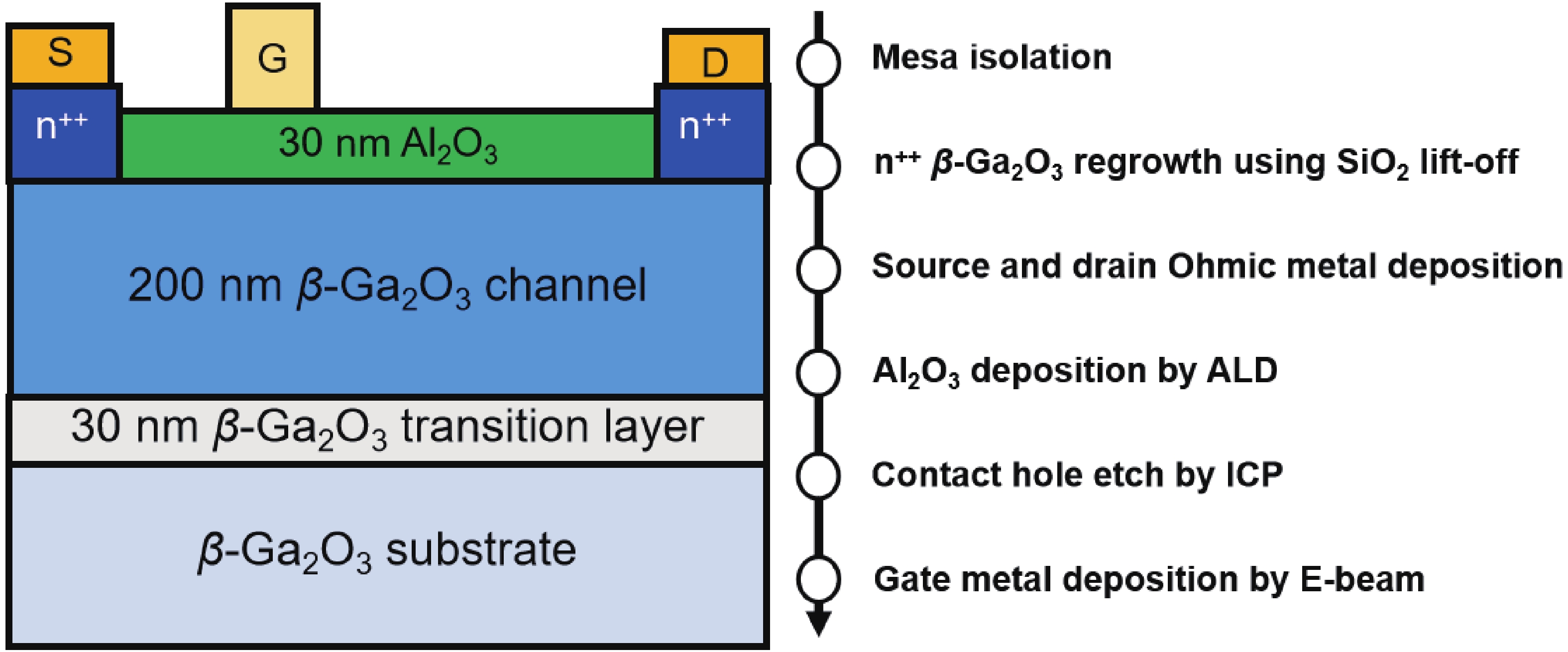
Fig. 1.
(Color online) Cross-sectional schematic of the β-Ga2O3 MOSFET and its process flow.
ARTICLES
Xuanze Zhou, Guangwei Xu and Shibing Long
Corresponding author: Guangwei Xu, xugw@ustc.edu.cn; Shibing Long, shibinglong@ustc.edu.cn
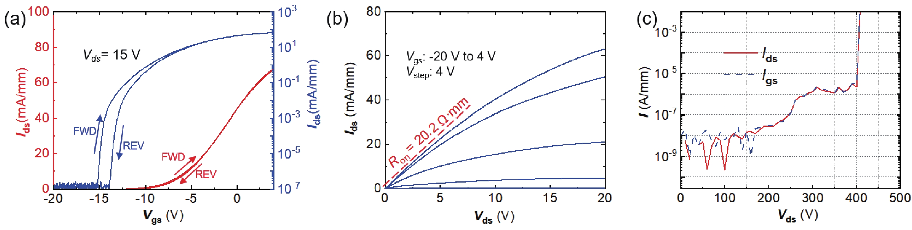
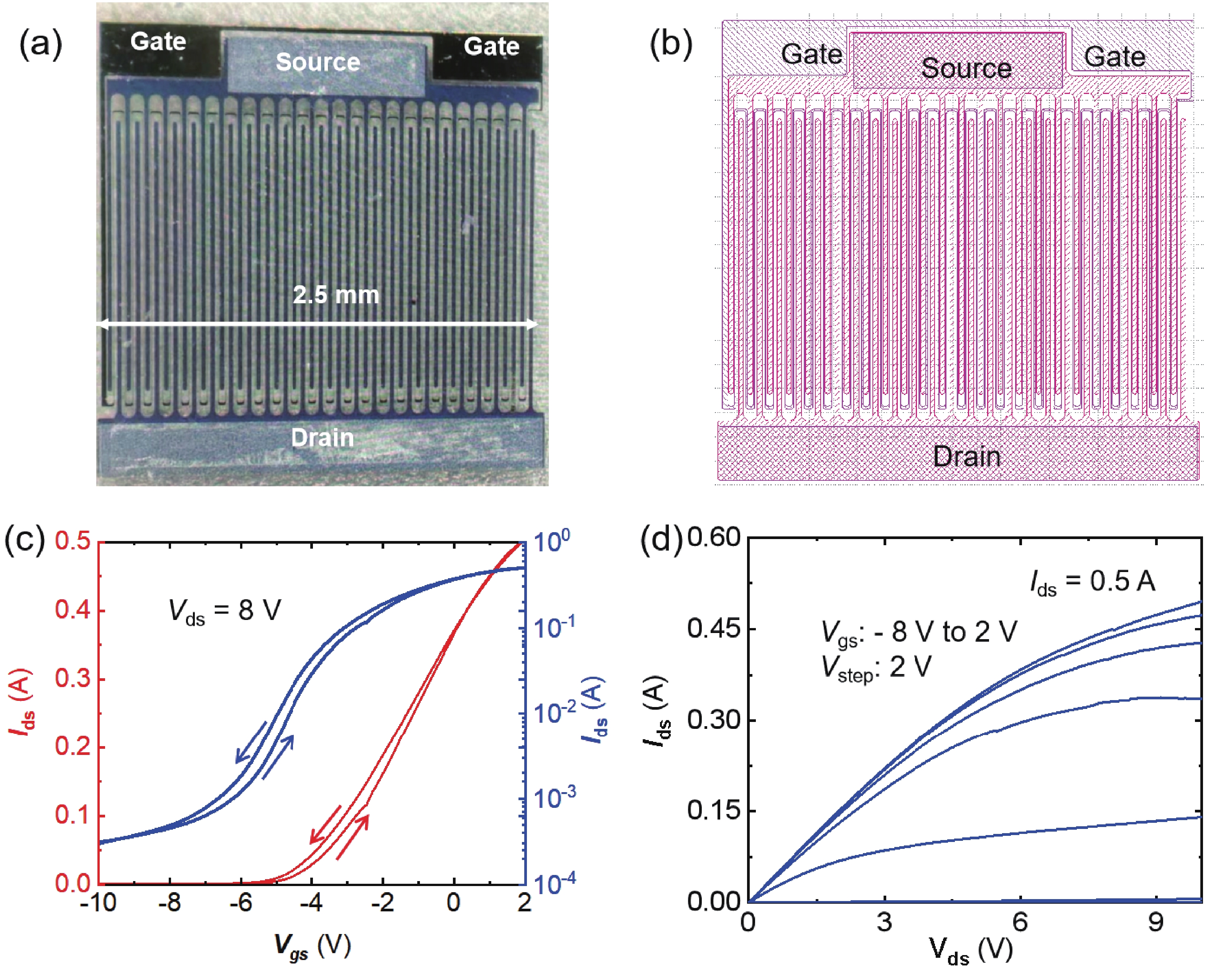
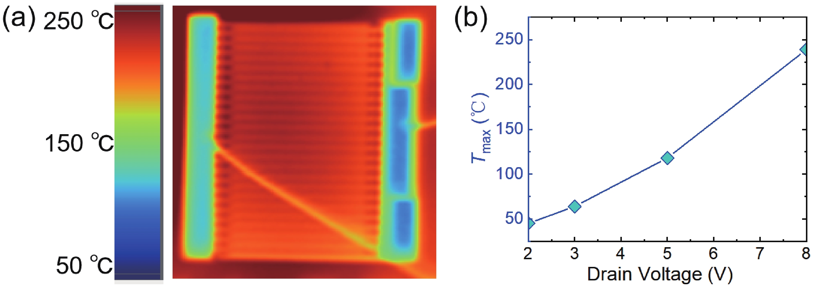
Abstract: The self-heating effect severely limits device performance and reliability. Although some studies have revealed the heat distribution of β-Ga2O3 MOSFETs under biases, those devices all have small areas and have difficulty reflecting practical conditions. This work demonstrated a multi-finger β-Ga2O3 MOSFET with a maximum drain current of 0.5 A. Electrical characteristics were measured, and the heat dissipation of the device was investigated through infrared images. The relationship between device temperature and time/bias is analyzed.
Keywords: β-Ga2O3, MOSFET, multi-finger, self-heating effect
| [1] |
Higashiwaki M, Sasaki K, Murakami H, et al. Recent progress in Ga2O3 power devices. Semicond Sci Technol, 2016, 31, 034001 doi: 10.1088/0268-1242/31/3/034001
|
| [2] |
Dong H, Xue H W, He Q M, et al. Progress of power field effect transistor based on ultra-wide bandgap Ga2O3 semiconductor material. J Semicond, 2019, 40, 011802 doi: 10.1088/1674-4926/40/1/011802
|
| [3] |
Kuramata A, Koshi K, Watanabe S, et al. High-quality β-Ga2O3 single crystals grown by edge-defined film-fed growth. Jpn J Appl Phys, 2016, 55, 1202A2 doi: 10.7567/JJAP.55.1202A2
|
| [4] |
Tomm Y, Reiche P, Klimm D, et al. Czochralski grown Ga2O3 crystals. J Cryst Growth, 2000, 220, 510 doi: 10.1016/S0022-0248(00)00851-4
|
| [5] |
Yu Y T, Xiang X Q, Zhou X Z, et al. Device topological thermal management of β-Ga2O3 Schottky barrier diodes. Chin Phys B, 2021, 30, 067302 doi: 10.1088/1674-1056/abeee2
|
| [6] |
Higashiwaki M, Sasaki K, Kuramata A, et al. Gallium oxide (Ga2O3) metal-semiconductor field-effect transistors on single-crystal β-Ga2O3 (010) substrates. Appl Phys Lett, 2012, 100, 013504 doi: 10.1063/1.3674287
|
| [7] |
Liu H Y, Li J N, Lv Y J, et al. Improved electrical performance of lateral β-Ga2O3 MOSFETs utilizing slanted fin channel structure. Appl Phys Lett, 2022, 121, 202101 doi: 10.1063/5.0119694
|
| [8] |
Bhattacharyya A, Ranga P, Roy S, et al. Multi-kV class β-Ga2O3 MESFETs with a lateral figure of merit up to 355 MW/cm². IEEE Electron Device Lett, 2021, 42, 1272 doi: 10.1109/LED.2021.3100802
|
| [9] |
Zhou X Z, Ma Y J, Xu G W, et al. Enhancement-mode β-Ga2O3 U-shaped gate trench vertical MOSFET realized by oxygen annealing. Appl Phys Lett, 2022, 121, 223501 doi: 10.1063/5.0130292
|
| [10] |
Wang C L, Zhou H, Zhang J C, et al. Hysteresis-free and μs-switching of D/E-modes Ga2O3 hetero-junction FETs with the BV2/Ron, sp of 0.74/0.28 GW/cm2. Appl Phys Lett, 2022, 120, 112101 doi: 10.1063/5.0084804
|
| [11] |
Zhou X, Liu Q, Hao W, et al. Normally-off β-Ga2O3 power heterojunction fieldeffect-transistor realized by p-NiO and recessed gate. IEEE 26th Int Symp Power Semiconductor Devices IC’s (ISPSD), 2022 doi: 10.1109/ISPSD49238.2022.9813678
|
| [12] |
Kim S, Zhang Y W, Yuan C, et al. Thermal management of β-Ga2O3 current aperture vertical electron transistors. IEEE Trans Compon, Packag Manufact Technol, 2021, 11, 1171 doi: 10.1109/TCPMT.2021.3089321
|
| [13] |
Chatterjee B, Zeng K, Nordquist C D, et al. Device-level thermal management of gallium oxide field-effect transistors. IEEE Trans Compon Packag Manuf Technol, 2019, 9, 2352 doi: 10.1109/TCPMT.2019.2923356
|
| [14] |
Xu W H, Wang Y B, You T G, et al. First demonstration of waferscale heterogeneous integration of Ga2O3 MOSFETs on SiC and Si substrates by ion-cutting process. 2019 IEEE International Electron Devices Meeting (IEDM), 2019, 12 doi: 10.1109/IEDM19573.2019.8993501
|
| [15] |
Noh J, Alajlouni S, Tadjer M J, et al. High performance β-Ga2O3 nano-membrane field effect transistors on a high thermal conductivity diamond substrate. IEEE J Electron Devices, 2019, 7, 914 doi: 10.1109/JEDS.2019.2933369
|
| [16] |
Zhou H, Maize K, Noh J, et al. Thermodynamic studies of Ga2O3 nanomembrane field-effect transistors on a sapphire substrate. ACS Omega, 2017, 2, 7723 doi: 10.1021/acsomega.7b01313
|
| [17] |
Chatterjee B, Li W, Nomoto K, et al. Thermal design of multi-fin Ga2O3 vertical transistors. Appl Phys Lett, 2021, 119, 103502 doi: 10.1063/5.0056557
|
| [18] |
Kumar N, Vaca D, Joishi C, et al. Ultrafast thermoreflectance imaging and electrothermal modeling of β-Ga2O3 MESFETs. IEEE Electron Device Lett, 2020, 41, 641 doi: 10.1109/LED.2020.2975038
|
| [19] |
Böcker J, Tetzner K, Heucke S, et al. Dispersion effects in on-state resistance of lateral Ga2O3 MOSFETs at 300 V switching. Electon Lett, 2020, 56, 838 doi: 10.1049/el.2020.1286
|
| [20] |
Gong H H, Zhou F, Yu X X, et al. 70-μm-body Ga2O3 Schottky barrier diode with 1.48 K/W thermal resistance, 59 A surge current and 98.9% conversion efficiency. IEEE Electron Device Lett, 2022, 43, 773 doi: 10.1109/LED.2022.3162393
|


Article views: 2473 Times PDF downloads: 272 Times Cited by: 0 Times
Received: 31 December 2022 Revised: 20 February 2023 Online: Accepted Manuscript: 14 March 2023Uncorrected proof: 16 March 2023Corrected proof: 07 June 2023Published: 10 July 2023
| Citation: |
Xuanze Zhou, Guangwei Xu, Shibing Long. A large-area multi-finger β-Ga2O3 MOSFET and its self-heating effect[J]. Journal of Semiconductors, 2023, 44(7): 072804. doi: 10.1088/1674-4926/44/7/072804
****
X Z Zhou, G W Xu, S B Long. A large-area multi-finger β-Ga2O3 MOSFET and its self-heating effect[J]. J. Semicond, 2023, 44(7): 072804. doi: 10.1088/1674-4926/44/7/072804

|
 Xuanze Zhou:got his BS from Nanchang University in 2018. Now he is a PhD student at University of Science and Technology of China under the supervision of Prof. Shibing Long and Dr. Guangwei Xu. His research focuses on gallium oxide power MOSFETs
 Guangwei Xu:received his PhD from the Institute of Microelectronics of the Chinese Academy of Sciences in 2017. Then, he joined the University of California, Los Angeles as a postdoc. He joined the University of Science and Technology of China as an associate research fellow in the Shibing Long Group in 2019. His research focuses on wide bandgap semiconductor power device fabrication, device defect state measurement and device modeling
 Shibing Long:is a full professor at the Institute of Microelectronics, University of Science and Technology of China. He received his PhD from the Institute of Microelectronics of the Chinese Academy of Sciences in 2005. Then, he worked there from 2005 to 2018 and joined the University of Science and Technology of China in 2018. His research focuses on micro- and nanofabrication, RRAM, ultrawide bandgap semiconductor devices (power devices and detectors) and memory circuit design
| [1] |
Higashiwaki M, Sasaki K, Murakami H, et al. Recent progress in Ga2O3 power devices. Semicond Sci Technol, 2016, 31, 034001 doi: 10.1088/0268-1242/31/3/034001
|
| [2] |
Dong H, Xue H W, He Q M, et al. Progress of power field effect transistor based on ultra-wide bandgap Ga2O3 semiconductor material. J Semicond, 2019, 40, 011802 doi: 10.1088/1674-4926/40/1/011802
|
| [3] |
Kuramata A, Koshi K, Watanabe S, et al. High-quality β-Ga2O3 single crystals grown by edge-defined film-fed growth. Jpn J Appl Phys, 2016, 55, 1202A2 doi: 10.7567/JJAP.55.1202A2
|
| [4] |
Tomm Y, Reiche P, Klimm D, et al. Czochralski grown Ga2O3 crystals. J Cryst Growth, 2000, 220, 510 doi: 10.1016/S0022-0248(00)00851-4
|
| [5] |
Yu Y T, Xiang X Q, Zhou X Z, et al. Device topological thermal management of β-Ga2O3 Schottky barrier diodes. Chin Phys B, 2021, 30, 067302 doi: 10.1088/1674-1056/abeee2
|
| [6] |
Higashiwaki M, Sasaki K, Kuramata A, et al. Gallium oxide (Ga2O3) metal-semiconductor field-effect transistors on single-crystal β-Ga2O3 (010) substrates. Appl Phys Lett, 2012, 100, 013504 doi: 10.1063/1.3674287
|
| [7] |
Liu H Y, Li J N, Lv Y J, et al. Improved electrical performance of lateral β-Ga2O3 MOSFETs utilizing slanted fin channel structure. Appl Phys Lett, 2022, 121, 202101 doi: 10.1063/5.0119694
|
| [8] |
Bhattacharyya A, Ranga P, Roy S, et al. Multi-kV class β-Ga2O3 MESFETs with a lateral figure of merit up to 355 MW/cm². IEEE Electron Device Lett, 2021, 42, 1272 doi: 10.1109/LED.2021.3100802
|
| [9] |
Zhou X Z, Ma Y J, Xu G W, et al. Enhancement-mode β-Ga2O3 U-shaped gate trench vertical MOSFET realized by oxygen annealing. Appl Phys Lett, 2022, 121, 223501 doi: 10.1063/5.0130292
|
| [10] |
Wang C L, Zhou H, Zhang J C, et al. Hysteresis-free and μs-switching of D/E-modes Ga2O3 hetero-junction FETs with the BV2/Ron, sp of 0.74/0.28 GW/cm2. Appl Phys Lett, 2022, 120, 112101 doi: 10.1063/5.0084804
|
| [11] |
Zhou X, Liu Q, Hao W, et al. Normally-off β-Ga2O3 power heterojunction fieldeffect-transistor realized by p-NiO and recessed gate. IEEE 26th Int Symp Power Semiconductor Devices IC’s (ISPSD), 2022 doi: 10.1109/ISPSD49238.2022.9813678
|
| [12] |
Kim S, Zhang Y W, Yuan C, et al. Thermal management of β-Ga2O3 current aperture vertical electron transistors. IEEE Trans Compon, Packag Manufact Technol, 2021, 11, 1171 doi: 10.1109/TCPMT.2021.3089321
|
| [13] |
Chatterjee B, Zeng K, Nordquist C D, et al. Device-level thermal management of gallium oxide field-effect transistors. IEEE Trans Compon Packag Manuf Technol, 2019, 9, 2352 doi: 10.1109/TCPMT.2019.2923356
|
| [14] |
Xu W H, Wang Y B, You T G, et al. First demonstration of waferscale heterogeneous integration of Ga2O3 MOSFETs on SiC and Si substrates by ion-cutting process. 2019 IEEE International Electron Devices Meeting (IEDM), 2019, 12 doi: 10.1109/IEDM19573.2019.8993501
|
| [15] |
Noh J, Alajlouni S, Tadjer M J, et al. High performance β-Ga2O3 nano-membrane field effect transistors on a high thermal conductivity diamond substrate. IEEE J Electron Devices, 2019, 7, 914 doi: 10.1109/JEDS.2019.2933369
|
| [16] |
Zhou H, Maize K, Noh J, et al. Thermodynamic studies of Ga2O3 nanomembrane field-effect transistors on a sapphire substrate. ACS Omega, 2017, 2, 7723 doi: 10.1021/acsomega.7b01313
|
| [17] |
Chatterjee B, Li W, Nomoto K, et al. Thermal design of multi-fin Ga2O3 vertical transistors. Appl Phys Lett, 2021, 119, 103502 doi: 10.1063/5.0056557
|
| [18] |
Kumar N, Vaca D, Joishi C, et al. Ultrafast thermoreflectance imaging and electrothermal modeling of β-Ga2O3 MESFETs. IEEE Electron Device Lett, 2020, 41, 641 doi: 10.1109/LED.2020.2975038
|
| [19] |
Böcker J, Tetzner K, Heucke S, et al. Dispersion effects in on-state resistance of lateral Ga2O3 MOSFETs at 300 V switching. Electon Lett, 2020, 56, 838 doi: 10.1049/el.2020.1286
|
| [20] |
Gong H H, Zhou F, Yu X X, et al. 70-μm-body Ga2O3 Schottky barrier diode with 1.48 K/W thermal resistance, 59 A surge current and 98.9% conversion efficiency. IEEE Electron Device Lett, 2022, 43, 773 doi: 10.1109/LED.2022.3162393
|

 WeChat ID
Journal of Semiconductors © 2017 All Rights Reserved 京ICP备05085259号-2

 DownLoad:

