Processing math: 100%
J. Semicond. > 2023, Volume 44 > Issue 7 > 074101

ARTICLES

Amorphous gallium oxide homojunction-based optoelectronic synapse for multi-functional signal processing

Rongliang Li1, Yonghui Lin1, Yang Li1, 2, , Song Gao1, Wenjing Yue1, Hao Kan1, Chunwei Zhang1 and Guozhen Shen3,

+ Author Affiliations

 Corresponding author: Yang Li, yang.li@sdu.edu.cn; Guozhen Shen, gzshen@bit.edu.cn

DOI: 10.1088/1674-4926/44/7/074101

PDF

Turn off MathJax

Abstract: In the era of accelerated development in artificial intelligence as well as explosive growth of information and data throughput, underlying hardware devices that can integrate perception and memory while simultaneously offering the benefits of low power consumption and high transmission rates are particularly valuable. Neuromorphic devices inspired by the human brain are considered to be one of the most promising successors to the efficient in-sensory process. In this paper, a homojunction-based multi-functional optoelectronic synapse (MFOS) is proposed and testified. It enables a series of basic electrical synaptic plasticity, including paired-pulse facilitation/depression (PPF/PPD) and long-term promotion/depression (LTP/LTD). In addition, the synaptic behaviors induced by electrical signals could be instead achieved through optical signals, where its sensitivity to optical frequency allows the MFOS to simulate high-pass filtering applications in situ and the perception capability integrated into memory endows it with the information acquisition and processing functions as a visual system. Meanwhile, the MFOS exhibits its performances of associative learning and logic gates following the illumination with two different wavelengths. As a result, the proposed MFOS offers a solution for the realization of intelligent visual system and bionic electronic eye, and will provide more diverse application scenarios for future neuromorphic computing.

Key words: optoelectronic synapsegallium oxidefiltervisual systemassociative learninglogic gate

Artificial intelligence and the Internet of Things have gradually developed and grown with the advancement of technology, and are now taking shape on a massive scale. However, compared to the software and algorithms, the progression of underlying hardware devices suffers from a non-negligible lag[1-3]. The von Neumann architecture and computing paradigm, which separate the memory and computation, is running out of steam as Moore’s Law tends to the end. It makes traditional hardware systems unable to meet the increasing demands on power consumption and efficiency[4, 5]. With the emergence of brain-like neuromorphic devices, the technical barrier of discrete functional units mentioned above seems to be overcome. In biology, approximately 86 billion neurons and 1015 synapses are distributed throughout the brain and connected to form an extremely vast and complicated biological neural network[6-8]. Neural networks empower the brain to learn and process information efficiently, thereby enabling the interaction between organisms and the external environment at very low power consumption and supporting the human functions related to perception and memory[9-11]. Given that 80% of the external information received by the brain comes from the eyes, the implementation of an artificial visual system seems to be necessary, which inspires the exploitation of bionic visual systems through electronic devices for future artificial visual computing[12-13].

However, traditional bionic visual systems consist of image sensors and artificial synaptic devices. In sensor-rich applications including intelligent vehicles, static or dynamic video analysis, and micro-robots, the massive amount of raw data collected locally by the sensing terminal must be transferred to local storage and computing units or cloud-based systems, where the inevitable data migration will lead to high power consumption, low processing speed, wide communication bandwidth, and even low security[14-16]. Some optoelectronic devices have been developed to solve the above issues and implement a wide variety of functions in many directions, such as bionic visual receptors[17, 18], filters[19, 20], image recognition[21, 22], polarization-sensitive neuromorphic behavior[23], and motion tracking[24, 25], and they offer excellent performance and the ability to implement the corresponding applications outstandingly. While most devices can only handle a single task and little exploration of multiple functions has been carried out, which greatly limits the potential of the device and the range of its applications. Therefore, it is urgent to explore a perception-memory integrated device for multi-functional processing[26, 27].

Herein, a homojunction-based multi-functional optoelectronic synapse (MFOS) fabricated by magnetron sputtering is prepared and verified. Top electrode Al, intermediate dielectric layer of oxygen-deficient and oxygen-rich gallium oxide (Ga2O3(OD)/Ga2O3(OR)) and bottom electrode ITO are stacked to form a vertical device for implementing electrical and optical synaptic behavior as well as superior optical application. The MFOS realizes basic synaptic functions, including paired-pulse facilitation/depression (PPF/PPD) and long-term promotion/depression (LTP/LTD). Immediately afterward, similar synaptic behaviors are recapitulated with the induction of light signals. Based on the sensitivity of MFOS to optical frequency, the application of high-pass filters can be completed. Meanwhile, the changing light signals are applied to verify the perception-memory integrated visual system. Moreover, a classic example of associative learning of Pavlovian conditioning reflex experience is realized under co-modulation with dual-band wavelength illumination. Similarly, the logic gate of IMP is finally implemented with the read voltage switches to the positive. In brief, the all-in-one optoelectronic devices are expected to improve the perception and processing efficiency of the artificial visual system and enrich the application scenarios for future neuromorphic computing.

ITO-coated glass substrates were purchased from Yingkou OPV Tech New Energy Co., Ltd. The commercially Ga2O3 target (99.999%) was purchased from Beijing Zhongnuo Advanced Materials Technology Co., Ltd.

The optoelectronic synapse was fabricated on a transparent glass substrate covered with ITO. Before deposition, the substrate was cleaned ultrasonically in the sequence of acetone, ethanol, and deionized (DI) water. And the ITO substrate was positioned in the vacuum sputtering chamber to deposit the Ga2O3(OD) and Ga2O3(OR) film in order by the RF magnetron sputtering process. The pressure was initially controlled at 3.6 × 10⁻³ Pa and then increased to 1 Pa by introducing argon gas at a flow rate of 20 sccm. The operating power was always set at 80 W. After sputtering for 30 min, the oxygen gas at a flow rate of 5 sccm was fed into the vacuum sputtering chamber and the flow rate of argon gas was changed to 15 sccm. Sputtering for another 30 min, the ITO/Ga2O3(OD)/Ga2O3(OR) was prepared. Finally, top Al electrodes with a diameter of 400 µm were deposited via direct-current magnetron sputtering to complete the ITO/Ga2O3(OD)/Ga2O3(OR)/Al-based device.

The cross-sectional image of the MFOS was taken using the field-emission SEM and EDS (Regulus-8100, Hitachi, Japan). The crystalline structures of the Ga2O3(OD) and Ga2O3(OR) are analyzed by an XRD (Bruker D8 Advance). XPS (AXIS SUPRA, Kratos) was carried out to confirm the chemical composition and the position of their valence band of the Ga2O3(OD) and Ga2O3(OR) films. UPS (1UPSHeI light source (21.22 eV)) was carried out to ensure the position of their fermi level. The absorbance spectra of the film were measured by a UV-vis spectrophotometer (EVOLUTION 201, Thermo Scientific Corporation). The electrical performance and synaptic functions of MFOS were performed on semiconductor parameter analyzers (Keithley 2602B and B1500A) connected to a probe station in ambient conditions. The ultraviolet (UV) LED light sources (254 ± 10 and 365 ± 10 nm) were used during the light-induced measurements. The UV pulses were generated by a function generator (SPF80, Nanjing Shengpu instrument) and the UV light intensity was calibrated by a UV LIGHT METER (PM100USB, THORLABS).

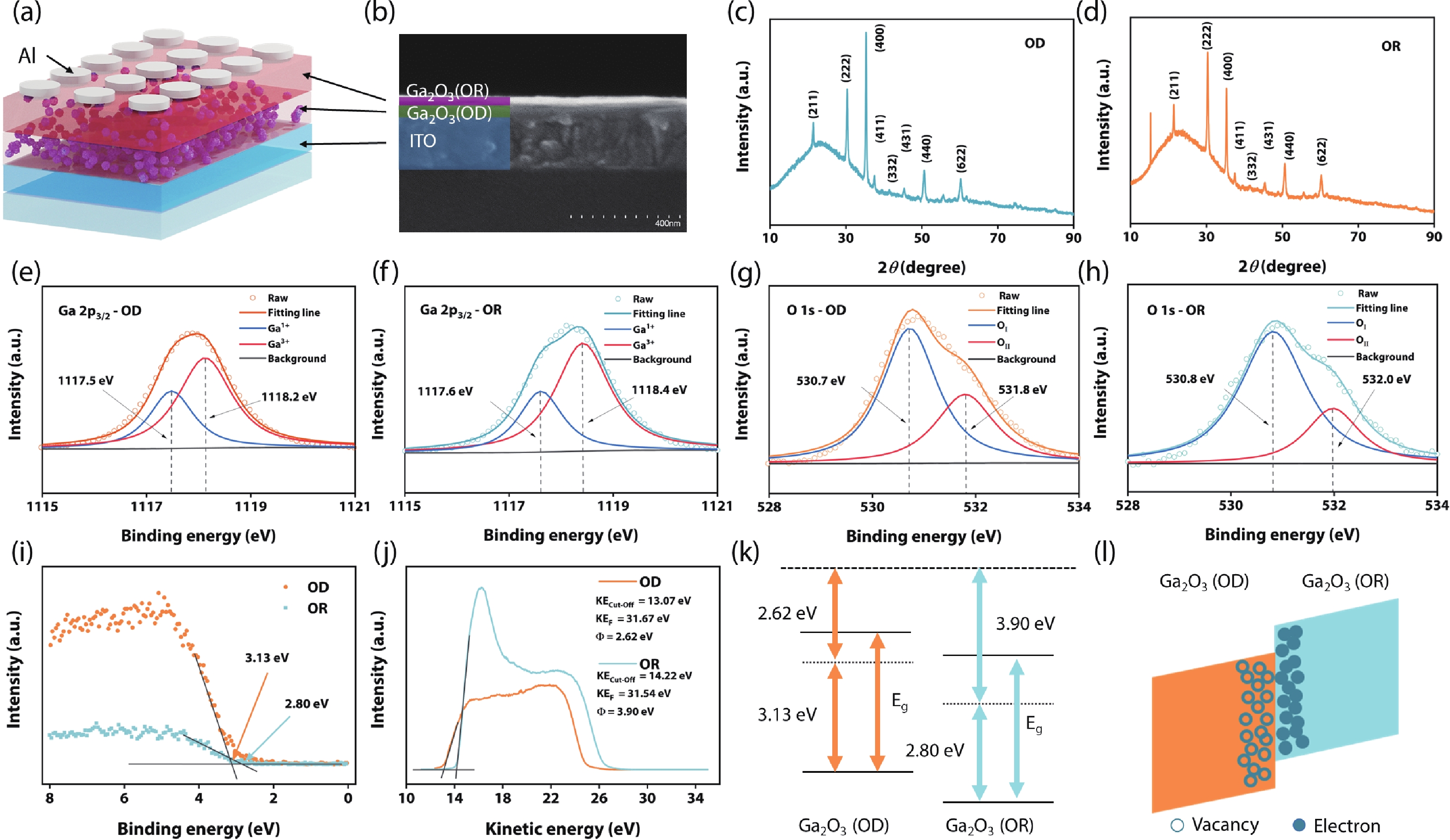
As illustrated in the schematic diagram of Fig. 1(a), the device is composed of a top electrode (Al), dielectric layer (Ga2O3(OD) and Ga2O3(OR)), and bottom electrode (ITO) on the glass substrate. And the elements (Ga, O, In, and Sn) distribution in the whole device is testified by EDS spectra, which is shown in Fig. S1 (Supplementary Material). The two films in the dielectric layer are stacked with thicknesses around 50 and 40 nm, and due to the variation of sputtering conditions during preparation, the clear boundary can be observed from the cross-sectional sweeping electron microscopes (SEM) image in Fig. 1(b). In addition, characterizing the crystallinity by X-ray diffractometer (XRD) spectra in Figs. 1(c) and 1(d), the main peaks such as (211), (222), (400), (411), (332), (431), (440), and (622) are mostly resulting from ITO, illustrating that the Ga2O3(OD) and Ga2O3(OR) films are almost amorphous[28]. The planar SEM images exhibit high surface flatness, as shown in Fig. S2 (Supplementary Material), the large particle clusters in Ga2O3(OR) (prepared in the Ar and O2 coexistence atmosphere) are visibly more numerous than those in Ga2O3(OD) (prepared in the pure Ar atmosphere)[29, 30]. To evaluate the internal differences between the dielectric layer films, the X-ray photoelectron spectroscopies (XPS) spectra are measured systematically. The Ga 2p3/2 peak in both films is split into Ga1+ (1117.5 eV in Ga2O3(OD), 1117.6 eV in Ga2O3(OR)) and Ga3+ (1118.2 eV in Ga2O3(OD), 1118.4 eV in Ga2O3(OR)), which correspond to Ga2O and Ga2O3, respectively. As exhibited in Figs. 1(e) and 1(f), the larger Ga3+ peak area indicates that the oxidization of the Ga element in Ga2O3(OR) is more adequate than that in Ga2O3(OD)[31]. This differential oxidation phenomenon is also reflected in O 1s in Figs. 1(g) and 1(h). Split O and O which are related to lattice oxygen and oxygen vacancies take up the content in distinct manners. It can be seen that there are more oxygen vacancies scattered in Ga2O3(OD) than in Ga2O3(OR), which is consistent with the previously analyzed result of deficiently oxidized Ga3+ in Ga2O3(OD), namely, oxygen atmosphere in the sputtering process can effectively increase the oxygen concentration of the gallium oxide film. With the varying gas atmosphere during preparation, the position will differ between the films’ energy bands. As depicted in Fig. 1(i), the valence XPS spectra are measured to calculate the valence band position, where the intersection of the horizontal extension and the oblique tangent of the data points is 3.13 and 2.80 eV for Ga2O3(OD) and Ga2O3(OR), respectively. A method for determining fermi level is drawing support from ultraviolet photo-electron spectroscopy (UPS) spectra depicted in Fig. 1(j). Given the photon energy is 21.22 eV, the work functions (Φ) are calculated to be 2.62 and 3.90 eV for Ga2O3(OD) and Ga2O3(OR), respectively. And a type-Ⅱ homogeneous energy band structure is demonstrated in Fig. 1(k). In conjunction with the above analytical results, the schematic of carrier distribution is depicted in Fig. 1(l). The oxygen vacancies and free electrons converge at the interface of Ga2O3(OD)/Ga2O3(OR), and finally, the homojunction dielectric layer is formed[31, 32].

Fig. 1.  (Color online) (a) The schematic diagram and (b) the cross-sectional SEM image of the device. The XRD spectra of (c) Ga2O3(OD) and (d) Ga2O3(OR). The XPS spectra of (e, f) Ga 2p3/2 peak, as well as (g, h) O 1s peak in two different oxygen-content films. (i) The valence band XPS spectra and (j) UPS spectra of Ga2O3(OD) and Ga2O3(OR). (k) The energy band diagrams and (l) schematic of carrier distribution of Ga2O3(OD) and Ga2O3(OR).

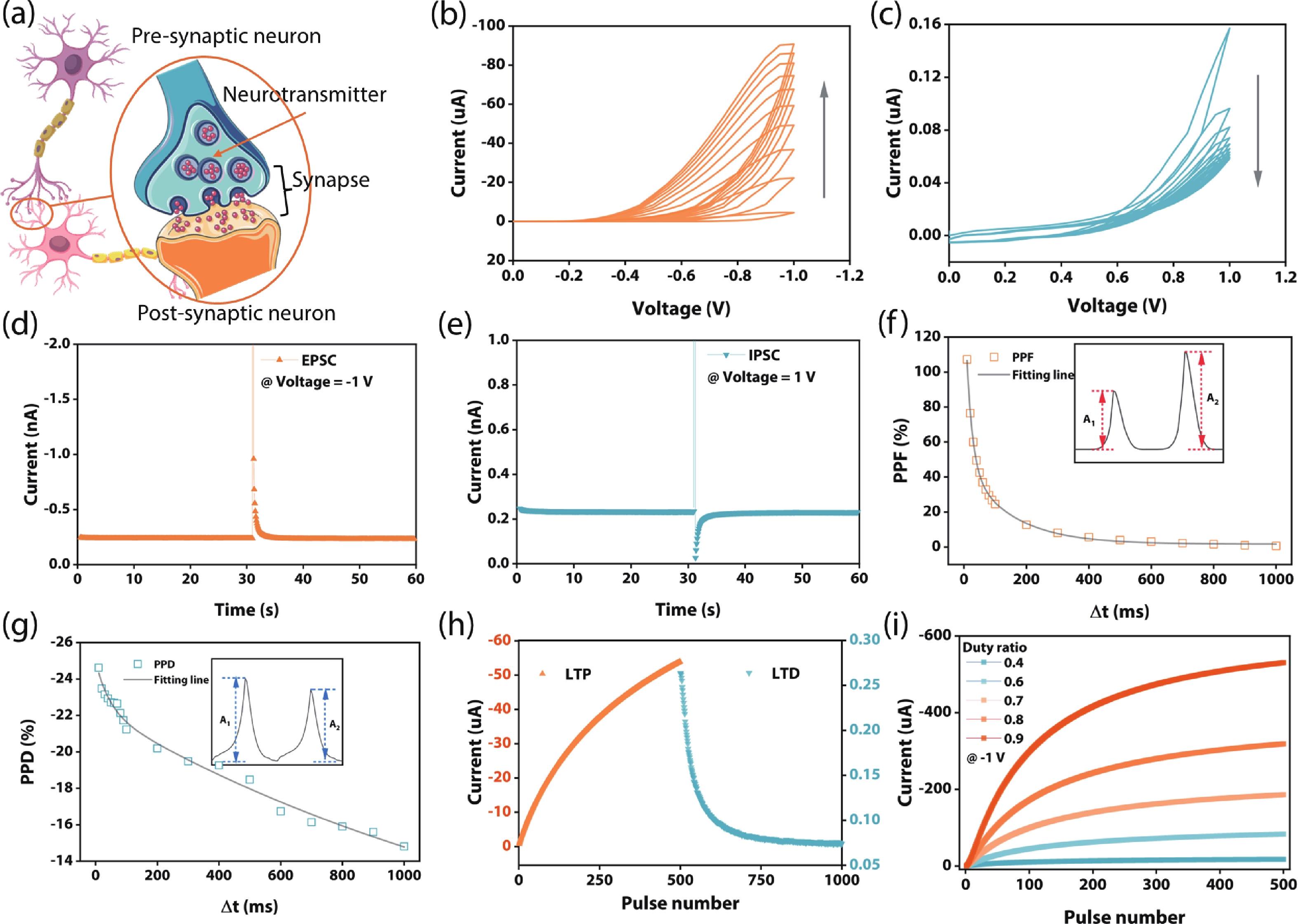
In the human brain, synapses are the foundation unit for bearing the responsibility of connecting neurons and transmitting nerve impulses[33]. They can be divided into three parts, including pre-synaptic neuron, synaptic cleft, and post-synaptic neuron, where the neurotransmitters in pre-synaptic neuron act as the carrier for nerve impulse transmission to post-synaptic neuron, as shown in Fig. 2(a). And the exciting potential in post-synaptic neuron follows a gradual change trend, which can be mimicked by the presented synaptic device, as shown in Figs. 2(b) and 2(c). Ten cycles of negative sweeping voltage (0→–1 V→0) and positive sweeping voltage (0→1 V→0) are used to continuously stimuli the top electrode. Increasing and decreasing trends illustrate the voltage with different polarity carries a diametrically opposed excited effect, which is similar to the disparate influences of the cations (Ca2+) and anions (Cl1−) for post-synaptic membrane[34]. This phenomenon is also validated by the vivid trends in further current sequence diagrams in Figs. S3(a) and S3(b) (Supplementary Material). To probe the response sensitivity of the electrical synapse, the excitatory post-synaptic current (EPSC) and inhibitory post-synaptic current (IPSC) are measured by a single pulse (duration: 50 ms, interval: 50 ms, reading voltage: –0.1 V and 0.1 V) with the amplitudes of –1 and 1 V, respectively. It can be seen that the currents rise and fall suddenly and then return to initial values gradually, as depicted in Figs. 2(d) and 2(e). When the pulse executes two consecutive actions, PPF and PPD with the effective outputs of current can be observed, as the insets shown in Figs. 2(f) and 2(g). Following the formula:

Fig. 2.  (Color online) (a) Schematic illustration of the neural signal transmission by biological synapses. The continuous 10 sweeping curves at (b) negative voltage (0→–1 V→0) and (c) positive voltage (0→1 V→0). The (d) EPSC and (e) IPSC at (excitation/inhibition) pulse of –1 and 1 V, respectively. The (f) PPF and (g) PPD as well as their fitting lines at negative and positive paired electrical pulses, respectively. (h) The LTP and LTD induced by 1000 negative and positive electrical pulses. (i) The LTP induced by negative electrical pulses with different duty ratios (0.4, 0.6, 0.7, 0.8, and 0.9).
PPF/PPD(%)=A2A1A1×100%.
(1)

The PPF/PPD indexes are defined as the ratio of current induced by the second pulse (A2) to the first (A1). The relationships between PPF/PPD (%) and interval are drawn and fitted in Figs. 2(f) and 2(g). The fitting function is given as:

PPF/PPDindex=c1exp(tτ1)+c2exp(tτ2),
(2)

where t is the interval time, c1 and c2 are the initial facilitation magnitudes of the respective phases, τ1 and τ2 are the characteristic relaxation time constant). Both exponential declines illustrate the paired pulses will turn into ineffective with the interval increasing. The characteristic relaxation time constants τ1 and τ2 are 18.57 and 149.29 ms (PPF) as well as 45.02 and 1583.51 ms (PPD), which is consistent with the biological value[17, 33, 35]. Expanding the number of pulses to 500, significant effective current outputs, i.e., long-term potentiation and depression (LTP/LTD) are obtained, shown in Fig. 2(h). And such robust inter-synaptic connectivity is also harmonized by changing the duty ratio of pulses, as shown in Fig. 2(i), the rising duty ratio can induce the amplitude and speed of the effective current outputs to grow to a great extent. After the expanded pulses stimulating, the electrical synapse transits to a relaxation state, which means the grown currents enter to decay naturally. As depicted in Fig. S3(c) (Supplementary Material), the relaxation rate slows down with the duty ratio decreasing. The above results demonstrate the excellent performance of the electrical synapse, and the synaptic device lays an enormous potential for future brain-like computing.

To analyze the current–voltage characteristics, the I–V sweeping curves of MFOS are measured, as depicted in Fig. S4 (Supplementary Material). There are less or no conspicuous performances of memorizing resistance in Al/Ga2O3(OR)/ITO and Al/Ga2O3(OD)/ITO, as shown in Figs. S4(a) and S4(b). While the MFOS exhibits both hysteresis processes between rounds 1 and 2 as well as rounds 3 and 4, as depicted in Figs. S4(c) and S4(d). In addition, the rectification phenomenon can be observed apparently, which indicates that there is a Schottky potential barrier between the two Ga2O3 films[18, 31, 32]. Continuous positive sweeping high resistance state (HRS) are fitted by Schottky Emission (SE) model in Fig. S5. Fitted straight line with excellent linearity gradually shifts upwards with the cycles, which is consistent with the gradual increase in current under the positive voltages presented in Fig. 2(b). They can be attributed to the transport and trapped/de-trapped of oxygen vacancies and electronics at the interface, as shown in Fig. S6. And the slow decay process in Fig. S3(c) is induced by oxygen ions back-diffusion owing to the existing of oxygen concentration gradient, which lay the foundation for non-volatile memories of the electrical synapse[31, 36].

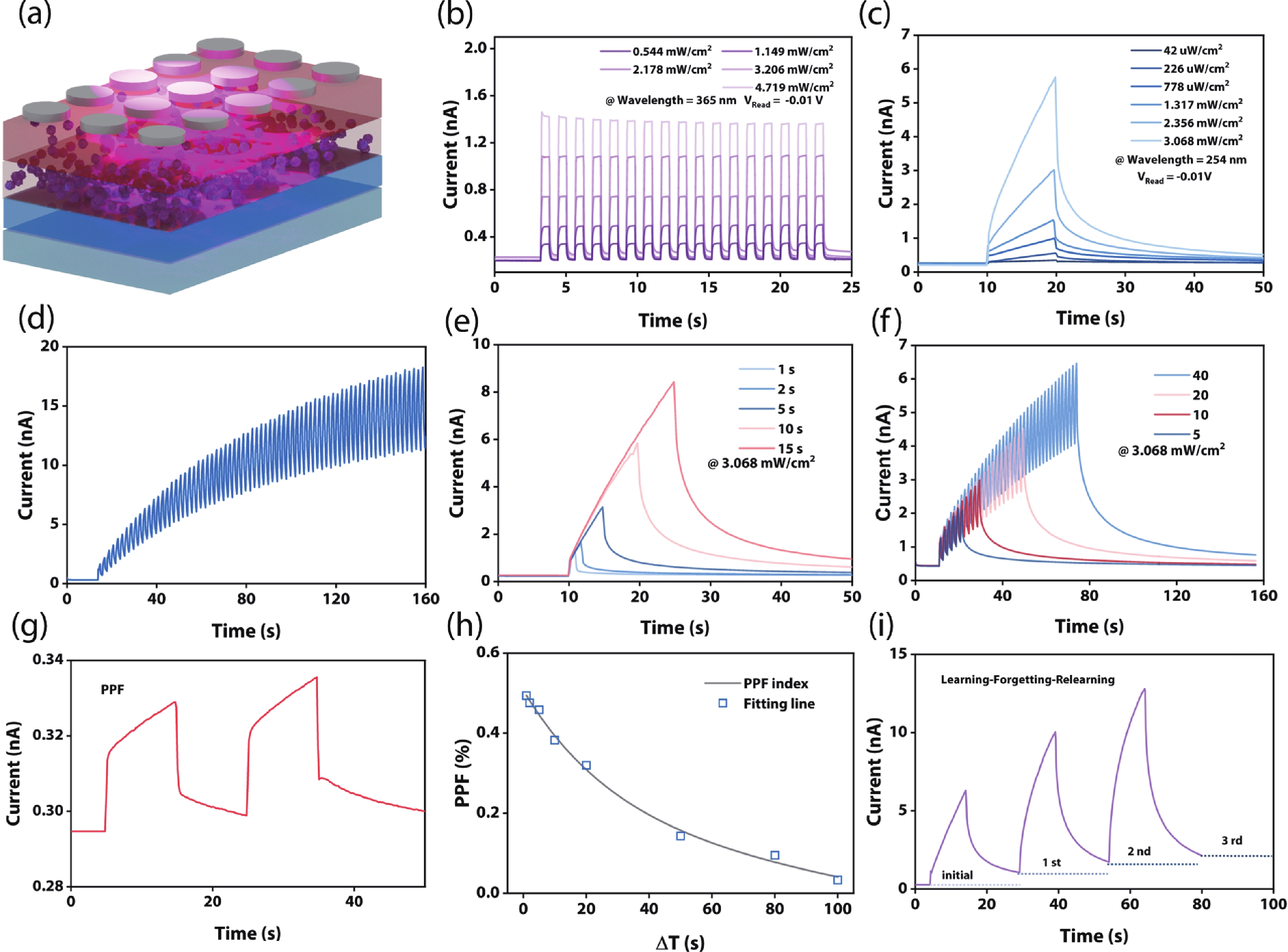
Not only that, but the defect capture and energy band transport are also the principal mechanisms of optical synaptic behaviors with the participation of photoconductive effect. As the MFOS is illuminated by the light like in Fig. 3(a), photons energy will be absorbed and the electronics bound in the valence band can be excited, resulting in the transition to the conduction band and the formation of the photocurrent. Comparing the values and trend of the increasing photocurrent in Figs. 3(b) and 3(c), it can be found that the transitioned electronics evoked by the light at the wavelength of 254 nm are greater in number than that of 365 nm and the synaptic behavior disappears under the illumination of 365 nm. As demonstrated by the absorption spectrum shown in Fig. S7(a) (Supplementary Material), the 365 nm light causes almost no photocarriers generation in Ga2O3(OR), it does not trigger the photocarriers trapped/de-trapped process, thereby resulting in no synaptic behavior[11, 13]. While massive photocarriers in Ga2O3(OR) and Ga2O3(OD) can be excited by 254 nm light, leading to the potential barriers change (Fig. S8(b)), and once withdraw the light, the photocarriers will recombine or be trapped (Fig. S8(c)). In addition, as the bottom electrode, ITO has the ability to absorb UV light, as illustrated in Fig. S7(b). Comparing the ITO device with the n-Si device in Figs. S7(c) and S7(d), it can be seen that the optical synaptic tendency of the device does not depend on the bottom electrode. We speculate that the ITO serves to improve the optical response for the homojunction devices. And the optical synaptic behaviors with specific light are demonstrated as follows.

Fig. 3.  (Color online) (a) The schematic diagram of the device under light. The photocurrent responses of the device under different lights of (b) 365 nm and (c) 254 nm with varying intensity. (d) The photocurrent response under consecutive optical pulses (3.068 mW/cm2: 1 s, dark: 1 s). The photocurrent responses of the device under 254 nm light with different (e) durations (1, 2, 5, 10, and 15 s) and (f) pulse numbers (5, 10, 20, and 40). (g) The PPF induced by paired optical pulses. (h) The variation of the PPF index with the intervals of paired optical pulses. (i) The “Learning-Forgetting-Relearning” process induced by three periodic lights (3.068 mW/cm2: 10 s and dark: 15 s).

With the gradually rising photocurrent response under consecutive optical pulses, the memory characterization of the synaptic device can be revealed in Fig. 3(d). In biological systems, the sensory cells respond differently to the input signal with diverse variables[20, 25]. Similarly, the regularly changing photocurrents will be induced by the light with varying parameters of duration and pulse number, as shown in Figs. 3(e) and 3(f), respectively. The prolonged duration (1, 2, 5, 10, 15 s) acts as a boost to the response of the device, and also maintains the relaxing current for a long time (>30 s) after turning off the light. As for the pulse number, the same increasing and relaxing trend of current occurs as the number of pulses varies (5, 10, 20, 40) and the time consumed (from <35 s to >80 s) by the relaxation process which indicates the short-term memory (STM) is transmitted to long-term memory (LTM). In addition, critical synaptic plasticity called PPF is a short-term potentiation process essential to decoding temporal information in optical signals. As shown in Fig. 3(g), the optical pulse pairs are employed to enhance memory strength. And the relationship between the PPF index and optical pulse interval is depicted in Fig. 3(h) which is consistent with the electrical PPF behavior, while the fitted characteristic relaxation time constants of τ1 (29.45 s) and τ2 (1.99 × 10⁶ s) are larger than that of electrical PPF, which results from the slower recombination of light-induced electrons and holes than the back-diffusion effect of the oxygen vacancies. On this bias, the advanced synaptic function of “Learning-Forgetting-Relearning” is further simulated as testified in Fig. 3(i), the photocurrent induced by first and following twice reillumination increases, in turn, leading to the effective prolongation of relaxation process. In brief, the responses of the device dominated by optical signals and its ability of repetitive learning and forgetting demonstrate the optical synapse integrating both functions of perception and memory is realized.

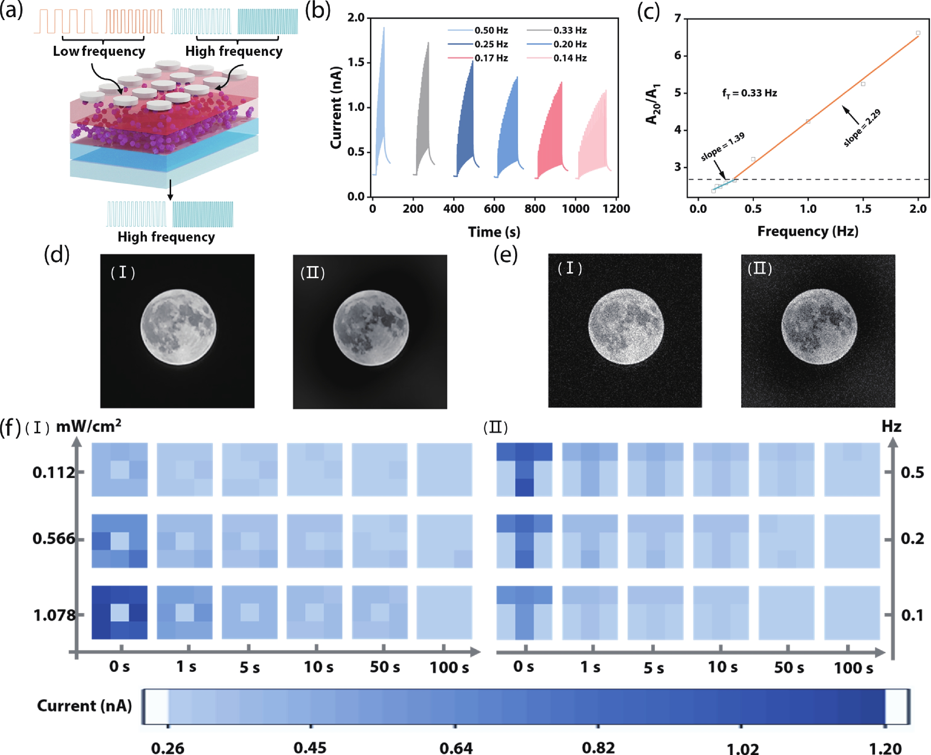
In the visual synaptic unit, the low-probability release of neurotransmitters possesses a high-pass filtering action[19, 37, 38]. The high-pass filter provides a self-scoring line for the signal frequency and outputs high-frequency signals above this threshold while low-frequency signals are filtered out. The MFOS possesses the capability of mimicking such a high-pass filter and the diagram of the device’s filtering effect is depicted in Fig. 4(a). To measure the filtering behavior of the optical synapse, 20 optical pulses with varying frequencies (2, 1.5, 1, 0.5, 0.33, 0.25, 0.20, 0.17, and 0.14 Hz) are imposed, as shown in Fig. 4(b) and Fig. S9. It can be seen that the increasing induces a higher current response, and Fig. 4(c) summarizes the dependence of EPSC (defined as the current value ratio by the 20th and 1st pulse, i.e. A20/A1) on the pulse frequency. The EPSC points can be separately fitted into two types of the straight line with discrepant slopes (1.39 and 2.29). Filtering out the part with a lower slope and extracting the turning point (0.33 Hz) as threshold frequency (fT), the design of the high-pass filter is completed. To testify its filtering performance, the optical synapse is used to filter the original moon images, and the original data and outcomes are exhibited in Fig. 4(d). However, imaging is subject to hardware noise, such as Gaussian noise resulting from low illumination levels, high temperatures, and low temperatures. Not only that, but imaging sensor suffers from sudden and strong disturbances, including incorrect switching operations and failed light sensors, which may produce unavoidable Salt-and-Pepper noise. Therefore, it is necessary to apply high-pass filter to noise-doped image processing, as shown in Fig. 4(e) and Fig. S10. It is observed that whether Gaussian or Salt-and-Pepper noise, the filter extracts the feature frequency of the image, and the sharpened images are displayed. As a consequence, the high-pass filtering optical synapse is realized.

Fig. 4.  (Color online) The high-pass filter and visual system. (a) The diagram of MFOS’s filtering effect. (b) The photocurrent responses triggered by 20 optical pulses with declining pulse frequencies (0.5, 0.33, 0.25, 0.20, 0.17, and 0.14 Hz). (c) Dependence of the EPSC (A20/A1) on the pulse frequency. The threshold frequency (fT) is 0.33 Hz. (d) The filtering process of the image moon. (Ⅰ) The original image. (Ⅱ) The high-pass filtered image. (e) The filtering process of the moon image with Gaussian noise. (Ⅰ) The original image with Gaussian noise. (Ⅱ) The high-pass filtered image. (f) The perception and memory characteristics of the MFOS-based visual system under illumination with varying (Ⅰ) intensity and (Ⅱ) frequency.

Beyond filtering functions, optical synapse holds great potential for bionic applications due to its integrated functions of perception and memory. In the human visual system, the cone and rod cells distributed in retina are responsible for receiving and recognizing external optical information, and its transfer to visual cortex is then achieved by optic nerve[9, 17]. Herein, the series of processes can be fulfilled on the single prepared optical synapses. As shown in Fig. 4(f), a 3 × 3 MFOS array is constructed to mimic the retina, where the letters “O” and “T” hollowed on the mask reticle represent the image on retina and the color saturation corresponds to the photocurrent response of the MFOS unit as well as the memory strength of acquired visual information. Adjusting two illumination parameters of intensity (Figs. 4(f)-Ⅰ) and frequency (Fig. 4(f)-Ⅱ), it can be observed that when enhancing the intensity (from 0.112 to 1.078 mW/cm2), the memory strength for the letter “O” is strengthened from ~0.45 to ~1.2 nA, while forgetting time lengthens from 1 s to >50 s. Similarly, with the hastening of frequency (from 0.1 to 0.5 Hz), the memory strength for the letter “T” is also strengthened from ~0.64 to ~1.2 nA, and forgetting time lengthens from 10 to >50 s. Therefore, the filtering effect on small signals can be demonstrated and the optically regulable perception-memory integrated artificial visual system is realized.

In the human brain nervous system, associative learning behavior is an advanced learning function which requires multiple signals to work together. Pavlovian conditioning reflex experience, one of the most classic examples, is testified successfully by measuring the puppy’s responsiveness with the co-modulation of ringing and feeding signals, which is interpreted in Fig. 5(a)[27, 39, 40]. As previously described and exhibited in Figs. 3(b) and 3(c), the MFOS is able to respond to double irradiated wavelengths of 254 and 365 nm. And the nonvolatile characteristic under the wavelength of 254 nm in collaboration with the volatile characteristic under the wavelength of 365 nm paves the way for simulating the Pavlovian conditioning reflex experience. As shown in Figs. 5(b)-Ⅰ and 5(b)-Ⅱ, the optical signal of 365 nm (976 μW/cm2) which acts as the ringing bell for puppy is initially applied to the device. And the optical signal of 254 nm (976 μW/cm2) which acts as feeding food for puppy is then applied. Different photocurrent responses which mean failed firing (<0.6 nA) and firing (>0.6 nA) respectively can be found from Figs. 5(c)-Ⅰ and 5(c)-Ⅱ. It indicates that the artificial “puppy” performs well to the external stimuli. Immediately after, once the double optical signals of 365 nm (ringing bell) and 254 nm (feeding food) irradiate the artificial “puppy” in parallel (Fig. 5(b)-Ⅲ)), the firing state is awakened to a high level instantly (Fig. 5(c)-Ⅲ)). Silence for a while and the artificial “puppy” fires again that followed by applying the optical signals of 365 nm (Fig. 5(b)-Ⅳ). Thus, the associative learning behavior of Pavlovian conditioning reflex experience is completed by the MFOS under the participation with two optical signals of 365 and 254 nm.

Fig. 5.  (Color online) The implementation of Pavlovian associative learning. (a) The four conversion processes of the puppy when (Ⅰ) only the bell rings, (Ⅱ) only feeding, (Ⅲ) bell ringing and feeding occur in parallel, and (Ⅳ) bell rings again. (b) The four kinds of optical signal arrangements and combinations (wavelength: 365 and 254 nm, intensity: 976 μW/cm2). (Ⅰ) only 365 nm, (Ⅱ) only 254 nm, (Ⅲ) 365 nm and 254 nm in parallel, and (Ⅳ) only 365 nm again. (c) The state conversion of the device from (Ⅰ) failed firing to (Ⅱ–Ⅳ) firing (threshold current is 0.6 nA).

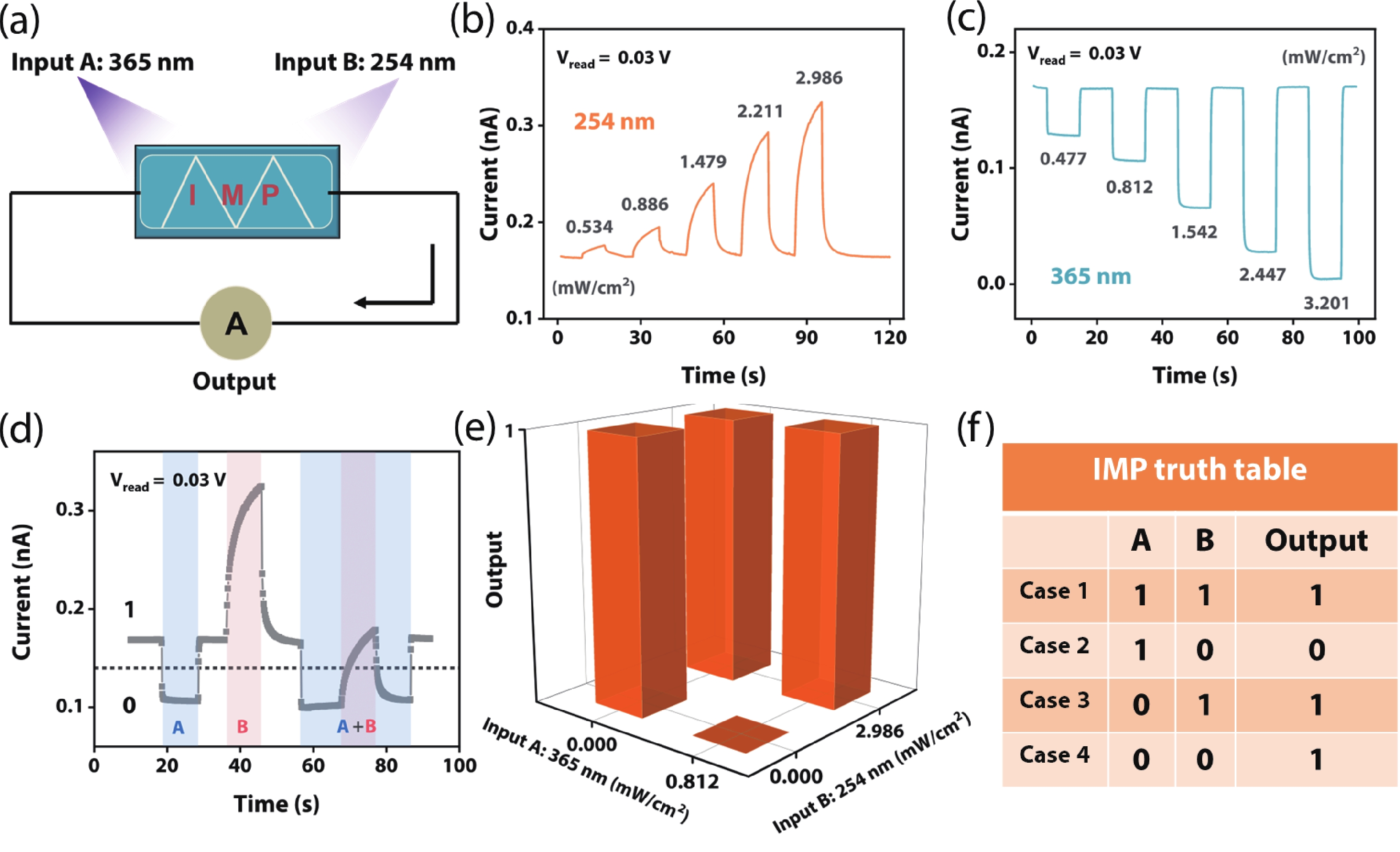
In addition, the distinctive photocurrent responses of the MFOS are presented under the different reading voltage (Vread) of 0.03 V to implement the logic gate of IMP. As shown in Figs. 6(a) and 6(b), the relaxation processes induced by the optical signal of 254 nm at the Vread of 0.03 V are shorter than that at the Vread of –0.01 V and the current value of MFOS is inhibited under the irradiation of the optical signal of 365 nm, which can be attributed to the diametrically opposite influence of the potential barrier between the homojunction on the reversed electric field direction[36, 41]. Taking advantage of such characteristics and selecting appropriate illumination intensity of 2.986 mW/cm2 for 254 nm and 0.812 mW/cm2 for 365 nm as the inputs. By arranging and combining the turning on and off of the two illuminating signals, the different photocurrents of the device are output, and a threshold value of 0.14 nA is present to distinguish the logic “0” and “1”, as shown in Fig. 6(c). Summering the measured results, the logic relationship between optical inputs and current output is depicted in Fig. 6(d) and the situ logic gate of IMP is implemented with the truth table indicated in Fig. 6(e). The results pave the way for in-sensor and parallel computation in neural morphology devices.

Fig. 6.  (Color online) (a) The diagram of the IMP logic gate. Different responses for the optical signals of (b) 254 nm and (c) 365 nm with varying intensity at a Vread of 0.03 V. The (d) measured data, (e) logic data, and (f) truth table of the logic gate of IMP (threshold current is 0.14 nA).

In this work, the MFOS based on the Ga2O3(OD)/Ga2O3(OR) homojunction is prepared and demonstrated. The basic synaptic functions such as PPF/PPD and LTP/LTD are realized due to the carrier trapping/de-trapping and energy band differences between homojunction in response to the stimulation of electrical signals. In addition, the optical signals also exhibit the ability to induce synaptic behaviors in the same device. Based on the photoconductive effect and the sensitivity of MFOS to optical frequency, the high-pass filtering property is verified. Meanwhile, the visual system with perception-memory integrated capability is implemented by changing the light signal with the parameters of intensity and frequency. Furthermore, the classic experience of the Pavlovian conditioning reflex and the logic gate of IMP are demonstrated under co-modulation with dual-band wavelength illumination. In brief, this work proposes a strategy to construct MFOS with the engagement of multiple signals, thus further providing an effective platform for future multi-scenario applications of neuromorphic computing.

This work was supported by the National Natural Science Foundation of China under Grant (62174068, 61625404).

Supplementary materials to this article can be found online at https://doi.org/10.1088/1674-4926/44/7/074101.


[1]
Wang Y H, Yang Y C, Hao Y, et al. Embracing the era of neuromorphic computing. J Semicond, 2021, 42, 010301 doi: 10.1088/1674-4926/42/1/010301
[2]
Mpatziakas A, Drosou A, Papadopoulos S, et al. IoT threat mitigation engine empowered by artificial intelligence multi-objective optimization. J Netw Comput Appl, 2022, 203, 103398 doi: 10.1016/j.jnca.2022.103398
[3]
Yao T C, Wang J, Wan M, et al. VenusAI: an artificial intelligence platform for scientific discovery on supercomputers. J Syst Architect, 2022, 128, 102550 doi: 10.1016/j.sysarc.2022.102550
[4]
Sokolov A S, Abbas H, Abbas Y, et al. Towards engineering in memristors for emerging memory and neuromorphic computing: A review. J Semicond, 2021, 42, 013101 doi: 10.1088/1674-4926/42/1/013101
[5]
Zou X Q, Xu S, Chen X M, et al. Breaking the von Neumann bottleneck: architecture-level processing-in-memory technology. Sci China Inf Sci, 2021, 64, 160404 doi: 10.1007/s11432-020-3227-1
[6]
Sandamirskaya Y, Kaboli M, Conradt J, et al. Neuromorphic computing hardware and neural architectures for robotics. Sci Robot, 2022, 7, eabl8419 doi: 10.1126/scirobotics.abl8419
[7]
Xue W H, Ci W J, Xu X H, et al. Optoelectronic memristor for neuromorphic computing. Chin Phys B, 2020, 29, 048401 doi: 10.1088/1674-1056/ab75da
[8]
Xiang S Y, Han Y N, Song Z W, et al. A review: Photonics devices, architectures, and algorithms for optical neural computing. J Semicond, 2021, 42, 023105 doi: 10.1088/1674-4926/42/2/023105
[9]
Han J, Yun S, Lee S, et al. A review of artificial spiking neuron devices for neural processing and sensing. Adv Funct Mater, 2022, 32, 2204102 doi: 10.1002/adfm.202204102
[10]
Zhou F C, Zhou Z, Chen J W, et al. Optoelectronic resistive random access memory for neuromorphic vision sensors. Nat Nanotechnol, 2019, 14, 776 doi: 10.1038/s41565-019-0501-3
[11]
Liao F Y, Zhou F C, Chai Y. Neuromorphic vision sensors: principle, progress and perspectives. J Semicond, 2021, 42, 013105 doi: 10.1088/1674-4926/42/1/013105
[12]
Shastri B J, Tait A N, Ferreira de Lima T, et al. Photonics for artificial intelligence and neuromorphic computing. Nat Photonics, 2021, 15, 102 doi: 10.1038/s41566-020-00754-y
[13]
Liu Q, Gao S, Xu L, et al. Nanostructured perovskites for nonvolatile memory devices. Chem Soc Rev, 2022, 51, 9 doi: 10.1039/D1CS00886B
[14]
Chen S, Lou Z, Chen D, et al. An artificial flexible visual memory system based on an UV-motivated memristor. Adv Mater, 2018, 30, 1705400 doi: 10.1002/adma.201705400
[15]
Tsai M Y, Lee K C, Lin C Y, et al. Photoactive electro-controlled visual perception memory for emulating synaptic metaplasticity and Hebbian learning. Adv Funct Mater, 2021, 31, 2105345 doi: 10.1002/adfm.202105345
[16]
Du W, Li C H, Hu Y X, et al. A heterosynapse-inspired photodetector for spatiotemporal feature fusion. IEEE Trans Electron Devices, 2022, 69, 4312 doi: 10.1109/TED.2022.3179347
[17]
Gong J D, Wei H H, Liu J Q, et al. An artificial visual nerve for mimicking pupil reflex. Matter, 2022, 5, 1578 doi: 10.1016/j.matt.2022.02.020
[18]
Feng G D, Jiang J, Li Y R, et al. Flexible vertical photogating transistor network with an ultrashort channel for in-sensor visual nociceptor. Adv Funct Mater, 2021, 31, 2104327 doi: 10.1002/adfm.202104327
[19]
Ding G L, Yang B D, Zhou K, et al. Synaptic plasticity and filtering emulated in metal-organic frameworks nanosheets based transistors. Adv Electron Mater, 2020, 6, 1900978 doi: 10.1002/aelm.201900978
[20]
Elliott T. First passage time memory lifetimes for multistate, filter-based synapses. Neural Comput, 2020, 32, 1069 doi: 10.1162/neco_a_01283
[21]
Dai Y T, Fu Y M, Zeng H, et al. A self-powered brain-linked vision electronic-skin based on triboelectric-photodetecing pixel-addressable matrix for visual-image recognition and behavior intervention. Adv Funct Mater, 2018, 28, 1800275 doi: 10.1002/adfm.201800275
[22]
Huang B Y, Li N, Wang Q Q, et al. Optoelectronic synapses based on MoS2 transistors for accurate image recognition. Adv Mater Interfaces, 2022, 2201558 doi: 10.1002/admi.202201558
[23]
Xie D D, Yin K, Yang Z J, et al. Polarization-perceptual anisotropic two-dimensional ReS2 neuro-transistor with reconfigurable neuromorphic vision. Mater Horiz, 2022, 9, 1448 doi: 10.1039/D1MH02036F
[24]
Zhang Z H, Wang S Y, Liu C S, et al. All-in-one two-dimensional retinomorphic hardware device for motion detection and recognition. Nat Nanotechnol, 2022, 17, 27 doi: 10.1038/s41565-021-01003-1
[25]
Jiang B Y, Zhou F C, Chai Y. Application of neuromorphic resistive random access memory in image processing. Acta Phys Sin, 2022, 71, 148504 doi: 10.7498/aps.71.20220463
[26]
Liu Q H, Yin L, Zhao C, et al. All-in-one metal-oxide heterojunction artificial synapses for visual sensory and neuromorphic computing systems. Nano Energy, 2022, 97, 107171 doi: 10.1016/j.nanoen.2022.107171
[27]
Zhang J Y, Shi Q Q, Wang R Z, et al. Spectrum-dependent photonic synapses based on 2D imine polymers for power-efficient neuromorphic computing. InfoMat, 2021, 3, 904 doi: 10.1002/inf2.12198
[28]
Wang Y H, Cui W J, Yu J, et al. One-step growth of amorphous/crystalline Ga2O3 phase junctions for high-performance solar-blind photodetection. ACS Appl Mater Interfaces, 2019, 11, 45922 doi: 10.1021/acsami.9b17409
[29]
Huang J, Chang T, Yang J, et al. Influence of oxygen concentration on resistance switching characteristics of gallium oxide. IEEE Electron Device Lett, 2012, 33, 1387 doi: 10.1109/LED.2012.2206365
[30]
Bhowmick S, Saha R, Mishra M, et al. Oxygen mediated defect evolution in RF sputtered Ga2O3 thin films on p-Si substrate. Mater Today Commun, 2022, 104766 doi: 10.1016/j.mtcomm.2022.104766
[31]
Hu L X, Yang J, Wang J R, et al. All-optically controlled memristor for optoelectronic neuromorphic computing. Adv Funct Mater, 2021, 31, 2005582 doi: 10.1002/adfm.202005582
[32]
Karbalaei Akbari M, Hu J, Verpoort F, et al. Nanoscale all-oxide-heterostructured bio-inspired optoresponsive nociceptor. Nano-Micro Lett, 2020, 12, 83 doi: 10.1007/s40820-020-00419-z
[33]
Wu F Q, Guo Y T, Ma J. Reproduce the biophysical function of chemical synapse by using a memristive synapse. Nonlinear Dyn, 2022, 109, 2063 doi: 10.1007/s11071-022-07533-0
[34]
Held R, Liu C L, Ma K P, et al. Synapse and active zone assembly in the absence of presynaptic Ca2+ channels and Ca2+ entry. Neuron, 2020, 107, 667 doi: 10.1016/j.neuron.2020.05.032
[35]
Kim M, Lee J. Synergistic improvement of long-term plasticity in photonic synapses using ferroelectric polarization in hafnia-based oxide-semiconductor transistors. Adv Mater, 2020, 32, 1907826 doi: 10.1002/adma.201907826
[36]
Wang W X, Gao S, Li Y, et al. Artificial optoelectronic synapses based on TiNxO2–x/MoS2 heterojunction for neuromorphic computing and visual system. Adv Funct Mater, 2021, 31, 2101201 doi: 10.1002/adfm.202101201
[37]
Thomson A. Molecular frequency filters at central synapses. Prog Neurobiol, 2000, 62, 159 doi: 10.1016/S0301-0082(00)00008-3
[38]
Suh B, Baccus S. Building blocks of temporal filters in retinal synapses. PLoS Biol, 2014, 12, e1001973 doi: 10.1371/journal.pbio.1001973
[39]
Tan Z H, Yin X B, Yang R, et al. Pavlovian conditioning demonstrated with neuromorphic memristive devices. Sci Rep, 2017, 7, 713 doi: 10.1038/s41598-017-00849-7
[40]
Li J, Fu W H, Lei Y X, et al. Oxygen-vacancy-induced synaptic plasticity in an electrospun InGdO nanofiber transistor for a gas sensory system with a learning function. ACS Appl Mater Interfaces, 2022, 14, 8587 doi: 10.1021/acsami.1c23390
[41]
Shi J J, Lin Y, Zeng T, et al. Voltage-dependent plasticity and image Boolean operations realized in a WOx-based memristive synapse. J Semicond, 2021, 42, 014102 doi: 10.1088/1674-4926/42/1/014102
Fig. 1.  (Color online) (a) The schematic diagram and (b) the cross-sectional SEM image of the device. The XRD spectra of (c) Ga2O3(OD) and (d) Ga2O3(OR). The XPS spectra of (e, f) Ga 2p3/2 peak, as well as (g, h) O 1s peak in two different oxygen-content films. (i) The valence band XPS spectra and (j) UPS spectra of Ga2O3(OD) and Ga2O3(OR). (k) The energy band diagrams and (l) schematic of carrier distribution of Ga2O3(OD) and Ga2O3(OR).

Fig. 2.  (Color online) (a) Schematic illustration of the neural signal transmission by biological synapses. The continuous 10 sweeping curves at (b) negative voltage (0→–1 V→0) and (c) positive voltage (0→1 V→0). The (d) EPSC and (e) IPSC at (excitation/inhibition) pulse of –1 and 1 V, respectively. The (f) PPF and (g) PPD as well as their fitting lines at negative and positive paired electrical pulses, respectively. (h) The LTP and LTD induced by 1000 negative and positive electrical pulses. (i) The LTP induced by negative electrical pulses with different duty ratios (0.4, 0.6, 0.7, 0.8, and 0.9).

Fig. 3.  (Color online) (a) The schematic diagram of the device under light. The photocurrent responses of the device under different lights of (b) 365 nm and (c) 254 nm with varying intensity. (d) The photocurrent response under consecutive optical pulses (3.068 mW/cm2: 1 s, dark: 1 s). The photocurrent responses of the device under 254 nm light with different (e) durations (1, 2, 5, 10, and 15 s) and (f) pulse numbers (5, 10, 20, and 40). (g) The PPF induced by paired optical pulses. (h) The variation of the PPF index with the intervals of paired optical pulses. (i) The “Learning-Forgetting-Relearning” process induced by three periodic lights (3.068 mW/cm2: 10 s and dark: 15 s).

Fig. 4.  (Color online) The high-pass filter and visual system. (a) The diagram of MFOS’s filtering effect. (b) The photocurrent responses triggered by 20 optical pulses with declining pulse frequencies (0.5, 0.33, 0.25, 0.20, 0.17, and 0.14 Hz). (c) Dependence of the EPSC (A20/A1) on the pulse frequency. The threshold frequency (fT) is 0.33 Hz. (d) The filtering process of the image moon. (Ⅰ) The original image. (Ⅱ) The high-pass filtered image. (e) The filtering process of the moon image with Gaussian noise. (Ⅰ) The original image with Gaussian noise. (Ⅱ) The high-pass filtered image. (f) The perception and memory characteristics of the MFOS-based visual system under illumination with varying (Ⅰ) intensity and (Ⅱ) frequency.

Fig. 5.  (Color online) The implementation of Pavlovian associative learning. (a) The four conversion processes of the puppy when (Ⅰ) only the bell rings, (Ⅱ) only feeding, (Ⅲ) bell ringing and feeding occur in parallel, and (Ⅳ) bell rings again. (b) The four kinds of optical signal arrangements and combinations (wavelength: 365 and 254 nm, intensity: 976 μW/cm2). (Ⅰ) only 365 nm, (Ⅱ) only 254 nm, (Ⅲ) 365 nm and 254 nm in parallel, and (Ⅳ) only 365 nm again. (c) The state conversion of the device from (Ⅰ) failed firing to (Ⅱ–Ⅳ) firing (threshold current is 0.6 nA).

Fig. 6.  (Color online) (a) The diagram of the IMP logic gate. Different responses for the optical signals of (b) 254 nm and (c) 365 nm with varying intensity at a Vread of 0.03 V. The (d) measured data, (e) logic data, and (f) truth table of the logic gate of IMP (threshold current is 0.14 nA).

[1]
Wang Y H, Yang Y C, Hao Y, et al. Embracing the era of neuromorphic computing. J Semicond, 2021, 42, 010301 doi: 10.1088/1674-4926/42/1/010301
[2]
Mpatziakas A, Drosou A, Papadopoulos S, et al. IoT threat mitigation engine empowered by artificial intelligence multi-objective optimization. J Netw Comput Appl, 2022, 203, 103398 doi: 10.1016/j.jnca.2022.103398
[3]
Yao T C, Wang J, Wan M, et al. VenusAI: an artificial intelligence platform for scientific discovery on supercomputers. J Syst Architect, 2022, 128, 102550 doi: 10.1016/j.sysarc.2022.102550
[4]
Sokolov A S, Abbas H, Abbas Y, et al. Towards engineering in memristors for emerging memory and neuromorphic computing: A review. J Semicond, 2021, 42, 013101 doi: 10.1088/1674-4926/42/1/013101
[5]
Zou X Q, Xu S, Chen X M, et al. Breaking the von Neumann bottleneck: architecture-level processing-in-memory technology. Sci China Inf Sci, 2021, 64, 160404 doi: 10.1007/s11432-020-3227-1
[6]
Sandamirskaya Y, Kaboli M, Conradt J, et al. Neuromorphic computing hardware and neural architectures for robotics. Sci Robot, 2022, 7, eabl8419 doi: 10.1126/scirobotics.abl8419
[7]
Xue W H, Ci W J, Xu X H, et al. Optoelectronic memristor for neuromorphic computing. Chin Phys B, 2020, 29, 048401 doi: 10.1088/1674-1056/ab75da
[8]
Xiang S Y, Han Y N, Song Z W, et al. A review: Photonics devices, architectures, and algorithms for optical neural computing. J Semicond, 2021, 42, 023105 doi: 10.1088/1674-4926/42/2/023105
[9]
Han J, Yun S, Lee S, et al. A review of artificial spiking neuron devices for neural processing and sensing. Adv Funct Mater, 2022, 32, 2204102 doi: 10.1002/adfm.202204102
[10]
Zhou F C, Zhou Z, Chen J W, et al. Optoelectronic resistive random access memory for neuromorphic vision sensors. Nat Nanotechnol, 2019, 14, 776 doi: 10.1038/s41565-019-0501-3
[11]
Liao F Y, Zhou F C, Chai Y. Neuromorphic vision sensors: principle, progress and perspectives. J Semicond, 2021, 42, 013105 doi: 10.1088/1674-4926/42/1/013105
[12]
Shastri B J, Tait A N, Ferreira de Lima T, et al. Photonics for artificial intelligence and neuromorphic computing. Nat Photonics, 2021, 15, 102 doi: 10.1038/s41566-020-00754-y
[13]
Liu Q, Gao S, Xu L, et al. Nanostructured perovskites for nonvolatile memory devices. Chem Soc Rev, 2022, 51, 9 doi: 10.1039/D1CS00886B
[14]
Chen S, Lou Z, Chen D, et al. An artificial flexible visual memory system based on an UV-motivated memristor. Adv Mater, 2018, 30, 1705400 doi: 10.1002/adma.201705400
[15]
Tsai M Y, Lee K C, Lin C Y, et al. Photoactive electro-controlled visual perception memory for emulating synaptic metaplasticity and Hebbian learning. Adv Funct Mater, 2021, 31, 2105345 doi: 10.1002/adfm.202105345
[16]
Du W, Li C H, Hu Y X, et al. A heterosynapse-inspired photodetector for spatiotemporal feature fusion. IEEE Trans Electron Devices, 2022, 69, 4312 doi: 10.1109/TED.2022.3179347
[17]
Gong J D, Wei H H, Liu J Q, et al. An artificial visual nerve for mimicking pupil reflex. Matter, 2022, 5, 1578 doi: 10.1016/j.matt.2022.02.020
[18]
Feng G D, Jiang J, Li Y R, et al. Flexible vertical photogating transistor network with an ultrashort channel for in-sensor visual nociceptor. Adv Funct Mater, 2021, 31, 2104327 doi: 10.1002/adfm.202104327
[19]
Ding G L, Yang B D, Zhou K, et al. Synaptic plasticity and filtering emulated in metal-organic frameworks nanosheets based transistors. Adv Electron Mater, 2020, 6, 1900978 doi: 10.1002/aelm.201900978
[20]
Elliott T. First passage time memory lifetimes for multistate, filter-based synapses. Neural Comput, 2020, 32, 1069 doi: 10.1162/neco_a_01283
[21]
Dai Y T, Fu Y M, Zeng H, et al. A self-powered brain-linked vision electronic-skin based on triboelectric-photodetecing pixel-addressable matrix for visual-image recognition and behavior intervention. Adv Funct Mater, 2018, 28, 1800275 doi: 10.1002/adfm.201800275
[22]
Huang B Y, Li N, Wang Q Q, et al. Optoelectronic synapses based on MoS2 transistors for accurate image recognition. Adv Mater Interfaces, 2022, 2201558 doi: 10.1002/admi.202201558
[23]
Xie D D, Yin K, Yang Z J, et al. Polarization-perceptual anisotropic two-dimensional ReS2 neuro-transistor with reconfigurable neuromorphic vision. Mater Horiz, 2022, 9, 1448 doi: 10.1039/D1MH02036F
[24]
Zhang Z H, Wang S Y, Liu C S, et al. All-in-one two-dimensional retinomorphic hardware device for motion detection and recognition. Nat Nanotechnol, 2022, 17, 27 doi: 10.1038/s41565-021-01003-1
[25]
Jiang B Y, Zhou F C, Chai Y. Application of neuromorphic resistive random access memory in image processing. Acta Phys Sin, 2022, 71, 148504 doi: 10.7498/aps.71.20220463
[26]
Liu Q H, Yin L, Zhao C, et al. All-in-one metal-oxide heterojunction artificial synapses for visual sensory and neuromorphic computing systems. Nano Energy, 2022, 97, 107171 doi: 10.1016/j.nanoen.2022.107171
[27]
Zhang J Y, Shi Q Q, Wang R Z, et al. Spectrum-dependent photonic synapses based on 2D imine polymers for power-efficient neuromorphic computing. InfoMat, 2021, 3, 904 doi: 10.1002/inf2.12198
[28]
Wang Y H, Cui W J, Yu J, et al. One-step growth of amorphous/crystalline Ga2O3 phase junctions for high-performance solar-blind photodetection. ACS Appl Mater Interfaces, 2019, 11, 45922 doi: 10.1021/acsami.9b17409
[29]
Huang J, Chang T, Yang J, et al. Influence of oxygen concentration on resistance switching characteristics of gallium oxide. IEEE Electron Device Lett, 2012, 33, 1387 doi: 10.1109/LED.2012.2206365
[30]
Bhowmick S, Saha R, Mishra M, et al. Oxygen mediated defect evolution in RF sputtered Ga2O3 thin films on p-Si substrate. Mater Today Commun, 2022, 104766 doi: 10.1016/j.mtcomm.2022.104766
[31]
Hu L X, Yang J, Wang J R, et al. All-optically controlled memristor for optoelectronic neuromorphic computing. Adv Funct Mater, 2021, 31, 2005582 doi: 10.1002/adfm.202005582
[32]
Karbalaei Akbari M, Hu J, Verpoort F, et al. Nanoscale all-oxide-heterostructured bio-inspired optoresponsive nociceptor. Nano-Micro Lett, 2020, 12, 83 doi: 10.1007/s40820-020-00419-z
[33]
Wu F Q, Guo Y T, Ma J. Reproduce the biophysical function of chemical synapse by using a memristive synapse. Nonlinear Dyn, 2022, 109, 2063 doi: 10.1007/s11071-022-07533-0
[34]
Held R, Liu C L, Ma K P, et al. Synapse and active zone assembly in the absence of presynaptic Ca2+ channels and Ca2+ entry. Neuron, 2020, 107, 667 doi: 10.1016/j.neuron.2020.05.032
[35]
Kim M, Lee J. Synergistic improvement of long-term plasticity in photonic synapses using ferroelectric polarization in hafnia-based oxide-semiconductor transistors. Adv Mater, 2020, 32, 1907826 doi: 10.1002/adma.201907826
[36]
Wang W X, Gao S, Li Y, et al. Artificial optoelectronic synapses based on TiNxO2–x/MoS2 heterojunction for neuromorphic computing and visual system. Adv Funct Mater, 2021, 31, 2101201 doi: 10.1002/adfm.202101201
[37]
Thomson A. Molecular frequency filters at central synapses. Prog Neurobiol, 2000, 62, 159 doi: 10.1016/S0301-0082(00)00008-3
[38]
Suh B, Baccus S. Building blocks of temporal filters in retinal synapses. PLoS Biol, 2014, 12, e1001973 doi: 10.1371/journal.pbio.1001973
[39]
Tan Z H, Yin X B, Yang R, et al. Pavlovian conditioning demonstrated with neuromorphic memristive devices. Sci Rep, 2017, 7, 713 doi: 10.1038/s41598-017-00849-7
[40]
Li J, Fu W H, Lei Y X, et al. Oxygen-vacancy-induced synaptic plasticity in an electrospun InGdO nanofiber transistor for a gas sensory system with a learning function. ACS Appl Mater Interfaces, 2022, 14, 8587 doi: 10.1021/acsami.1c23390
[41]
Shi J J, Lin Y, Zeng T, et al. Voltage-dependent plasticity and image Boolean operations realized in a WOx-based memristive synapse. J Semicond, 2021, 42, 014102 doi: 10.1088/1674-4926/42/1/014102

22110034suppl.pdf

1

Anisotropic optical and electric properties of β-gallium oxide

Yonghui Zhang, Fei Xing

Journal of Semiconductors, 2023, 44(7): 071801. doi: 10.1088/1674-4926/44/7/071801

2

A review of the most recent progresses of state-of-art gallium oxide power devices

Hong Zhou, Jincheng Zhang, Chunfu Zhang, Qian Feng, Shenglei Zhao, et al.

Journal of Semiconductors, 2019, 40(1): 011803. doi: 10.1088/1674-4926/40/1/011803

3

Hybrid functional microfibers for textile electronics and biosensors

Bichitra Nanda Sahoo, Byungwoo Choi, Jungmok Seo, Taeyoon Lee

Journal of Semiconductors, 2018, 39(1): 011009. doi: 10.1088/1674-4926/39/1/011009

4

Materials and applications of bioresorbable electronics

Xian Huang

Journal of Semiconductors, 2018, 39(1): 011003. doi: 10.1088/1674-4926/39/1/011003

5

ZnO1-xTex and ZnO1-xSx semiconductor alloys as competent materials for opto-electronic and solar cell applications:a comparative analysis

Utsa Das, Partha P. Pal

Journal of Semiconductors, 2017, 38(8): 082001. doi: 10.1088/1674-4926/38/8/082001

6

Dual material gate doping-less tunnel FET with hetero gate dielectric for enhancement of analog/RF performance

Sunny Anand, R.K. Sarin

Journal of Semiconductors, 2017, 38(2): 024001. doi: 10.1088/1674-4926/38/2/024001

7

Progress in complementary metal-oxide-semiconductor silicon photonics and optoelectronic integrated circuits

Hongda Chen, Zan Zhang, Beiju Huang, Luhong Mao, Zanyun Zhang, et al.

Journal of Semiconductors, 2015, 36(12): 121001. doi: 10.1088/1674-4926/36/12/121001

8

In situ TEM/SEM electronic/mechanical characterization of nano material with MEMS chip

Yuelin Wang, Tie Li, Xiao Zhang, Hongjiang Zeng, Qinhua Jin, et al.

Journal of Semiconductors, 2014, 35(8): 081001. doi: 10.1088/1674-4926/35/8/081001

9

The effects of electron irradiation on the optical properties of the organic semiconductor polypyrrole

J. V. Thombare, M. C. Rath, S. H. Han, V. J. Fulari

Journal of Semiconductors, 2013, 34(9): 093001. doi: 10.1088/1674-4926/34/9/093001

10

AC-electronic and dielectric properties of semiconducting phthalocyanine compounds:a comparative study

Safa'a M. Hraibat, Rushdi M-L. Kitaneh, Mohammad M. Abu-Samreh, Abdelkarim M. Saleh

Journal of Semiconductors, 2013, 34(11): 112001. doi: 10.1088/1674-4926/34/11/112001

11

Structural parameters improvement of an integrated HBT in a cascode configuration opto-electronic mixer

Hassan Kaatuzian, Hadi Dehghan Nayeri, Masoud Ataei, Ashkan Zandi

Journal of Semiconductors, 2013, 34(9): 094001. doi: 10.1088/1674-4926/34/9/094001

12

Structural and optoelectronic properties of sprayed Sb:SnO2 thin films: Effects of substrate temperature and nozzle-to-substrate distance

A. R. Babar, S. S. Shinde, A. V. Moholkar, C. H. Bhosale, K. Y. Rajpure, et al.

Journal of Semiconductors, 2011, 32(10): 102001. doi: 10.1088/1674-4926/32/10/102001

13

A reconfigurable OTA-C baseband filter with wide digital tuning for GNSS receivers

Pan Wenguang, Ma Chengyan, Gan Yebing, Ye Tianchun

Journal of Semiconductors, 2010, 31(9): 095006. doi: 10.1088/1674-4926/31/9/095006

14

CuPc/C60 heterojunction thin film optoelectronic devices

Imran Murtaza, Ibrahim Qazi, Khasan S. Karimov

Journal of Semiconductors, 2010, 31(6): 064005. doi: 10.1088/1674-4926/31/6/064005

15

Design and implementation of a low-pass filter for microsensor signal processing

Wang Zhuping, Zhong Shun'an, Ding Yingtao, Wang Xiaoqing

Journal of Semiconductors, 2010, 31(12): 125002. doi: 10.1088/1674-4926/31/12/125002

16

Structural and electrical characteristics of lanthanum oxide gate dielectric film on GaAs pHEMT technology

Wu Chia-Song, Liu Hsing-Chung

Journal of Semiconductors, 2009, 30(11): 114004. doi: 10.1088/1674-4926/30/11/114004

17

A High Performance Sub-100nm Nitride/Oxynitride Stack Gate Dielectric CMOS Device with Refractory W/TiN Metal Gates

Zhong Xinghua, Zhou Huajie, Lin Gang, Xu Qiuxia

Chinese Journal of Semiconductors , 2006, 27(3): 448-453.

18

An Optoelectronic Pulse Frequency Modulation Circuitfor Retinal Prosthesis

Liu Jinbin, Chen Hongda, Gao Peng, Pei Weihua, Sui Xiaohong, et al.

Chinese Journal of Semiconductors , 2006, 27(4): 700-704.

19

Monolithically Integrated Optoelectronic Receivers Implemented in 0.25μm MS/RF CMOS

Chen Hongda, Gao Peng, Mao Luhong, Huang Jiale

Chinese Journal of Semiconductors , 2006, 27(2): 323-327.

20

A 4.8GHz CMOS Fully Integrated LC Balanced Oscillator with Symmetrical Noise Filter Technique and Large Tuning Range

Yang Fenglin, Zhang Zhaofeng, Li Baoqi, and Min Hao

Chinese Journal of Semiconductors , 2005, 26(3): 448-454.

1. Cui, D., Pei, M., Lin, Z. et al. Coexistence of unipolar and bipolar resistive switching in optical synaptic memristors and neuromorphic computing. Chip, 2025, 4(1): 100122. doi:10.1016/j.chip.2024.100122
2. Tian, Q., Xun, K., Li, Z. et al. Optoelectronic memristor based on a-C:Te film for muti-mode reservoir computing. Journal of Semiconductors, 2025, 46(2): 022407. doi:10.1088/1674-4926/24100008
3. Guo, Z., Kan, H., Zhang, J. et al. Neuromorphic Visual Computing with ZnMgO QDs-Based UV-Responsive Optoelectronic Synaptic Devices for Image Encryption and Recognition. Small, 2025. doi:10.1002/smll.202412531
4. Kaur, A., Sikdar, S., Yadav, S.K. et al. PLD-Grown Semi-Insulating Ga2O3 Thin Film-Based Optoelectronic Artificial Synaptic Devices for Neuromorphic Computing Applications. Advanced Materials Technologies, 2024, 9(20): 2400464. doi:10.1002/admt.202400464
5. Kim, J.-H., Lee, H.J., Kim, H.-J. et al. Oxide Semiconductor Memristor-Based Optoelectronic Synaptic Devices With Quaternary Memory Storage. Advanced Electronic Materials, 2024, 10(7): 2300863. doi:10.1002/aelm.202300863
6. Liu, J., Qiu, Z., Kan, H. et al. Incorporating Machine Learning Strategies to Smart Gloves Enabled by Dual-Network Hydrogels for Multitask Control and User Identification. ACS Sensors, 2024, 9(4): 1886-1895. doi:10.1021/acssensors.3c02609
7. Dang, M., Duan, X., Liu, C. et al. Tunable optoelectronic response in van der Waals heterojunction transistors for artificial visual recognition. Applied Physics Letters, 2024, 124(12): 123502. doi:10.1063/5.0192497
8. Wang, J., Ilyas, N., Ren, Y. et al. Technology and Integration Roadmap for Optoelectronic Memristor. Advanced Materials, 2024, 36(9): 2307393. doi:10.1002/adma.202307393
9. Su, L., Wu, S., Wang, X. et al. Pulsed laser deposition of a Ga2O3 thin film for an optoelectronic synaptic device. Optics Letters, 2024, 49(3): 474-477. doi:10.1364/OL.513737
10. Wang, W., Gao, X., Lin, Z. et al. Photo-synaptic Memristor Devices from Solution-processed Ga2O3 Thin Films. Advanced Electronic Materials, 2024. doi:10.1002/aelm.202400512
11. Al-Hardan, N.H., Abdul Hamid, M.A., Jalar, A. et al. Unleashing the potential of gallium oxide: A paradigm shift in optoelectronic applications for image sensing and neuromorphic computing applications. Materials Today Physics, 2023. doi:10.1016/j.mtphys.2023.101279
12. Long, S., Han, G., Zhang, Y. et al. Preface to Special Issue on Towards High Performance Ga2O3 Electronics: Power Devices and DUV Optoelectronic Devices (Ⅱ). Journal of Semiconductors, 2023, 44(7): 070101. doi:10.1088/1674-4926/44/7/070101
  • Search

    Advanced Search >>

    GET CITATION

    shu

    Export: BibTex EndNote

    Article Metrics

    Article views: 1737 Times PDF downloads: 212 Times Cited by: 12 Times

    History

    Received: 22 November 2022 Revised: 08 January 2023 Online: Accepted Manuscript: 15 February 2023Uncorrected proof: 17 February 2023Corrected proof: 12 June 2023Published: 10 July 2023

    Catalog

      Email This Article

      User name:
      Email:*请输入正确邮箱
      Code:*验证码错误
      Rongliang Li, Yonghui Lin, Yang Li, Song Gao, Wenjing Yue, Hao Kan, Chunwei Zhang, Guozhen Shen. Amorphous gallium oxide homojunction-based optoelectronic synapse for multi-functional signal processing[J]. Journal of Semiconductors, 2023, 44(7): 074101. doi: 10.1088/1674-4926/44/7/074101 ****R L Li, Y H Lin, Y Li, S Gao, W J Yue, H Kan, C W Zhang, G Z Shen. Amorphous gallium oxide homojunction-based optoelectronic synapse for multi-functional signal processing[J]. J. Semicond, 2023, 44(7): 074101. doi: 10.1088/1674-4926/44/7/074101
      Citation:
      Rongliang Li, Yonghui Lin, Yang Li, Song Gao, Wenjing Yue, Hao Kan, Chunwei Zhang, Guozhen Shen. Amorphous gallium oxide homojunction-based optoelectronic synapse for multi-functional signal processing[J]. Journal of Semiconductors, 2023, 44(7): 074101. doi: 10.1088/1674-4926/44/7/074101 ****
      R L Li, Y H Lin, Y Li, S Gao, W J Yue, H Kan, C W Zhang, G Z Shen. Amorphous gallium oxide homojunction-based optoelectronic synapse for multi-functional signal processing[J]. J. Semicond, 2023, 44(7): 074101. doi: 10.1088/1674-4926/44/7/074101

      Amorphous gallium oxide homojunction-based optoelectronic synapse for multi-functional signal processing

      DOI: 10.1088/1674-4926/44/7/074101
      More Information
      • Rongliang Li:received his B.S. degree from the University of Jinan in 2020, Shandong, China. He is now a Master's student in the major of Electronic Information at the School of Information Science and Engineering, University of Jinan, China. His current research focuses on the fabrication and optoelectronic properties of memristive devices and their applications for bionic synapses
      • Yang Li:has been a professor of School of Information Science and Engineering at University of Jinan, China since 2016. His research interests include memristive materials and devices for flexible electronics, neuromorphic computing applications, RF passive device design, and advanced semiconductor fabrication. He has published over 70 peer-reviewed journal and conference papers in the relevant fields

      • Guozhen Shen:has been a professor of Beijing Institute of Technology. His current research focuses on low dimensional semiconductor materials and developing flexible electronic devices for artificial intelligence and healthcare monitoring. He has published over 200 peer-reviewed journal and conference papers. He has received a lot of important awards including the NSFC Fund for Outstanding Young Scientist, 1st prize of the C-MRS Science and Technology Award, etc
      • Corresponding author: yang.li@sdu.edu.cngzshen@bit.edu.cn
      • Received Date: 2022-11-22
      • Revised Date: 2023-01-08
      • Available Online: 2023-02-15

      Catalog

        /

        DownLoad:  Full-Size Img  PowerPoint
        Return
        Return