J. Semicond. > 2023, Volume 44 > Issue 9 > 091603

REVIEWS

Impedance spectroscopy for quantum dot light-emitting diodes

Xiangwei Qu1, 2 and Xiaowei Sun1, 2,

+ Author Affiliations

 Corresponding author: Xiaowei Sun, sunxw@sustech.edu.cn

DOI: 10.1088/1674-4926/44/9/091603

PDF

Turn off MathJax

Abstract: Impedance spectroscopy has been increasingly employed in quantum dot light-emitting diodes (QLEDs) to investigate the charge dynamics and device physics. In this review, we introduce the mathematical basics of impedance spectroscopy that applied to QLEDs. In particular, we focus on the Nyquist plot, Mott−Schottky analysis, capacitance-frequency and capacitance-voltage characteristics, and the dC/dV measurement of the QLEDs. These impedance measurements can provide critical information on electrical parameters such as equivalent circuit models, characteristic time constants, charge injection and recombination points, and trap distribution of the QLEDs. However, this paper will also discuss the disadvantages and limitations of these measurements. Fundamentally, this review provides a deeper understanding of the device physics of QLEDs through the application of impedance spectroscopy, offering valuable insights into the analysis of performance loss and degradation mechanisms of QLEDs.

Key words: quantum dot light-emitting diodeimpedance spectroscopyequivalent circuit modelcharge dynamics

Quantum dot light-emitting diodes (QLEDs) have emerged as a strong competitor for the next-generation flat panel display technology due to its tunable emission wavelength, narrow emission linewidth, high performance, and low-cost fabrication process[117]. Since its first emergence in 1994[1], the QLED has undergone significant improvements in both device efficiency and operation lifetime. One of the most critical factors in the performance improvement is the implementation of a hybrid structure[7], which comprises an inorganic electron transport layer (ETL) and an organic hole transport layer (HTL). Specially, ZnO nanoparticles are widely utilized as an ETL to facilitate efficient electron injection, thereby reducing the turn-on voltage and enhancing the performance of QLEDs[25, 7]. Up to now, the maximum external quantum efficiency (EQE) of state-of-the-art red, green, and blue QLEDs has reached 30.9%, 28.7%, and 21.9%, respectively[4, 5]. The operational lifetime T95 (@1000 cd/m2) of red, green, and blue QLEDs is 7668, 7200, and 227 h, respectively. These latest advances have accelerated the commercialization of QLEDs[4, 16, 17].

Despite the considerable advancements in the performance of QLEDs, several fundamental aspects of QLED device physics have not yet been clarified, such as charge dynamics[1820], degradation mechanism[13, 2123], and shelf aging effect[2428]. A comprehensive understanding of the electrical and optical properties of materials, interfaces, and devices is necessary to elucidate these complex phenomena. While steady-state current density−voltage (JV) characteristics are often employed to investigate the charge behavior in QLED[10, 19], in this review, we propose utilizing impedance spectroscopy as a complementary technique to analyze the charge transport and recombination process of QLEDs, which can provide a deeper understanding of the device physics.

Impedance spectroscopy is a practical technique that can be utilized to in situ probe the electrical response of materials, heterojunctions, and devices to an alternating voltage[29]. This technique has been widely used in the field of organic light-emitting diode (OLED)[3032], photovoltaics[29, 3336], and has recently been applied to QLED devices. During an impedance measurement, the alternating current response of the sample to time-dependent applied voltage is recorded as a function of working voltage, frequency, temperature, and other experimental parameters. To ensure the linearity of the sample response, the amplitude of the input alternating voltage must be kept small enough so as not to significantly impact the working voltage of the QLED[29]. Thus, the perturbation of working voltage is required but the working voltage cannot be totally changed.

Numerous impedance and capacitance spectroscopies of the QLED are produced during an impedance measurement to analyze specific device physics. Among them, the Nyquist plot, capacitance−voltage (CV), and capacitance−frequency (Cf) characteristics of QLEDs are commonly employed. The Nyquist plot shows the real and imaginary part of the frequency-dependent impedance, which is useful to build up an equivalent circuit model for QLEDs at the selected working voltage. The electrical parameters of resistance and capacitance in the equivalent circuit model can be utilized to estimate the current density and charging time constant[29]. The Cf characteristics can be utilized to analyze the charge accumulation and recombination of QLED since charge accumulation dominates the device capacitance at high frequency, while charge recombination dominates the capacitance at low frequency[32]. The Cf characteristic also provides a useful method for calculating the distribution of trap density if the additional capacitance (compared to geometrical capacitance) is contributed by the carrier trapping[37]. Beside the impedance measurement at the individual working voltage, the CV characteristic can trace the JV characteristic at the same voltage range, showing the charge amount change induced by the perturbation of the applied voltage. The characteristic voltage at the CV curve reflects charge accumulation and the depletion point of the QLED[20], which provide supplementary physical information to the JV characteristic. Combining these techniques, a more comprehensive insight into the device physics of QLEDs can be elucidated.

In this review, we summarize recent advancements in the application of impedance spectroscopy to QLEDs, including the mathematical basis of impedance spectroscopy, data analysis, and the limitations and disadvantages of each measurement. We focus on the most commonly employed impedance measurement techniques (such as the Nyquist plot, Cf and CV characteristics) to analyze the charge dynamics of QLEDs, which can help to better understand the device physics at the material, interface, and device levels.

During an impedance spectroscopy measurement, a small sinusoidal alternating signal is loaded on a direct working voltage, which is applied to the QLED device. Therefore, the total applied voltage can be expressed as

V(t)=Vdc+Vacsin(2πft),
(1)

where Vdc is the working voltage, t is time, Vac and f is the amplitude and frequency of a small signal, respectively. The electrical response of the QLEDs is measured as the sinusoidal alternating current, which is given by

I(t)=I0sin(2πft+φ),
(2)

where I0 is amplitude of alternating current, φ is the phase shift between V(t) and I(t). Impedance Z is the ratio of the applied voltage and current response V(t)I(t), in the complex plane, can be expressed as

Z=Re(Z)+iIm(Z),
(3)

where Re(Z) and Im(Z) is the real and imaginary part of the impedance, the modulus of impedance Z is given by

|Z|=Re2(Z)+Im2(Z).
(4)

Therefore, Re(Z) and Im(Z) can be expressed as

Re(Z)=|Z|cosφ,Im(Z)=|Z|sinφ.
(5)

In an ideal circuit, each element possesses distinct current−voltage (IV) characteristics that reflect its specific function. The IV characteristic of a resistor R is given by Ohm's law as I = V/R, where R represents the resistance to the working voltage. On the other hand, the IV characteristic of a capacitor C is I = C·dV/dt, where C describes the resistance to the alternating signal[29, 30]. Therefore, in addition to steady-state IV characteristics, impedance spectroscopy provides insight into the in situ electrical response to an alternating voltage, which can help to analyze the charge dynamics of the QLED that differs from the JV characteristic.

During a QLED impedance measurement, a series of characteristic curves are produced, and each curve can be used to analyze specific device physics of the QLED. This study primarily focuses on the CV and Cf characteristics, as well as the Nyquist plot, which is depicted in Fig. 1. The CV characteristic can trace each working point of a JV characteristic, and it reflects the charge dynamics of a working QLED. Meanwhile, the Cf characteristic and Nyquist plot provide the equivalent circuit model and trap distribution at a selected working voltage. Furthermore, the dC/dV measurement and Mott−Schottky analysis are employed to extract the built-in voltage and characteristic voltage for the QLED.

Fig. 1.  (Color online) (a) JV characteristic, (b) CV characteristic, which reflects (c) the charge dynamics in QLED, (d) Nyquist plot at the selected working voltage, (e) an equivalent circuit model can be built up according to the Nyquist plot, (f) Cf characteristic at the selected working voltage, (g) the trap distribution can be calculated if the capacitance rise is induced by carrier trapping.

The Nyquist plot is a valuable tool for characterizing the impedance of a QLED at a selected working voltage[38, 39]. This plot connects the imaginary part and the real part of the impedance and is illustrated in Fig. 2. The left point of the Nyquist plot corresponds to the impedance at high frequency, while the right point corresponds to the impedance at low frequency. An equivalent circuit model of the QLED can be built up by the feature of the Nyquist plot[38, 39]. Usually, the circuit model comprises a series resistance, a capacitor and its parallel resistance[4043]. The charging time constant, as well as the transport and recombination resistance can be extracted from the electrical parameters of Rs, R1, and C. Hence, the equivalent circuit model is a useful tool for analyzing the charge transport and recombination process in a QLED device, and for studying its operation and degradation mechanisms. At high frequency, the impedance of the device is solely determined by Rs, while at low frequency, it is composed of a series connection of R1 and Rs. At intermediate frequencies, the impedance is determined by the capacitance and resistance of the device.

Fig. 2.  (Color online) Nyquist plot and its equivalent circuit model of a blue QLED.

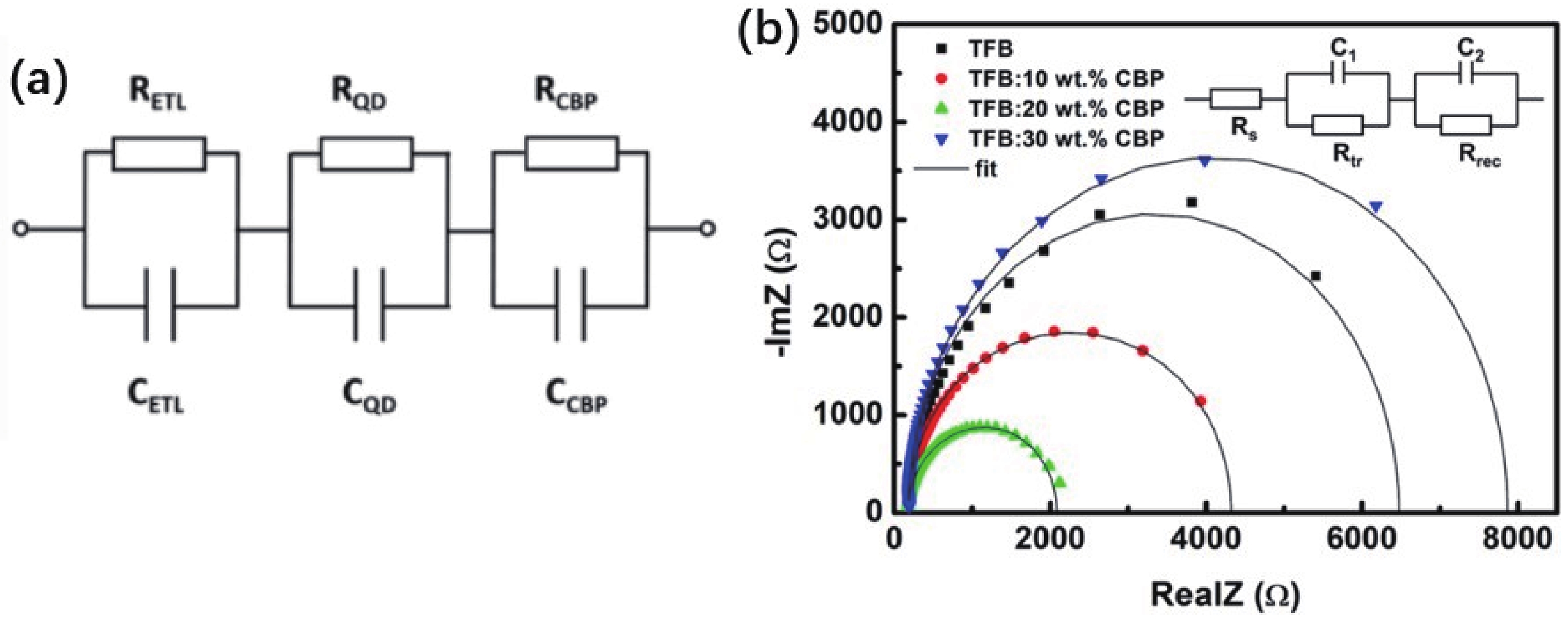
To accurately construct an equivalent circuit model of a QLED, each functional layer should be carefully considered into the circuit model. Xiao et al. proposed an equivalent circuit model that includes the circuit elements of R1, R2, RQD, R3, C1, and CQD[44], Here, R1, R2, RQD, and R3 are the resistances of the TFB, PEDOT: PSS, QD, and ZnO nanoparticle layers, respectively. C1 is the junction capacitance at the QD-TFB interface, while CQD is the capacitance of the QD layer. The junction capacitance at the QD-ZnO interface is not included in the proposed circuit because there is little electron accumulation at this interface. However, a large number of holes accumulate at the QD-TFB interface due to the large hole injection barrier, resulting in the formation of a junction capacitance C1. The electrical parameters of each circuit element and the carrier lifetime were further calculated in their study. As shown in Fig. 3(a), for an inverted QLED device, the equivalent circuit can be modeled with a series-connected resistance of ZnO, QD, and CBP (RETL, RQD, RCBP), and its parallel capacitance (CETL, CQD, CCBP)[45]. The geometrical capacitance was calculated to be 1.23 nF based on the dielectric constants of ZnO, QD, and CBP, which was close to the experimentally measured value of 1.38 nF, indicating that the charge injection at the contact is negligible.

Fig. 3.  (Color online) Equivalent circuit model of QLEDs based on (a) device structure, (b) the function of each circuit element. Modified with permission from (a) Ref. [45] Copyright 2022 Springer Nature, (b) Ref. [47] Copyright 2022 American Chemical Society.

The above conventional circuit models are based on the device structure, while other equivalent circuit models are developed by considering the function of each circuit element. As shown in Fig. 3(b), for example, the equivalent circuit of a QLED device can be modelled with a series resistance (Rs, contact resistance), transport resistance (Rtr) and its parallel transport capacitance (Ctr), recombination resistance (Rrec) and its parallel recombination capacitance (Crec)[46, 47], where Rs, Rtr, and Rrec can evaluate the charge injection efficiency, the charge transport capability, and recombination probability of a working device, respectively. For example, when TFB is mixed with CBP, the recombination resistance (Rrec) is reduced from 4080 to 1221 Ω, indicating an improved hole-electron recombination probability resulting from the HTL modification. Moreover, the charge injection can be studied by measuring the series resistance (Rs) at different temperatures. A decrease in temperature from 300 to 120 K resulted in a decrease in Rs from 85.6 to 33.7 Ω, suggesting an improved charge injection at lower temperature[48]. Therefore, an equivalent circuit model can provide valuable insights into the electrical and optical properties of charge transport layers, which can help in the design and optimization of QLED devices.

The impedance of a QLED device cannot always be accurately represented by a simple RC circuit model due to the non-ideal electrical processes that occur at the device[4954]. To account for this, the constant phase element (CPE) is often used to replace the capacitance in the circuit model. The impedance of CPE is defined as[29]

ZCPE=1Q(iω)n,
(6)

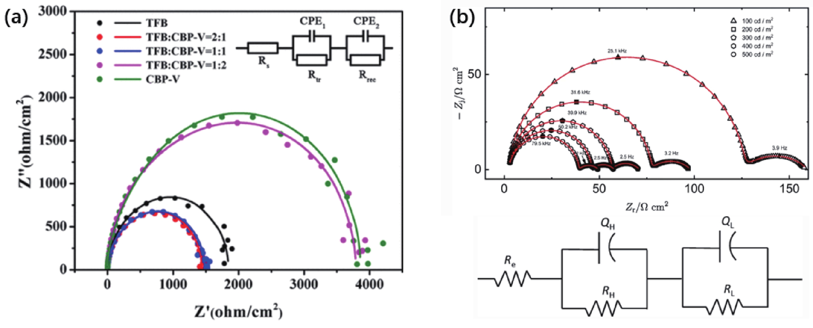
where n is a dispersion parameter that determines the physical meaning of Q. If n = 1, then Q = C; if n = 0, then Q = 1/R; if 0 < n < 1, then Q represents a non-ideal dielectric element, where the more n deviates from 1, the further Q deviates from a pure capacitor. Therefore, CPE is also widely employed in an equivalent circuit model. For the above equivalent circuit model consisting of the transport capacitance Ctr and the recombination capacitance Crec, as shown in Fig. 4(a), CPE is employed to replace the Ctr and Crec[4954], and the resistance of Rtr and Rrec in the circuit reflect the charge transport capability and charge recombination probability of QLED, which is suitable for imperfect physical process.

Fig. 4.  (Color online) (a) Equivalent circuit model of QLED based on CPE circuit element, (b) Nyquist plot of QLED with two semicircles and its equivalent circuit model. Modified with permission from (a) Ref. [54] Copyright 2020 American Chemical Society, (b) Ref. [55] Copyright 2022 Springer Nature.

A Nyquist plot with two semicircles characterizes a device with two relaxation processes, i.e., two charging time constants. As shown in Fig. 4(b), such a device's impedance can be fitted with two CPEs, one dominating at low frequency and the other at high frequency[55]. By fitting the data, the Q and n parameters can be extracted from the low and high-frequency regimes, and the effective and total capacitance can be calculated. Furthermore, the high-frequency part of the Nyquist plot is often attributed to the physical process in the hole-injection layer by comparing the electrical parameters of a QLED and a hole-only device.

Multiple equivalent circuit models can be built up based on different understandings of device physics and impedance responses. However, limitations exist in the application of Nyquist plots. For instance, there is not a unique equivalent circuit model for a given Nyquist plot, because the complex RC circuit can be simplified to a single RC circuit using Thevenin theorem. As a result, it is challenging to identify the individual relaxation processes for each RC element. Additionally, researchers may introduce many parameters to improve data fitting accuracy, but this can make it difficult to interpret the individual physical meaning of each circuit element. Therefore, the equivalent circuit model extracted from a Nyquist plot should be easily understood and interpretable.

The capacitance of a QLED is a complex function of frequency, as it is influenced by various charge dynamics, such as charge injection, recombination, and trapping, each characterized by a distinct time constant[12, 20, 32, 41, 48, 5660]. As a result, the capacitance of a QLED exhibits frequency-dependent variations, which can be attributed to the underlying charge behavior. In general, the accumulation of carriers will contribute to an increase in the device capacitance, while carrier recombination leads to a decrease in capacitance. Therefore, the capacitance of a QLED can be expressed as a sum of several components[60, 61], which includes the geometrical capacitance, the charge accumulation capacitance associated with the accumulation of injected carriers, and the charge recombination capacitance linked to the depletion of injected carriers via recombination. Hence, the total capacitance of a QLED can be written as:

C(ω)=Cg+CaccCrec=Cg+a1τacc1+(ωτacc)2a2τrec1+(ωτrec)2,
(7)

where Cg is the geometrical capacitance, Cacc is the capacitance rise induced by the charge accumulation, Crec is the capacitance drop caused by charge recombination, and τacc and τrec are the characteristic time constant for charge accumulation and recombination, respectively. a1 and a2 is the dimensionless constant for τacc and τrec, respectively. By fitting the Cω characteristics using the above equation, it is possible to extract the carrier accumulation and recombination time constants.

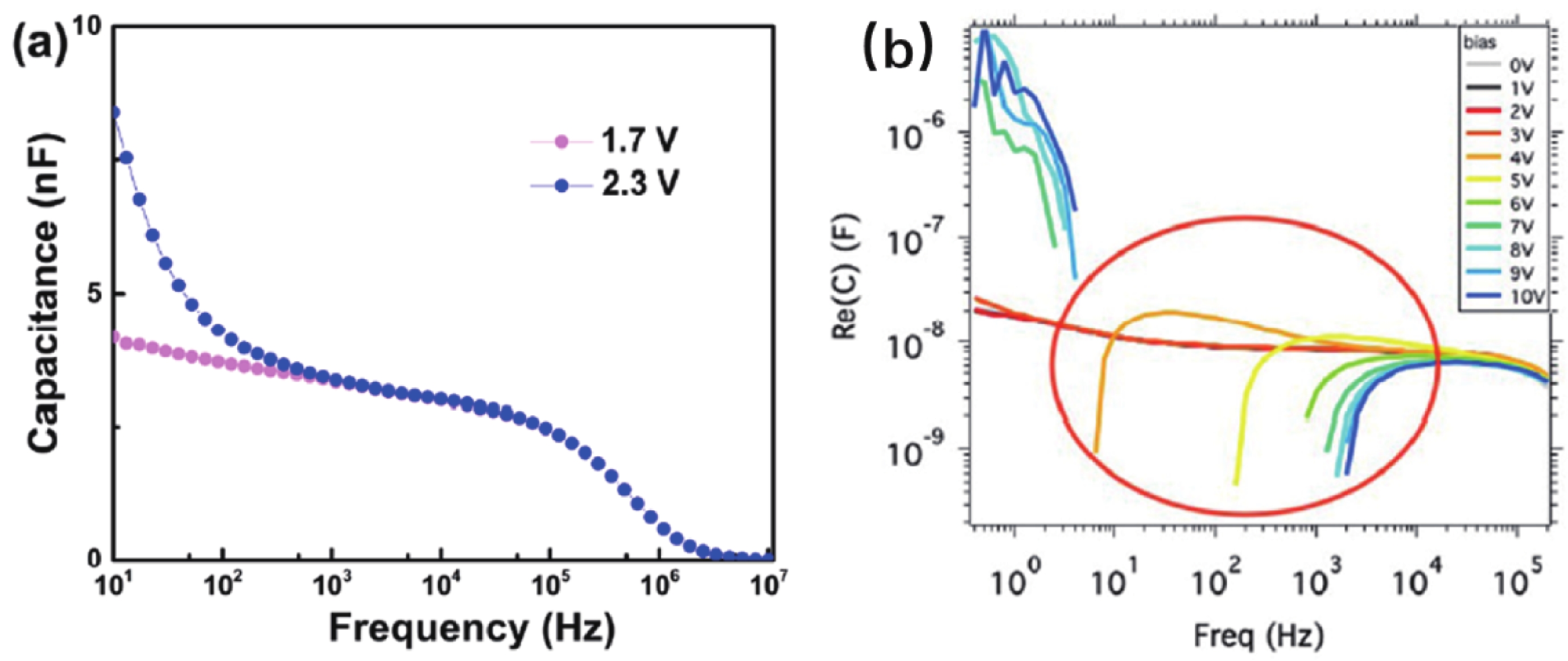
In this case, the Cf characteristics of QLEDs exhibit a strong dependence on the applied voltage. In brief, at a low bias before a QLED emits, the device capacitance is contributed by its geometrical capacitance Cg. While at high voltage after the device turns on, the charge accumulation and recombination have a significant contribution to the total capacitance. Furthermore, the characteristic time constants (τacc and τrec) vary with bias, thus determining the unique Cf characteristic of the QLED at the selected working voltage. As shown in Fig. 5(a), the capacitance of the blue QLED at low frequency at 2.3 V rises sharply compared to that at 1.7 V, which is owing to the charge injection. Moreover, in Fig. 5(b), researchers have compared the Cf characteristics of the purple QLED within the voltage range of 0 to 10 V. The capacitance of QLEDs before 3 V always remains positive. However, the capacitance of the purple QLED at the bias higher than 3 V becomes negative after the threshold frequency (f corresponded to C = 0 nF), indicating the charge recombination process dominates the device capacitance. On the other hand, the threshold frequency, peak capacitance and the shape of the Cf curve varies with different working voltages. Therefore, Cf characteristics of QLEDs is highly dependent on the working bias, necessitating a comprehensive investigation and discussion of their relationship.

Fig. 5.  (Color online) Capacitance−frequency characteristics of (a) blue QLED at 1.7 V and 2.3 V, (b) purple QLED within the voltage range from 0 to 10 V. Modified with permission from (a) Ref. [41] Copyright 2022 AIP Publishing, (b) Ref. [60] Copyright 2019 AIP Publishing.

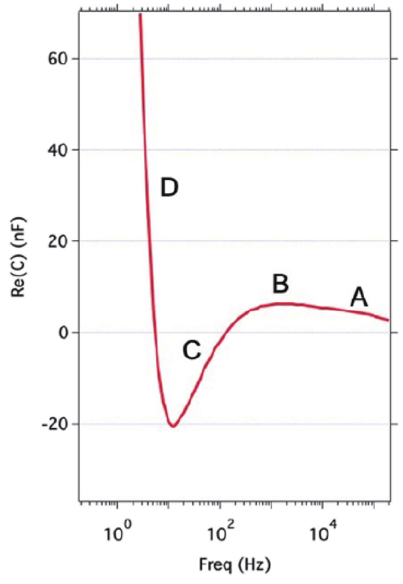
Blauth et al. have reported a distinct capacitance−frequency (Cf) characteristic of QLEDs compared to OLEDs[60]. Unlike OLEDs, QLEDs exhibit a decreasing capacitance from their geometrical capacitance at high frequency to a negative value at low frequency, which eventually returns to a positive value at very low frequency. This behavior is attributed to the complex interplay between charge injection, trapping, and recombination processes with distinct characteristic time constants, as governed by the device structure and materials. As shown in Fig. 6, at high frequency, the device capacitance of QLED behaves similarly to its geometrical capacitance, as no significant charge injection or trapping occurs. As the frequency decreases, charges start to inject into the device and accumulate in traps, leading to a rise in capacitance. At even lower frequencies, the charge recombination and light out-coupling processes occur, depleting the carriers and resulting in a drop in capacitance. However, as the frequency approaches very low values, the charges become more fixed and occupy the trap states, causing the device capacitance to rise again and return to a positive value. This distinct Cf behavior of QLEDs is determined by the characteristic time constants for charge accumulation, recombination, and trapping, which are different from those of OLEDs. The interplay between these processes, together with the device structure and materials, results in the observed capacitance−frequency characteristics of QLEDs.

Fig. 6.  (Color online) Capacitance−frequency characteristic of the QLED. Modified with permission from Ref. [60] Copyright 2019 AIP Publishing.

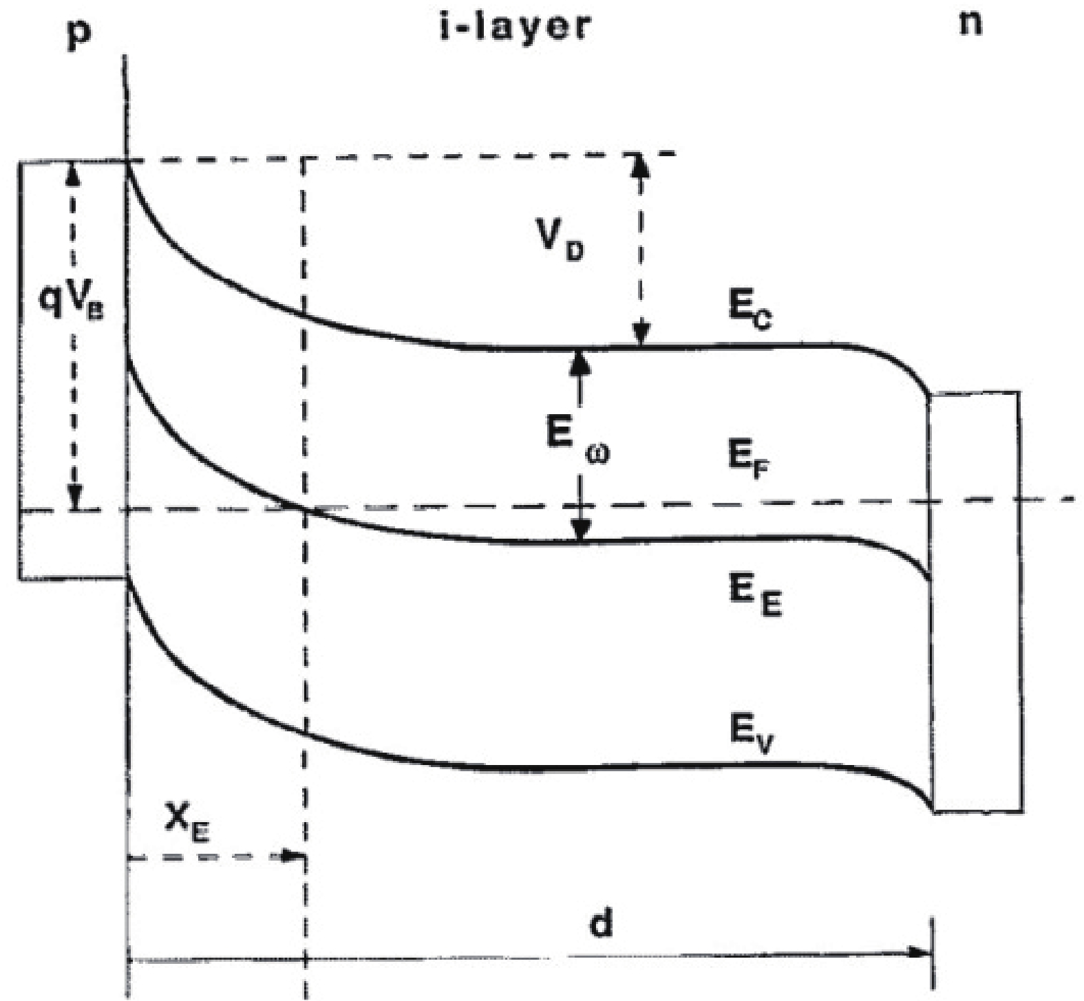
In addition, the Cf characteristics can also be used to calculate the trap distribution if the additional capacitance is solely contributed by carrier trapping[62, 63]. This technique is commonly referred to as defect spectroscopy. As depicted in Fig. 7, for a heterojunction, the carrier trapping time constant can be expressed as[29, 62, 63]

Fig. 7.  Energy level of a p−i−n heterojunction. Modified with permission from Ref. [37] Copyright 1992 AIP Publishing.
τ=γ1exp(ΔEkT),
(8)

where γ is the attempt to escape frequency, ∆E is the energy difference between the trap state and the band edge, k is the Boltzmann constant, and T is the temperature. Thus, the trap state E(ω) at a selected ω can be determined. Specifically, γ represents the maximum angular frequency that the carrier occupied trap state in the voltage modulation. Then, E(ω) in Fig. 6 is given by[29, 62, 63]

E(ω)=kTln(γω).
(9)

Thus, only when ω < γ can the carrier occupy the trap state and cause the capacitance rise. The smaller the ω, the deeper the occupied trap state. Consequently, a shallow trap state can be occupied at a higher frequency, whereas a deep trap state requires a low frequency.

Moreover, the density of states is proportional to the derivative of the device capacitance with respect to angular frequency, which can be expressed as[29, 62, 63]

N(E(ω))=VbiqWdCdωωkT,
(10)

where Vbi is the built-in voltage, q is the elementary charge, and W is the depletion width. Hence, the trap distribution can be determined by the Cf characteristic of the QLED.

In a red QLED, the trap state distribution changes as temperature varies. Typically, as the temperature rises, the trap state becomes higher, but the density of the state becomes smaller. Furthermore, researchers have observed the broadening of the DOS distribution with a higher temperature. Therefore, a temperature-dependent trap distribution is studied by the Cf characteristics of the red QLED[48]. When QD was modified by a PMMA mixture, the density of the trap state was effectively reduced by 1% PMMA content, as per the Cf characteristic of the QLED[57]. In a blue QLED, the trap state close to the conduction band minimum is reported to assist the electron injection. In addition to calculating the captured electron density by traps, the trap distribution is estimated by the Cf characteristics of the pristine and electrically aged device[41]. Furthermore, the trap density of the QLED can be monitored by the Cf characteristics during the QLED operation process. Researchers compared the trap density of ink-jet printed QLED with different ligands[12]. As a result, the trap formation was significantly suppressed by a bifunctional ligand Zn(OA)2, which showed a better trap passivation effect.

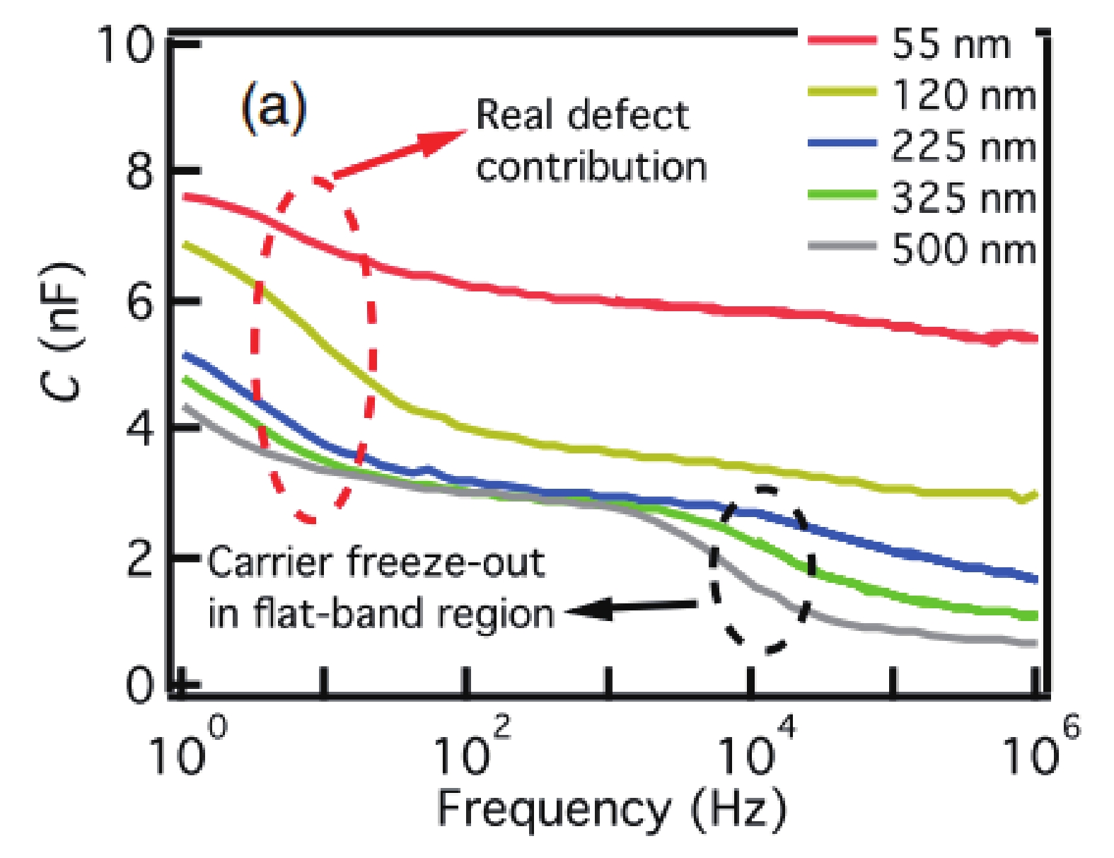
However, to estimate the trap distribution by the Cf characteristic of the device, the capacitance rise should be solely attributed to carrier trapping. For instance, Xu et al. observed the capacitance rise of OPV in a Cf characteristic[64]. As shown in Fig. 8, at low frequency, the capacitance rise came from the real defect contribution, while the capacitance at high frequency was attributed to the carrier freeze-out in the flat-band region, which cause the device capacitance transition from geometrical capacitance to junction capacitance. Thus, it is necessary to confirm the source of the additional capacitance; otherwise, it may lead to the misapplication of defect spectroscopy.

Fig. 8.  (Color online) Capacitance−frequency characteristics of OPV with two-step capacitance rise. Modified with permission from Ref. [64] Copyright 2016 American Physical Society.

The Nyquist plot and Cf characteristics are commonly used to determine the electrical properties of QLEDs, including the relaxation time constant and the electronic structure of materials and heterojunctions. However, these methods only provide information about the electrical behavior of a QLED device at a specific working voltage. Here, we introduce the CV characteristic of a QLED, which can track the working point in a JV characteristic curve, allowing for analysis of charge dynamics across a wide range of voltages. The capacitance of a QLED can be defined as the change in the amount of charge induced by a voltage perturbation, which can be expressed as[32]

C=dQdV=dQm+dQaccdQrecdvac.
(11)

The total charge amount Q is composed of Qm, the charge amount associated with the electrode charging process; Qacc, the accumulated charge amount induced by charge injection; and Qrec, the consumed charge amount caused by charge recombination.

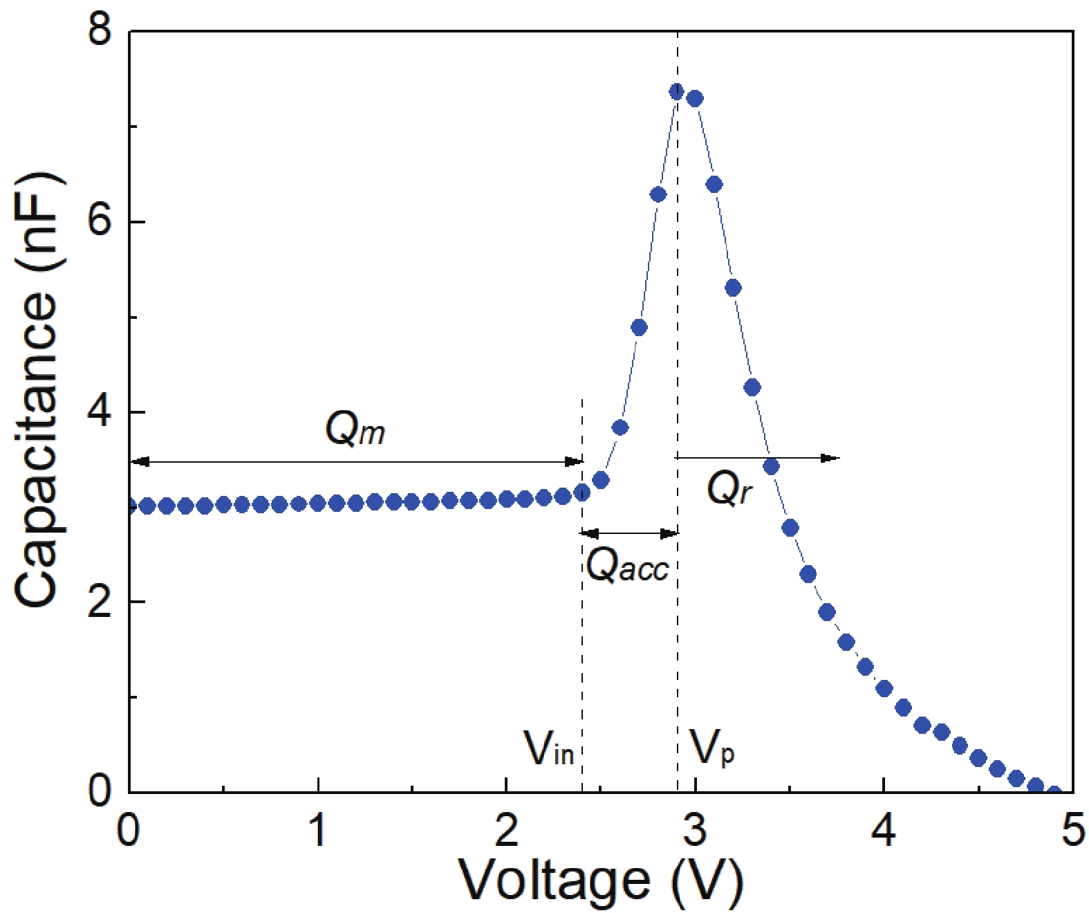
Fig. 9 displays the CV characteristic of a blue QLED. At low applied voltages, the capacitance is dominated by the electrode charging process, and no charge is injected into the device. Therefore, the capacitance is determined by the geometrical capacitance, which can be calculated as[29, 30, 32, 34]

Fig. 9.  (Color online) Capacitance−voltage characteristic of a blue QLED.
Cg=ε0εrAd,
(12)

where ε0 is the vacuum permittivity, εr is the relative permittivity of the QLED, A is the active area, and d is the thickness of the QLED. As the applied voltage increases to Vin, the capacitance begins to rise, indicating electron injection and accumulation in the QD emission layer. When the voltage reaches Vp (the voltage at peak capacitance), holes start to inject into the QD layer, and electron-hole recombination dominates the CV characteristics. This process depletes the accumulated carriers and causes a sharp drop in the device capacitance[6585]. Therefore, the characteristic voltages (Vin and Vp) represent the electron and hole injection points, which can be used to compare the charge injection capability of the charge transport layer.

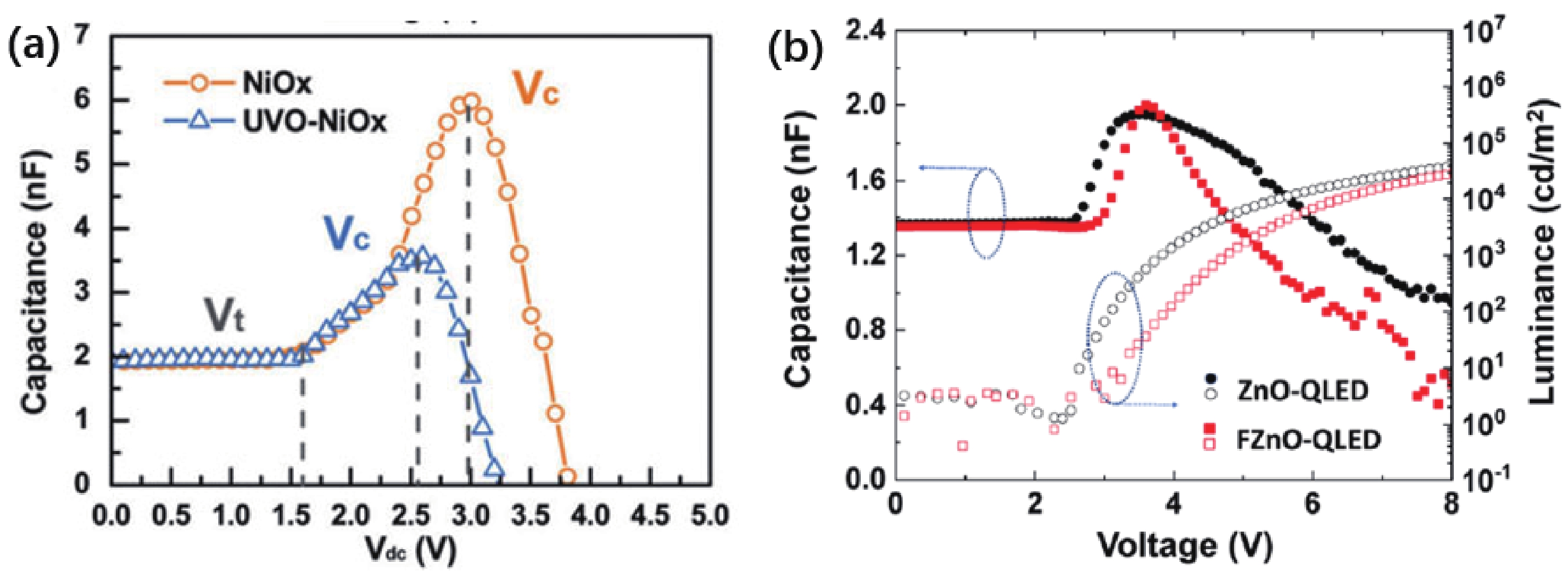
Modifying the functional layer can sensitively affect the characteristic voltages Vin and Vp, reflecting changes in the charge injection point and capability. As shown in Fig. 10(a), when the hole injection layer NiO film is treated with the UV-ozone, Vin remains the same as in the pristine device, while Vp is smaller, indicating that the UV-ozone treatment did not affect electron injection but significantly facilitated hole injection[75]. When the ZnO layer was treated with CF4 plasma, the electron injection capability was weakened, as shown in Fig. 10(b), the characteristic voltages Vin and Vp of the CF4-treated device were both larger than those of the pristine device[45]. These results support the charge injection points exhibited in the CV characteristic well.

Fig. 10.  (Color online) (a) Capacitance−voltage characteristics of (a) pristine device and UV-ozone treated device, (b) pristine device and CF4-treated device. Modified with permission from (a) Ref. [75] Copyright 2019 RSC Pub, (b) Ref. [45] Copyright 2022 Springer Nature.

However, it has been noted in some studies that the characteristic voltage Vin is close to the turn-on voltage of QLED[20, 86], indicating that capacitance rise and charge recombination occur simultaneously. In such cases, Vin may also represent the charge recombination point in the CV characteristic, indicating that both electrons and holes are injected into the device simultaneously. Therefore, further investigation is needed to fully understand the physical meaning of CV characteristics.

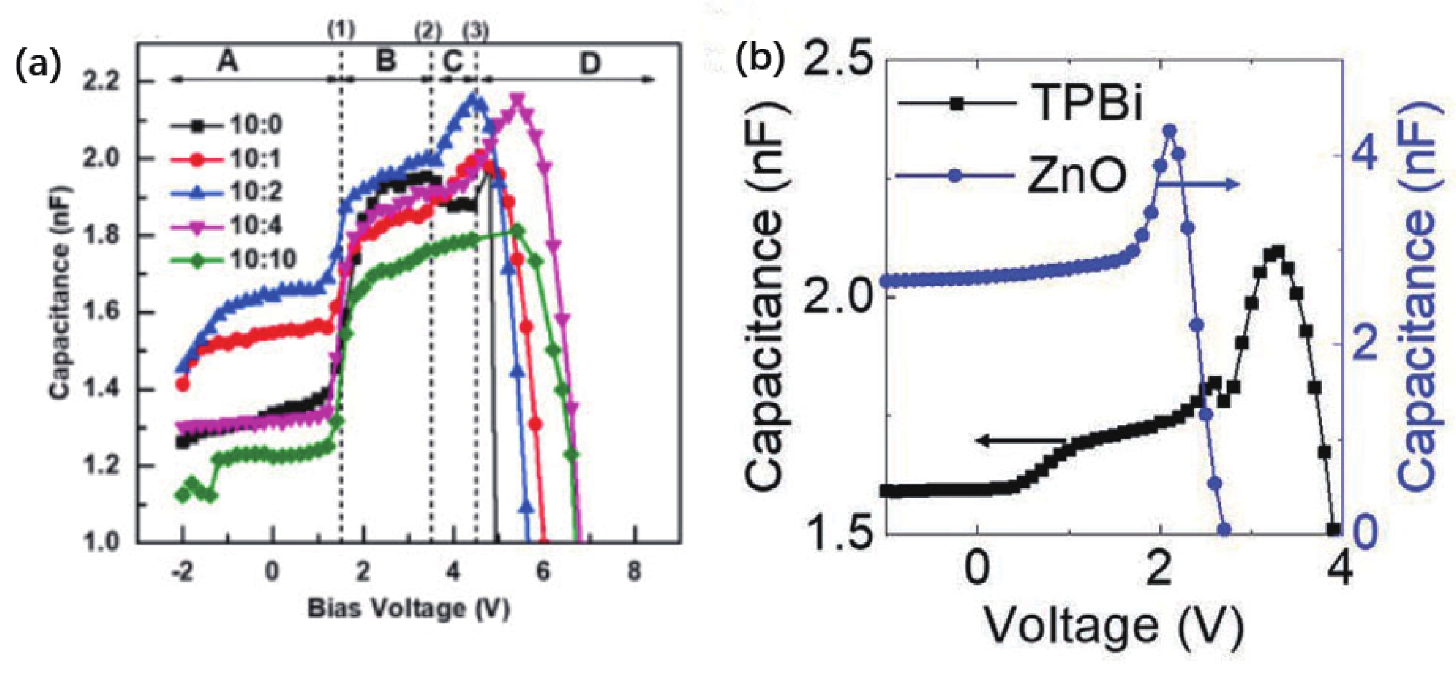
On the other hand, some researchers have observed two steps in the capacitance rise before the peak capacitance, with the first rise indicating majority carrier injection, and the second indicating minority carrier injection[20, 53]. As shown in Fig. 11(a), for an inverted QLED structured as ITO/ZnO/QD/TAPC/WO3/Ag, the device capacitance first rose at 1.5 V, indicating electron injection. The second rise point of the device capacitance was around 3.5 V, reflecting the hole injection point. As the applied bias increased further, the device capacitance exhibited a steeper rise due to both electron and hole injection[53]. In our previous study, we found that the QD layer was negatively charged at the initial stage, promoting hole injection and rejecting electron injection. As a result, in a normal QLED with the TPBi ETL, the hole injection starts at low applied bias while electron injection starts at higher working voltage (Fig. 11(b)), resulting in two capacitance rise processes in the CV characteristic[20]. However, when the ETL is replaced by ZnO nanoparticles, the charge in the QD layer is transferred to the ZnO ETL, making the QD layer neutral. In this case, the voltage at capacitance rise is close to the turn-on voltage, indicating that both electrons and holes are injected at the same time. Therefore, the shape of the CV curve is distinct for different charge injection cases.

Fig. 11.  (Color online) (a) Capacitance−voltage characteristics of (a) the inverted QLED, (b) normal QLED with ZnO and TPBi ETLs. Modified with permission from (a) Ref. [53] Copyright 2022 Elsevier Ltd and (b) Ref. [20] Copyright 2021 Wiley-VCH Verlag GmbH & Co. KGaA.

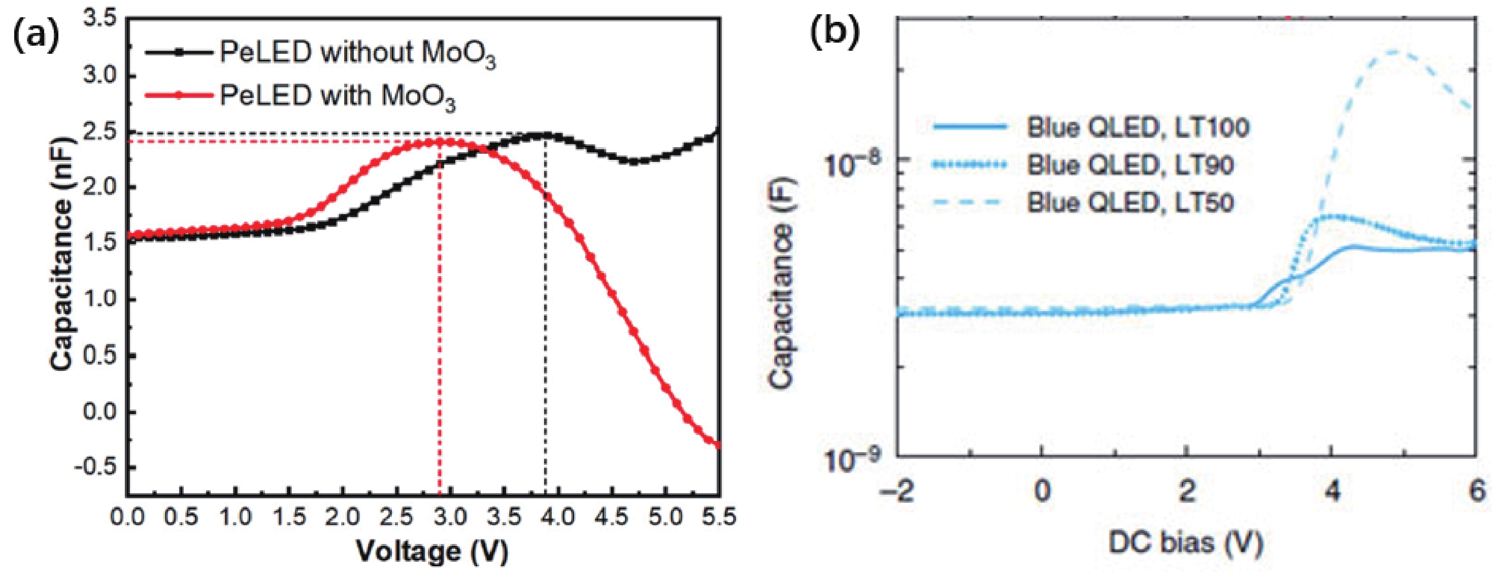
Moreover, the capacitance rise and drop rates reflect the charge injection and recombination efficiency[45, 87]. A faster drop rate typically indicates a more effective charge recombination process, which can help analyze the charge recombination rate. As shown in Fig. 12 (a), when an ultrathin MoO3 interlayer is added between PEDOT: PSS and PVK, the hole injection capability is enhanced, resulting in more balanced charge injection in perovskite QLED. Consequently, the reduced characteristic voltage Vin and faster capacitance drop are exhibited in the CV characteristic of the MoO3-modified device[87].

Fig. 12.  (Color online) (a) Capacitance−voltage characteristics of (a) pristine QLED and MoO3-modified QLED, (b) blue QLED at different degradation periods. Modified with permission from (a) Ref. [87] Copyright 2022 AIP Publishing, (b) Ref. [21] Copyright 2019 Springer Nature.

The peak capacitance observed in a CV characteristic provides information about the amount of accumulated charge in a QLED[21, 22, 83, 88]. As such, it is a useful technique for investigating the degradation mechanism of QLEDs. As shown in Fig. 12(b), when the luminance of the blue QLED has degraded to 50% of its initial value, the peak capacitance becomes equal to the geometrical capacitance of the ZnO nanoparticle layer. This indicates that the HTL has reached the flat-band condition, leaving the applied voltage concentrated across the ETL. Consequently, the electrons accumulate in the ZnO layer, leading to the degradation of the QLED[21]. In addition, CV characteristics are also sensitive to the presence of traps in the device, making them suitable for confirming trap formation during QLED operation. For example, a comparison of the CV characteristics of red QLEDs based on a ZnSe or ZnS shell reveals a decreased peak capacitance in the ZnS shelled QLED, implying the trap formation of the ZnS shell QLED during the lifetime measurement[11].

Therefore, CV characteristics can be used to extract physical information about the charge injection, accumulation, and recombination in a QLED over a wide voltage range, facilitating the analysis of QLED performance loss and degradation mechanisms. However, for effective CV analysis, the selected frequency must ensure that the charge injection and accumulation occur within the measurement frequency range. Therefore, the frequency cannot be too high, or else the charge will not respond to the alternating signal[20, 86]. Furthermore, if a QLED exhibits serious charge leakage, it is difficult to observe the capacitance rise in a CV characteristic, in this case, the charge injection point is hard to extract[89].

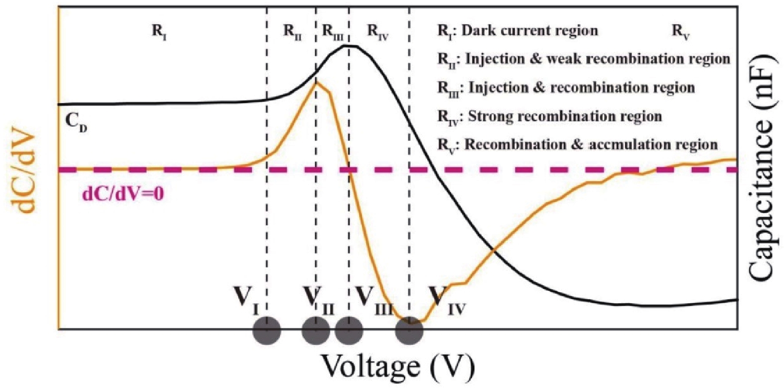
A technique, known as the dC/dV measurement, has been developed to supplement the information obtained from the CV curve in a QLED[86, 90]. Fig. 13 presents both the CV and its first-derivative dC/dVV characteristics of a red QLED in a single figure.

Fig. 13.  (Color online) Capacitance−voltage and dC/dVV characteristics of a red QLED. Modified with permission from Ref. [86] Copyright 2022 IOP Publishing.

1) Region Ⅰ, as shown in Fig. 13, represents a state where dC/dV = 0, indicating that the device's capacitance remains constant. In this case, there is no charge injection into the QLED, and the capacitance is contributed only by its geometrical capacitance.

2) Region Ⅱ is characterized by a positive slope of dC/dV, indicating a rise in capacitance due to charge injection. Additionally, in this voltage range, the device is lighted, indicating simultaneous charge recombination. However, the charge amount induced by charge injection exceeds the charge recombination, and charge accumulation dominates.

3) In region Ⅲ, dC/dV still has a positive slope, but the slope decreases, indicating an increase in charge recombination that consumes carriers.

4) Region Ⅳ is marked by a negative slope of dC/dV, implying that charge injection is dominating in this voltage range. The capacitance is decreasing from its peak value, indicating a high carrier consumption. Particularly, the characteristic voltage V corresponds to the minimum value of dC/dV, which is close to the voltage at the maximum EQE, suggesting that the best charge balance is achieved in this voltage range.

5) Finally, in region Ⅴ, the slope of dC/dV becomes increasingly negative as the applied voltage increases, indicating that the charge recombination rate tends towards saturation while the charge injection rate remains unaffected.

The use of a dC/dV measurement in impedance spectroscopy provides additional information on the charge dynamics of a QLED, which supplements the information obtained from the CV characteristics. The slope change of the dC/dV curve reflects the change in charge injection and recombination rate, and the voltage at which the minimum dC/dV value occurs provides insight into the maximum EQE point. The dC/dV measurement is also applicable to silicon-based QLEDs[90], where the negative peak value of dC/dV indicates a fast capacitance decay rate. Therefore, a dC/dV measurement is a crucial tool for investigating the charge dynamics of QLEDs.

Mott–Schottky analysis is a well-known method for determining the doping density and built-in voltage of optoelectronic devices[6, 9195]. This method describes the dependence of the 1/C2 on applied voltage, which is given by[91]

1C2=2qϵA2NA(VbiV).
(13)

Here, C represents the capacitance of the device, q is the elementary charge, ε is the dielectric constant, A is the active area, NA is the total doping density, and Vbi is the built-in voltage. the built-in voltage and doping density can be determined according to the slope and intercept of the curve. The Mott−Schottky equation is built up based on the depletion of the space charge region in a PN junction, so the depletion approximation must be satisfied in a device.

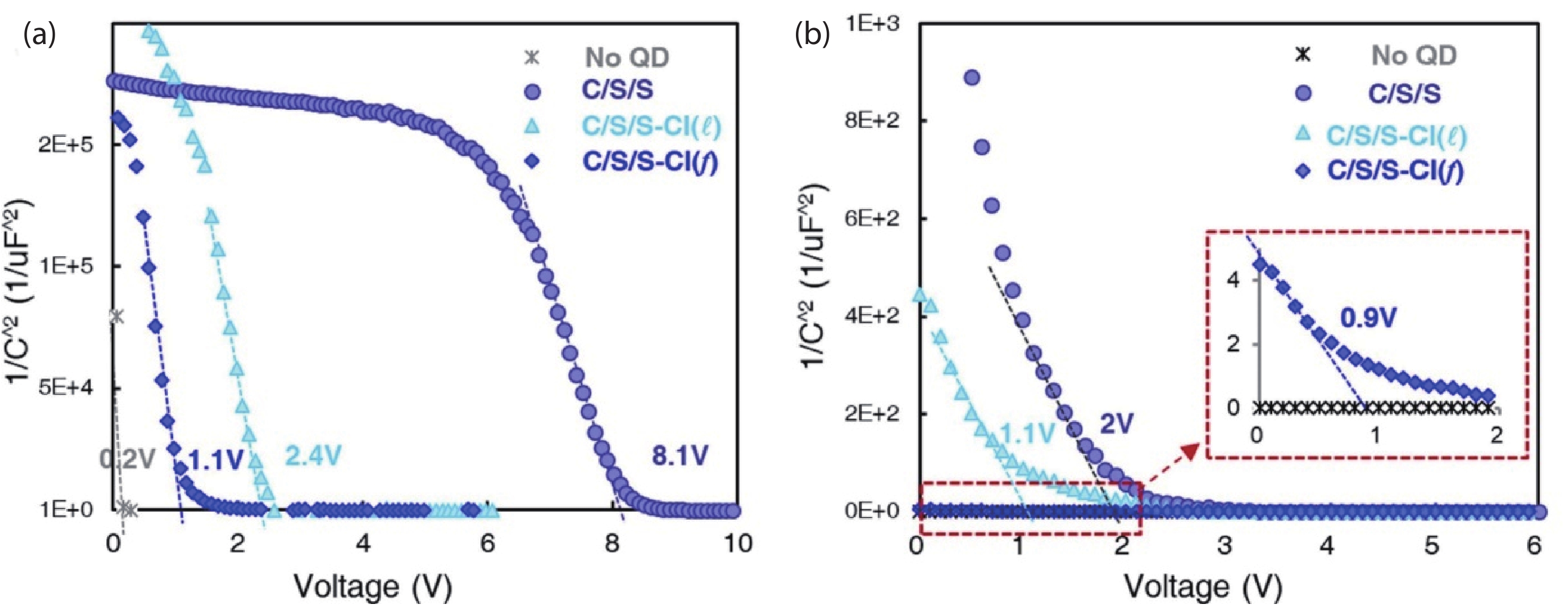
Fig. 14 illustrates the 1/C2V characteristics of an electron-only device (EOD) and hole-only device (HOD) based on ZnSeTe QDs[6]. Ligand exchange was employed to improve the electron and hole injection in the devices. The built-in voltage of the HOD decreased from 8.1 to 2.4 V with solution ligand exchange and to 1.1 V with film ligand exchange. Similarly, the built-in voltage of the EOD decreased from 2.0 to 0.9 V with the two-step ligand exchange. The results demonstrate that the two-step ligand exchange process improves both electron and hole injection, enabling efficient and stable blue QLEDs.

Fig. 14.  (Color online) 1/C2V characteristics of the HOD (a) and EOD (b). Modified with permission from Ref. [6] Copyright 2020 Springer Nature.

Moreover, the built-in voltage of the EOD and HOD can be used to analyze the majority carrier in QLED devices. For the CdSe-based blue QLED, the dominant carrier is not clear. Using Mott–Schottky analysis, the built-in voltage of the EOD was found to be smaller than that of the HOD, indicating that the blue QLED is an electron-dominated device[96]. This result provides a guide for improving the performance of blue QLEDs by optimizing the charge injection process. The Mott–Schottky analysis is thus a useful tool for impedance analysis of single-carrier devices.

The applications and limitations of these impedance measurements are summarized in Table 1, which provides supplementary data analysis for a JV characteristic of the QLED. Overall, impedance spectroscopy is a powerful tool that enables the characterization of various aspects of QLEDs, providing a better understanding of their behavior and performance. Usually, to analyze the charge dynamics of the QLED, these impedance spectroscopy characteristics are recommended to be combined to provide a full insight into the device physics. For example, traps play an important role in charge injection and the charge recombination process, an additional capacitance induced by traps may affect the shape of the Nyquist plot, and the capacitance in the equivalent circuit model may consist of both geometrical capacitance and additional capacitance, the charge injection point and charge recombination rate are also affected by defects in the CV characteristic. Additionally, the trap distribution can be calculated from the Cf characteristic. When an interlayer is introduced in a QLED, an RC circuit of the interlayer may be added to the pristine equivalent circuit model, and the electrical parameters of the circuit element can be extracted to analyze the effect of the interlayer. Similarly, the charge injection point in a CV characteristic reflects the charge injection capability of the interlayer. Furthermore, optical spectra such as photoluminescence and absorption also provide physical information on carrier behavior upon optical excitation. Therefore, a combination of JV characteristics, impedance spectroscopy, and optical spectra analysis provides a comprehensive characterization method for analyzing the optical and electrical properties of the material, interface, and the entire QLED device.

Table 1.  The applications and limitations of the impedance measurement.
Application Limitation
Nyquist plot Charging time constant, equivalent circuit model. Many equivalent circuit models correspond to one Nyquist plot, so the physical meaning of each circuit element should be clear.
Cf characteristic The characteristic time constant for charge accumulation and recombination; trap distribution. The capacitance rise is only contributed to the carrier trapping for the defect spectroscopy.
CV characteristic Charge injection point, charge injection and recombination rate. The frequency is required to satisfy the charge response to the alternating signal.
dC/dVV characteristic The characteristic voltage at maximum EQE, Supplementary information to CV characteristics
Mott−Schottky analysis (1/C2V characteristic) Doping density, built-in voltage Depletion approximation must be satisfied in a device.
DownLoad: CSV  | Show Table

In this review, we have examined the utility of impedance spectroscopy in the context of QLEDs. We have covered the fundamental mathematical principles underlying impedance spectroscopy, the methodology for analyzing impedance data, examples of impedance spectroscopy in QLEDs, and the limitations of this technique. In general, the Nyquist plot provides a powerful means of constructing an equivalent circuit model for QLEDs, while the Cf characteristic can be used to extract key parameters such as the characteristic time constant and trap distribution. These impedance measurements provide valuable insights into the physical behavior of QLEDs for a given working voltage. Additionally, the CV characteristic of a QLED can be used to track the working voltage of the JV characteristic, providing a more comprehensive understanding of the charge dynamics in QLEDs. Overall, this review presents a useful toolbox of impedance spectroscopy techniques for researchers interested in studying the device physics of QLEDs and related fields.

This work was supported by National Key Research and Development Program of China (Nos. 2021YFB3602703, 2022YFB3606504, and 2022YFB3602903), Shenzhen Key Laboratory for Advanced Quantum Dot Displays and Lighting (No. ZDSYS201707281632549), and Shenzhen Science and Technology Program (No. JCYJ20220818100411025).


[1]
Colvin V L, Schlamp M C, Alivisatos A P. Light-emitting diodes made from cadmium selenide nanocrystals and a semiconducting polymer. Nature, 1994, 370, 354 doi: 10.1038/370354a0
[2]
Dai X L, Zhang Z X, Jin Y Z, et al. Solution-processed, high-performance light-emitting diodes based on quantum dots. Nature, 2014, 515, 96 doi: 10.1038/nature13829
[3]
Shen H B, Gao Q, Zhang Y B, et al. Visible quantum dot light-emitting diodes with simultaneous high brightness and efficiency. Nat Photonics, 2019, 13, 192 doi: 10.1038/s41566-019-0364-z
[4]
Deng Y Z, Peng F, Lu Y, et al. Solution-processed green and blue quantum-dot light-emitting diodes with eliminated charge leakage. Nat Photonics, 2022, 16, 505 doi: 10.1038/s41566-022-00999-9
[5]
Song J J, Wang O Y, Shen H B, et al. Quantum dot LEDs: Over 30% external quantum efficiency light-emitting diodes by engineering quantum dot-assisted energy level match for hole transport layer. Adv Funct Mater, 2019, 29, 1970226 doi: 10.1002/adfm.201970226
[6]
Kim T, Kim K H, Kim S, et al. Efficient and stable blue quantum dot light-emitting diode. Nature, 2020, 586, 385 doi: 10.1038/s41586-020-2791-x
[7]
Qian L, Zheng Y, Xue J G, et al. Stable and efficient quantum-dot light-emitting diodes based on solution-processed multilayer structures. Nat Photonics, 2011, 5, 543 doi: 10.1038/nphoton.2011.171
[8]
Shirasaki Y, Supran G J, Bawendi M G, et al. Emergence of colloidal quantum-dot light-emitting technologies. Nat Photonics, 2013, 7, 13 doi: 10.1038/nphoton.2012.328
[9]
Zhang Z X, Ye Y X, Pu C D, et al. High-performance, solution-processed, and insulating-layer-free light-emitting diodes based on colloidal quantum dots. Adv Mater, 2018, 30, e1801387 doi: 10.1002/adma.201801387
[10]
Mashford B S, Stevenson M, Popovic Z, et al. High-efficiency quantum-dot light-emitting devices with enhanced charge injection. Nat Photonics, 2013, 7, 407 doi: 10.1038/nphoton.2013.70
[11]
Cao W R, Xiang C Y, Yang Y X, et al. Highly stable QLEDs with improved hole injection via quantum dot structure tailoring. Nat Commun, 2018, 9, 2608 doi: 10.1038/s41467-018-04986-z
[12]
Xiang C Y, Wu L J, Lu Z Z, et al. High efficiency and stability of ink-jet printed quantum dot light emitting diodes. Nat Commun, 2020, 11, 1646 doi: 10.1038/s41467-020-15481-9
[13]
Pu C D, Dai X L, Shu Y F, et al. Electrochemically-stable ligands bridge the photoluminescence-electroluminescence gap of quantum dots. Nat Commun, 2020, 11, 937 doi: 10.1038/s41467-020-14756-5
[14]
Zhao J Y, Chen L X, Li D Z, et al. Large-area patterning of full-color quantum dot arrays beyond 1000 pixels per inch by selective electrophoretic deposition. Nat Commun, 2021, 12, 4603 doi: 10.1038/s41467-021-24931-x
[15]
Jia S Q, Tang H D, Ma J R, et al. High performance inkjet-printed quantum-dot light-emitting diodes with high operational stability. Adv Opt Mater, 2021, 9, 2101069 doi: 10.1002/adom.202101069
[16]
Liu D Q, Cao S, Wang S Y, et al. Highly stable red quantum dot light-emitting diodes with long T95 operation lifetimes. J Phys Chem Lett, 2020, 11, 3111 doi: 10.1021/acs.jpclett.0c00836
[17]
Chen X T, Lin X F, Zhou L K, et al. Blue light-emitting diodes based on colloidal quantum dots with reduced surface-bulk coupling. Nat Commun, 2023, 14, 284 doi: 10.1038/s41467-023-35954-x
[18]
Yu P L, Yuan Q L, Zhao J L, et al. Electronic and excitonic processes in quantum dot light-emitting diodes. J Phys Chem Lett, 2022, 13, 2878 doi: 10.1021/acs.jpclett.2c00604
[19]
Kim S K, Kim Y S. Charge carrier injection and transport in QLED layer with dynamic equilibrium of trapping/de-trapping carriers. J Appl Phys, 2019, 126, 035704 doi: 10.1063/1.5109089
[20]
Wu Z H, Liu P, Qu X W, et al. Identifying the surface charges and their impact on carrier dynamics in quantum-dot light-emitting diodes by impedance spectroscopy. Adv Opt Mater, 2021, 9, 2100389 doi: 10.1002/adom.202100389
[21]
Chen S, Cao W R, Liu T L, et al. On the degradation mechanisms of quantum-dot light-emitting diodes. Nat Commun, 2019, 10, 765 doi: 10.1038/s41467-019-08749-2
[22]
Qu X W, Ma J R, Liu P, et al. On the voltage behavior of quantum dot light-emitting diode. Nano Res, 2023, 16, 5511 doi: 10.1007/s12274-022-5106-8
[23]
Doe T, Kitano K, Yamamoto S, et al. Evaluation of degradation behavior in quantum dot light-emitting diode with different hole transport materials via transient electroluminescence. Appl Phys Lett, 2021, 118, 203503 doi: 10.1063/5.0041689
[24]
Su Q, Sun Y Z, Zhang H, et al. Quantum dots: Origin of positive aging in quantum-dot light-emitting diodes. Adv Sci, 2018, 5, 1870058 doi: 10.1002/advs.201870058
[25]
Acharya K P, Titov A, Hyvonen J, et al. High efficiency quantum dot light emitting diodes from positive aging. Nanoscale, 2017, 9, 14451 doi: 10.1039/C7NR05472F
[26]
Chen Z N, Su Q, Qin Z Y, et al. Effect and mechanism of encapsulation on aging characteristics of quantum-dot light-emitting diodes. Nano Res, 2021, 14, 320 doi: 10.1007/s12274-020-3091-3
[27]
Ding S, Wu Z, Qu X, et al. Impact of the resistive switching effects in ZnMgO electron transport layer on the aging characteristics of quantum dot light-emitting diodes. Appl Phys Lett, 2020, 117, 093501 doi: 10.1063/5.0019140
[28]
Chen D S, Chen D, Dai X L, et al. Shelf-stable quantum-dot light-emitting diodes with high operational performance. Adv Mater, 2020, 32, 2006178 doi: 10.1002/adma.202006178
[29]
Von Hauff E. Impedance spectroscopy for emerging photovoltaics. J Phys Chem C, 2019, 123, 11329 doi: 10.1021/acs.jpcc.9b00892
[30]
Nowy S, Ren W, Elschner A, et al. Impedance spectroscopy as a probe for the degradation of organic light-emitting diodes. J Appl Phys, 2010, 107, 054501 doi: 10.1063/1.3294642
[31]
Pingree L S C, Scott B J, Russell M T, et al. Negative capacitance in organic light-emitting diodes. Appl Phys Lett, 2005, 86, 073509 doi: 10.1063/1.1865346
[32]
Zhang L, Nakanotani H, Adachi C. Capacitance-voltage characteristics of a 4, 4’-bis [(N-carbazole)styryl]biphenyl based organic light-emitting diode: Implications for characteristic times and their distribution. Appl Phys Lett, 2013, 103, 093301 doi: 10.1063/1.4819436
[33]
Iván Mora-Seró, Germà Garcia-Belmonte, Pablo P Boix, et al. Impedance spectroscopy characterisation of highly efficient silicon solar cells under different light illumination intensities. Energy Environ Sci, 2009, 2, 678 doi: 10.1039/b812468j
[34]
Guerrero A, Bisquert J, Garcia-Belmonte G. Impedance spectroscopy of metal halide perovskite solar cells from the perspective of equivalent circuits. Chem Rev, 2021, 121, 14430 doi: 10.1021/acs.chemrev.1c00214
[35]
Von Hauff E, Klotz D. Impedance spectroscopy for perovskite solar cells: Characterisation, analysis, and diagnosis. J Mater Chem C, 2022, 10, 742 doi: 10.1039/D1TC04727B
[36]
Suresh M S. Measurement of solar cell parameters using impedance spectroscopy. Sol Energy Mater Sol Cells, 1996, 43, 21 doi: 10.1016/0927-0248(95)00153-0
[37]
Hegedus S S, Fagen E A. Midgap states in a-Si: H and a-SiGe: H p-i-n solar cells and Schottky junctions by capacitance techniques. J Appl Phys, 1992, 71, 5941 doi: 10.1063/1.350444
[38]
Taberna P L, Simon P, Fauvarque J F. Electrochemical characteristics and impedance spectroscopy studies of carbon-carbon supercapacitors. J Electrochem Soc, 2003, 150, A292 doi: 10.1149/1.1543948
[39]
Srinivasan R, Fasmin F. An Introduction to Electrochemical Impedance Spectroscopy. CRC Press, 2021 doi: doi.org/10.1201/9781003127932
[40]
Bao H, Chen C L, Cao Y Q, et al. Quantitative determination of charge accumulation and recombination in operational quantum dots light emitting diodes via time-resolved electroluminescence spectroscopy. J Phys Chem Lett, 2023, 14, 1777 doi: 10.1021/acs.jpclett.3c00070
[41]
Qu X W, Ma J R, Shan C W, et al. Trap state-assisted electron injection in blue quantum dot light-emitting diode. Appl Phys Lett, 2022, 121, 113507 doi: 10.1063/5.0104341
[42]
Park Y, Klöckner B, Hahm D, et al. Origin of enhanced efficiency and stability in diblock copolymer-grafted Cd-free quantum dot-based light-emitting diodes. J Mater Chem C, 2021, 9, 10398 doi: 10.1039/D1TC02534A
[43]
Yu P L, Zhu X X, Bai J L, et al. Calibrating the hole mobility measurements implemented by transient electroluminescence technology. ACS Appl Mater Interfaces, 2022, 14, 52253 doi: 10.1021/acsami.2c14507
[44]
Xiao H, Wang K, Wang R, et al. Equivalent circuit of quantum-dot LED and acquisition of carrier lifetime in active layer. IEEE Electron Device Lett, 2020, 41, 87 doi: 10.1109/LED.2019.2954326
[45]
Chung D S, Davidson-Hall T, Cotella G, et al. Significant lifetime enhancement in QLEDs by reducing interfacial charge accumulation via fluorine incorporation in the ZnO electron transport layer. Nano-Micro Lett, 2022, 14, 212 doi: 10.1007/s40820-022-00970-x
[46]
Yi Y Q Q, Qi D W, Wei H H, et al. Molecular design of diazo compound for carbene-mediated cross-linking of hole-transport polymer in QLED with reduced energy barrier and improved charge balance. ACS Appl Mater Interfaces, 2022, 14, 39149 doi: 10.1021/acsami.2c11108
[47]
Fang Y F, Bai P L, Li J Y, et al. Highly efficient red quantum dot light-emitting diodes by balancing charge injection and transport. ACS Appl Mater Interfaces, 2022, 14, 21263 doi: 10.1021/acsami.2c04369
[48]
Zhang M R, Guo F, Lei S Y, et al. Positive temperature dependence of the electroluminescent performance in a colloidal quantum dot light-emitting diode. Dyes Pigments, 2021, 195, 109703 doi: 10.1016/j.dyepig.2021.109703
[49]
Li J L, Liang Z, Su Q C, et al. Small molecule-modified hole transport layer targeting low turn-on-voltage, bright, and efficient full-color quantum dot light emitting diodes. ACS Appl Mater Interfaces, 2018, 10, 3865 doi: 10.1021/acsami.7b16261
[50]
Liang S S, Wang S J, Wu Z, et al. Interfacial charge modulation: An efficient strategy for stable blue quantum-dot light-emitting diodes. Adv Opt Mater, 2023, 11, 2201802 doi: 10.1002/adom.202201802
[51]
Zhao W C, Xie L M, Yi Y Q Q, et al. Optimizing the central steric hindrance of cross-linkable hole transport materials for achieving highly efficient RGB QLEDs. Mater Chem Front, 2020, 4, 3368 doi: 10.1039/D0QM00591F
[52]
Zhang X Y, Li D W, Zhang Z H, et al. Constructing effective hole transport channels in cross-linked hole transport layer by stacking discotic molecules for high performance deep blue QLEDs. Adv Sci, 2022, 9, 2200450 doi: 10.1002/advs.202200450
[53]
Kim D, Kwon O, Kim M, et al. Charge carrier analysis via impedance spectroscopy and the achievement of high performance in CdSe/ZnS: Di-[4-(N, N-di-p-tolyl-amino)-phenyl]cyclohexane hybrid quantum dot light-emitting diodes. Org Electron, 2022, 108, 106593 doi: 10.1016/j.orgel.2022.106593
[54]
Tang P Y, Xie L M, Xiong X Y, et al. Realizing 22.3% EQE and 7-fold lifetime enhancement in QLEDs via blending polymer TFB and cross-linkable small molecules for a solvent-resistant hole transport layer. ACS Appl Mater Interfaces, 2020, 12, 13087 doi: 10.1021/acsami.0c01001
[55]
You C, Titov A, Kim B H, et al. Impedance measurements on QLED devices: Analysis of high-frequency loop in terms of material properties. J Solid State Electrochem, 2020, 24, 3083 doi: 10.1007/s10008-020-04765-1
[56]
Xu L L, Liu G Y, Xiang H Y, et al. Charge-carrier dynamics and regulation strategies in perovskite light-emitting diodes: From materials to devices. Appl Phys Rev, 2022, 9, 021308 doi: 10.1063/5.0080087
[57]
Zhang M R, Guo F, Zhou Q Z, et al. Enhanced performance through trap states passivation in quantum dot light emitting diode. J Lumin, 2021, 234, 117946 doi: 10.1016/j.jlumin.2021.117946
[58]
Zhu X X, Wang Y C, Ji W Y. Unraveling the turn-on limitation of quantum-dot electroluminescence via a stepwise-increasing voltage measurement. Phys Rev Applied, 2023, 19, 024010 doi: 10.1103/PhysRevApplied.19.024010
[59]
Wang R J, Wang T, Kang Z H, et al. Efficient flexible quantum-dot light-emitting diodes with unipolar charge injection. Opt Express, 2022, 30, 15747 doi: 10.1364/OE.456449
[60]
Blauth C, Mulvaney P, Hirai T. Negative capacitance as a diagnostic tool for recombination in purple quantum dot LEDs. J Appl Phys, 2019, 125, 195501 doi: 10.1063/1.5088177
[61]
Ershov M, Liu H C, Li L, et al. Negative capacitance effect in semiconductor devices. IEEE Trans Electron Devices, 1998, 45, 2196 doi: 10.1109/16.725254
[62]
Walter T, Herberholz R, Müller C, et al. Determination of defect distributions from admittance measurements and application to Cu(In, Ga)Se2 based heterojunctions. J Appl Phys, 1996, 80, 4411 doi: 10.1063/1.363401
[63]
Herberholz R, Igalson M, Schock H W. Distinction between bulk and interface states in CuInSe2/CdS/ZnO by space charge spectroscopy. J Appl Phys, 1998, 83, 318 doi: 10.1063/1.366686
[64]
Xu L, Wang J, Hsu J W . Transport effects on capacitance-frequency analysis for defect characterization in organic photovoltaic devices. Phys Rev Applied, 2016, 6, 064020 doi: 10.1103/PhysRevApplied.6.064020
[65]
Lee H, Jeong B G, Bae W K, et al. Surface state-induced barrierless carrier injection in quantum dot electroluminescent devices. Nat Commun, 2021, 12, , 5669 doi: 10.1038/s41467-021-25955-z
[66]
Wang Y C, Chen Z J, Wang T, et al. Efficient structure for InP/ZnS-based electroluminescence device by embedding the emitters in the electron-dominating interface. J Phys Chem Lett, 2020, 11, 1835 doi: 10.1021/acs.jpclett.0c00112
[67]
Lu Z G, Zhang X Y, Wang W J, et al. Highly stable quantum dot light-emitting diodes with improved interface contacting via violet irradiation. Appl Surf Sci, 2023, 615, 156339 doi: 10.1016/j.apsusc.2023.156339
[68]
Lee C Y, Naik Mude N, Lampande R, et al. Efficient cadmium-free inverted red quantum dot light-emitting diodes. ACS Appl Mater Interfaces, 2019, 11, 36917 doi: 10.1021/acsami.9b12514
[69]
Qu X W, Ma J R, Jia S Q, et al. Improved blue quantum dot light-emitting diodes via chlorine passivated ZnO nanoparticle layer. Chin Phys B, 2021, 30, 118503 doi: 10.1088/1674-1056/ac22a3
[70]
Du W X, Cheng C Y, Tian J J. Efficient solution-processed InP quantum-dots light-emitting diodes enabled by suppressing hole injection loss. Nano Res, 2023, 16, 7511 doi: 10.1007/s12274-022-5268-4
[71]
Kim D, Lee S, Kim J, et al. Understanding the electroluminescence mechanism of CdSe/ZnS quantum-dot light-emitting diodes with a focus on charge carrier behavior in quantum-dot emissive layers. IEEE Electron Device Lett, 2023, 44, 959 doi: 10.1109/LED.2023.3268078
[72]
Qu X W, Zhang N, Cai R, et al. Improving blue quantum dot light-emitting diodes by a lithium fluoride interfacial layer. Appl Phys Lett, 2019, 114, 071101 doi: 10.1063/1.5087102
[73]
Guo Y, Liu B C, Chen Z, et al. Water-passivated ZnMgO nanoparticles for blue quantum dot light-emitting diodes. J Mater Chem C, 2021, 9, 10381 doi: 10.1039/D1TC01582F
[74]
Ning M J, Cao S, Li Q Y, et al. Improving performance of InP-based quantum dot light-emitting diodes by controlling defect states of the ZnO electron transport layer. J Phys Chem C, 2023, 127, 824 doi: 10.1021/acs.jpcc.2c07893
[75]
Sun Y Z, Chen W, Wu Y H, et al. A low-temperature-annealed and UV-ozone-enhanced combustion derived nickel oxide hole injection layer for flexible quantum dot light-emitting diodes. Nanoscale, 2019, 11, 1021 doi: 10.1039/C8NR08976K
[76]
Zhang W D, Tan Y Z, Duan X J, et al. High quantum yield blue InP/ZnS/ZnS quantum dots based on bromine passivation for efficient blue light-emitting diodes. Adv Opt Mater, 2022, 10, 2200685 doi: 10.1002/adom.202200685
[77]
Feng H W, Yu Y C, Tang G, et al. Carrier transport regulation with hole transport trilayer for efficiency enhancement in quantum dot light-emitting devices. J Lumin, 2021, 231, 117785 doi: 10.1016/j.jlumin.2020.117785
[78]
Zhang H M, Yuan Q L, Wang T, et al. Unraveling the effect of shell thickness on charge injection in blue quantum-dot light-emitting diodes. Appl Phys Lett, 2021, 119, 243504 doi: 10.1063/5.0068934
[79]
Shen Q B, Hao Y L, Ma L Y, et al. Comparative study of red/green/blue quantum-dot light-emitting diodes by time-resolved transient electroluminescence. J Phys Chem Lett, 2021, 12, 7019 doi: 10.1021/acs.jpclett.1c01560
[80]
Zhang H, Chen S M. An ZnMgO: PVP inorganic–organic hybrid electron transport layer: Towards efficient bottom-emission and transparent quantum dot light-emitting diodes. J Mater Chem C, 2019, 7, 2291 doi: 10.1039/C8TC06121A
[81]
Zhang T Q, Liu P, Zhao F Q, et al. Electric dipole modulation for boosting carrier recombination in green InP QLEDs under strong electron injection. Nanoscale Adv, 2023, 5, 385 doi: 10.1039/D2NA00705C
[82]
Zhu B Y, Ji W Y, Duan Z Q, et al. Low turn-on voltage and highly bright Ag-In-Zn-S quantum dot light-emitting diodes. J Mater Chem C, 2018, 6, 4683 doi: 10.1039/C8TC01022F
[83]
Su Q, Zhang H, Chen S M. Identification of excess charge carriers in InP-based quantum-dot light-emitting diodes. Appl Phys Lett, 2020, 117, 053502 doi: 10.1063/5.0019790
[84]
Li Y Z, He P H, Chen S T, et al. Inkjet-printed oxide thin-film transistors based on nanopore-free aqueous-processed dielectric for active-matrix quantum-dot light-emitting diode displays. ACS Appl Mater Interfaces, 2019, 11, 28052 doi: 10.1021/acsami.9b08258
[85]
Kang B H, Lee J S, Lee S W, et al. Efficient exciton generation in atomic passivated CdSe/ZnS quantum dots light-emitting devices. Sci Rep, 2016, 6, 1 doi: 10.1038/s41598-016-0001-8
[86]
Ma J R, Tang H D, Qu X W, et al. A dC/dV measurement for quantum-dot light-emitting diodes. Chin Phys Lett, 2022, 39, 128401 doi: 10.1088/0256-307X/39/12/128401
[87]
Xiao X T, Ye T K, Sun J Y, et al. Capacitance–voltage characteristics of perovskite light-emitting diodes: Modeling and implementing on the analysis of carrier behaviors. Appl Phys Lett, 2022, 120, 243501 doi: 10.1063/5.0088231
[88]
Lee K, Yun J, Lee S, et al. Understanding of the aging pattern in quantum dot light-emitting diodes using low-frequency noise. Nanoscale, 2020, 12, 15888 doi: 10.1039/D0NR01885F
[89]
Ji W Y, Liu S H, Zhang H, et al. Ultrasonic spray processed, highly efficient all-inorganic quantum-dot light-emitting diodes. ACS Photonics, 2017, 4, 1271 doi: 10.1021/acsphotonics.7b00216
[90]
Mock J, Kallergi M, Groß E, et al. Revealing the negative capacitance effect in silicon quantum dot light-emitting diodes via temperature-dependent capacitance-voltage characterization. IEEE Photonics J, 2022, 14, 1 doi: 10.1109/JPHOT.2022.3184401
[91]
Ray B, Baradwaj A G, Boudouris B W, et al. Defect characterization in organic semiconductors by forward bias capacitance–voltage (FB-CV) analysis. J Phys Chem C, 2014, 118, 17461 doi: 10.1021/jp505500r
[92]
Kirchartz T, Gong W, Hawks S A, et al. Sensitivity of the Mott–Schottky analysis in organic solar cells. J Phys Chem C, 2012, 116, 7672 doi: 10.1021/jp300397f
[93]
Almora O, Aranda C, Mas-Marzá E, et al. On Mott-Schottky analysis interpretation of capacitance measurements in organometal perovskite solar cells. Appl Phys Lett, 2016, 109, 173903 doi: 10.1063/1.4966127
[94]
Mingebach M, Deibel C, Dyakonov V. Built-in potential and validity of the Mott-Schottky analysis in organic bulk heterojunction solar cells. Phys Rev B, 2011, 84, 153201 doi: 10.1103/PhysRevB.84.153201
[95]
Zonno I, Martinez-Otero A, Hebig J C, et al. Understanding Mott-Schottky measurements under illumination in organic bulk heterojunction solar cells. Phys Rev Applied, 2017, 7, 034018 doi: 10.1103/PhysRevApplied.7.034018
[96]
Qu X W, Xiang G H, Ma J R, et al. Identifying the dominant carrier of CdSe-based blue quantum dot light-emitting diode. Appl Phys Lett, 2023, 122, 113501 doi: 10.1063/5.0142735
Fig. 1.  (Color online) (a) JV characteristic, (b) CV characteristic, which reflects (c) the charge dynamics in QLED, (d) Nyquist plot at the selected working voltage, (e) an equivalent circuit model can be built up according to the Nyquist plot, (f) Cf characteristic at the selected working voltage, (g) the trap distribution can be calculated if the capacitance rise is induced by carrier trapping.

Fig. 2.  (Color online) Nyquist plot and its equivalent circuit model of a blue QLED.

Fig. 3.  (Color online) Equivalent circuit model of QLEDs based on (a) device structure, (b) the function of each circuit element. Modified with permission from (a) Ref. [45] Copyright 2022 Springer Nature, (b) Ref. [47] Copyright 2022 American Chemical Society.

Fig. 4.  (Color online) (a) Equivalent circuit model of QLED based on CPE circuit element, (b) Nyquist plot of QLED with two semicircles and its equivalent circuit model. Modified with permission from (a) Ref. [54] Copyright 2020 American Chemical Society, (b) Ref. [55] Copyright 2022 Springer Nature.

Fig. 5.  (Color online) Capacitance−frequency characteristics of (a) blue QLED at 1.7 V and 2.3 V, (b) purple QLED within the voltage range from 0 to 10 V. Modified with permission from (a) Ref. [41] Copyright 2022 AIP Publishing, (b) Ref. [60] Copyright 2019 AIP Publishing.

Fig. 6.  (Color online) Capacitance−frequency characteristic of the QLED. Modified with permission from Ref. [60] Copyright 2019 AIP Publishing.

Fig. 7.  Energy level of a p−i−n heterojunction. Modified with permission from Ref. [37] Copyright 1992 AIP Publishing.

Fig. 8.  (Color online) Capacitance−frequency characteristics of OPV with two-step capacitance rise. Modified with permission from Ref. [64] Copyright 2016 American Physical Society.

Fig. 9.  (Color online) Capacitance−voltage characteristic of a blue QLED.

Fig. 10.  (Color online) (a) Capacitance−voltage characteristics of (a) pristine device and UV-ozone treated device, (b) pristine device and CF4-treated device. Modified with permission from (a) Ref. [75] Copyright 2019 RSC Pub, (b) Ref. [45] Copyright 2022 Springer Nature.

Fig. 11.  (Color online) (a) Capacitance−voltage characteristics of (a) the inverted QLED, (b) normal QLED with ZnO and TPBi ETLs. Modified with permission from (a) Ref. [53] Copyright 2022 Elsevier Ltd and (b) Ref. [20] Copyright 2021 Wiley-VCH Verlag GmbH & Co. KGaA.

Fig. 12.  (Color online) (a) Capacitance−voltage characteristics of (a) pristine QLED and MoO3-modified QLED, (b) blue QLED at different degradation periods. Modified with permission from (a) Ref. [87] Copyright 2022 AIP Publishing, (b) Ref. [21] Copyright 2019 Springer Nature.

Fig. 13.  (Color online) Capacitance−voltage and dC/dVV characteristics of a red QLED. Modified with permission from Ref. [86] Copyright 2022 IOP Publishing.

Fig. 14.  (Color online) 1/C2V characteristics of the HOD (a) and EOD (b). Modified with permission from Ref. [6] Copyright 2020 Springer Nature.

Table 1.   The applications and limitations of the impedance measurement.

Application Limitation
Nyquist plot Charging time constant, equivalent circuit model. Many equivalent circuit models correspond to one Nyquist plot, so the physical meaning of each circuit element should be clear.
Cf characteristic The characteristic time constant for charge accumulation and recombination; trap distribution. The capacitance rise is only contributed to the carrier trapping for the defect spectroscopy.
CV characteristic Charge injection point, charge injection and recombination rate. The frequency is required to satisfy the charge response to the alternating signal.
dC/dVV characteristic The characteristic voltage at maximum EQE, Supplementary information to CV characteristics
Mott−Schottky analysis (1/C2V characteristic) Doping density, built-in voltage Depletion approximation must be satisfied in a device.
DownLoad: CSV
[1]
Colvin V L, Schlamp M C, Alivisatos A P. Light-emitting diodes made from cadmium selenide nanocrystals and a semiconducting polymer. Nature, 1994, 370, 354 doi: 10.1038/370354a0
[2]
Dai X L, Zhang Z X, Jin Y Z, et al. Solution-processed, high-performance light-emitting diodes based on quantum dots. Nature, 2014, 515, 96 doi: 10.1038/nature13829
[3]
Shen H B, Gao Q, Zhang Y B, et al. Visible quantum dot light-emitting diodes with simultaneous high brightness and efficiency. Nat Photonics, 2019, 13, 192 doi: 10.1038/s41566-019-0364-z
[4]
Deng Y Z, Peng F, Lu Y, et al. Solution-processed green and blue quantum-dot light-emitting diodes with eliminated charge leakage. Nat Photonics, 2022, 16, 505 doi: 10.1038/s41566-022-00999-9
[5]
Song J J, Wang O Y, Shen H B, et al. Quantum dot LEDs: Over 30% external quantum efficiency light-emitting diodes by engineering quantum dot-assisted energy level match for hole transport layer. Adv Funct Mater, 2019, 29, 1970226 doi: 10.1002/adfm.201970226
[6]
Kim T, Kim K H, Kim S, et al. Efficient and stable blue quantum dot light-emitting diode. Nature, 2020, 586, 385 doi: 10.1038/s41586-020-2791-x
[7]
Qian L, Zheng Y, Xue J G, et al. Stable and efficient quantum-dot light-emitting diodes based on solution-processed multilayer structures. Nat Photonics, 2011, 5, 543 doi: 10.1038/nphoton.2011.171
[8]
Shirasaki Y, Supran G J, Bawendi M G, et al. Emergence of colloidal quantum-dot light-emitting technologies. Nat Photonics, 2013, 7, 13 doi: 10.1038/nphoton.2012.328
[9]
Zhang Z X, Ye Y X, Pu C D, et al. High-performance, solution-processed, and insulating-layer-free light-emitting diodes based on colloidal quantum dots. Adv Mater, 2018, 30, e1801387 doi: 10.1002/adma.201801387
[10]
Mashford B S, Stevenson M, Popovic Z, et al. High-efficiency quantum-dot light-emitting devices with enhanced charge injection. Nat Photonics, 2013, 7, 407 doi: 10.1038/nphoton.2013.70
[11]
Cao W R, Xiang C Y, Yang Y X, et al. Highly stable QLEDs with improved hole injection via quantum dot structure tailoring. Nat Commun, 2018, 9, 2608 doi: 10.1038/s41467-018-04986-z
[12]
Xiang C Y, Wu L J, Lu Z Z, et al. High efficiency and stability of ink-jet printed quantum dot light emitting diodes. Nat Commun, 2020, 11, 1646 doi: 10.1038/s41467-020-15481-9
[13]
Pu C D, Dai X L, Shu Y F, et al. Electrochemically-stable ligands bridge the photoluminescence-electroluminescence gap of quantum dots. Nat Commun, 2020, 11, 937 doi: 10.1038/s41467-020-14756-5
[14]
Zhao J Y, Chen L X, Li D Z, et al. Large-area patterning of full-color quantum dot arrays beyond 1000 pixels per inch by selective electrophoretic deposition. Nat Commun, 2021, 12, 4603 doi: 10.1038/s41467-021-24931-x
[15]
Jia S Q, Tang H D, Ma J R, et al. High performance inkjet-printed quantum-dot light-emitting diodes with high operational stability. Adv Opt Mater, 2021, 9, 2101069 doi: 10.1002/adom.202101069
[16]
Liu D Q, Cao S, Wang S Y, et al. Highly stable red quantum dot light-emitting diodes with long T95 operation lifetimes. J Phys Chem Lett, 2020, 11, 3111 doi: 10.1021/acs.jpclett.0c00836
[17]
Chen X T, Lin X F, Zhou L K, et al. Blue light-emitting diodes based on colloidal quantum dots with reduced surface-bulk coupling. Nat Commun, 2023, 14, 284 doi: 10.1038/s41467-023-35954-x
[18]
Yu P L, Yuan Q L, Zhao J L, et al. Electronic and excitonic processes in quantum dot light-emitting diodes. J Phys Chem Lett, 2022, 13, 2878 doi: 10.1021/acs.jpclett.2c00604
[19]
Kim S K, Kim Y S. Charge carrier injection and transport in QLED layer with dynamic equilibrium of trapping/de-trapping carriers. J Appl Phys, 2019, 126, 035704 doi: 10.1063/1.5109089
[20]
Wu Z H, Liu P, Qu X W, et al. Identifying the surface charges and their impact on carrier dynamics in quantum-dot light-emitting diodes by impedance spectroscopy. Adv Opt Mater, 2021, 9, 2100389 doi: 10.1002/adom.202100389
[21]
Chen S, Cao W R, Liu T L, et al. On the degradation mechanisms of quantum-dot light-emitting diodes. Nat Commun, 2019, 10, 765 doi: 10.1038/s41467-019-08749-2
[22]
Qu X W, Ma J R, Liu P, et al. On the voltage behavior of quantum dot light-emitting diode. Nano Res, 2023, 16, 5511 doi: 10.1007/s12274-022-5106-8
[23]
Doe T, Kitano K, Yamamoto S, et al. Evaluation of degradation behavior in quantum dot light-emitting diode with different hole transport materials via transient electroluminescence. Appl Phys Lett, 2021, 118, 203503 doi: 10.1063/5.0041689
[24]
Su Q, Sun Y Z, Zhang H, et al. Quantum dots: Origin of positive aging in quantum-dot light-emitting diodes. Adv Sci, 2018, 5, 1870058 doi: 10.1002/advs.201870058
[25]
Acharya K P, Titov A, Hyvonen J, et al. High efficiency quantum dot light emitting diodes from positive aging. Nanoscale, 2017, 9, 14451 doi: 10.1039/C7NR05472F
[26]
Chen Z N, Su Q, Qin Z Y, et al. Effect and mechanism of encapsulation on aging characteristics of quantum-dot light-emitting diodes. Nano Res, 2021, 14, 320 doi: 10.1007/s12274-020-3091-3
[27]
Ding S, Wu Z, Qu X, et al. Impact of the resistive switching effects in ZnMgO electron transport layer on the aging characteristics of quantum dot light-emitting diodes. Appl Phys Lett, 2020, 117, 093501 doi: 10.1063/5.0019140
[28]
Chen D S, Chen D, Dai X L, et al. Shelf-stable quantum-dot light-emitting diodes with high operational performance. Adv Mater, 2020, 32, 2006178 doi: 10.1002/adma.202006178
[29]
Von Hauff E. Impedance spectroscopy for emerging photovoltaics. J Phys Chem C, 2019, 123, 11329 doi: 10.1021/acs.jpcc.9b00892
[30]
Nowy S, Ren W, Elschner A, et al. Impedance spectroscopy as a probe for the degradation of organic light-emitting diodes. J Appl Phys, 2010, 107, 054501 doi: 10.1063/1.3294642
[31]
Pingree L S C, Scott B J, Russell M T, et al. Negative capacitance in organic light-emitting diodes. Appl Phys Lett, 2005, 86, 073509 doi: 10.1063/1.1865346
[32]
Zhang L, Nakanotani H, Adachi C. Capacitance-voltage characteristics of a 4, 4’-bis [(N-carbazole)styryl]biphenyl based organic light-emitting diode: Implications for characteristic times and their distribution. Appl Phys Lett, 2013, 103, 093301 doi: 10.1063/1.4819436
[33]
Iván Mora-Seró, Germà Garcia-Belmonte, Pablo P Boix, et al. Impedance spectroscopy characterisation of highly efficient silicon solar cells under different light illumination intensities. Energy Environ Sci, 2009, 2, 678 doi: 10.1039/b812468j
[34]
Guerrero A, Bisquert J, Garcia-Belmonte G. Impedance spectroscopy of metal halide perovskite solar cells from the perspective of equivalent circuits. Chem Rev, 2021, 121, 14430 doi: 10.1021/acs.chemrev.1c00214
[35]
Von Hauff E, Klotz D. Impedance spectroscopy for perovskite solar cells: Characterisation, analysis, and diagnosis. J Mater Chem C, 2022, 10, 742 doi: 10.1039/D1TC04727B
[36]
Suresh M S. Measurement of solar cell parameters using impedance spectroscopy. Sol Energy Mater Sol Cells, 1996, 43, 21 doi: 10.1016/0927-0248(95)00153-0
[37]
Hegedus S S, Fagen E A. Midgap states in a-Si: H and a-SiGe: H p-i-n solar cells and Schottky junctions by capacitance techniques. J Appl Phys, 1992, 71, 5941 doi: 10.1063/1.350444
[38]
Taberna P L, Simon P, Fauvarque J F. Electrochemical characteristics and impedance spectroscopy studies of carbon-carbon supercapacitors. J Electrochem Soc, 2003, 150, A292 doi: 10.1149/1.1543948
[39]
Srinivasan R, Fasmin F. An Introduction to Electrochemical Impedance Spectroscopy. CRC Press, 2021 doi: doi.org/10.1201/9781003127932
[40]
Bao H, Chen C L, Cao Y Q, et al. Quantitative determination of charge accumulation and recombination in operational quantum dots light emitting diodes via time-resolved electroluminescence spectroscopy. J Phys Chem Lett, 2023, 14, 1777 doi: 10.1021/acs.jpclett.3c00070
[41]
Qu X W, Ma J R, Shan C W, et al. Trap state-assisted electron injection in blue quantum dot light-emitting diode. Appl Phys Lett, 2022, 121, 113507 doi: 10.1063/5.0104341
[42]
Park Y, Klöckner B, Hahm D, et al. Origin of enhanced efficiency and stability in diblock copolymer-grafted Cd-free quantum dot-based light-emitting diodes. J Mater Chem C, 2021, 9, 10398 doi: 10.1039/D1TC02534A
[43]
Yu P L, Zhu X X, Bai J L, et al. Calibrating the hole mobility measurements implemented by transient electroluminescence technology. ACS Appl Mater Interfaces, 2022, 14, 52253 doi: 10.1021/acsami.2c14507
[44]
Xiao H, Wang K, Wang R, et al. Equivalent circuit of quantum-dot LED and acquisition of carrier lifetime in active layer. IEEE Electron Device Lett, 2020, 41, 87 doi: 10.1109/LED.2019.2954326
[45]
Chung D S, Davidson-Hall T, Cotella G, et al. Significant lifetime enhancement in QLEDs by reducing interfacial charge accumulation via fluorine incorporation in the ZnO electron transport layer. Nano-Micro Lett, 2022, 14, 212 doi: 10.1007/s40820-022-00970-x
[46]
Yi Y Q Q, Qi D W, Wei H H, et al. Molecular design of diazo compound for carbene-mediated cross-linking of hole-transport polymer in QLED with reduced energy barrier and improved charge balance. ACS Appl Mater Interfaces, 2022, 14, 39149 doi: 10.1021/acsami.2c11108
[47]
Fang Y F, Bai P L, Li J Y, et al. Highly efficient red quantum dot light-emitting diodes by balancing charge injection and transport. ACS Appl Mater Interfaces, 2022, 14, 21263 doi: 10.1021/acsami.2c04369
[48]
Zhang M R, Guo F, Lei S Y, et al. Positive temperature dependence of the electroluminescent performance in a colloidal quantum dot light-emitting diode. Dyes Pigments, 2021, 195, 109703 doi: 10.1016/j.dyepig.2021.109703
[49]
Li J L, Liang Z, Su Q C, et al. Small molecule-modified hole transport layer targeting low turn-on-voltage, bright, and efficient full-color quantum dot light emitting diodes. ACS Appl Mater Interfaces, 2018, 10, 3865 doi: 10.1021/acsami.7b16261
[50]
Liang S S, Wang S J, Wu Z, et al. Interfacial charge modulation: An efficient strategy for stable blue quantum-dot light-emitting diodes. Adv Opt Mater, 2023, 11, 2201802 doi: 10.1002/adom.202201802
[51]
Zhao W C, Xie L M, Yi Y Q Q, et al. Optimizing the central steric hindrance of cross-linkable hole transport materials for achieving highly efficient RGB QLEDs. Mater Chem Front, 2020, 4, 3368 doi: 10.1039/D0QM00591F
[52]
Zhang X Y, Li D W, Zhang Z H, et al. Constructing effective hole transport channels in cross-linked hole transport layer by stacking discotic molecules for high performance deep blue QLEDs. Adv Sci, 2022, 9, 2200450 doi: 10.1002/advs.202200450
[53]
Kim D, Kwon O, Kim M, et al. Charge carrier analysis via impedance spectroscopy and the achievement of high performance in CdSe/ZnS: Di-[4-(N, N-di-p-tolyl-amino)-phenyl]cyclohexane hybrid quantum dot light-emitting diodes. Org Electron, 2022, 108, 106593 doi: 10.1016/j.orgel.2022.106593
[54]
Tang P Y, Xie L M, Xiong X Y, et al. Realizing 22.3% EQE and 7-fold lifetime enhancement in QLEDs via blending polymer TFB and cross-linkable small molecules for a solvent-resistant hole transport layer. ACS Appl Mater Interfaces, 2020, 12, 13087 doi: 10.1021/acsami.0c01001
[55]
You C, Titov A, Kim B H, et al. Impedance measurements on QLED devices: Analysis of high-frequency loop in terms of material properties. J Solid State Electrochem, 2020, 24, 3083 doi: 10.1007/s10008-020-04765-1
[56]
Xu L L, Liu G Y, Xiang H Y, et al. Charge-carrier dynamics and regulation strategies in perovskite light-emitting diodes: From materials to devices. Appl Phys Rev, 2022, 9, 021308 doi: 10.1063/5.0080087
[57]
Zhang M R, Guo F, Zhou Q Z, et al. Enhanced performance through trap states passivation in quantum dot light emitting diode. J Lumin, 2021, 234, 117946 doi: 10.1016/j.jlumin.2021.117946
[58]
Zhu X X, Wang Y C, Ji W Y. Unraveling the turn-on limitation of quantum-dot electroluminescence via a stepwise-increasing voltage measurement. Phys Rev Applied, 2023, 19, 024010 doi: 10.1103/PhysRevApplied.19.024010
[59]
Wang R J, Wang T, Kang Z H, et al. Efficient flexible quantum-dot light-emitting diodes with unipolar charge injection. Opt Express, 2022, 30, 15747 doi: 10.1364/OE.456449
[60]
Blauth C, Mulvaney P, Hirai T. Negative capacitance as a diagnostic tool for recombination in purple quantum dot LEDs. J Appl Phys, 2019, 125, 195501 doi: 10.1063/1.5088177
[61]
Ershov M, Liu H C, Li L, et al. Negative capacitance effect in semiconductor devices. IEEE Trans Electron Devices, 1998, 45, 2196 doi: 10.1109/16.725254
[62]
Walter T, Herberholz R, Müller C, et al. Determination of defect distributions from admittance measurements and application to Cu(In, Ga)Se2 based heterojunctions. J Appl Phys, 1996, 80, 4411 doi: 10.1063/1.363401
[63]
Herberholz R, Igalson M, Schock H W. Distinction between bulk and interface states in CuInSe2/CdS/ZnO by space charge spectroscopy. J Appl Phys, 1998, 83, 318 doi: 10.1063/1.366686
[64]
Xu L, Wang J, Hsu J W . Transport effects on capacitance-frequency analysis for defect characterization in organic photovoltaic devices. Phys Rev Applied, 2016, 6, 064020 doi: 10.1103/PhysRevApplied.6.064020
[65]
Lee H, Jeong B G, Bae W K, et al. Surface state-induced barrierless carrier injection in quantum dot electroluminescent devices. Nat Commun, 2021, 12, , 5669 doi: 10.1038/s41467-021-25955-z
[66]
Wang Y C, Chen Z J, Wang T, et al. Efficient structure for InP/ZnS-based electroluminescence device by embedding the emitters in the electron-dominating interface. J Phys Chem Lett, 2020, 11, 1835 doi: 10.1021/acs.jpclett.0c00112
[67]
Lu Z G, Zhang X Y, Wang W J, et al. Highly stable quantum dot light-emitting diodes with improved interface contacting via violet irradiation. Appl Surf Sci, 2023, 615, 156339 doi: 10.1016/j.apsusc.2023.156339
[68]
Lee C Y, Naik Mude N, Lampande R, et al. Efficient cadmium-free inverted red quantum dot light-emitting diodes. ACS Appl Mater Interfaces, 2019, 11, 36917 doi: 10.1021/acsami.9b12514
[69]
Qu X W, Ma J R, Jia S Q, et al. Improved blue quantum dot light-emitting diodes via chlorine passivated ZnO nanoparticle layer. Chin Phys B, 2021, 30, 118503 doi: 10.1088/1674-1056/ac22a3
[70]
Du W X, Cheng C Y, Tian J J. Efficient solution-processed InP quantum-dots light-emitting diodes enabled by suppressing hole injection loss. Nano Res, 2023, 16, 7511 doi: 10.1007/s12274-022-5268-4
[71]
Kim D, Lee S, Kim J, et al. Understanding the electroluminescence mechanism of CdSe/ZnS quantum-dot light-emitting diodes with a focus on charge carrier behavior in quantum-dot emissive layers. IEEE Electron Device Lett, 2023, 44, 959 doi: 10.1109/LED.2023.3268078
[72]
Qu X W, Zhang N, Cai R, et al. Improving blue quantum dot light-emitting diodes by a lithium fluoride interfacial layer. Appl Phys Lett, 2019, 114, 071101 doi: 10.1063/1.5087102
[73]
Guo Y, Liu B C, Chen Z, et al. Water-passivated ZnMgO nanoparticles for blue quantum dot light-emitting diodes. J Mater Chem C, 2021, 9, 10381 doi: 10.1039/D1TC01582F
[74]
Ning M J, Cao S, Li Q Y, et al. Improving performance of InP-based quantum dot light-emitting diodes by controlling defect states of the ZnO electron transport layer. J Phys Chem C, 2023, 127, 824 doi: 10.1021/acs.jpcc.2c07893
[75]
Sun Y Z, Chen W, Wu Y H, et al. A low-temperature-annealed and UV-ozone-enhanced combustion derived nickel oxide hole injection layer for flexible quantum dot light-emitting diodes. Nanoscale, 2019, 11, 1021 doi: 10.1039/C8NR08976K
[76]
Zhang W D, Tan Y Z, Duan X J, et al. High quantum yield blue InP/ZnS/ZnS quantum dots based on bromine passivation for efficient blue light-emitting diodes. Adv Opt Mater, 2022, 10, 2200685 doi: 10.1002/adom.202200685
[77]
Feng H W, Yu Y C, Tang G, et al. Carrier transport regulation with hole transport trilayer for efficiency enhancement in quantum dot light-emitting devices. J Lumin, 2021, 231, 117785 doi: 10.1016/j.jlumin.2020.117785
[78]
Zhang H M, Yuan Q L, Wang T, et al. Unraveling the effect of shell thickness on charge injection in blue quantum-dot light-emitting diodes. Appl Phys Lett, 2021, 119, 243504 doi: 10.1063/5.0068934
[79]
Shen Q B, Hao Y L, Ma L Y, et al. Comparative study of red/green/blue quantum-dot light-emitting diodes by time-resolved transient electroluminescence. J Phys Chem Lett, 2021, 12, 7019 doi: 10.1021/acs.jpclett.1c01560
[80]
Zhang H, Chen S M. An ZnMgO: PVP inorganic–organic hybrid electron transport layer: Towards efficient bottom-emission and transparent quantum dot light-emitting diodes. J Mater Chem C, 2019, 7, 2291 doi: 10.1039/C8TC06121A
[81]
Zhang T Q, Liu P, Zhao F Q, et al. Electric dipole modulation for boosting carrier recombination in green InP QLEDs under strong electron injection. Nanoscale Adv, 2023, 5, 385 doi: 10.1039/D2NA00705C
[82]
Zhu B Y, Ji W Y, Duan Z Q, et al. Low turn-on voltage and highly bright Ag-In-Zn-S quantum dot light-emitting diodes. J Mater Chem C, 2018, 6, 4683 doi: 10.1039/C8TC01022F
[83]
Su Q, Zhang H, Chen S M. Identification of excess charge carriers in InP-based quantum-dot light-emitting diodes. Appl Phys Lett, 2020, 117, 053502 doi: 10.1063/5.0019790
[84]
Li Y Z, He P H, Chen S T, et al. Inkjet-printed oxide thin-film transistors based on nanopore-free aqueous-processed dielectric for active-matrix quantum-dot light-emitting diode displays. ACS Appl Mater Interfaces, 2019, 11, 28052 doi: 10.1021/acsami.9b08258
[85]
Kang B H, Lee J S, Lee S W, et al. Efficient exciton generation in atomic passivated CdSe/ZnS quantum dots light-emitting devices. Sci Rep, 2016, 6, 1 doi: 10.1038/s41598-016-0001-8
[86]
Ma J R, Tang H D, Qu X W, et al. A dC/dV measurement for quantum-dot light-emitting diodes. Chin Phys Lett, 2022, 39, 128401 doi: 10.1088/0256-307X/39/12/128401
[87]
Xiao X T, Ye T K, Sun J Y, et al. Capacitance–voltage characteristics of perovskite light-emitting diodes: Modeling and implementing on the analysis of carrier behaviors. Appl Phys Lett, 2022, 120, 243501 doi: 10.1063/5.0088231
[88]
Lee K, Yun J, Lee S, et al. Understanding of the aging pattern in quantum dot light-emitting diodes using low-frequency noise. Nanoscale, 2020, 12, 15888 doi: 10.1039/D0NR01885F
[89]
Ji W Y, Liu S H, Zhang H, et al. Ultrasonic spray processed, highly efficient all-inorganic quantum-dot light-emitting diodes. ACS Photonics, 2017, 4, 1271 doi: 10.1021/acsphotonics.7b00216
[90]
Mock J, Kallergi M, Groß E, et al. Revealing the negative capacitance effect in silicon quantum dot light-emitting diodes via temperature-dependent capacitance-voltage characterization. IEEE Photonics J, 2022, 14, 1 doi: 10.1109/JPHOT.2022.3184401
[91]
Ray B, Baradwaj A G, Boudouris B W, et al. Defect characterization in organic semiconductors by forward bias capacitance–voltage (FB-CV) analysis. J Phys Chem C, 2014, 118, 17461 doi: 10.1021/jp505500r
[92]
Kirchartz T, Gong W, Hawks S A, et al. Sensitivity of the Mott–Schottky analysis in organic solar cells. J Phys Chem C, 2012, 116, 7672 doi: 10.1021/jp300397f
[93]
Almora O, Aranda C, Mas-Marzá E, et al. On Mott-Schottky analysis interpretation of capacitance measurements in organometal perovskite solar cells. Appl Phys Lett, 2016, 109, 173903 doi: 10.1063/1.4966127
[94]
Mingebach M, Deibel C, Dyakonov V. Built-in potential and validity of the Mott-Schottky analysis in organic bulk heterojunction solar cells. Phys Rev B, 2011, 84, 153201 doi: 10.1103/PhysRevB.84.153201
[95]
Zonno I, Martinez-Otero A, Hebig J C, et al. Understanding Mott-Schottky measurements under illumination in organic bulk heterojunction solar cells. Phys Rev Applied, 2017, 7, 034018 doi: 10.1103/PhysRevApplied.7.034018
[96]
Qu X W, Xiang G H, Ma J R, et al. Identifying the dominant carrier of CdSe-based blue quantum dot light-emitting diode. Appl Phys Lett, 2023, 122, 113501 doi: 10.1063/5.0142735
1

Calculation of the carrier dynamics and impedance spectroscopy model in quantum well infrared photodetectors

Chenzhe Hu, Yuyu Bu, Xianying Dai, Fengqiu Jiang, Yue Hao, et al.

Journal of Semiconductors, 2025, 46(3): 032403. doi: 10.1088/1674-4926/24090033

2

Simulation and application of external quantum efficiency of solar cells based on spectroscopy

Guanlin Chen, Can Han, Lingling Yan, Yuelong Li, Ying Zhao, et al.

Journal of Semiconductors, 2019, 40(12): 122701. doi: 10.1088/1674-4926/40/12/122701

3

Rational molecular passivation for high-performance perovskite light-emitting diodes

Jingbi You

Journal of Semiconductors, 2019, 40(4): 040203. doi: 10.1088/1674-4926/40/4/040203

4

Scalable wideband equivalent circuit model for silicon-based on-chip transmission lines

Hansheng Wang, Weiliang He, Minghui Zhang, Lu Tang

Journal of Semiconductors, 2017, 38(6): 065004. doi: 10.1088/1674-4926/38/6/065004

5

Semiconductor steady state defect effective Fermi level and deep level transient spectroscopy depth profiling

Ken K. Chin, Zimeng Cheng

Journal of Semiconductors, 2016, 37(9): 092003. doi: 10.1088/1674-4926/37/9/092003

6

A fuzzy-logic-based approach to accurate modeling of a double gate MOSFETfor nanoelectronic circuit design

F. Djeffal, A. Ferdi, M. Chahdi

Journal of Semiconductors, 2012, 33(9): 094001. doi: 10.1088/1674-4926/33/9/094001

7

Chaotic dynamics dependence on doping density in weakly coupled GaAs/AlAs superlattices

Yang Gui, Li Yuanhong, Zhang Fengying, Li Yuqi

Journal of Semiconductors, 2012, 33(9): 092002. doi: 10.1088/1674-4926/33/9/092002

8

A 3.125-Gb/s inductorless transimpedance amplifier for optical communication in 0.35 μm CMOS

Xu Hui, Feng Jun, Liu Quan, Li Wei

Journal of Semiconductors, 2011, 32(10): 105003. doi: 10.1088/1674-4926/32/10/105003

9

Fluorescent SiC and its application to white light-emitting diodes

Satoshi Kamiyama, Motoaki Iwaya, Tetsuya Takeuchi, Isamu Akasaki, Mikael Syvajarvi, et al.

Journal of Semiconductors, 2011, 32(1): 013004. doi: 10.1088/1674-4926/32/1/013004

10

Impedance hygrometer based on cellulose and CuPc

Kh. S. Karimov, T. A. Qasuria, Zubair Ahmad

Journal of Semiconductors, 2010, 31(6): 064011. doi: 10.1088/1674-4926/31/6/064011

11

Properties of the ITO layer in a novel red light-emitting diode

Zhang Yonghui, Guo Weiling, Gao Wei, Li Chunwei, Ding Tianping, et al.

Journal of Semiconductors, 2010, 31(4): 043002. doi: 10.1088/1674-4926/31/4/043002

12

1-Gb/s zero-pole cancellation CMOS transimpedance amplifier for Gigabit Ethernet applications

Huang Beiju, Zhang Xu, Chen Hongda

Journal of Semiconductors, 2009, 30(10): 105005. doi: 10.1088/1674-4926/30/10/105005

13

Room-temperature electroluminescence of p-ZnxMg1-xO:Na/n-ZnO p-n junction light emitting diode

Ye Zhizhen, Zhang Liqiang, Huang Jingyun, Zhang Yinzhu, Zhu Liping, et al.

Journal of Semiconductors, 2009, 30(8): 081001. doi: 10.1088/1674-4926/30/8/081001

14

Spectrum study of top-emitting organic light-emitting devices with micro-cavity structure

Liu Xiang, Wei Fuxiang, Liu Hui

Journal of Semiconductors, 2009, 30(4): 044007. doi: 10.1088/1674-4926/30/4/044007

15

An Optoelectronic Pulse Frequency Modulation Circuitfor Retinal Prosthesis

Liu Jinbin, Chen Hongda, Gao Peng, Pei Weihua, Sui Xiaohong, et al.

Chinese Journal of Semiconductors , 2006, 27(4): 700-704.

16

High-Speed,Robust CMOS Dynamic Circuit Design

Lai Lianzhang, Tang Tingao, Lin Yinyin

Chinese Journal of Semiconductors , 2006, 27(6): 1006-1011.

17

Fabrication of an AlAs/In0.53Ga0.47As/InAs Resonant Tunneling Diode on InP Substrate for High-Speed Circuit Applications

Ma Long, Huang Yinglong, Zhang Yang, Wang Liangchen, Yang Fuhua, et al.

Chinese Journal of Semiconductors , 2006, 27(6): 959-962.

18

Temperature Dependence of Vacuum Rabi Splitting in a Single Quantum Dot-Semiconductor Microcavity

Zhu Kadi, Li Waisang

Chinese Journal of Semiconductors , 2006, 27(3): 489-493.

19

Fabrication and Emission Properties of a n-ZnO/p-GaN Heterojunction Light-Emitting Diode

Zhou Xin, Gu Shulin, Zhu Shunming, Ye Jiandong, Liu Wei, et al.

Chinese Journal of Semiconductors , 2006, 27(2): 249-253.

20

Lumped Equivalent Circuit of Planar Spiral Inductor for CMOS RFIC Application

Zhao Jixiang

Chinese Journal of Semiconductors , 2005, 26(11): 2058-2061.

1. Kim, Y., Lee, T., Shin, D. et al. Cd-Free Quantum-Dot Light-Emitting Diodes through Nanometer-Thick ZnS/ZnMgO Double-Electron Transport Layers. ACS Applied Nano Materials, 2025, 8(1): 307-314. doi:10.1021/acsanm.4c05636
2. Lee, K., Park, G., Chun, B. et al. High-Performance InP Quantum-Dot Light-Emitting Diodes with a NiOx Nanoparticle-Embedded Hybrid Emissive Layer. ACS Applied Materials and Interfaces, 2025, 17(1): 1451-1459. doi:10.1021/acsami.4c13991
3. Ren, Y., Li, C., Fang, Y. et al. In Situ, Treatment with Guanidinium Chloride Ligand Enables Efficient Blue Quantum Dot Light-Emitting Diodes with 23.5% External Quantum Efficiency. Advanced Materials, 2025. doi:10.1002/adma.202413183
4. Yoo, J.-I., Kim, H.-B., Ko, Y.-J. et al. All-Solution-Processed Dual-Color QLED with Hole-Only-Injection and n-p-n Intermediate Connecting Layer. ACS Applied Electronic Materials, 2025. doi:10.1021/acsaelm.4c01668
5. Rahman, M.M., Hasan, N., Tabassum, S. et al. Bi3+ doped nanocrystalline Ni–Co–Zn spinel ferrites: Tuning of physical, electrical, dielectric and magnetic properties for advanced spintronics applications. Ceramics International, 2024, 50(21): 44585-44597. doi:10.1016/j.ceramint.2024.08.307
6. Liu, Y., Yan, M., He, F. et al. Enhancing performance in blue quantum-dot light-emitting diodes by using a deep HOMO carbazol-phenyl-triazine small molecule blended hole transporting layer. Journal of Materials Chemistry C, 2024, 13(2): 858-867. doi:10.1039/d4tc03931a
7. Sun, X., Guo, X., Gao, J. et al. E-Skin and Its Advanced Applications in Ubiquitous Health Monitoring. Biomedicines, 2024, 12(10): 2307. doi:10.3390/biomedicines12102307
8. Qu, X., Ma, J., Li, D. et al. Space charge-induced capacitance recovery in blue quantum dot light-emitting diodes. Applied Physics Letters, 2024, 125(11): 113502. doi:10.1063/5.0226752
9. Zhang, L., Zhou, R., Ma, W. et al. Junction Piezotronic Transistor Arrays Based on Patterned ZnO Nanowires for High-Resolution Tactile and Photo Mapping. Sensors, 2024, 24(15): 4775. doi:10.3390/s24154775
10. Qu, X., Ma, J., Wang, K. et al. Characteristic voltages and times from capacitance-voltage analysis of quantum dot light-emitting diodes. Applied Physics Letters, 2024, 124(26): 263503. doi:10.1063/5.0221019
11. Ahadzadeh, S., de la Fuente, B., Hamed, H. et al. Interfacial Metal Chlorides as a Tool to Enhance Charge Carrier Dynamics, Electroluminescence, and Overall Efficiency of Organic Optoelectronic Devices. ACS Applied Materials and Interfaces, 2024. doi:10.1021/acsami.4c16558
12. Ma, J., Xu, Z., Qu, X. et al. Analyzing Charge Dynamics in Quantum Dot Light-Emitting Diodes via Impedance Spectroscopy. Digest of Technical Papers - SID International Symposium, 2024, 55(1): 350-352. doi:10.1002/sdtp.17528
13. Kwok, H.-S., Fan, Z. Preface to Special Issue on Advanced Optoelectronic and Electronic Devices toward Future Displays. Journal of Semiconductors, 2023, 44(9): 090101. doi:10.1088/1674-4926/44/9/090101
  • Search

    Advanced Search >>

    GET CITATION

    Xiangwei Qu, Xiaowei Sun. Impedance spectroscopy for quantum dot light-emitting diodes[J]. Journal of Semiconductors, 2023, 44(9): 091603. doi: 10.1088/1674-4926/44/9/091603
    X W Qu, X W Sun. Impedance spectroscopy for quantum dot light-emitting diodes[J]. J. Semicond, 2023, 44(9): 091603. doi: 10.1088/1674-4926/44/9/091603
    shu

    Export: BibTex EndNote

    Article Metrics

    Article views: 2223 Times PDF downloads: 256 Times Cited by: 13 Times

    History

    Received: 21 May 2023 Revised: 27 June 2023 Online: Accepted Manuscript: 23 August 2023Corrected proof: 23 August 2023Uncorrected proof: 24 August 2023Published: 10 September 2023

    Catalog

      Email This Article

      User name:
      Email:*请输入正确邮箱
      Code:*验证码错误
      Xiangwei Qu, Xiaowei Sun. Impedance spectroscopy for quantum dot light-emitting diodes[J]. Journal of Semiconductors, 2023, 44(9): 091603. doi: 10.1088/1674-4926/44/9/091603 ****X W Qu, X W Sun. Impedance spectroscopy for quantum dot light-emitting diodes[J]. J. Semicond, 2023, 44(9): 091603. doi: 10.1088/1674-4926/44/9/091603
      Citation:
      Xiangwei Qu, Xiaowei Sun. Impedance spectroscopy for quantum dot light-emitting diodes[J]. Journal of Semiconductors, 2023, 44(9): 091603. doi: 10.1088/1674-4926/44/9/091603 ****
      X W Qu, X W Sun. Impedance spectroscopy for quantum dot light-emitting diodes[J]. J. Semicond, 2023, 44(9): 091603. doi: 10.1088/1674-4926/44/9/091603

      Impedance spectroscopy for quantum dot light-emitting diodes

      DOI: 10.1088/1674-4926/44/9/091603
      More Information
      • Xiangwei Qu:got his doctoral degree from Southern University of Science and Technology (SUSTech), Shenzhen, China, in 2023, he is currently a postdoctoral researcher in SUSTech, his research focuses on device physics of quantum dot light-emitting diodes
      • Xiaowei Sun:is a Chair Professor and the Executive Dean of the Institute of Nanoscience and Applications in the Southern University of Science and Technology, Shenzhen, China. He is an academician of the Asia-Pacific Academy of Materials, and the fellow of several other academic societies including Optica (formerly OSA), SPIE, and the Institute of Physics (UK). His main research presently is on high-quality displays based on nanocrystals and naked-eye 3D displays
      • Corresponding author: sunxw@sustech.edu.cn
      • Received Date: 2023-05-21
      • Revised Date: 2023-06-27
      • Available Online: 2023-08-23

      Catalog

        /

        DownLoad:  Full-Size Img  PowerPoint
        Return
        Return