| [1] |
Tsao J Y, Chowdhury S, Hollis M A, et al. Ultrawide-bandgap semiconductors: Research opportunities and challenges. Adv Electron Mater, 2018, 4, 1600501 doi: 10.1002/aelm.201600501 |
| [2] |
Slobodyan O, Flicker J, Dickerson J, et al. Analysis of the dependence of critical electric field on semiconductor bandgap. J Mater Res, 2022, 37, 849 doi: 10.1557/s43578-021-00465-2 |
| [3] |
Higashiwaki M, Jessen G H. Guest Editorial: The dawn of gallium oxide microelectronics. Appl Phys Lett, 2018, 112, 060401 doi: 10.1063/1.5017845 |
| [4] |
Chabak K D, Leedy K D, Green A J, et al. Lateral β-Ga 2O 3 field effect transistors. Semicond Sci Technol, 2020, 35, 013002 doi: 10.1088/1361-6641/ab55fe |
| [5] |
Wong M H, Higashiwaki M. Vertical β-Ga 2O 3 power transistors: A review. IEEE Trans Electron Devices, 2020, 67, 3925 doi: 10.1109/TED.2020.3016609 |
| [6] |
Ma N, Tanen N, Verma A, et al. Intrinsic electron mobility limits in β-Ga 2O 3. Appl Phys Lett, 2016, 109, 212101 doi: 10.1063/1.4968550 |
| [7] |
Reese S B, Remo T, Green J, et al. How much will gallium oxide power electronics cost? Joule, 2019, 3, 903 doi: 10.1016/j.joule.2019.01.011 |
| [8] |
Heinselman K N, Haven D, Zakutayev A, et al. Projected cost of gallium oxide wafers from edge-defined film-fed crystal growth. Cryst Growth Des, 2022, 22, 4854 doi: 10.1021/acs.cgd.2c00340 |
| [9] |
Hou X H, Zou Y N, Ding M F, et al. Review of polymorphous Ga 2O 3 materials and their solar-blind photodetector applications. J Phys D: Appl Phys, 2021, 54, 043001 doi: 10.1088/1361-6463/abbb45 |
| [10] |
Zhou J G, Chen H, Fu K, et al. Gallium oxide-based optical nonlinear effects and photonics devices. J Mater Res, 2021, 36, 4832 doi: 10.1557/s43578-021-00397-x |
| [11] |
Murakami H, Nomura K, Goto K, et al. Homoepitaxial growth of β-Ga 2O 3 layers by halide vapor phase epitaxy. Appl Phys Express, 2015, 8, 015503 doi: 10.7567/APEX.8.015503 |
| [12] |
Thieu Q T, Wakimoto D, Koishikawa Y, et al. Preparation of 2-in.-diameter (001) β-Ga 2O 3 homoepitaxial wafers by halide vapor phase epitaxy. Jpn J Appl Phys, 2017, 56, 110310 doi: 10.7567/JJAP.56.110310 |
| [13] |
Goto K, Konishi K, Murakami H, et al. Halide vapor phase epitaxy of Si doped β-Ga 2O 3 and its electrical properties. Thin Solid Films, 2018, 666, 182 doi: 10.1016/j.tsf.2018.09.006 |
| [14] |
Leach J H, Udwary K, Rumsey J, et al. Halide vapor phase epitaxial growth of β-Ga 2O 3 and α-Ga 2O 3 films. APL Mater, 2019, 7, 022504 doi: 10.1063/1.5055680 |
| [15] |
Goto K, Murakami H, Kuramata A, et al. Effect of substrate orientation on homoepitaxial growth of β-Ga 2O 3 by halide vapor phase epitaxy. Appl Phys Lett, 2022, 120, 102102 doi: 10.1063/5.0087609 |
| [16] |
Kuramata A, Koshi K, Watanabe S, et al. High-quality β-Ga 2O 3 single crystals grown by edge-defined film-fed growth. Jpn J Appl Phys, 2016, 55, 1202A2 doi: 10.7567/JJAP.55.1202A2 |
| [17] |
Kyrtsos A, Matsubara M, Bellotti E. On the feasibility of p-type Ga 2O 3. Appl Phys Lett, 2018, 112, 032108 doi: 10.1063/1.5009423 |
| [18] |
Gake T, Kumagai Y, Oba F. First-principles study of self-trapped holes and acceptor impurities in Ga 2O 3 polymorphs. Phys Rev Materials, 2019, 3, 044603 doi: 10.1103/PhysRevMaterials.3.044603 |
| [19] |
Varley J B, Janotti A, Franchini C, et al. Role of self-trapping in luminescence and p-type conductivity of wide-band-gap oxides. Phys Rev B, 2012, 85, 081109 doi: 10.1103/PhysRevB.85.081109 |
| [20] |
Grove A S, Leistiko O, Hooper W W. Effect of surface fields on the breakdown voltage of planar silicon p-n junctions. IEEE Trans Electron Devices, 1967, 14, 157 doi: 10.1109/T-ED.1967.15916 |
| [21] |
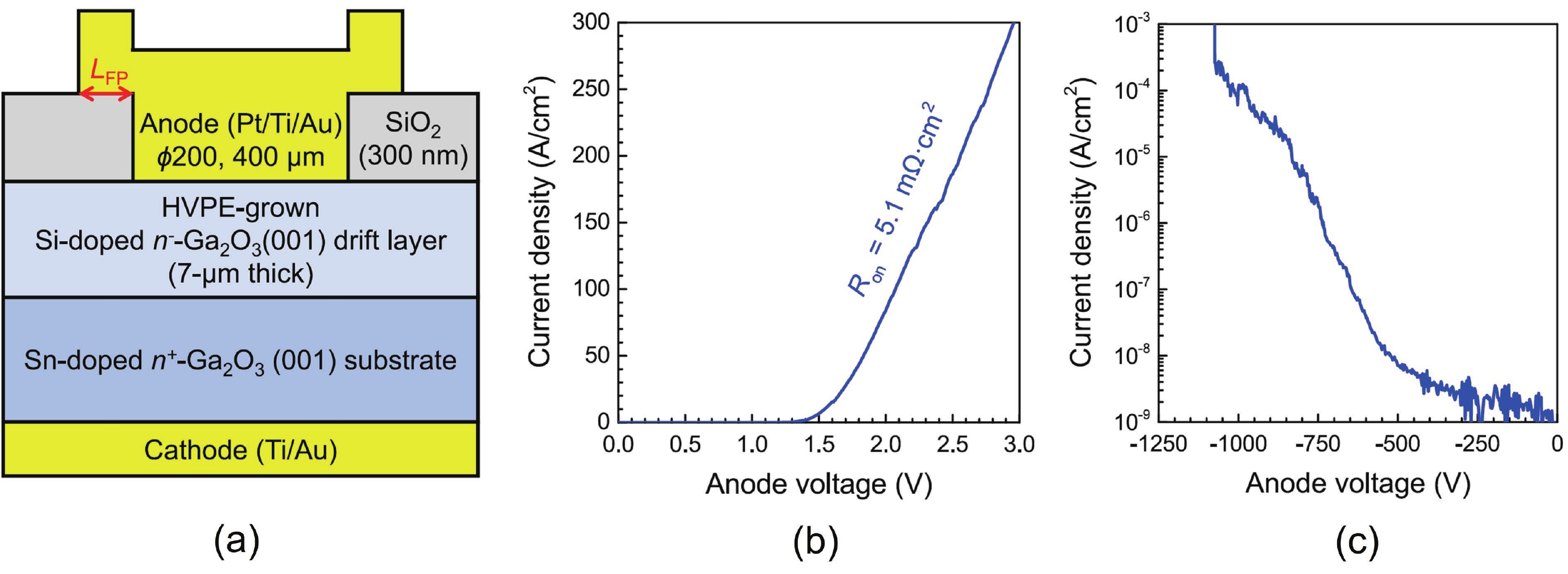
Konishi K, Goto K, Murakami H, et al. 1-kV vertical Ga 2O 3 field-plated Schottky barrier diodes. Appl Phys Lett, 2017, 110, 103506 doi: 10.1063/1.4977857 |
| [22] |
Hu Z Z, Zhou H, Feng Q, et al. Field-plated lateral β-Ga 2O 3 Schottky barrier diode with high reverse blocking voltage of more than 3 kV and high DC power figure-of-merit of 500 MW/cm 2. IEEE Electron Device Lett, 2018, 39, 1564 doi: 10.1109/LED.2018.2868444 |
| [23] |
Yang J C, Ren F, Tadjer M, et al. 2300V reverse breakdown voltage Ga 2O 3 Schottky rectifiers. ECS J Solid State Sci Technol, 2018, 7, Q92 doi: 10.1149/2.0241805jss |
| [24] |
Chen Y T, Yang J C, Ren F, et al. Implementation of a 900V switching circuit for high breakdown voltage β-Ga 2O 3 Schottky diodes. ECS J Solid State Sci Technol, 2019, 8, Q3229 doi: 10.1149/2.0421907jss |
| [25] |
Kumar S, Murakami H, Kumagai Y, et al. Vertical β-Ga 2O 3 Schottky barrier diodes with trench staircase field plate. Appl Phys Express, 2022, 15, 054001 doi: 10.35848/1882-0786/ac620b |
| [26] |
Yang J C, Ren F, Tadjer M, et al. Ga 2O 3 Schottky rectifiers with 1 ampere forward current, 650 V reverse breakdown and 26.5 MW•cm -2 figure-of-merit. AIP Adv, 2018, 8, 055026 doi: 10.1063/1.5034444 |
| [27] |
Yang J C, Ren F, Pearton S J, et al. Vertical geometry, 2-A forward current Ga 2O 3 Schottky rectifiers on bulk Ga 2O 3 substrates. IEEE Trans Electron Devices, 2018, 65, 2790 doi: 10.1109/TED.2018.2838439 |
| [28] |
Yang J C, Xian M H, Carey P, et al. Vertical geometry 33.2 A, 4.8 MW cm −2 Ga 2O 3 field-plated Schottky rectifier arrays. Appl Phys Lett, 2019, 114, 232106 doi: 10.1063/1.5100256 |
| [29] |
Yang J C, Fares C, Elhassani R, et al. Reverse breakdown in large area, field-plated, vertical β-Ga 2O 3 rectifiers. ECS J Solid State Sci Technol, 2019, 8, Q3159 doi: 10.1149/2.0211907jss |
| [30] |
Ji M, Taylor N R, Kravchenko I, et al. Demonstration of large-size vertical Ga 2O 3 Schottky barrier diodes. IEEE Trans Power Electron, 2020, 36, 41 doi: 10.1109/TPEL.2020.3001530 |
| [31] |
Sharma R, Xian M H, Fares C, et al. Effect of probe geometry during measurement of >100 A Ga 2O 3 vertical rectifiers. J Vac Sci Technol A, 2021, 39, 013406 doi: 10.1116/6.0000815 |
| [32] |
Kasu M, Hanada K, Moribayashi T, et al. Relationship between crystal defects and leakage current in β-Ga 2O 3 Schottky barrier diodes. Jpn J Appl Phys, 2016, 55, 1202BB doi: 10.7567/JJAP.55.1202BB |
| [33] |
Oshima T, Hashiguchi A, Moribayashi T, et al. Electrical properties of Schottky barrier diodes fabricated on (001) β-Ga 2O 3 substrates with crystal defects. Jpn J Appl Phys, 2017, 56, 086501 doi: 10.7567/JJAP.56.086501 |
| [34] |
Sdoeung S, Sasaki K, Kawasaki K, et al. Origin of reverse leakage current path in edge-defined film-fed growth (001) β-Ga 2O 3 Schottky barrier diodes observed by high-sensitive emission microscopy. Appl Phys Lett, 2020, 117, 022106 doi: 10.1063/5.0012794 |
| [35] |
Sdoeung S, Sasaki K, Kawasaki K, et al. Polycrystalline defects—Origin of leakage current—In halide vapor phase epitaxial (001) β-Ga 2O 3 Schottky barrier diodes identified via ultrahigh sensitive emission microscopy and synchrotron X-ray topography. Appl Phys Express, 2021, 14, 036502 doi: 10.35848/1882-0786/abde74 |
| [36] |
Xia Z B, Wang C Y, Kalarickal N K, et al. Design of transistors using high-permittivity materials. IEEE Trans Electron Devices, 2019, 66, 896 doi: 10.1109/TED.2018.2888834 |
| [37] |
Lee H-S, Kalarickal N K, Rahman M W, et al. High-permittivity dielectric edge termination for vertical high voltage devices. J Comput Electron, 2020, 19, 1538 doi: 10.1007/s10825-020-01553-y |
| [38] |
Kalarickal N K, Feng Z X, Bhuiyan A F M A U, et al. Electrostatic engineering using extreme permittivity materials for ultra-wide bandgap semiconductor transistors. IEEE Trans Electron Devices, 2021, 68, 29 doi: 10.1109/TED.2020.3037271 |
| [39] |
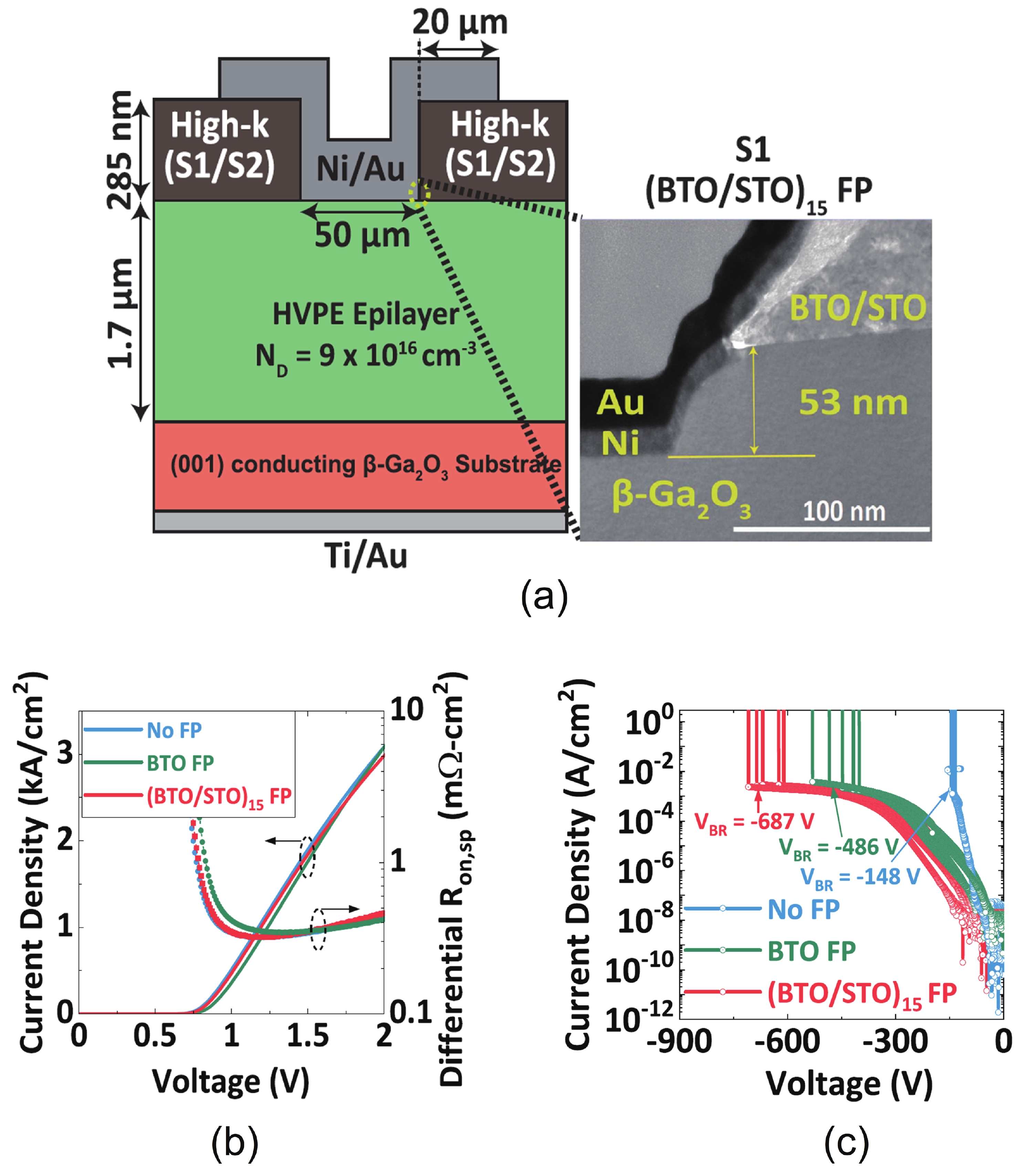
Xia Z B, Chandrasekar H, Moore W, et al. Metal/BaTiO 3/ β-Ga 2O 3 dielectric heterojunction diode with 5.7 MV/cm breakdown field. Appl Phys Lett, 2019, 115, 252104 doi: 10.1063/1.5130669 |
| [40] |
Roy S, Bhattacharyya A, Ranga P, et al. High-k oxide field-plated vertical (001) β-Ga 2O 3 Schottky barrier diode with baliga’s figure of merit over 1 GW/cm 2. IEEE Electron Device Lett, 2021, 42, 1140 doi: 10.1109/LED.2021.3089945 |
| [41] |
Saraswat D, Li W S, Nomoto K, et al. Very high parallel-plane surface electric field of 4.3 MV/cm in Ga 2O 3 Schottky barrier diodes with PtO x contacts. 2020 78th Device Research Conference (DRC), 2020, 1 doi: 10.1109/DRC50226.2020.9135177 |
| [42] |
Farzana E, Alema F, Ho W Y, et al. Vertical β-Ga 2O 3 field plate Schottky barrier diode from metal-organic chemical vapor deposition. Appl Phys Lett, 2021, 118, 162109 doi: 10.1063/5.0047821 |
| [43] |
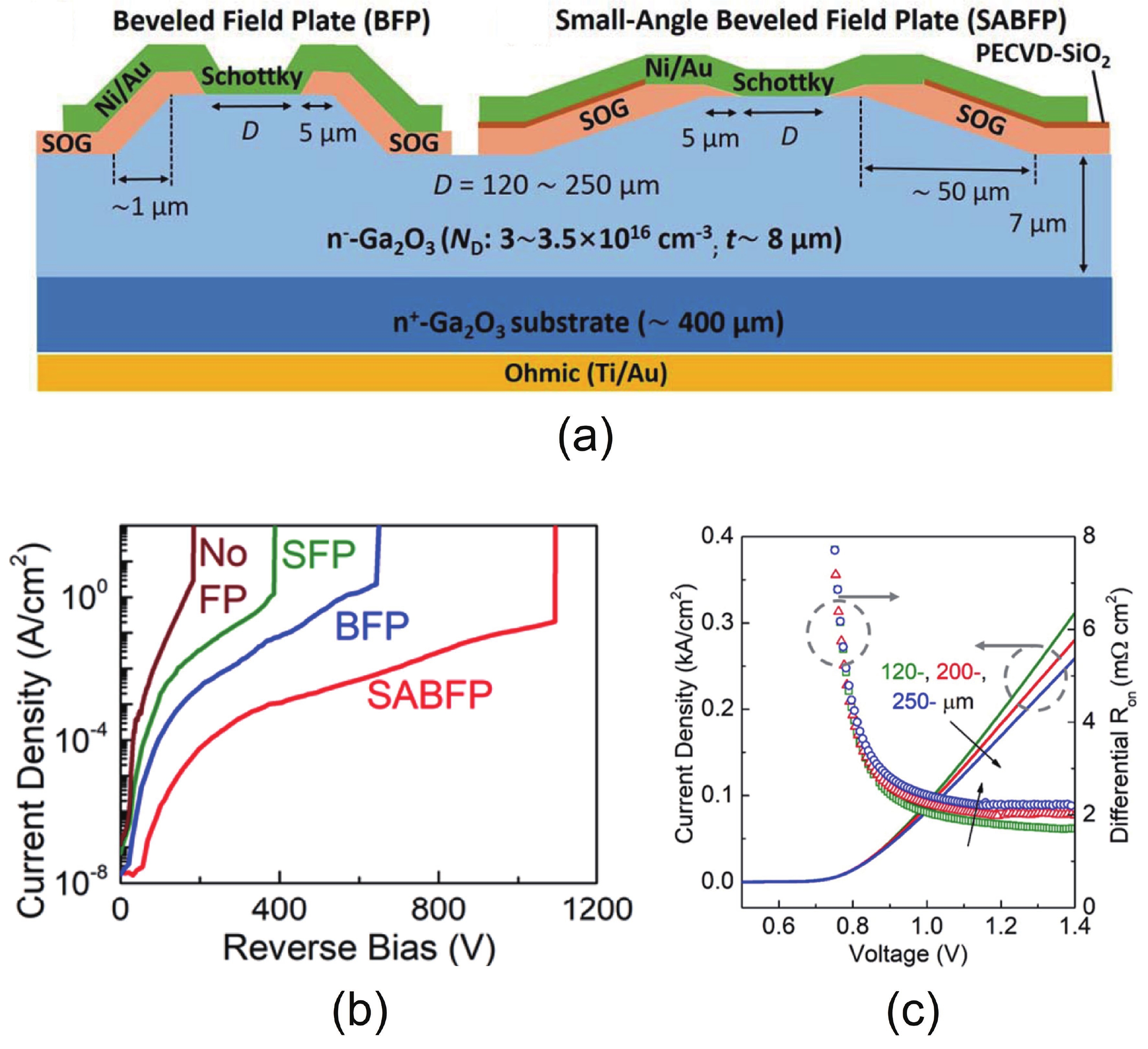
Joishi C, Rafique S, Xia Z B, et al. Low-pressure CVD-grown β-Ga 2O 3 bevel-field-plated Schottky barrier diodes. Appl Phys Express, 2018, 11, 031101 doi: 10.7567/APEX.11.031101 |
| [44] |
Allen N, Xiao M, Yan X D, et al. Vertical Ga 2O 3 Schottky barrier diodes with small-angle beveled field plates: A Baliga’s figure-of-merit of 0.6 GW/cm 2. IEEE Electron Device Lett, 2019, 40, 1399 doi: 10.1109/LED.2019.2931697 |
| [45] |
Zhang Y N, Zhang J C, Feng Z Q, et al. Impact of implanted edge termination on vertical β-Ga 2O 3 Schottky barrier diodes under OFF-state stressing. IEEE Trans Electron Devices, 2020, 67, 3948 doi: 10.1109/TED.2020.3002327 |
| [46] |
Lu X, Zhang X, Jiang H X, et al. Vertical β-Ga 2O 3 Schottky barrier diodes with enhanced breakdown voltage and high switching performance. Phys Status Solidi A, 2020, 217, 1900497 doi: 10.1002/pssa.201900497 |
| [47] |
Gao Y Y, Li A, Feng Q, et al. High-voltage β-Ga 2O 3 Schottky diode with argon-implanted edge termination. Nanoscale Res Lett, 2019, 14, 8 doi: 10.1186/s11671-018-2849-y |
| [48] |
Zhou H, Yan Q L, Zhang J C, et al. High-performance vertical β-Ga 2O 3 Schottky barrier diode with implanted edge termination. IEEE Electron Device Lett, 2019, 40, 1788 doi: 10.1109/LED.2019.2939788 |
| [49] |
Xia X Y, Xian M H, Fares C, et al. Nitrogen ion-implanted resistive regions for edge termination of vertical Ga 2O 3 rectifiers. J Vac Sci Technol A, 2021, 39, 063405 doi: 10.1116/6.0001347 |
| [50] |
Lin C-H, Yuda Y, Wong M H, et al. Vertical Ga 2O 3 Schottky barrier diodes with guard ring formed by nitrogen-ion implantation. IEEE Electron Device Lett, 2019, 40, 1487 doi: 10.1109/LED.2019.2927790 |
| [51] |
Dong P F, Zhang J C, Yan Q L, et al. 6 kV/3.4 mΩ·cm 2 vertical β-Ga 2O 3 Schottky barrier diode with BV 2/ Ron,sp performance exceeding 1-D unipolar limit of GaN and SiC. IEEE Electron Device Lett, 2022, 43, 765 doi: 10.1109/LED.2022.3160366 |
| [52] |
Oshima T, Kaminaga K, Mukai A, et al. Formation of semi-insulating layers on semiconducting β-Ga 2O 3 single crystals by thermal oxidation. Jpn J Appl Phys, 2013, 52, 051101 doi: 10.7567/JJAP.52.051101 |
| [53] |
Swain S K, Weber M H, Jesenovec J, et al. Compensation of shallow donors by gallium vacancies in monoclinic β-Ga 2O 3. Phys Rev Applied, 2021, 15, 054010 doi: 10.1103/PhysRevApplied.15.054010 |
| [54] |
Wang Y G, Lv Y J, Long S B, et al. High-voltage ( $\bar{{2}} 01 $) β-Ga 2O 3 vertical Schottky barrier diode with thermally-oxidized termination. IEEE Electron Device Lett, 2020, 41, 131 doi: 10.1109/LED.2019.2956016 |
| [55] |
Wang Y G, Lv Y J, Dun S B, et al. High performance β-Ga 2O 3 vertical Schottky barrier diodes. 2020 17th China International Forum on Solid State Lighting & 2020 6th International Forum on Wide Bandgap Semiconductors China, 2020, 224 doi: 10.1109/SSLChinaIFWS51786.2020.9308713 |
| [56] |
Wei Y X, Luo X R, Wang Y G, et al. Experimental study on static and dynamic characteristics of Ga 2O 3 Schottky barrier diodes with compound termination. IEEE Trans Power Electron, 2021, 36, 10976 doi: 10.1109/TPEL.2021.3069918 |
| [57] |
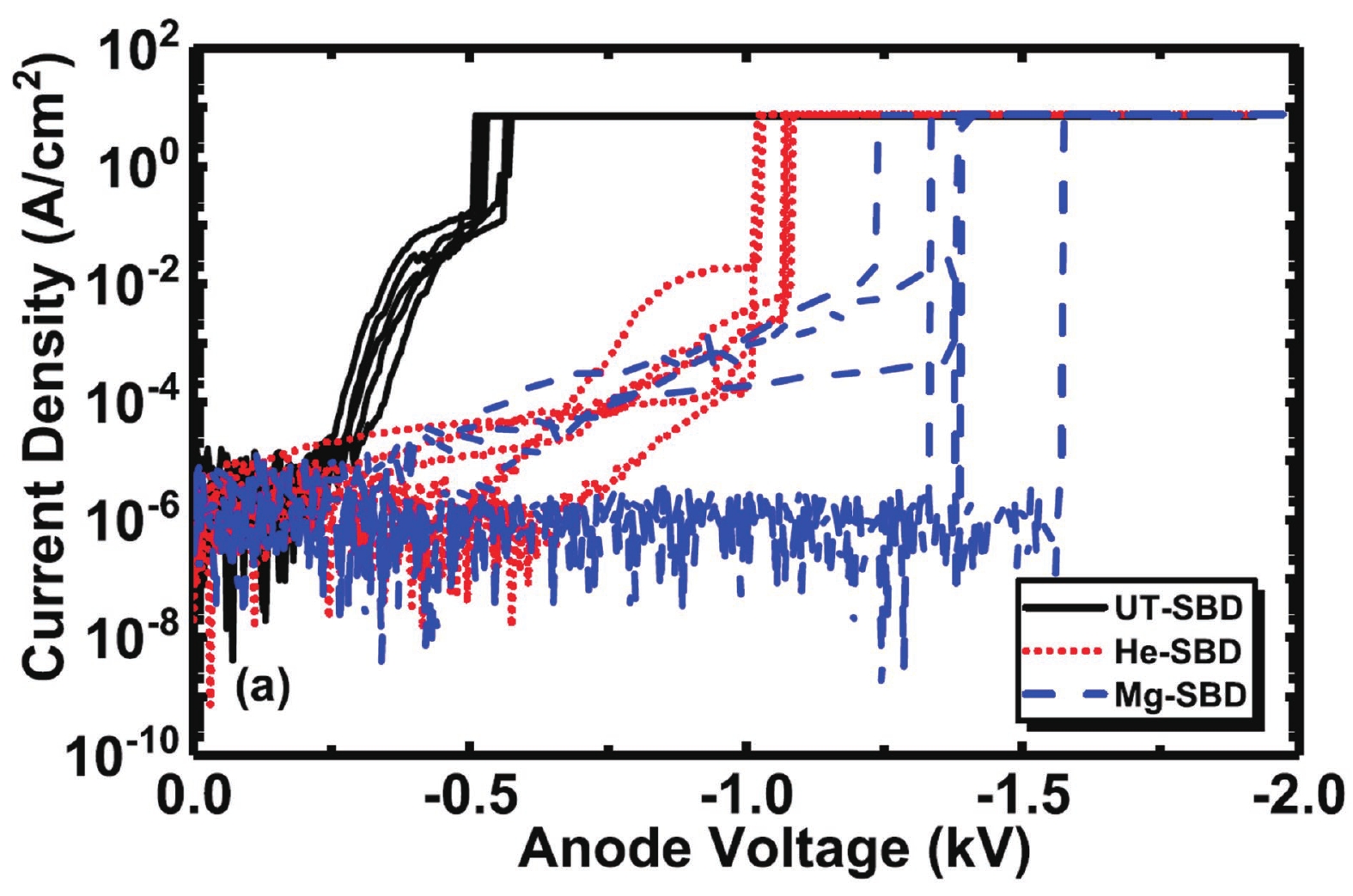
Hu Z Z, Lv Y J, Zhao C Y, et al. Beveled fluoride plasma treatment for vertical β-Ga 2O 3 Schottky barrier diode with high reverse blocking voltage and low turn-on voltage. IEEE Electron Device Lett, 2020, 41, 441 doi: 10.1109/LED.2020.2968587 |
| [58] |
Yang J C, Fares C, Ren F, et al. Effects of fluorine incorporation into β-Ga 2O 3. J Appl Phys, 2018, 123, 441 doi: 10.1063/1.5031001 |
| [59] |
Yan Q L, Gong H H, Zhou H, et al. Low density of interface trap states and temperature dependence study of Ga 2O 3 Schottky barrier diode with p-NiO x termination. Appl Phys Lett, 2022, 120, 092106 doi: 10.1063/5.0082377 |
| [60] |
Roy S, Bhattacharyya A, Krishnamoorthy S. Design of a β-Ga 2O 3 Schottky barrier diode with p-type III-nitride guard ring for enhanced breakdown. IEEE Trans Electron Devices, 2020, 67, 4842 doi: 10.1109/TED.2020.3025268 |
| [61] |
Wang B Y, Xiao M, Spencer J, et al. 2.5 kV vertical Ga 2O 3 Schottky rectifier with graded junction termination extension. IEEE Electron Device Lett, 2023, 44, 221 doi: 10.1109/LED.2022.3229222 |
| [62] |
Hao W B, Wu F H, Li W S, et al. Improved vertical β-Ga 2O 3 Schottky barrier diodes with conductivity-modulated p-NiO junction termination extension. IEEE Trans Electron Devices, 2023, 70, 2129 doi: 10.1109/TED.2023.3241885 |
| [63] |
Gong H H, Yu X X, Xu Y, et al. β-Ga 2O 3 vertical heterojunction barrier Schottky diodes terminated with p-NiO field limiting rings. Appl Phys Lett, 2021, 118, 202102 doi: 10.1063/5.0050919 |
| [64] |
Hu Z, Zhao C, Feng Q, et al. The investigation of β-Ga 2O 3 Schottky diode with floating field ring termination and the interface states. ECS J Solid State Sci Technol, 2020, 9(2), 025001 doi: 10.1149/2162-8777/ab6162 |
| [65] |
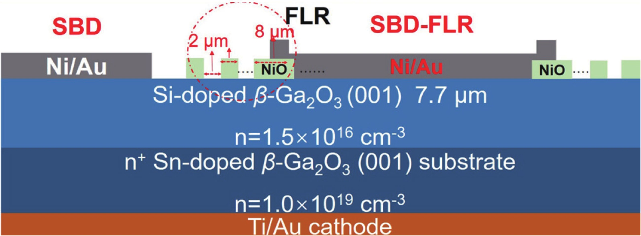
Sharma R, Xian M H, Law M E, et al. Design and implementation of floating field ring edge termination on vertical geometry β-Ga 2O 3 rectifiers. J Vac Sci Technol A, 2020, 38, 063414 doi: 10.1116/6.0000693 |
| [66] |
|
| [67] |
Li W S, Saraswat D, Long Y Y, et al. Near-ideal reverse leakage current and practical maximum electric field in β-Ga 2O 3 Schottky barrier diodes. Appl Phys Lett, 2020, 116, 192101 doi: 10.1063/5.0007715 |
| [68] |
|
| [69] |
Baliga B J. The pinch rectifier: A low-forward-drop high-speed power diode. IEEE Electron Device Lett, 1984, 5, 194 doi: 10.1109/EDL.1984.25884 |
| [70] |
Baliga B J. Analysis of a high-voltage merged p-i-n/Schottky (MPS) rectifier. IEEE Electron Device Lett, 1987, 8, 407 doi: 10.1109/EDL.1987.26676 |
| [71] |
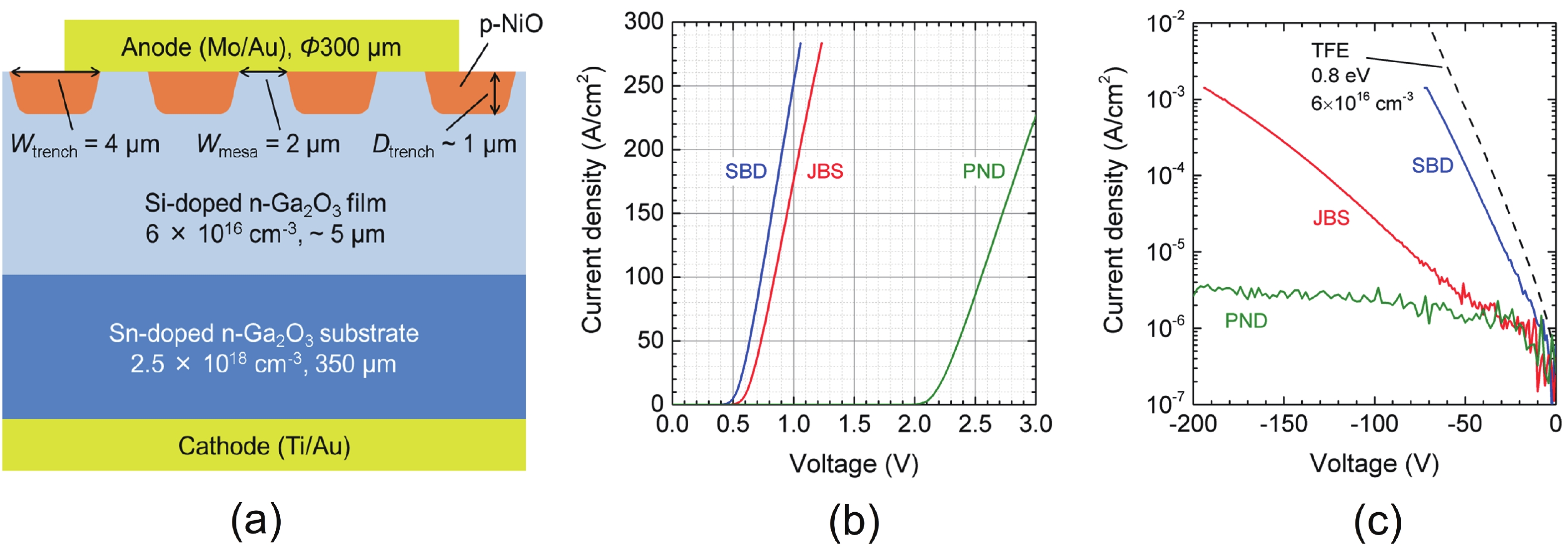
Sasaki K, Thieu Q T, Wakimoto D, et al. First demonstration of Ga2O3 junction barrier Schottky diodes. 2017 17th International Conference on Silicon Carbide and Related Materials (ICSCRM), 2017, WE.E1.7
|
| [72] |
Sasaki K, Yamakoshi S, Kuramata A. Gallium-oxide trench-type devices. Proc SPIE, 2019, 10919, 1091913 doi: 10.1117/12.2515491 |
| [73] |
Yan Q L, Gong H H, Zhang J C, et al. β-Ga 2O 3 hetero-junction barrier Schottky diode with reverse leakage current modulation and BV 2/ Ron,sp value of 0.93 GW/cm 2. Appl Phys Lett, 2021, 118, 122102 doi: 10.1063/5.0044130 |
| [74] |
Lv Y J, Wang Y G, Fu X C, et al. Demonstration of β-Ga 2O 3 junction barrier Schottky diodes with a Baliga’s figure of merit of 0.85 GW/cm 2 or a 5A/700 V handling capabilities. IEEE Trans Power Electron, 2021, 36, 6179 doi: 10.1109/TPEL.2020.3036442 |
| [75] |
Sasaki K, Wakimoto D, Thieu Q T, et al. First demonstration of Ga 2O 3 trench MOS-type Schottky barrier diodes. IEEE Electron Device Lett, 2017, 38, 783 doi: 10.1109/LED.2017.2696986 |
| [76] |
Takatsuka A, Sasaki K, Wakimoto D, et al. Fast recovery performance of β-Ga 2O 3 trench MOS Schottky barrier diodes. 2018 76th Device Research Conference (DRC), 2018, 1 doi: 10.1109/DRC.2018.8442267 |
| [77] |
Otsuka F, Miyamoto H, Takatsuka A, et al. Large-size (1.7 × 1.7 mm 2 β-Ga 2O 3 field-plated trench MOS-type Schottky barrier diodes with 1.2 kV breakdown voltage and 10 9 high on/off current ratio. Appl Phys Express, 2022, 15, 016501 doi: 10.35848/1882-0786/ac4080 |
| [78] |
Li W S, Nomoto K, Hu Z Y, et al. 1.5 kV vertical Ga 2O 3 trench-MIS Schottky barrier diodes. 2018 76th Device Research Conference (DRC), 2018, 1 doi: 10.1109/DRC.2018.8442245 |
| [79] |
Li W S, Hu Z Y, Nomoto K, et al. 1230 V β-Ga 2O 3 trench Schottky barrier diodes with an ultra-low leakage current of 1 μA/cm 2. Appl Phys Lett, 2018, 113, 202101 doi: 10.1063/1.5052368 |
| [80] |
Li W S, Hu Z Y, Nomoto K, et al. 2.44 kV Ga 2O 3 vertical trench Schottky barrier diodes with very low reverse leakage current. 2018 IEEE International Electron Devices Meeting (IEDM), 2018, 8.5. 1 doi: 10.1109/IEDM.2018.8614693 |
| [81] |
Li W S, Nomoto K, Hu Z Y, et al. Field-plated Ga 2O 3 trench Schottky barrier diodes with a record high figure-of-merit of 0.78 GW/cm 2. 2019 77th Device Research Conference (DRC), 2019, 1 doi: 10.1109/DRC46940.2019.9046425 |
| [82] |
Li W S, Nomoto K, Hu Z Y, et al. Field-plated Ga 2O 3 trench Schottky barrier diodes with a BV 2/ Ron,sp of up to 0.95 GW/cm 2. IEEE Electron Device Lett, 2020, 41, 107 doi: 10.1109/LED.2019.2953559 |
| [83] |
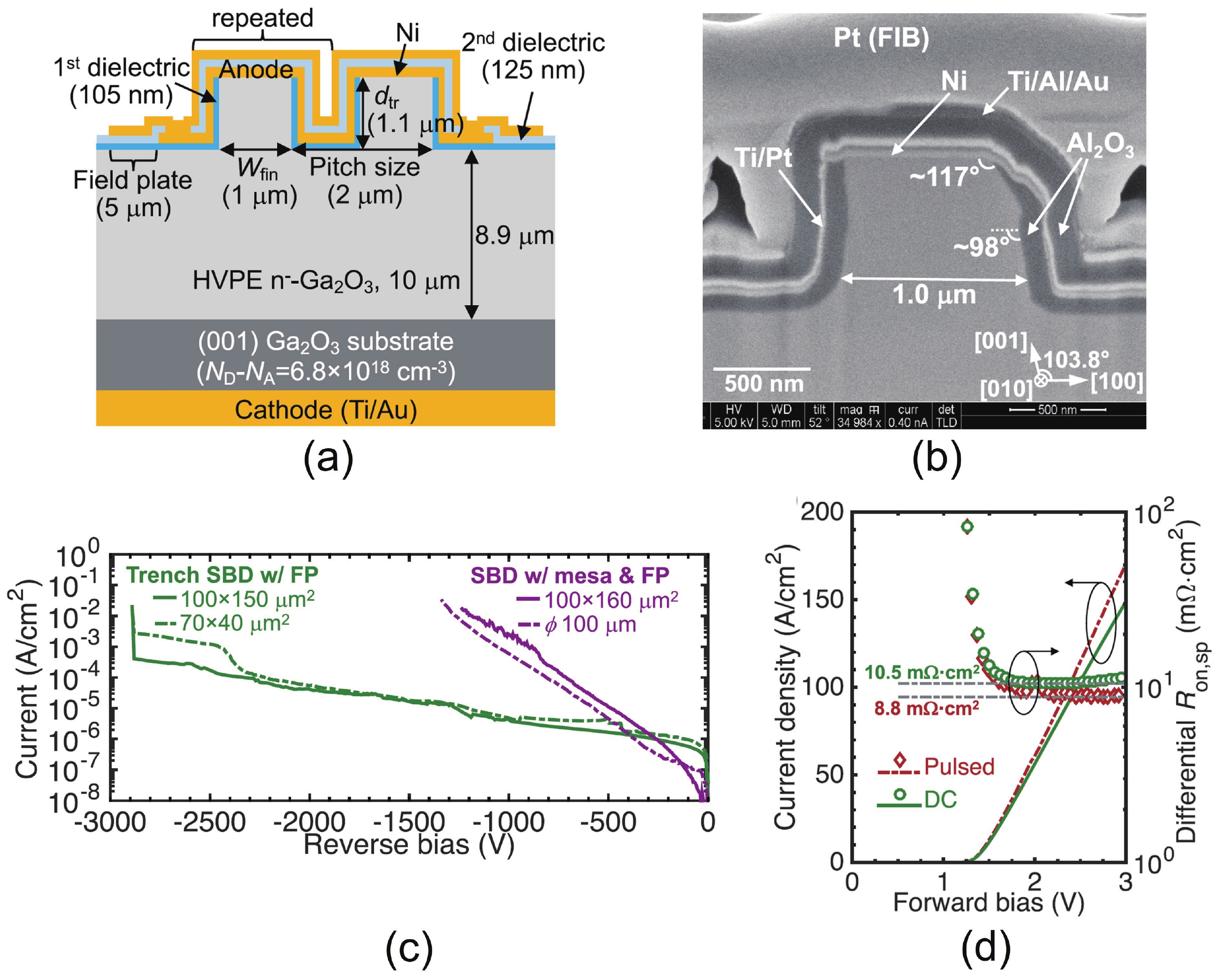
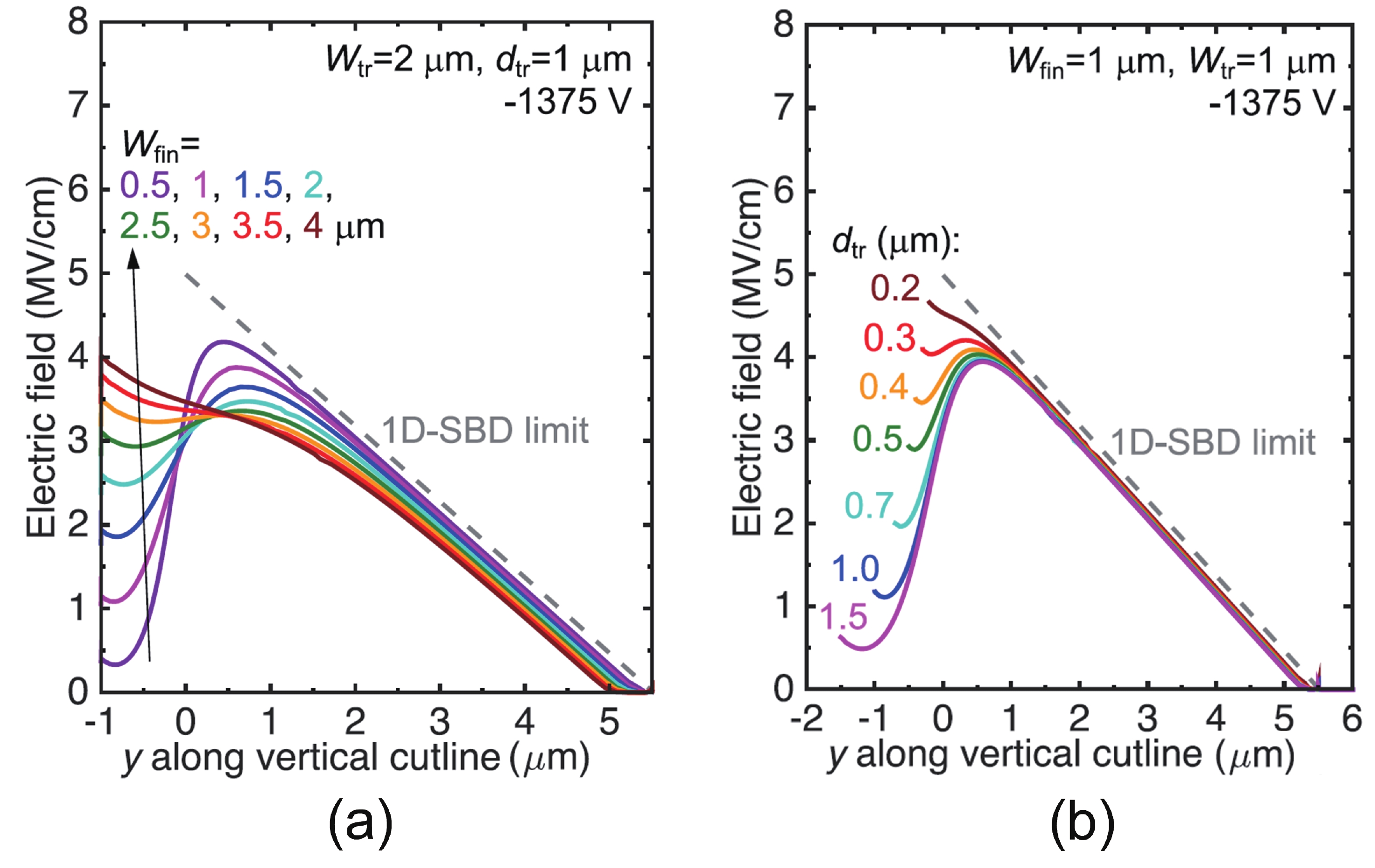
Li W S, Nomoto K, Hu Z Y, et al. Guiding principles for trench Schottky barrier diodes based on ultrawide bandgap semiconductors: A case study in Ga 2O 3. IEEE Trans Electron Devices, 2020, 67, 3938 doi: 10.1109/TED.2020.3003292 |
| [84] |
Huang X A, Liao F, Li L, et al. 3.4 kV breakdown voltage Ga 2O 3 trench Schottky diode with optimized trench corner radius. ECS J Solid State Sci Technol, 2020, 9, 045012 doi: 10.1149/2162-8777/ab8b4a |
| [85] |
Li W S, Nomoto K, Hu Z Y, et al. Fin-channel orientation dependence of forward conduction in kV-class Ga 2O 3 trench Schottky barrier diodes. Appl Phys Express, 2019, 12, 061007 doi: 10.7567/1882-0786/ab206c |
| [86] |
Li W S, Nomoto K, Hu Z Y, et al. ON-resistance of Ga 2O 3 trench-MOS Schottky barrier diodes: Role of sidewall interface trapping. IEEE Trans Electron Devices, 2021, 68, 2420 doi: 10.1109/TED.2021.3067856 |
| [87] |
Fares C, Ren F, Pearton S J. Temperature-dependent electrical characteristics of β-Ga 2O 3 diodes with W Schottky contacts up to 500 °C. ECS J Solid State Sci Technol, 2018, 8, Q3007 doi: 10.1149/2.0011907jss |
| [88] |
Hou C, York K R, Makin R A, et al. High temperature (500 °C) operating limits of oxidized platinum group metal (PtO x, IrO x, PdO x, RuO x) Schottky contacts on β-Ga 2O 3. Appl Phys Lett, 2020, 117, 203502 doi: 10.1063/5.0026345 |
| [89] |
Gong H H, Zhou F, Yu X X, et al. 70- μm-body Ga 2O 3 Schottky barrier diode with 1.48 K/W thermal resistance, 59 A surge current and 98.9% conversion efficiency. IEEE Electron Device Lett, 2022, 43, 773 doi: 10.1109/LED.2022.3162393 |
| [90] |
Xiao M, Wang B Y, Liu J C, et al. Packaged Ga 2O 3 Schottky rectifiers with over 60-A surge current capability. IEEE Trans Power Electron, 2021, 36, 8565 doi: 10.1109/TPEL.2021.3049966 |
| [91] |
Buttay C, Wong H Y, Wang B Y, et al. Surge current capability of ultra-wide-bandgap Ga 2O 3 Schottky diodes. Microelectron Reliab, 2020, 114, 113743 doi: 10.1016/j.microrel.2020.113743 |
| [92] |
Jian Z A, Mohanty S, Ahmadi E. Temperature-dependent current-voltage characteristics of β-Ga 2O 3 trench Schottky barrier diodes. Appl Phys Lett, 2020, 116, 152104 doi: 10.1063/5.0002520 |
| [93] |
Wilhelmi F, Kunori S, Sasaki K, et al. Packaged β-Ga 2O 3 trench MOS Schottky diode with nearly ideal junction properties. IEEE Trans Power Electron, 2022, 37, 3737 doi: 10.1109/TPEL.2021.3122902 |
| [94] |
Neal A T, Mou S, Lopez R, et al. Incomplete ionization of a 110 meV unintentional donor in β-Ga 2O 3 and its effect on power devices. Sci Rep, 2017, 7, 13218 doi: 10.1038/s41598-017-13656-x |
| [95] |
Zhou F, Gong H H, Xiao M, et al. An avalanche-and-surge robust ultrawide-bandgap heterojunction for power electronics. Nat Commun, 2023, 14, 4459 doi: 10.1038/s41467-023-40194-0 |
| [96] |
Wang C L, Gong H H, Lei W N, et al. Demonstration of the p-NiO x/n-Ga 2O 3 heterojunction gate FETs and diodes with BV 2/ Ron,sp figures of merit of 0.39 GW/cm 2 and 1.38 GW/cm 2. IEEE Electron Device Lett, 2021, 42, 485 doi: 10.1109/LED.2021.3062851 |
| [97] |
Zhou F, Gong H H, Wang Z P, et al. Over 1.8 GW/cm 2 beveled-mesa NiO/ β-Ga 2O 3 heterojunction diode with 800 V/10 A nanosecond switching capability. Appl Phys Lett, 2021, 119, 262103 doi: 10.1063/5.0071280 |
| [98] |
Hao W B, He Q M, Zhou X Z, et al. 2.6 kV NiO/Ga 2O 3 heterojunction diode with superior high-temperature voltage blocking capability. 2022 IEEE 34th International Symposium on Power Semiconductor Devices and ICs (ISPSD), 2022, 105 doi: 10.1109/ISPSD49238.2022.9813680 |
| [99] |
Zhang J C, Dong P F, Dang K, et al. Ultra-wide bandgap semiconductor Ga 2O 3 power diodes. Nat Commun, 2022, 13, 3900 doi: 10.1038/s41467-022-31664-y |
| [100] |
Xiao M, Wang B Y, Spencer J, et al. NiO junction termination extension for high-voltage ( > 3 kV) Ga 2O 3 devices. Appl Phys Lett, 2023, 122, 183501 doi: 10.1063/5.0142229 |


 DownLoad:


 Man Hoi Wong:is an Associate Professor at the Department of Electronic and Computer Engineering at the Hong Kong University of Science and Technology (HKUST). He received his Ph.D. from the University of California Santa Barbara, USA, in 2009. Prof. Wong has worked at the SEMATECH corporate research consortium in the USA and the National Institute of Information and Communications Technology in Japan as a research scientist. Prior to joining HKUST, he was an Assistant Professor at the University of Massachusetts Lowell, USA. His current research focuses on ultrawide-bandgap semiconductor materials and power devices


