


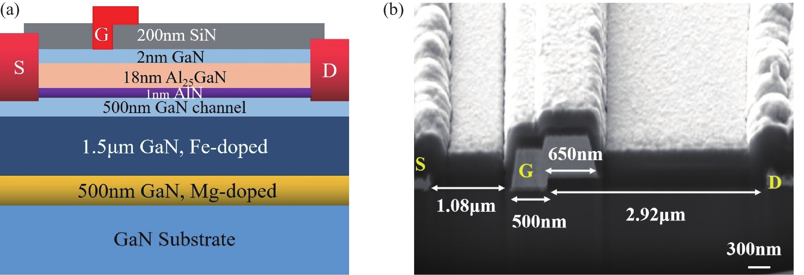
Fig. 1.
(Color online) (a) Schematic cross-section of the AlGaN/GaN HEMT on a GaN substrate and (b) the SEM image of the Γ-shaped gate.
ARTICLES
Yansheng Hu§, Yuangang Wang§, Wei Wang, Yuanjie Lv, Hongyu Guo, Zhirong Zhang, Hao Yu, Xubo Song, Xingye zhou, Tingting Han, Shaobo Dun, Hongyu Liu, Aimin Bu and Zhihong Feng
Corresponding author: Yuanjie Lv, yuanjielv@163.com; Zhihong Feng, ga917vv@163.com
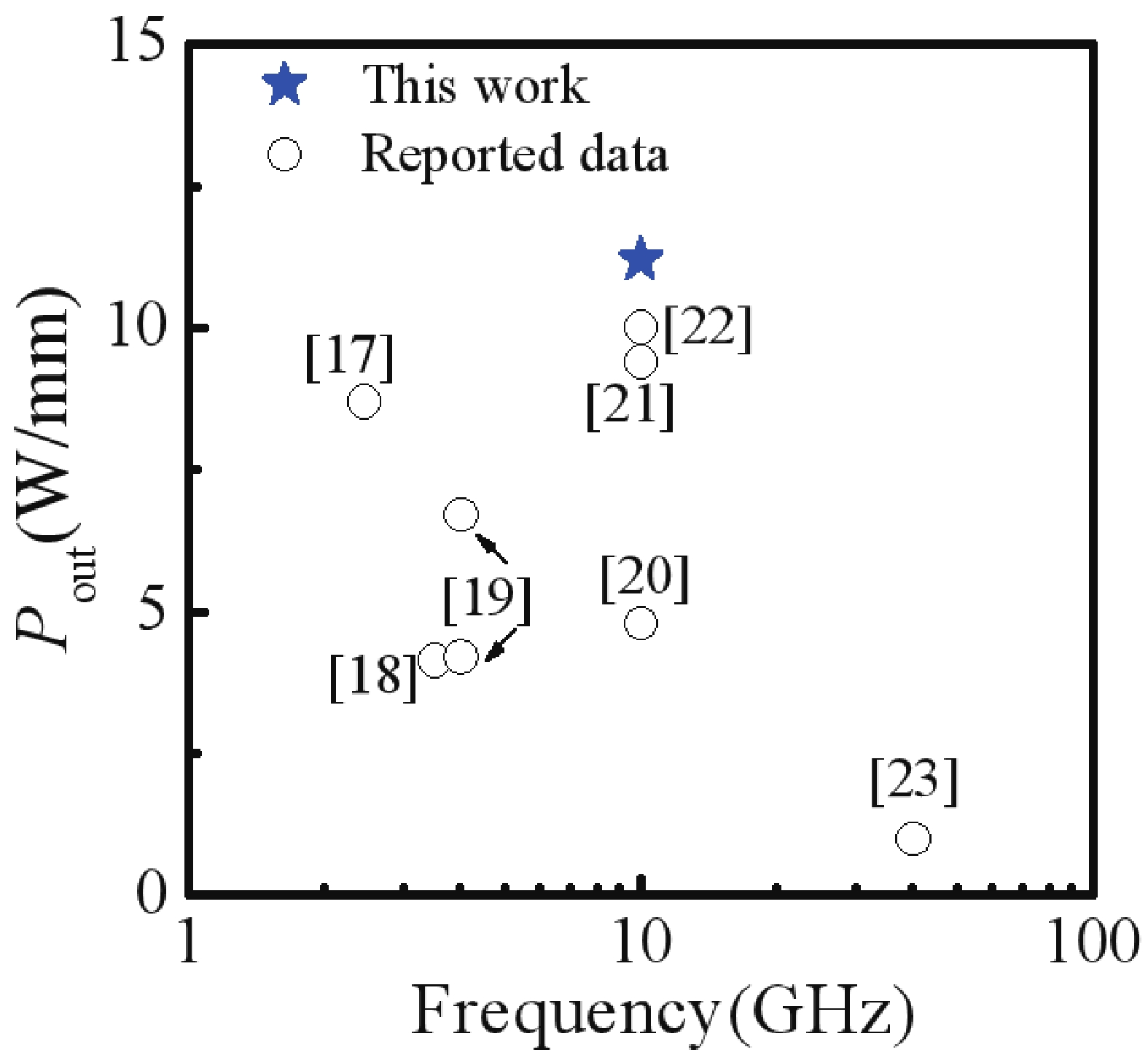
Abstract: In this letter, high power density AlGaN/GaN high electron-mobility transistors (HEMTs) on a freestanding GaN substrate are reported. An asymmetric Γ-shaped 500-nm gate with a field plate of 650 nm is introduced to improve microwave power performance. The breakdown voltage (BV) is increased to more than 200 V for the fabricated device with gate-to-source and gate-to-drain distances of 1.08 and 2.92 μm. A record continuous-wave power density of 11.2 W/mm@10 GHz is realized with a drain bias of 70 V. The maximum oscillation frequency (fmax) and unity current gain cut-off frequency (ft) of the AlGaN/GaN HEMTs exceed 30 and 20 GHz, respectively. The results demonstrate the potential of AlGaN/GaN HEMTs on free-standing GaN substrates for microwave power applications.
Keywords: freestanding GaN substrates, AlGaN/GaN HEMTs, continuous-wave power density, breakdown voltage, Γ-shaped gate
| [1] |
Wu Y F, Moore M, Saxler A, et al. 40-W/mm double field-plated GaN HEMTs. 2006 64th Device Research Conference, 2006, 151 doi: 10.1109/DRC.2006.305162
|
| [2] |
Tilak V, Green B, Kaper V, et al. Influence of barrier thickness on the high-power performance of AlGaN/GaN HEMTs. IEEE Electron Device Lett, 2001, 22, 504 doi: 10.1109/55.962644
|
| [3] |
Yue Y Z, Hu Z Y, Guo J, et al. Ultrascaled InAlN/GaN high electron mobility transistors with cutoff frequency of 400 GHz. Jpn J Appl Phys, 2013, 52, 08JN14 doi: 10.7567/JJAP.52.08JN14
|
| [4] |
Palacios T, Chakraborty A, Rajan S, et al. High-power AlGaN/GaN HEMTs for ka-band applications. IEEE Electron Device Lett, 2005, 26, 781 doi: 10.1109/LED.2005.857701
|
| [5] |
Koehler A D, Anderson T J, Hite J K, et al. Degradation mechanisms of AlGaN/GaN HEMTs on sapphire, Si, and SiC substrates under Proton. 2014 IEEE Workshop on Wide Bandgap Power Devices and Applications, 2014, 33 doi: 10.1109/WiPDA.2014.6964619
|
| [6] |
Hsu J W P, Manfra M J, Molnar R J, et al. Direct imaging of reverse-bias leakage through pure screw dislocations in GaN films grown by molecular beam epitaxy on GaN templates. Appl Phys Lett, 2002, 81, 79 doi: 10.1063/1.1490147
|
| [7] |
Hsu C Y, Lan W H, Wu Y S. Effect of thermal annealing of Ni/Au ohmic contact on the leakage current of GaN based light emitting diodes. Appl Phys Lett, 2003, 83, 2447 doi: 10.1063/1.1601306
|
| [8] |
Nakamura S. III-V nitride-based blue LDs with modulation-doped strained-layer superlattices. Compound Semiconductors 1997. Proceedings of the IEEE Twenty-Fourth International Symposium on Compound Semiconductors, 2002, 1 doi: 10.1109/ISCS.1998.711529
|
| [9] |
Anderson T J, Tadjer M J, Hite J K, et al. Effect of reduced extended defect density in MOCVD grown AlGaN/GaN HEMTs on native GaN substrates. IEEE Electron Device Lett, 2015, 37, 28 doi: 10.1109/LED.2015.2502221
|
| [10] |
Liu J P, Ryou J H, Yoo D, et al. III-nitride heterostructure field-effect transistors grown on semi-insulating GaN substrate without regrowth interface charge. Appl Phys Lett, 2008, 92, 133513 doi: 10.1063/1.2906372
|
| [11] |
Wu M, Leach J H, Ni X, et al. InAlN/GaN heterostructure field-effect transistors on Fe-doped semi-insulating GaN substrates. J Vac Sci Technol B Nanotechnol Microelectron Mater Process Meas Phenom, 2010, 28, 908 doi: 10.1116/1.3481138
|
| [12] |
Jana D, Chatterjee A, Sharma T K. Confirmation of the compensation of unintentional donors in AlGaN/GaN HEMT structures by Mg-doping during initial growth of GaN buffer layer. J Lumin, 2020, 219, 116904 doi: 10.1016/j.jlumin.2019.116904
|
| [13] |
Deen D A, Storm D F, Meyer D J, et al. Impact of barrier thickness on transistor performance in AlN/GaN high electron mobility transistors grown on free-standing GaN substrates. Appl Phys Lett, 2014, 105, 093503 doi: 10.1063/1.4895105
|
| [14] |
Kaun S W, Wong M H, Lu J, et al. Reduction of carbon proximity effects by including AlGaN back barriers in HEMTs on free-standing GaN. Electron Lett, 2013, 49, 893 doi: 10.1049/el.2013.1723
|
| [15] |
Tanabe S, Watanabe N, Matsuzaki H. Breakdown mechanism in AlGaN/GaN high-electron mobility transistor structure on free-standing n-type GaN substrate. Jpn J Appl Phys, 2016, 55, 05FK01 doi: 10.7567/JJAP.55.05FK01
|
| [16] |
Zhu M D, Song B, Hu Z Y, et al. Comparing buffer leakage in PolarMOSH on SiC and free-standing GaN substrates. 2016 Lester Eastman Conference (LEC), 2016, 27 doi: 10.1109/LEC.2016.7578926
|
| [17] |
Kumazaki Y, Ohki T, Kotani J, et al. Over 80% power-added-efficiency GaN high-electron-mobility transistors on free-standing GaN substrates. Appl Phys Express, 2021, 14, 016502 doi: 10.35848/1882-0786/abc1cc
|
| [18] |
Góralczyk M, Gryglewski D. S-band GaN PolHEMT power amplifier. 2016 21st International Conference on Microwave, Radar and Wireless Communications (MIKON), 2016, 1 doi: 10.1109/MIKON.2016.7492073
|
| [19] |
Storm D F, Katzer D S, Roussos J A, et al. AlGaN/GaN HEMTs on free-standing GaN substrates: MBE growth and microwave characterization. J Cryst Growth, 2007, 301/302, 429 doi: 10.1016/j.jcrysgro.2006.11.085
|
| [20] |
Chu K K, Chao P C, Pizzella M T, et al. 9.4-W/mm power density AlGaN–GaN HEMTs on free-standing GaN substrates. IEEE Electron Device Lett, 2004, 25, 596 doi: 10.1109/LED.2004.833847
|
| [21] |
Chu K K, Chao P C, Windyka J A. Stable high power GaN-on-GaN hemt. Int J Hi Spe Ele Syst, 2004, 14, 738 doi: 10.1142/S0129156404002764
|
| [22] |
Meyer D J, Deen D A, Storm D F, et al. High electron velocity submicrometer AlN/GaN MOS-HEMTs on freestanding GaN substrates. IEEE Electron Device Lett, 2013, 34, 199 doi: 10.1109/LED.2012.2228463
|
| [23] |
Wojtasiak W, Góralczyk M, Gryglewski D, et al. Micromachines, 2018, 9, 546
|
| [24] |
Asif Khan M, Yang J W, Knap W, et al. GaN–AlGaN heterostructure field-effect transistors over bulk GaN substrates. Appl Phys Lett, 2000, 76, 3807 doi: 10.1063/1.126788
|
| [25] |
Zhang Z R, Fang Y L, Yin J Y, et al. Highmobility AlGaN/GaN high electronic mobility transistors on GaN homo-substrates. Acta Phys Sin, 2018, 67, 076801 doi: 10.7498/aps.67.20172581
|
| [26] |
Ma T, Hao Y, Chen C, et al. A new small-signal model for asymmetrical AlGaN/GaN HEMTs. J Semicond, 2010, 31, 064002 doi: 10.1088/1674-4926/31/6/064002
|
| [27] |
Kumar V, Chen G, Guo S P, et al. Field-plated 0.25-μm gate-length AlGaN/GaN HEMTs with varying field-plate length. IEEE Trans Electron Devices, 2006, 53, 1477 doi: 10.1109/TED.2006.874090
|
| [28] |
Buttari D, Chini A, Meneghesso G, et al. Systematic characterization of Cl2 reactive ion etching for improved ohmics in AlGaN/GaN HEMTs. IEEE Electron Device Lett, 2002, 23, 76 doi: 10.1109/55.981311
|
| [29] |
Wang C, Cho S J, Kim N Y. Optimization of ohmic contact metallization process for AlGaN/GaN high electron mobility transistor. Trans Electr Electron Mater, 2013, 14, 32 doi: 10.4313/TEEM.2013.14.1.32
|
| [30] |
Bahat-Treidel E, Hilt O, Brunner F, et al. AlGaN/GaN/AlGaN DH-HEMTs breakdown voltage enhancement using multiple grating field plates (MGFPs). IEEE Trans Electron Devices, 2010, 57, 1208 doi: 10.1109/TED.2010.2045705
|
| [31] |
Wang C, Maharjan R K, Cho S J, et al. A novel manufacturing process of AlGaN/GaN HEMT for X-band high-power application on Si (111) substrate. 2012 Asia Pacific Microwave Conference Proceedings. Kaohsiung, Taiwan, China, 2013, 484 doi: 10.1109/APMC.2012.6421638
|
| [32] |
Chen Y C, Sanyal I, Hu T Y, et al. The influence of superlattice structure on the dynamic buffer response of AlInN/GaN-on-Si HEMTs. IEEE Trans Nanotechnol, 2020, 19, 415 doi: 10.1109/TNANO.2020.2992312
|


Article views: 3081 Times PDF downloads: 254 Times Cited by: 0 Times
Received: 28 July 2023 Revised: 04 September 2023 Online: Accepted Manuscript: 08 November 2023Corrected proof: 08 November 2023Uncorrected proof: 08 November 2023Published: 10 January 2024
| Citation: |
Yansheng Hu, Yuangang Wang, Wei Wang, Yuanjie Lv, Hongyu Guo, Zhirong Zhang, Hao Yu, Xubo Song, Xingye zhou, Tingting Han, Shaobo Dun, Hongyu Liu, Aimin Bu, Zhihong Feng. 11.2 W/mm power density AlGaN/GaN high electron-mobility transistors on a GaN substrate[J]. Journal of Semiconductors, 2024, 45(1): 012501. doi: 10.1088/1674-4926/45/1/012501
****
Y S Hu, Y G Wang, W Wang, Y J Lv, H Y Guo, Z R Zhang, H Yu, X B Song, X Y zhou, T T Han, S B Dun, H Y Liu, A M Bu, Z H Feng. 11.2 W/mm power density AlGaN/GaN high electron-mobility transistors on a GaN substrate[J]. J. Semicond, 2024, 45(1): 012501. doi: 10.1088/1674-4926/45/1/012501

|
 Yansheng Hu received his master's degree in radio physics from Lanzhou University in 2010. His research focuses on wide-gap semiconductor electronic devices
 Yuanjie Lv born in Tai'an City, Shandong Province, in 1985, is a professor who got a doctor's degree in microelectronics and solid-state electronics from Shandong University in 2012, mainly working in the research of wide-gap semiconductor electronic devices
| [1] |
Wu Y F, Moore M, Saxler A, et al. 40-W/mm double field-plated GaN HEMTs. 2006 64th Device Research Conference, 2006, 151 doi: 10.1109/DRC.2006.305162
|
| [2] |
Tilak V, Green B, Kaper V, et al. Influence of barrier thickness on the high-power performance of AlGaN/GaN HEMTs. IEEE Electron Device Lett, 2001, 22, 504 doi: 10.1109/55.962644
|
| [3] |
Yue Y Z, Hu Z Y, Guo J, et al. Ultrascaled InAlN/GaN high electron mobility transistors with cutoff frequency of 400 GHz. Jpn J Appl Phys, 2013, 52, 08JN14 doi: 10.7567/JJAP.52.08JN14
|
| [4] |
Palacios T, Chakraborty A, Rajan S, et al. High-power AlGaN/GaN HEMTs for ka-band applications. IEEE Electron Device Lett, 2005, 26, 781 doi: 10.1109/LED.2005.857701
|
| [5] |
Koehler A D, Anderson T J, Hite J K, et al. Degradation mechanisms of AlGaN/GaN HEMTs on sapphire, Si, and SiC substrates under Proton. 2014 IEEE Workshop on Wide Bandgap Power Devices and Applications, 2014, 33 doi: 10.1109/WiPDA.2014.6964619
|
| [6] |
Hsu J W P, Manfra M J, Molnar R J, et al. Direct imaging of reverse-bias leakage through pure screw dislocations in GaN films grown by molecular beam epitaxy on GaN templates. Appl Phys Lett, 2002, 81, 79 doi: 10.1063/1.1490147
|
| [7] |
Hsu C Y, Lan W H, Wu Y S. Effect of thermal annealing of Ni/Au ohmic contact on the leakage current of GaN based light emitting diodes. Appl Phys Lett, 2003, 83, 2447 doi: 10.1063/1.1601306
|
| [8] |
Nakamura S. III-V nitride-based blue LDs with modulation-doped strained-layer superlattices. Compound Semiconductors 1997. Proceedings of the IEEE Twenty-Fourth International Symposium on Compound Semiconductors, 2002, 1 doi: 10.1109/ISCS.1998.711529
|
| [9] |
Anderson T J, Tadjer M J, Hite J K, et al. Effect of reduced extended defect density in MOCVD grown AlGaN/GaN HEMTs on native GaN substrates. IEEE Electron Device Lett, 2015, 37, 28 doi: 10.1109/LED.2015.2502221
|
| [10] |
Liu J P, Ryou J H, Yoo D, et al. III-nitride heterostructure field-effect transistors grown on semi-insulating GaN substrate without regrowth interface charge. Appl Phys Lett, 2008, 92, 133513 doi: 10.1063/1.2906372
|
| [11] |
Wu M, Leach J H, Ni X, et al. InAlN/GaN heterostructure field-effect transistors on Fe-doped semi-insulating GaN substrates. J Vac Sci Technol B Nanotechnol Microelectron Mater Process Meas Phenom, 2010, 28, 908 doi: 10.1116/1.3481138
|
| [12] |
Jana D, Chatterjee A, Sharma T K. Confirmation of the compensation of unintentional donors in AlGaN/GaN HEMT structures by Mg-doping during initial growth of GaN buffer layer. J Lumin, 2020, 219, 116904 doi: 10.1016/j.jlumin.2019.116904
|
| [13] |
Deen D A, Storm D F, Meyer D J, et al. Impact of barrier thickness on transistor performance in AlN/GaN high electron mobility transistors grown on free-standing GaN substrates. Appl Phys Lett, 2014, 105, 093503 doi: 10.1063/1.4895105
|
| [14] |
Kaun S W, Wong M H, Lu J, et al. Reduction of carbon proximity effects by including AlGaN back barriers in HEMTs on free-standing GaN. Electron Lett, 2013, 49, 893 doi: 10.1049/el.2013.1723
|
| [15] |
Tanabe S, Watanabe N, Matsuzaki H. Breakdown mechanism in AlGaN/GaN high-electron mobility transistor structure on free-standing n-type GaN substrate. Jpn J Appl Phys, 2016, 55, 05FK01 doi: 10.7567/JJAP.55.05FK01
|
| [16] |
Zhu M D, Song B, Hu Z Y, et al. Comparing buffer leakage in PolarMOSH on SiC and free-standing GaN substrates. 2016 Lester Eastman Conference (LEC), 2016, 27 doi: 10.1109/LEC.2016.7578926
|
| [17] |
Kumazaki Y, Ohki T, Kotani J, et al. Over 80% power-added-efficiency GaN high-electron-mobility transistors on free-standing GaN substrates. Appl Phys Express, 2021, 14, 016502 doi: 10.35848/1882-0786/abc1cc
|
| [18] |
Góralczyk M, Gryglewski D. S-band GaN PolHEMT power amplifier. 2016 21st International Conference on Microwave, Radar and Wireless Communications (MIKON), 2016, 1 doi: 10.1109/MIKON.2016.7492073
|
| [19] |
Storm D F, Katzer D S, Roussos J A, et al. AlGaN/GaN HEMTs on free-standing GaN substrates: MBE growth and microwave characterization. J Cryst Growth, 2007, 301/302, 429 doi: 10.1016/j.jcrysgro.2006.11.085
|
| [20] |
Chu K K, Chao P C, Pizzella M T, et al. 9.4-W/mm power density AlGaN–GaN HEMTs on free-standing GaN substrates. IEEE Electron Device Lett, 2004, 25, 596 doi: 10.1109/LED.2004.833847
|
| [21] |
Chu K K, Chao P C, Windyka J A. Stable high power GaN-on-GaN hemt. Int J Hi Spe Ele Syst, 2004, 14, 738 doi: 10.1142/S0129156404002764
|
| [22] |
Meyer D J, Deen D A, Storm D F, et al. High electron velocity submicrometer AlN/GaN MOS-HEMTs on freestanding GaN substrates. IEEE Electron Device Lett, 2013, 34, 199 doi: 10.1109/LED.2012.2228463
|
| [23] |
Wojtasiak W, Góralczyk M, Gryglewski D, et al. Micromachines, 2018, 9, 546
|
| [24] |
Asif Khan M, Yang J W, Knap W, et al. GaN–AlGaN heterostructure field-effect transistors over bulk GaN substrates. Appl Phys Lett, 2000, 76, 3807 doi: 10.1063/1.126788
|
| [25] |
Zhang Z R, Fang Y L, Yin J Y, et al. Highmobility AlGaN/GaN high electronic mobility transistors on GaN homo-substrates. Acta Phys Sin, 2018, 67, 076801 doi: 10.7498/aps.67.20172581
|
| [26] |
Ma T, Hao Y, Chen C, et al. A new small-signal model for asymmetrical AlGaN/GaN HEMTs. J Semicond, 2010, 31, 064002 doi: 10.1088/1674-4926/31/6/064002
|
| [27] |
Kumar V, Chen G, Guo S P, et al. Field-plated 0.25-μm gate-length AlGaN/GaN HEMTs with varying field-plate length. IEEE Trans Electron Devices, 2006, 53, 1477 doi: 10.1109/TED.2006.874090
|
| [28] |
Buttari D, Chini A, Meneghesso G, et al. Systematic characterization of Cl2 reactive ion etching for improved ohmics in AlGaN/GaN HEMTs. IEEE Electron Device Lett, 2002, 23, 76 doi: 10.1109/55.981311
|
| [29] |
Wang C, Cho S J, Kim N Y. Optimization of ohmic contact metallization process for AlGaN/GaN high electron mobility transistor. Trans Electr Electron Mater, 2013, 14, 32 doi: 10.4313/TEEM.2013.14.1.32
|
| [30] |
Bahat-Treidel E, Hilt O, Brunner F, et al. AlGaN/GaN/AlGaN DH-HEMTs breakdown voltage enhancement using multiple grating field plates (MGFPs). IEEE Trans Electron Devices, 2010, 57, 1208 doi: 10.1109/TED.2010.2045705
|
| [31] |
Wang C, Maharjan R K, Cho S J, et al. A novel manufacturing process of AlGaN/GaN HEMT for X-band high-power application on Si (111) substrate. 2012 Asia Pacific Microwave Conference Proceedings. Kaohsiung, Taiwan, China, 2013, 484 doi: 10.1109/APMC.2012.6421638
|
| [32] |
Chen Y C, Sanyal I, Hu T Y, et al. The influence of superlattice structure on the dynamic buffer response of AlInN/GaN-on-Si HEMTs. IEEE Trans Nanotechnol, 2020, 19, 415 doi: 10.1109/TNANO.2020.2992312
|

 WeChat ID
Journal of Semiconductors © 2017 All Rights Reserved 京ICP备05085259号-2

 DownLoad:

