


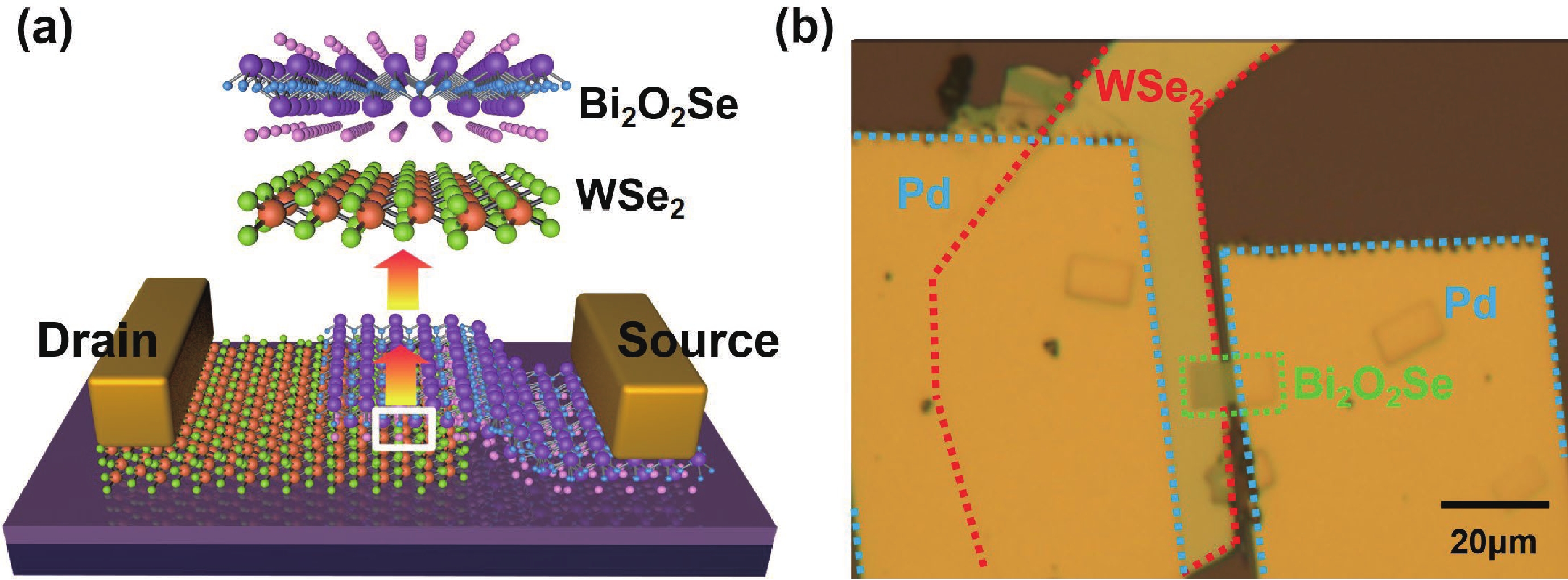
Fig. 1.
(Color online) (a) Schematic diagram of WSe2/Bi2O2Se FET. (b) Optical micrograph of the WSe2/Bi2O2Se FET.
ARTICLES
Ruonan Li1, Fangchao Lu1, Jiajun Deng1, Xingqiu Fu1, Wenjie Wang1, and He Tian2,
Corresponding author: Wenjie Wang, wwj2008@ncepu.edu.cn; He Tian, tianhe88@tsinghua.edu.cn
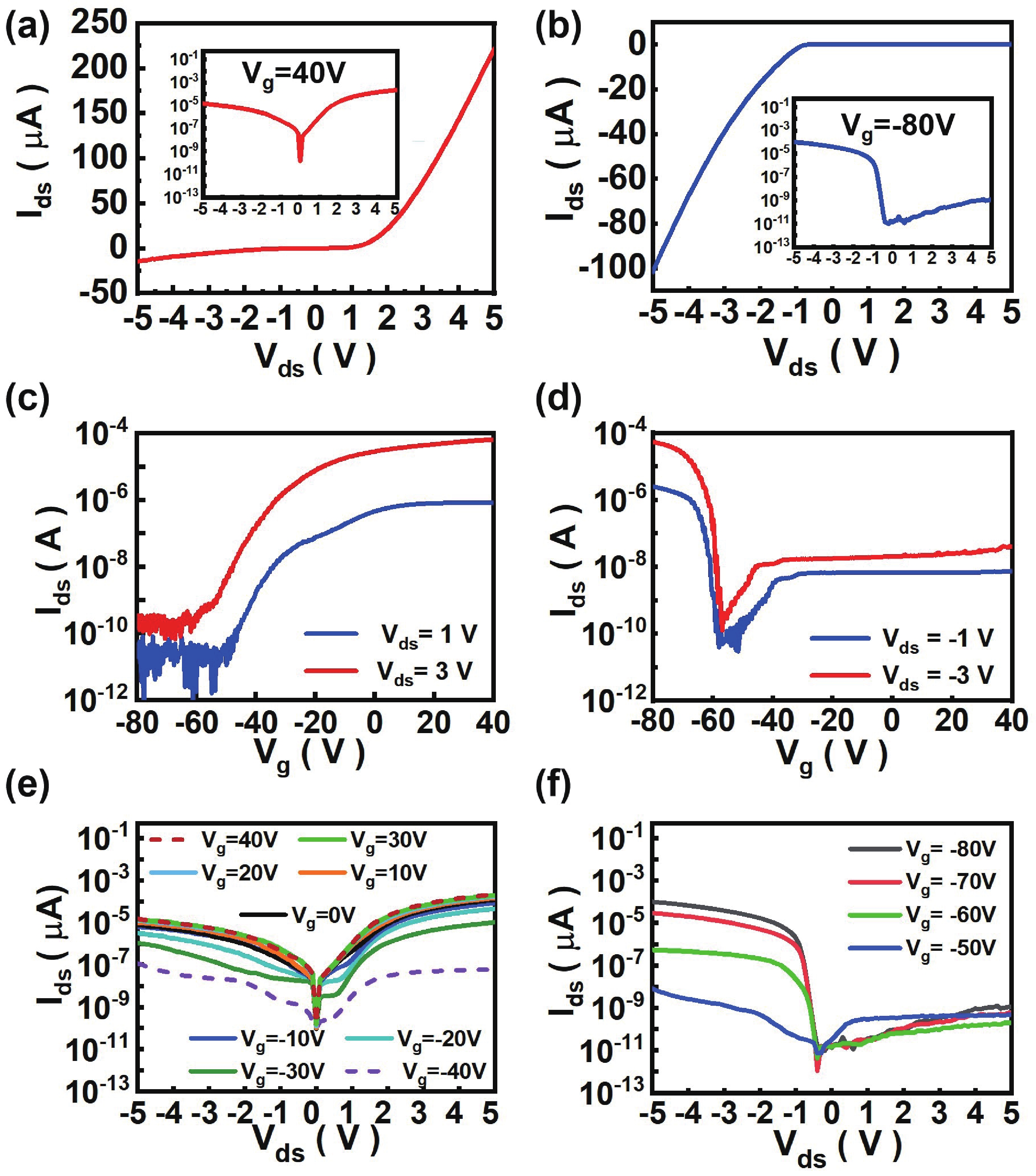
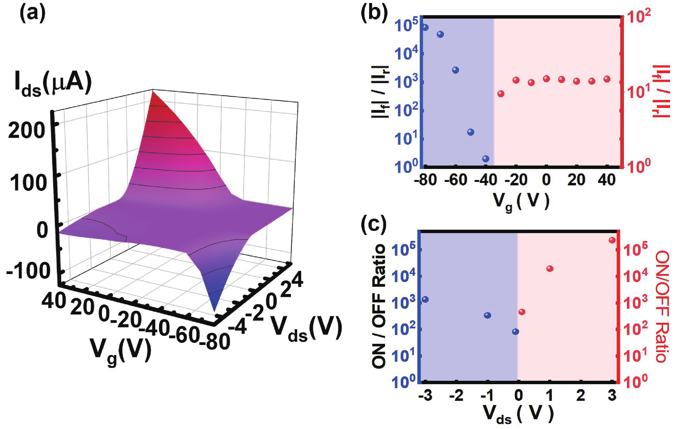
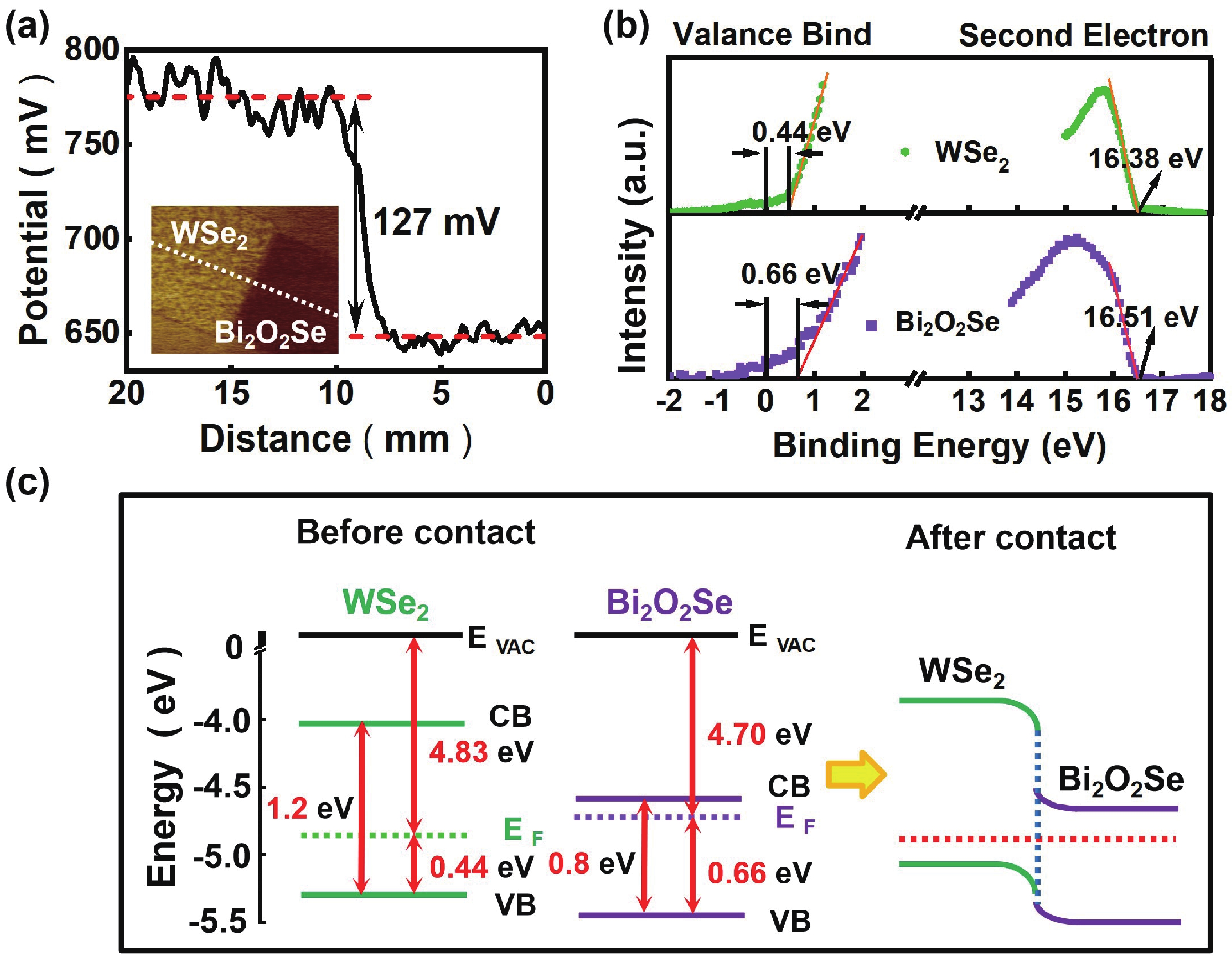
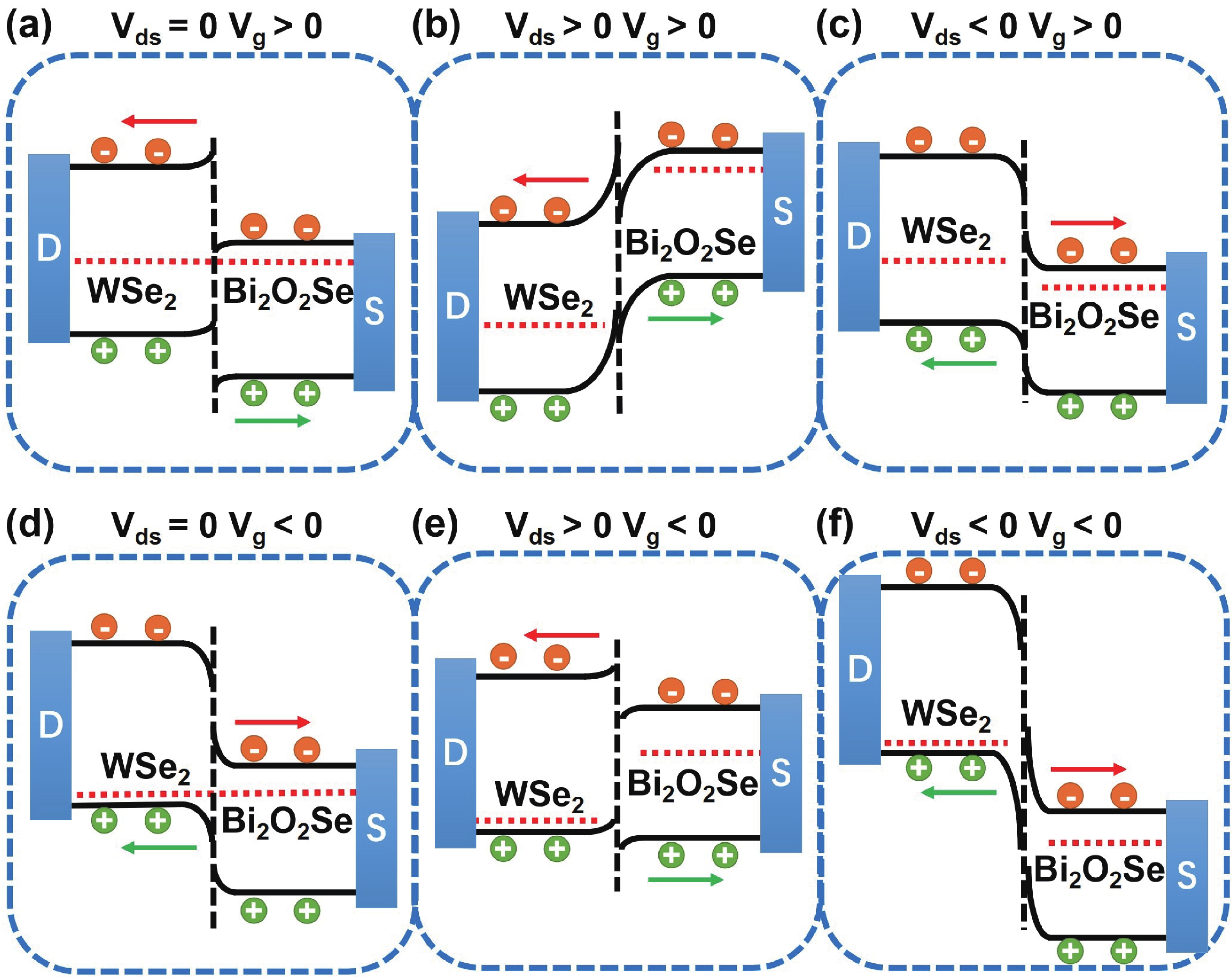
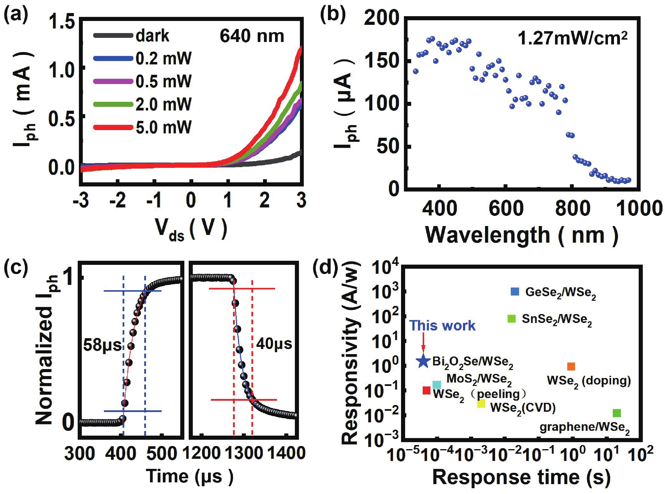
Abstract: Two-dimensional (2D) WSe2 has received increasing attention due to its unique optical properties and bipolar behavior. Several WSe2-based heterojunctions exhibit bidirectional rectification characteristics, but most devices have a lower rectification ratio. In this work, the Bi2O2Se/WSe2 heterojunction prepared by us has a type Ⅱ band alignment, which can vastly suppress the channel current through the interface barrier so that the Bi2O2Se/WSe2 heterojunction device has a large rectification ratio of about 105. Meanwhile, under different gate voltage modulation, the current on/off ratio of the device changes by nearly five orders of magnitude, and the maximum current on/off ratio is expected to be achieved 106. The photocurrent measurement reveals the behavior of recombination and space charge confinement, further verifying the bidirectional rectification behavior of heterojunctions, and it also exhibits excellent performance in light response. In the future, Bi2O2Se/WSe2 heterojunction field-effect transistors have great potential to reduce the volume of integrated circuits as a bidirectional controlled switching device.
Keywords: Bi2O2Se, WSe2, heterojunction, bidirectional rectification, optoelectronic devices
| [1] |
Cheng R, Li D H, Zhou H L, et al. Electroluminescence and photocurrent generation from atomically sharp WSe2/MoS2 heterojunction p–n diodes. Nano Letters, 2014, 14(10), 5590 doi: 10.1021/nl502075n
|
| [2] |
Xiao J W, Zhang Y, Chen H J, et al. Enhanced performance of a monolayer MoS2/WSe2 heterojunction as a photoelectrochemical cathode. Nano-Micro Letters, 2018, 10(4), 60 doi: 10.1007/s40820-018-0212-6
|
| [3] |
Deng Y X, Luo Z, Conrad N J, et al. Black phosphorus–monolayer MoS2 van der waals heterojunction p–n diode. ACS Nano, 2014, 8(8), 8292 doi: 10.1021/nn5027388
|
| [4] |
Deng J Q, Cheng H, Wang C, et al. Evaluation and comprehensive comparison of H-bridge-based bidirectional rectifier and unidirectional rectifiers. Electronics, 2020, 9, 309 doi: 10.3390/electronics9020309
|
| [5] |
Wang Z G, Li Q, Chen Y F, et al. The ambipolar transport behavior of WSe2 transistors and its analogue circuits. NPG Asia Mater, 2018, 10(8), 703 doi: 10.1038/s41427-018-0062-1
|
| [6] |
Wu F, Li Q, Wang P, et al. High efficiency and fast van der Waals hetero-photodiodes with a unilateral depletion region. Nat Commun, 2019, 10(1), 4663 doi: 10.1038/s41467-019-12707-3
|
| [7] |
Pudasaini P R, Stanford M G, Oyedele A, et al. High performance top-gated multilayer WSe2 field effect transistors. Nanotechnology, 2017, 28(47), 475202 doi: 10.1088/1361-6528/aa8081
|
| [8] |
Xiao S D, Li M D, Seabaugh A, et al. Vertical heterojunction of MoS2 and WSe2. 72nd Device Research Conference, Santa Barbara, CA, USA, 2014 doi: 10.1109/DRC.2014.6872351
|
| [9] |
Patel A B, Chauhan P, Patel K, et al. Solution-processed uniform MoSe2–WSe2 heterojunction thin film on silicon substrate for superior and tunable photodetection. ACS Sustainable Chem Eng, 2020, 8(12), 4809 doi: 10.1021/acssuschemeng.9b07449
|
| [10] |
Abderrahmane A, Woo C, Jung P G, et al. Multifunctional WSe2/MoSe2/WSe2/MoSe2 heterostructures. Mater Sci Semicond Process, 2024, 169, 107864 doi: 10.1016/j.mssp.2023.107864
|
| [11] |
Yang Z Y, Liao L, Gong F, et al. WSe2/GeSe heterojunction photodiode with giant gate tunability. Nano Energy, 2018, 49, 103 doi: 10.1016/j.nanoen.2018.04.034
|
| [12] |
Aftab S, Samiya, Ul Haq H M, et al. Van der waals multi-heterostructures (PN, PIN, and NPN) for dynamic rectification in 2D materials. Adv Materials Inter, 2020, 7(24), 2001479 doi: 10.1002/admi.202001479
|
| [13] |
Zhou X, Hu X, Yu J, et al. 2D layered material‐based van der Waals heterostructures for optoelectronics. Advanced Functional Materials, 2018, 28(14), 1706587 doi: 10.1002/adfm.201706587
|
| [14] |
Tong T, Chen Y F, Qin S C, et al. Sensitive and ultrabroadband phototransistor based on two-dimensional Bi2O2Se nanosheets. Adv Funct Materials, 2019, 29, 1905806 doi: 10.1002/adfm.201905806
|
| [15] |
Hong C Y, Huang G F, Yao W W, et al. Thickness-modulated in-plane Bi2O2Se homojunctions for ultrafast high-performance photodetectors. Chin Phys B, 2019, 28, 128502 doi: 10.1088/1674-1056/ab4e87
|
| [16] |
Wang Q S, Wen Y, Cai K M, et al. Nonvolatile infrared memory in MoS2/PbS van der Waals heterostructures. Sci Adv, 2018, 4, eaap7916 doi: 10.1126/sciadv.aap7916
|
| [17] |
Zhou X, Hu X Z, Zhou S S, et al. Tunneling diode based on WSe2/SnS2 heterostructure incorporating high detectivity and responsivity. Adv Mater, 2018, 30, 1703286 doi: 10.1002/adma.201703286
|
| [18] |
Luo P, Zhuge F W, Wang F K, et al. PbSe quantum dots sensitized high-mobility Bi2O2Se nanosheets for high-performance and broadband photodetection beyond 2 μm. ACS Nano, 2019, 13, 9028 doi: 10.1021/acsnano.9b03124
|
| [19] |
Wu J X, Yuan H T, Meng M M, et al. High electron mobility and quantum oscillations in non-encapsulated ultrathin semiconducting Bi2O2Se. Nat Nanotechnol, 2017, 12, 530 doi: 10.1038/nnano.2017.43
|
| [20] |
Doan M H, Jin Y, Adhikari S, et al. Charge transport in MoS2/WSe2 van der waals heterostructure with tunable inversion layer. ACS Nano, 2017, 11, 3832 doi: 10.1021/acsnano.7b00021
|
| [21] |
Kang W M, Cho I T, Roh J, et al. High-gain complementary metal-oxide-semiconductor inverter based on multi-layer WSe2 field effect transistors without doping. Semicond Sci Technol, 2016, 31(10), 105001 doi: 10.1088/0268-1242/31/10/105001
|
| [22] |
Fan S D, Yun S J, Yu W J, et al. Tailoring quantum tunneling in a vanadium-doped WSe2/SnSe2 heterostructure. Adv Sci, 2020, 7(3), 1902751 doi: 10.1002/advs.201902751
|
| [23] |
Luo M, Wu F, Long M S, et al. WSe2/Au vertical Schottky junction photodetector with low dark current and fast photoresponse. Nanotechnology, 2018, 29, 444001 doi: 10.1088/1361-6528/aada68
|
| [24] |
Zheng Z Q, Zhang T M, Yao J, et al. Flexible, transparent and ultra-broadband photodetector based on large-area WSe2 film for wearable devices. Nanotechnology, 2016, 27, 225501 doi: 10.1088/0957-4484/27/22/225501
|
| [25] |
Sun M X, Xie D, Sun Y L, et al. Locally hydrazine doped WSe2 p-n junction toward high-performance photodetectors. Nanotechnology, 2018, 29, 015203 doi: 10.1088/1361-6528/aa96e9
|
| [26] |
Xue H, Dai Y Y, Kim W, et al. High photoresponsivity and broadband photodetection with a band-engineered WSe2/SnSe2 heterostructure. Nanoscale, 2019, 11, 3240 doi: 10.1039/C8NR09248F
|
| [27] |
Xu H, Han X Y, Dai X A, et al. High detectivity and transparent few-layer MoS2/glassy-graphene heterostructure photodetectors. Adv Mater, 2018, 30, 1706561 doi: 10.1002/adma.201706561
|
| [28] |
Lee H S, Ahn J, Shim W, et al. 2D WSe2/MoS2 van der Waals heterojunction photodiode for visible-near infrared broadband detection. Appl Phys Lett, 2018, 113, 163102 doi: 10.1063/1.5042440
|


Article views: 1682 Times PDF downloads: 126 Times Cited by: 0 Times
Received: 14 November 2023 Revised: 29 November 2023 Online: Accepted Manuscript: 15 December 2023Uncorrected proof: 18 December 2023Published: 10 January 2024
| Citation: |
Ruonan Li, Fangchao Lu, Jiajun Deng, Xingqiu Fu, Wenjie Wang, He Tian. Bidirectional rectifier with gate voltage control based on Bi2O2Se/WSe2 heterojunction[J]. Journal of Semiconductors, 2024, 45(1): 012701. doi: 10.1088/1674-4926/45/1/012701
****
R N Li, F C Lu, J J Deng, X Q Fu, W J Wang, H Tian. Bidirectional rectifier with gate voltage control based on Bi2O2Se/WSe2 heterojunction[J]. J. Semicond, 2024, 45(1): 012701. doi: 10.1088/1674-4926/45/1/012701

|
 Ruonan Li got her bachelor’s degree in 2020 from BeiHua University and her master’s degree in 2023 from North China Electric Power University. Her research focuses on the growth of 2D transition metal chalcogenides and device preparation
 Wenjie Wang now works at North China Electric Power University and received his Ph.D. in condensed matter physics from the Superlattice Laboratory of the Institute of Semiconductors, Chinese Academy of Sciences in 2007. His current research interests include growth of two-dimensional materials, photoelectric properties and first-principles computation
 He Tian received the Ph.D. degree from the Institute of Microelectronics, Tsinghua University, Beijing, China, in 2015. He is currently an Associate Professor with Tsinghua University. He has co-authored over 200 papers and more than 8000 citations. His current research interests include various 2-D material-based novel nanodevices
| [1] |
Cheng R, Li D H, Zhou H L, et al. Electroluminescence and photocurrent generation from atomically sharp WSe2/MoS2 heterojunction p–n diodes. Nano Letters, 2014, 14(10), 5590 doi: 10.1021/nl502075n
|
| [2] |
Xiao J W, Zhang Y, Chen H J, et al. Enhanced performance of a monolayer MoS2/WSe2 heterojunction as a photoelectrochemical cathode. Nano-Micro Letters, 2018, 10(4), 60 doi: 10.1007/s40820-018-0212-6
|
| [3] |
Deng Y X, Luo Z, Conrad N J, et al. Black phosphorus–monolayer MoS2 van der waals heterojunction p–n diode. ACS Nano, 2014, 8(8), 8292 doi: 10.1021/nn5027388
|
| [4] |
Deng J Q, Cheng H, Wang C, et al. Evaluation and comprehensive comparison of H-bridge-based bidirectional rectifier and unidirectional rectifiers. Electronics, 2020, 9, 309 doi: 10.3390/electronics9020309
|
| [5] |
Wang Z G, Li Q, Chen Y F, et al. The ambipolar transport behavior of WSe2 transistors and its analogue circuits. NPG Asia Mater, 2018, 10(8), 703 doi: 10.1038/s41427-018-0062-1
|
| [6] |
Wu F, Li Q, Wang P, et al. High efficiency and fast van der Waals hetero-photodiodes with a unilateral depletion region. Nat Commun, 2019, 10(1), 4663 doi: 10.1038/s41467-019-12707-3
|
| [7] |
Pudasaini P R, Stanford M G, Oyedele A, et al. High performance top-gated multilayer WSe2 field effect transistors. Nanotechnology, 2017, 28(47), 475202 doi: 10.1088/1361-6528/aa8081
|
| [8] |
Xiao S D, Li M D, Seabaugh A, et al. Vertical heterojunction of MoS2 and WSe2. 72nd Device Research Conference, Santa Barbara, CA, USA, 2014 doi: 10.1109/DRC.2014.6872351
|
| [9] |
Patel A B, Chauhan P, Patel K, et al. Solution-processed uniform MoSe2–WSe2 heterojunction thin film on silicon substrate for superior and tunable photodetection. ACS Sustainable Chem Eng, 2020, 8(12), 4809 doi: 10.1021/acssuschemeng.9b07449
|
| [10] |
Abderrahmane A, Woo C, Jung P G, et al. Multifunctional WSe2/MoSe2/WSe2/MoSe2 heterostructures. Mater Sci Semicond Process, 2024, 169, 107864 doi: 10.1016/j.mssp.2023.107864
|
| [11] |
Yang Z Y, Liao L, Gong F, et al. WSe2/GeSe heterojunction photodiode with giant gate tunability. Nano Energy, 2018, 49, 103 doi: 10.1016/j.nanoen.2018.04.034
|
| [12] |
Aftab S, Samiya, Ul Haq H M, et al. Van der waals multi-heterostructures (PN, PIN, and NPN) for dynamic rectification in 2D materials. Adv Materials Inter, 2020, 7(24), 2001479 doi: 10.1002/admi.202001479
|
| [13] |
Zhou X, Hu X, Yu J, et al. 2D layered material‐based van der Waals heterostructures for optoelectronics. Advanced Functional Materials, 2018, 28(14), 1706587 doi: 10.1002/adfm.201706587
|
| [14] |
Tong T, Chen Y F, Qin S C, et al. Sensitive and ultrabroadband phototransistor based on two-dimensional Bi2O2Se nanosheets. Adv Funct Materials, 2019, 29, 1905806 doi: 10.1002/adfm.201905806
|
| [15] |
Hong C Y, Huang G F, Yao W W, et al. Thickness-modulated in-plane Bi2O2Se homojunctions for ultrafast high-performance photodetectors. Chin Phys B, 2019, 28, 128502 doi: 10.1088/1674-1056/ab4e87
|
| [16] |
Wang Q S, Wen Y, Cai K M, et al. Nonvolatile infrared memory in MoS2/PbS van der Waals heterostructures. Sci Adv, 2018, 4, eaap7916 doi: 10.1126/sciadv.aap7916
|
| [17] |
Zhou X, Hu X Z, Zhou S S, et al. Tunneling diode based on WSe2/SnS2 heterostructure incorporating high detectivity and responsivity. Adv Mater, 2018, 30, 1703286 doi: 10.1002/adma.201703286
|
| [18] |
Luo P, Zhuge F W, Wang F K, et al. PbSe quantum dots sensitized high-mobility Bi2O2Se nanosheets for high-performance and broadband photodetection beyond 2 μm. ACS Nano, 2019, 13, 9028 doi: 10.1021/acsnano.9b03124
|
| [19] |
Wu J X, Yuan H T, Meng M M, et al. High electron mobility and quantum oscillations in non-encapsulated ultrathin semiconducting Bi2O2Se. Nat Nanotechnol, 2017, 12, 530 doi: 10.1038/nnano.2017.43
|
| [20] |
Doan M H, Jin Y, Adhikari S, et al. Charge transport in MoS2/WSe2 van der waals heterostructure with tunable inversion layer. ACS Nano, 2017, 11, 3832 doi: 10.1021/acsnano.7b00021
|
| [21] |
Kang W M, Cho I T, Roh J, et al. High-gain complementary metal-oxide-semiconductor inverter based on multi-layer WSe2 field effect transistors without doping. Semicond Sci Technol, 2016, 31(10), 105001 doi: 10.1088/0268-1242/31/10/105001
|
| [22] |
Fan S D, Yun S J, Yu W J, et al. Tailoring quantum tunneling in a vanadium-doped WSe2/SnSe2 heterostructure. Adv Sci, 2020, 7(3), 1902751 doi: 10.1002/advs.201902751
|
| [23] |
Luo M, Wu F, Long M S, et al. WSe2/Au vertical Schottky junction photodetector with low dark current and fast photoresponse. Nanotechnology, 2018, 29, 444001 doi: 10.1088/1361-6528/aada68
|
| [24] |
Zheng Z Q, Zhang T M, Yao J, et al. Flexible, transparent and ultra-broadband photodetector based on large-area WSe2 film for wearable devices. Nanotechnology, 2016, 27, 225501 doi: 10.1088/0957-4484/27/22/225501
|
| [25] |
Sun M X, Xie D, Sun Y L, et al. Locally hydrazine doped WSe2 p-n junction toward high-performance photodetectors. Nanotechnology, 2018, 29, 015203 doi: 10.1088/1361-6528/aa96e9
|
| [26] |
Xue H, Dai Y Y, Kim W, et al. High photoresponsivity and broadband photodetection with a band-engineered WSe2/SnSe2 heterostructure. Nanoscale, 2019, 11, 3240 doi: 10.1039/C8NR09248F
|
| [27] |
Xu H, Han X Y, Dai X A, et al. High detectivity and transparent few-layer MoS2/glassy-graphene heterostructure photodetectors. Adv Mater, 2018, 30, 1706561 doi: 10.1002/adma.201706561
|
| [28] |
Lee H S, Ahn J, Shim W, et al. 2D WSe2/MoS2 van der Waals heterojunction photodiode for visible-near infrared broadband detection. Appl Phys Lett, 2018, 113, 163102 doi: 10.1063/1.5042440
|
 appendix 23110014.pdf
|

|

 WeChat ID
Journal of Semiconductors © 2017 All Rights Reserved 京ICP备05085259号-2

 DownLoad:

