J. Semicond. > 2024, Volume 45 > Issue 5 > 052302

ARTICLES

A novel small-signal equivalent circuit model for GaN HEMTs incorporating a dual-field-plate

Jinye Wang, Jun Liu and Zhenxin Zhao

+ Author Affiliations

 Corresponding author: Jun Liu, ljun77@hdu.edu.cn

DOI: 10.1088/1674-4926/45/5/052302

PDF

Turn off MathJax

Abstract: An accurate and novel small-signal equivalent circuit model for GaN high-electron-mobility transistors (HEMTs) is proposed, which considers a dual-field-plate (FP) made up of a gate-FP and a source-FP. The equivalent circuit of the overall model is composed of parasitic elements, intrinsic transistors, gate-FP, and source-FP networks. The equivalent circuit of the gate-FP is identical to that of the intrinsic transistor. In order to simplify the complexity of the model, a series combination of a resistor and a capacitor is employed to represent the source-FP. The analytical extraction procedure of the model parameters is presented based on the proposed equivalent circuit. The verification is carried out on a 4 × 250 μm GaN HEMT device with a gate-FP and a source-FP in a 0.45 μm technology. Compared with the classic model, the proposed novel small-signal model shows closer agreement with measured S-parameters in the range of 1.0 to 18.0 GHz.

Key words: small-signal modeldual field-plate(FP)GaN high-electron-mobility transistors (HEMT)parameter extraction


[1]
He J Q, Cheng W C, Wang Q, et al. Recent advances in GaN-based power HEMT devices. Adv Elect Mater, 2021, 7, 2001045 doi: 10.1002/aelm.202001045
[2]
Bahat-Treidel E, Hilt O, Brunner F, et al. AlGaN/GaN/AlGaN DH-HEMTs breakdown voltage enhancement using multiple grating field plates (MGFPs). IEEE Trans Electron Devices, 2010, 57, 1208 doi: 10.1109/TED.2010.2045705
[3]
Hu Q Y, Zeng F M, Cheng W C, et al. Reducing dynamic on-resistance of p-GaN gate HEMTs using dual field plate configurations. IEEE International Symposium on the Phys and Failure Analysis of Integrated Circuits (IPFA), 2020, 1 doi: 10.1109/IPFA49335.2020.9260581
[4]
Wu Y F, Saxler A, Moore M, et al. 30-W/mm GaN HEMTs by field plate optimization. IEEE Electron Device Lett, 2004, 25, 117 doi: 10.1109/LED.2003.822667
[5]
Xie G, Xu E, Lee J M, et al. Breakdown-voltage-enhancement technique for RF-based AlGaN/GaN HEMTs with a source-connected air-bridge field plate. IEEE Electron Device Lett, 2012, 33, 670 doi: 10.1109/LED.2012.2188492
[6]
Mao W, Fan J S, Du M, et al. Analysis of the modulation mechanisms of the electric field and breakdown performance in AlGaN/GaN HEMT with a T-shaped field-plate. Chinese Phys B, 2016, 25, 127305 doi: 10.1088/1674-1056/25/12/127305
[7]
Boles T, Carlson D, Xia L, et al. Effect of multi-field plates on the reverse breakdown and leakage characteristics of GaN-on-silicon HEMTs. Int Conference on Compound Semicond Manufacturing Technology, Denver, Colorado, 2014, 104
[8]
Amit M, Rawal D S, Sharma S, et al. Design and fabrication of multi-finger field plate for enhancement of AlGaN/GaN HEMT breakdown voltage. Def Sci J, 2018, 68, 290 doi: 10.14429/dsj.68.12134
[9]
Neha, Kumari V, Gupta M, et al. TCAD-based optimization of field plate length & passivation layer of AlGaN/GaN HEMT for higher cut-off frequency & breakdown voltage. IETE Tech Rev, 2022, 39, 63 doi: 10.1080/02564602.2020.1824624
[10]
Liu S J, Duan X L, Wang S L, et al. Optimization of dual field plate AlGaN/GaN HEMTs using artificial neural networks and particle swarm optimization algorithm. IEEE Trans Device Mater Reliab, 2023, 23, 204 doi: 10.1109/TDMR.2023.3246053
[11]
Marinković Z, Crupi G, Caddemi A, et al. A review on the artificial neural network applications for small-signal modeling of microwave FETs. Int J Numerical Modelling, 2020, 33, e2668 doi: 10.1002/jnm.2668
[12]
Khusro A, Husain S, Hashmi M S, et al. A reliable and fast ANN based behavioral modeling approach for GaN HEMT. Int Conference on Synthesis, Modeling, Analysis and Simulation Methods and Appl Circuit Design (SMACD), Lausanne, Switzerland, 2019, 277 doi: 10.1109/SMACD.2019.8795247
[13]
Khusro A, Husain S, Hashmi M S, et al. Small signal behavioral modeling technique of GaN high electron mobility transistor using artificial neural network: An accurate, fast, and reliable approach. Int J RF Microw Comput Aided Eng, 2020, 30, e22112 doi: 10.1002/mmce.22112
[14]
Khusro A, Husain S, Hashmi M S, et al. A generic and efficient globalized kernel mapping-based small-signal behavioral modeling for GaN HEMT. IEEE Access, 2020, 8, 195046 doi: 10.1109/ACCESS.2020.3033788
[15]
Guan R L, Zhu H S, Che W Q, et al. An improved parameter extraction approach for GaN HEMT small-signal modelling. 2020 IEEE MTT-S International Wireless Symposium (IWS), Harbin, China, 2022, 1 doi: 10.1109/IWS55252.2022.9977881
[16]
Fan Q, Leach J H, Morkoc H. Small signal equivalent circuit modeling for AlGaN/GaN HFET: Hybrid extraction method for determining circuit elements of AlGaN/GaN HFET. Proc IEEE, 2010, 98, 1140 doi: 10.1109/JPROC.2010.2044630
[17]
Majumder A, Chatterjee S, Chatterjee S, et al. Optimization of small-signal model of GaN HEMT by using evolutionary algorithms. IEEE Microw Wirel Compon Lett, 2017, 27, 362 doi: 10.1109/LMWC.2017.2678437
[18]
Du J F, Wang K, Yin C G, et al. Small signal modeling of 90 nm gate-length AlGaN/GaN HEMTs considering mesa edge effects. 2014 IEEE International Conference on Electron Devices and Solid-State Circuits, Chengdu, China, 2014, 1 doi: 10.1109/EDSSC.2014.7061240
[19]
Jia Y H, Xu Y H, Wu Y Q, et al. A robust small-signal equivalent circuit model for AlGaN/GaN HEMTs up to 110 GHz. 2016 IEEE MTT-S International Microwave Workshop Series on Advanced Materials and Processes for RF and THz Applications (IMWS-AMP), Chengdu, China, 2016, 1 doi: 10.1109/IMWS-AMP.2016.7588419
[20]
Pei Y, Al-Saman A A, Yin C G, et al. An intrinsic small-signal equivalent circuit model for AlGaN/GaN HEMT considering the momentum balance equation. IEEE J Electron Devices Soc, 2021, 9, 1060 doi: 10.1109/JEDS.2021.3124327
[21]
Karmalkar S, Mishra U K. Enhancement of breakdown voltage in AlGaN/GaN high electron mobility transistors using a field plate. IEEE Trans Electron Devices, 2001, 48, 1515 doi: 10.1109/16.936500
[22]
Wen Z, Xu Y H, Wang C S, et al. An efficient parameter extraction method for GaN HEMT small-signal equivalent circuit model. Int J Numerical Modelling, 2017, 30, e2127 doi: 10.1002/jnm.2127
[23]
White P M, Healy R M. Improved equivalent circuit for determination of MESFET and HEMT parasitic capacitances from "Coldfet" measurements. IEEE Microw Guid Wave Lett, 1993, 3, 453 doi: 10.1109/75.251398
[24]
Jarndal A, Kompa G. A new small-signal modeling approach applied to GaN devices. IEEE Trans Microw Theory Tech, 2005, 53, 3440 doi: 10.1109/TMTT.2005.857332
[25]
Liu J, Ren K, Sun L L, et al. A novel small-signal model for bulk FinFETs accommodating self-heating behaviors. IEEE Electron Device Lett, 2017, 38, 839 doi: 10.1109/LED.2017.2707283
[26]
Wang J Y, Liu J, Chen Z F, et al. An accurate parameter extraction method for small signal model of CNFET. Int J Numerical Modelling, 2021, 34, e2896 doi: 10.1002/jnm.2896
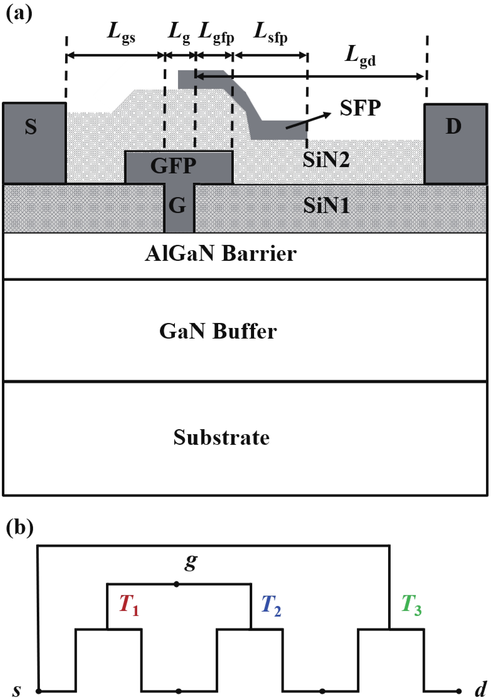
Fig. 1.  (Color online) (a) Cross section of the dual-field-plated GaN HEMT. (b) The equivalent circuit for the model with intrinsic transistor, gate-FP and source-FP.

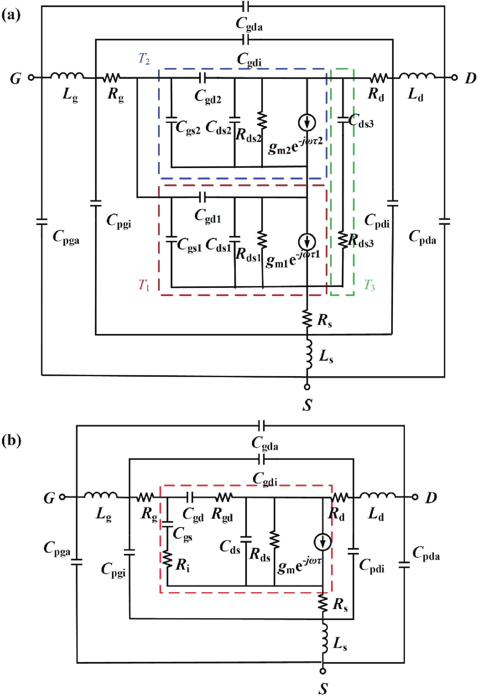
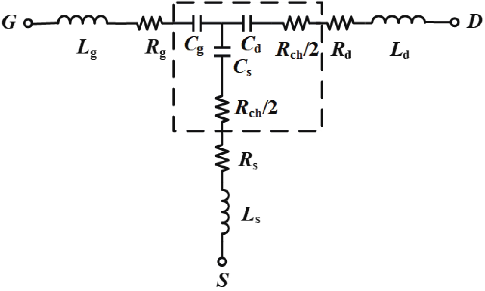
Fig. 2.  (Color online) (a) The novel complete small-signal equivalent circuit of a dual-field-plate GaN HEMT. (b) A classical small signal equivalent circuit model[22].

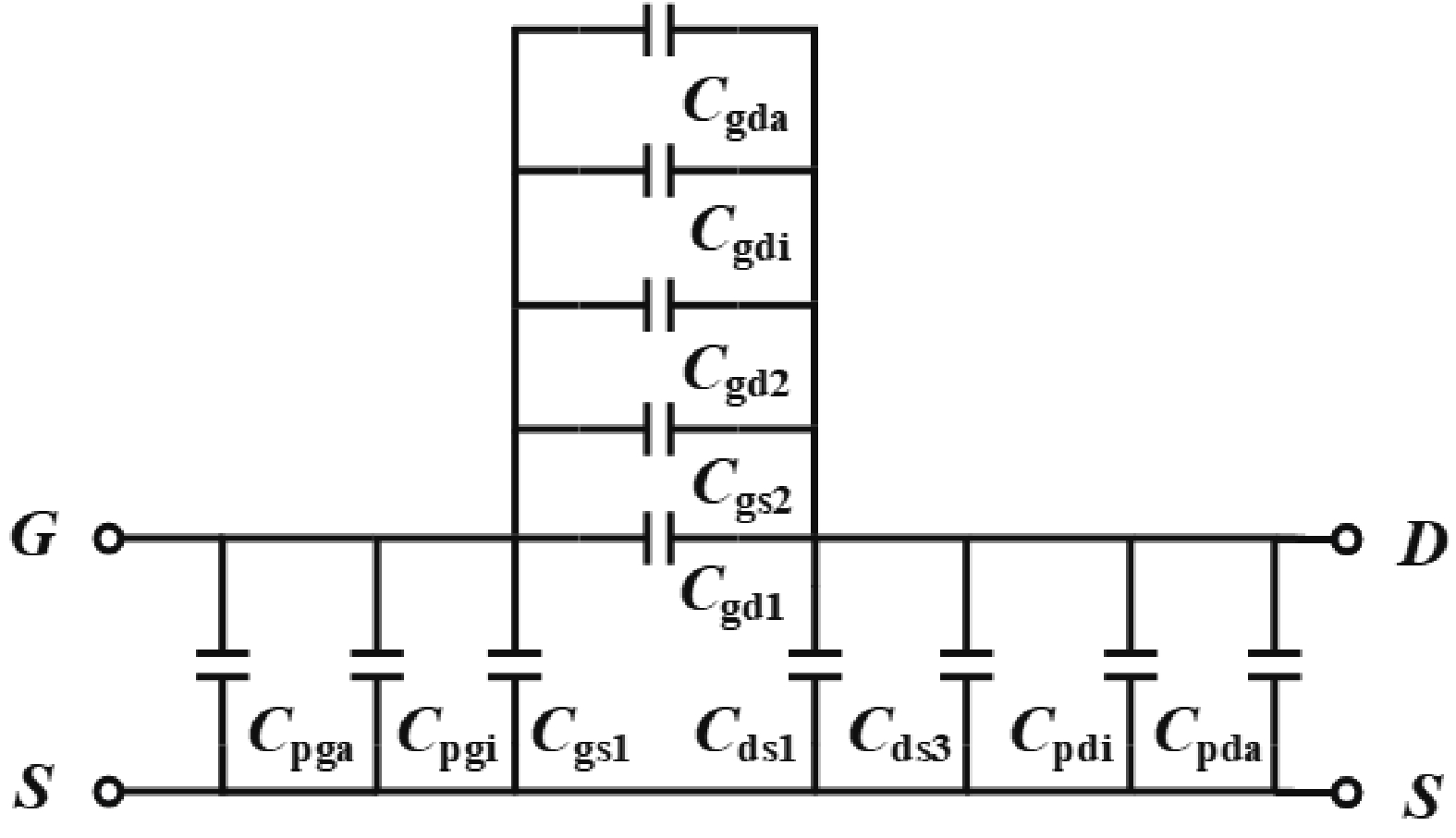
Fig. 3.  Π-network cold pinch-off equivalent circuit for the dual-FP GaN HEMT at low frequency.

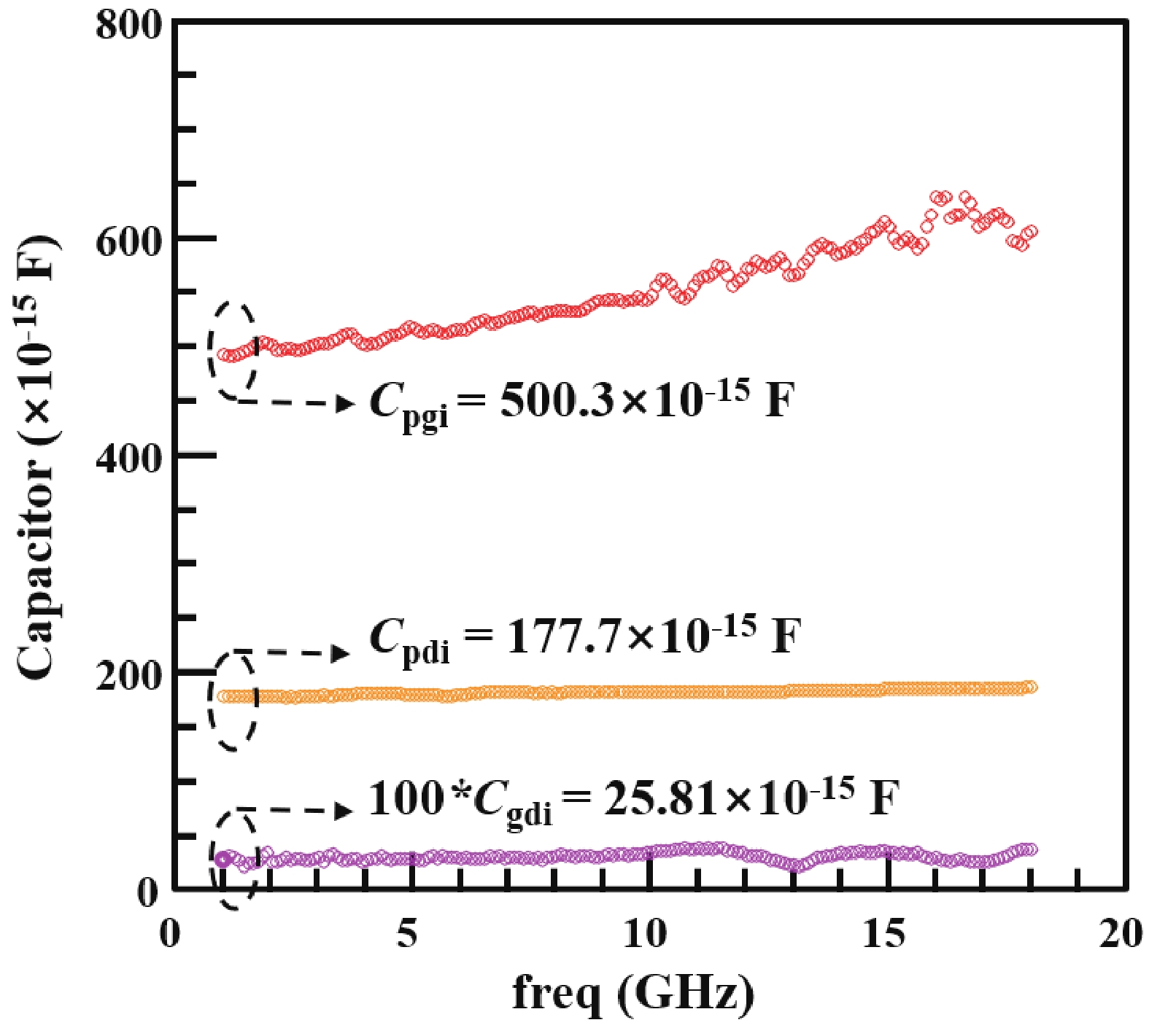
Fig. 4.  (Color online) Capacitance estimation for a 4 × 250 μm dual-field-plate GaN HEMT at Vds = 0 V and Vgs = −5 V.

Fig. 5.  T-network cold pinch-off equivalent circuit for the dual-FP GaN HEMT at high frequency.

Fig. 6.  (Color online) Inductance estimation for a 4 × 250 μm dual-field-plate GaN HEMT at Vds = 0 V and Vgs = 2 V. Symbols: measured data. Lines: model simulation.

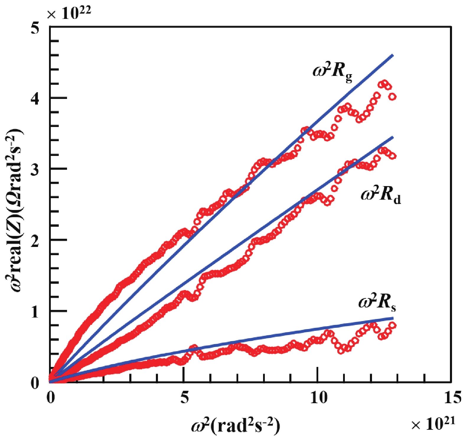
Fig. 7.  (Color online) Resistance estimation for a 4 × 250 μm dual-field-plate GaN HEMT at Vds = 0 V and Vgs = 2 V. Symbols: measured data. Lines: model simulation.

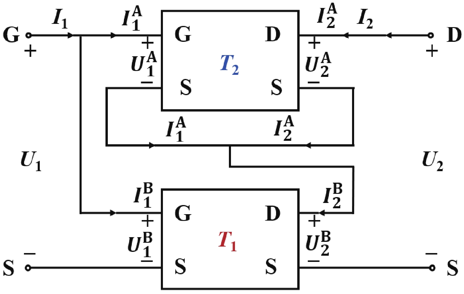
Fig. 8.  (Color online) The equivalent circuit of Tint.

Fig. 9.  (Color online) Measured DC characteristics of the dual-FP GaN HEMT with 800 ns pulse. Vds from 0 to 60 V, step = 2 V; Vgs from −5 to 1 V, step = 0.5 V. (a) Output characteristic; (b) transfer characteristic.

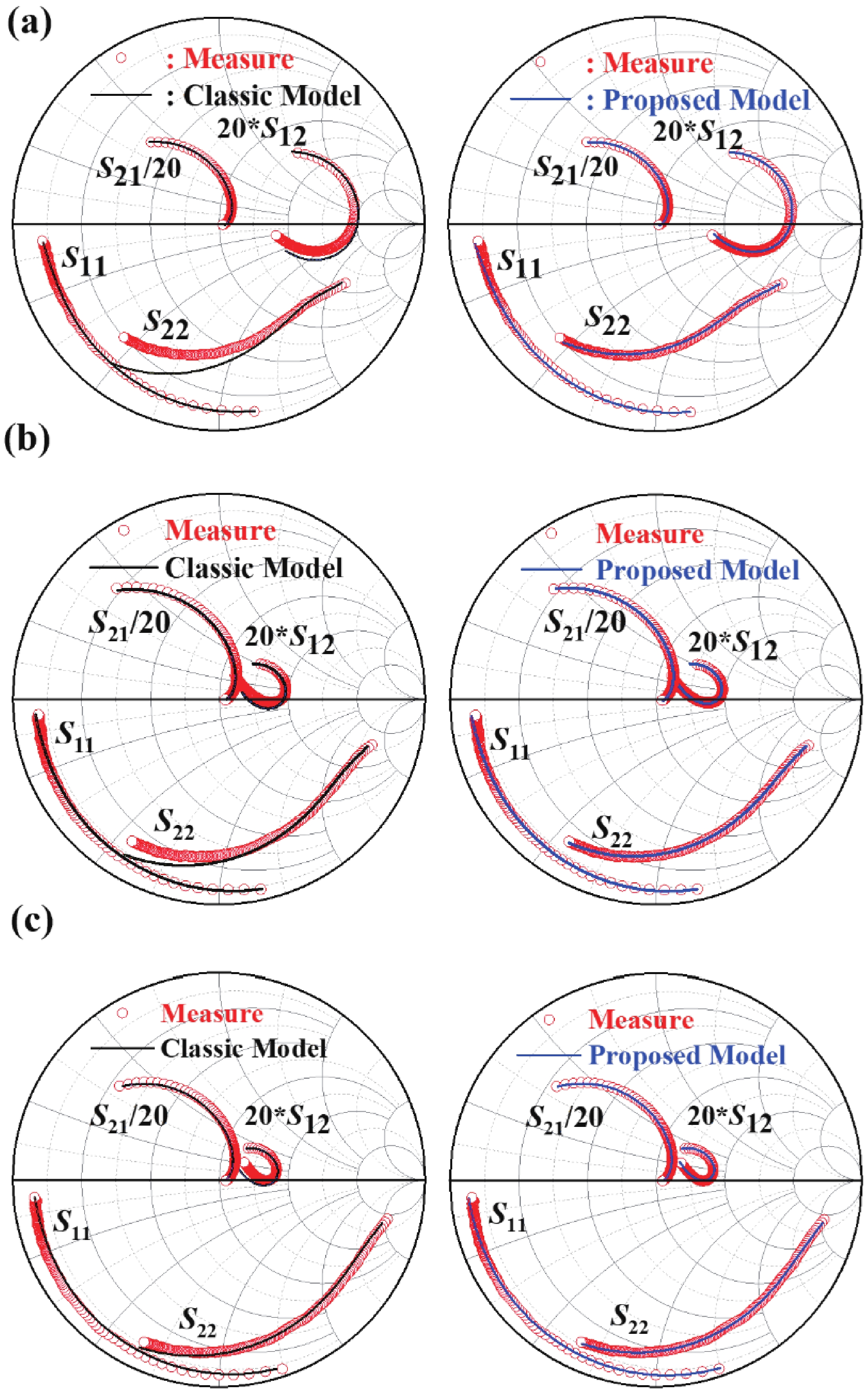
Fig. 10.  (Color online) Measured and modeled S-parameters for a 4 × 250 μm dual-field-plate GaN HEMT under the bias condition of (a) Vds = 28 V, Vgs = 1 V; (b) Vds = 40 V, Vgs = −1 V; (c) Vds = 48 V, Vgs = −3 V. The frequency range is 1−18 GHz.

Table 1.   The proposed and classical small-signal model parameters’ initially extracted and optimized values for a 4 × 250 μm dual-field-plate GaN HEMT.

Parameter Extracted value Optimized parameter
Extrinsic parameters
Cpga, Cgda, Cpda (fF) 50.67, 0.1297, 59.22 50.67, 0.1297, 59.22
Proposed model
(Classic model)
Cpgi, Cgdi, Cpdi (fF) 500.3, 0.2581, 177.7 508.5(375.7), 0.258(0.258), 177.7(158.3)
Lg, Ld, Ls (pH) 15.42, 5.318, 2.660 15.42(15.42), 6.783(6.783), 4.288(2.892)
Rg, Rd, Rs (Ω) 3.254, 2.458, 0.6439 3.382(3.382), 2.628(2.458), 0.546(0.635)
Bias-independent parameters at Vds = 28 V, Vgs = 1 V
Proposed model

Cgs1, Cgd1, Cds1 (fF) 1730, 474.4, 38.87 950.9, 229.0, 46.39
Cgs2, Cgd2, Cds2, Cds3 (fF) 474.4, 63.87, 38.87,77.73 338.7, 35.40, 20.31, 134.5
Rds1, Rds2, Rds3 (Ω) 51.89, 375.0, 51.89 16.01, 133.8, 50.01
gm1, gm2 (mS) 144.3, 144.3 202.2, 110.8
τ1, τ2 (pS) 8.599, 8.599 4.309, 3.677
Classic model Cgs, Cgd, Cds (fF) 1952, 57.76, 130.6 1952, 57.76, 137.5
Ri, Rgd, Rds (Ω) 1.654, 12.4, 319.0 1.654, 12.36, 339.1
gm (mS), τ (pS) 144.9, 6.612 180.4, 8.664
Bias-independent parameters at Vds = 40 V, Vgs = −1 V
Proposed model Cgs1, Cgd1, Cds1 (fF) 1665, 480.3, 28.19 913.1, 244.3, 9.731
Cgs2, Cgd2, Cds2, Cds3 (fF) 480.3, 27.25, 28.19, 56.37 539.1, 13.13, 23.39, 60.77
Rds1, Rds2, Rds3 (Ω) 43.7, 651.3, 325.6 6.449, 351.8, 44.1
gm1, gm2 (mS) 179.3, 179.3 207.6, 179.3
τ1, τ2 (pS) 7.714, 7.714 4.609, 3.881
Classic model Cgs, Cgd, Cds (fF) 2113, 32.98, 85.88 2169, 24.37, 114.4
Ri, Rgd, Rds (Ω) 0.8043, 189.8, 491.4 0.2213, 50.89, 446.1
gm (mS), τ (pS) 208.9, 5.676 243.7, 5.087
Bias-independent parameters at Vds = 48 V, Vgs = −3 V
Proposed model

Cgs1, Cgd1, Cds1 (fF) 1837, 528.5, 16.96 976.7, 294.8, 15.50
Cgs2, Cgd2, Cds2, Cds3 (fF) 528.5, 32.31, 16.96, 33.92 660.2, 10.91, 13.66, 104.7
Rds1, Rds2, Rds3 (Ω) 167.8, 721.5, 360.7 8.317, 208.9, 28.45
gm1, gm2 (mS) 191.3, 191.3 288.0, 167.1
τ1, τ2 (pS) 9.060, 9.060 4.307, 3.624
Classic model Cgs, Cgd, Cds (fF) 1872, 26.95, 75.44 2003, 19.96, 100.9
Ri, Rgd, Rds (Ω) 0.2668, 196.4, 815.3 0.1052, 45.61, 621.7
gm (mS), τ (pS) 186.3, 5.507 202.6, 3.837
DownLoad: CSV

Table 2.   Comparison of error of the proposed and the classical model under three different bias conditions.

Bias condition Model E11 (%) E12 (%) E21 (%) E22 (%)
Vds = 28 V,
Vgs = 1 V
Classic model0.57914.6317.7310.56
Proposed model1.5493.1926.8722.393
Vds = 40 V,
Vgs = −1 V
Classic model1.03630.198.845.511
Proposed model1.1764.7974.0722.173
Vds = 48 V,
Vgs = −3 V
Classic model2.01919.1111.524.269
Proposed model1.3149.2844.5112.576
DownLoad: CSV
[1]
He J Q, Cheng W C, Wang Q, et al. Recent advances in GaN-based power HEMT devices. Adv Elect Mater, 2021, 7, 2001045 doi: 10.1002/aelm.202001045
[2]
Bahat-Treidel E, Hilt O, Brunner F, et al. AlGaN/GaN/AlGaN DH-HEMTs breakdown voltage enhancement using multiple grating field plates (MGFPs). IEEE Trans Electron Devices, 2010, 57, 1208 doi: 10.1109/TED.2010.2045705
[3]
Hu Q Y, Zeng F M, Cheng W C, et al. Reducing dynamic on-resistance of p-GaN gate HEMTs using dual field plate configurations. IEEE International Symposium on the Phys and Failure Analysis of Integrated Circuits (IPFA), 2020, 1 doi: 10.1109/IPFA49335.2020.9260581
[4]
Wu Y F, Saxler A, Moore M, et al. 30-W/mm GaN HEMTs by field plate optimization. IEEE Electron Device Lett, 2004, 25, 117 doi: 10.1109/LED.2003.822667
[5]
Xie G, Xu E, Lee J M, et al. Breakdown-voltage-enhancement technique for RF-based AlGaN/GaN HEMTs with a source-connected air-bridge field plate. IEEE Electron Device Lett, 2012, 33, 670 doi: 10.1109/LED.2012.2188492
[6]
Mao W, Fan J S, Du M, et al. Analysis of the modulation mechanisms of the electric field and breakdown performance in AlGaN/GaN HEMT with a T-shaped field-plate. Chinese Phys B, 2016, 25, 127305 doi: 10.1088/1674-1056/25/12/127305
[7]
Boles T, Carlson D, Xia L, et al. Effect of multi-field plates on the reverse breakdown and leakage characteristics of GaN-on-silicon HEMTs. Int Conference on Compound Semicond Manufacturing Technology, Denver, Colorado, 2014, 104
[8]
Amit M, Rawal D S, Sharma S, et al. Design and fabrication of multi-finger field plate for enhancement of AlGaN/GaN HEMT breakdown voltage. Def Sci J, 2018, 68, 290 doi: 10.14429/dsj.68.12134
[9]
Neha, Kumari V, Gupta M, et al. TCAD-based optimization of field plate length & passivation layer of AlGaN/GaN HEMT for higher cut-off frequency & breakdown voltage. IETE Tech Rev, 2022, 39, 63 doi: 10.1080/02564602.2020.1824624
[10]
Liu S J, Duan X L, Wang S L, et al. Optimization of dual field plate AlGaN/GaN HEMTs using artificial neural networks and particle swarm optimization algorithm. IEEE Trans Device Mater Reliab, 2023, 23, 204 doi: 10.1109/TDMR.2023.3246053
[11]
Marinković Z, Crupi G, Caddemi A, et al. A review on the artificial neural network applications for small-signal modeling of microwave FETs. Int J Numerical Modelling, 2020, 33, e2668 doi: 10.1002/jnm.2668
[12]
Khusro A, Husain S, Hashmi M S, et al. A reliable and fast ANN based behavioral modeling approach for GaN HEMT. Int Conference on Synthesis, Modeling, Analysis and Simulation Methods and Appl Circuit Design (SMACD), Lausanne, Switzerland, 2019, 277 doi: 10.1109/SMACD.2019.8795247
[13]
Khusro A, Husain S, Hashmi M S, et al. Small signal behavioral modeling technique of GaN high electron mobility transistor using artificial neural network: An accurate, fast, and reliable approach. Int J RF Microw Comput Aided Eng, 2020, 30, e22112 doi: 10.1002/mmce.22112
[14]
Khusro A, Husain S, Hashmi M S, et al. A generic and efficient globalized kernel mapping-based small-signal behavioral modeling for GaN HEMT. IEEE Access, 2020, 8, 195046 doi: 10.1109/ACCESS.2020.3033788
[15]
Guan R L, Zhu H S, Che W Q, et al. An improved parameter extraction approach for GaN HEMT small-signal modelling. 2020 IEEE MTT-S International Wireless Symposium (IWS), Harbin, China, 2022, 1 doi: 10.1109/IWS55252.2022.9977881
[16]
Fan Q, Leach J H, Morkoc H. Small signal equivalent circuit modeling for AlGaN/GaN HFET: Hybrid extraction method for determining circuit elements of AlGaN/GaN HFET. Proc IEEE, 2010, 98, 1140 doi: 10.1109/JPROC.2010.2044630
[17]
Majumder A, Chatterjee S, Chatterjee S, et al. Optimization of small-signal model of GaN HEMT by using evolutionary algorithms. IEEE Microw Wirel Compon Lett, 2017, 27, 362 doi: 10.1109/LMWC.2017.2678437
[18]
Du J F, Wang K, Yin C G, et al. Small signal modeling of 90 nm gate-length AlGaN/GaN HEMTs considering mesa edge effects. 2014 IEEE International Conference on Electron Devices and Solid-State Circuits, Chengdu, China, 2014, 1 doi: 10.1109/EDSSC.2014.7061240
[19]
Jia Y H, Xu Y H, Wu Y Q, et al. A robust small-signal equivalent circuit model for AlGaN/GaN HEMTs up to 110 GHz. 2016 IEEE MTT-S International Microwave Workshop Series on Advanced Materials and Processes for RF and THz Applications (IMWS-AMP), Chengdu, China, 2016, 1 doi: 10.1109/IMWS-AMP.2016.7588419
[20]
Pei Y, Al-Saman A A, Yin C G, et al. An intrinsic small-signal equivalent circuit model for AlGaN/GaN HEMT considering the momentum balance equation. IEEE J Electron Devices Soc, 2021, 9, 1060 doi: 10.1109/JEDS.2021.3124327
[21]
Karmalkar S, Mishra U K. Enhancement of breakdown voltage in AlGaN/GaN high electron mobility transistors using a field plate. IEEE Trans Electron Devices, 2001, 48, 1515 doi: 10.1109/16.936500
[22]
Wen Z, Xu Y H, Wang C S, et al. An efficient parameter extraction method for GaN HEMT small-signal equivalent circuit model. Int J Numerical Modelling, 2017, 30, e2127 doi: 10.1002/jnm.2127
[23]
White P M, Healy R M. Improved equivalent circuit for determination of MESFET and HEMT parasitic capacitances from "Coldfet" measurements. IEEE Microw Guid Wave Lett, 1993, 3, 453 doi: 10.1109/75.251398
[24]
Jarndal A, Kompa G. A new small-signal modeling approach applied to GaN devices. IEEE Trans Microw Theory Tech, 2005, 53, 3440 doi: 10.1109/TMTT.2005.857332
[25]
Liu J, Ren K, Sun L L, et al. A novel small-signal model for bulk FinFETs accommodating self-heating behaviors. IEEE Electron Device Lett, 2017, 38, 839 doi: 10.1109/LED.2017.2707283
[26]
Wang J Y, Liu J, Chen Z F, et al. An accurate parameter extraction method for small signal model of CNFET. Int J Numerical Modelling, 2021, 34, e2896 doi: 10.1002/jnm.2896
  • Search

    Advanced Search >>

    GET CITATION

    shu

    Export: BibTex EndNote

    Article Metrics

    Article views: 849 Times PDF downloads: 105 Times Cited by: 0 Times

    History

    Received: 20 December 2023 Revised: 18 January 2024 Online: Accepted Manuscript: 23 February 2024Uncorrected proof: 26 February 2024Published: 10 May 2024

    Catalog

      Email This Article

      User name:
      Email:*请输入正确邮箱
      Code:*验证码错误
      Jinye Wang, Jun Liu, Zhenxin Zhao. A novel small-signal equivalent circuit model for GaN HEMTs incorporating a dual-field-plate[J]. Journal of Semiconductors, 2024, 45(5): 052302. doi: 10.1088/1674-4926/45/5/052302 ****J Y Wang, J Liu, and Z X Zhao, A novel small-signal equivalent circuit model for GaN HEMTs incorporating a dual-field-plate[J]. J. Semicond., 2024, 45(5), 052302 doi: 10.1088/1674-4926/45/5/052302
      Citation:
      Jinye Wang, Jun Liu, Zhenxin Zhao. A novel small-signal equivalent circuit model for GaN HEMTs incorporating a dual-field-plate[J]. Journal of Semiconductors, 2024, 45(5): 052302. doi: 10.1088/1674-4926/45/5/052302 ****
      J Y Wang, J Liu, and Z X Zhao, A novel small-signal equivalent circuit model for GaN HEMTs incorporating a dual-field-plate[J]. J. Semicond., 2024, 45(5), 052302 doi: 10.1088/1674-4926/45/5/052302

      A novel small-signal equivalent circuit model for GaN HEMTs incorporating a dual-field-plate

      DOI: 10.1088/1674-4926/45/5/052302
      More Information
      • Jinye Wang received a bachelor's degree from Tianjin University of technology in 2019. In September of this year, she was studying for a master's and doctorate degree at Hangzhou Dianzi University. She focuses on the modeling semiconductor device
      • Jun Liu received his master's degree from Hangzhou Dianzi University in 2006 and his doctor's degree from Dublin City University in 2011. He is now a professor at the School of Electronic Information, Hangzhou Dianzi University. His main research interest includes device equivalent circuit modeling, RF/MMIC design, CAD/EDA tool development
      • Corresponding author: ljun77@hdu.edu.cn
      • Received Date: 2023-12-20
      • Revised Date: 2024-01-18
      • Available Online: 2024-02-23

      Catalog

        /

        DownLoad:  Full-Size Img  PowerPoint
        Return
        Return