


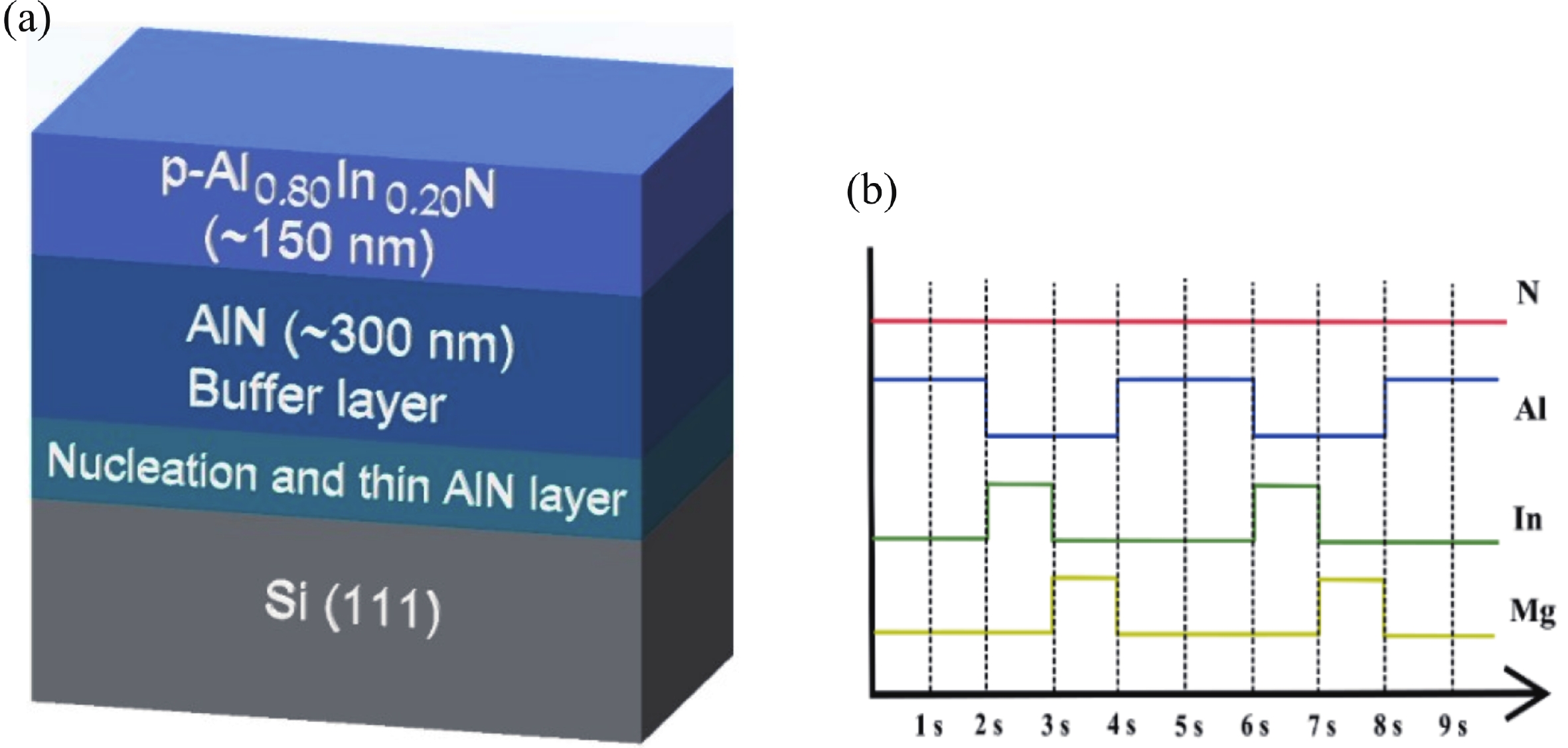
Fig. 1.
(Color online) (a) The proposed structure obtained by MME, and (b) opening−closing shutter sequence used for growing the AlInN layer doped with Mg.
ARTICLES
Horacio Irán Solís-Cisneros1, Carlos Alberto Hernández-Gutiérrez1, , Enrique Campos-González2 and Máximo López-López3
Corresponding author: Carlos Alberto Hernández-Gutiérrez, carlos.hg@tuxtla.tecnm.mx
Abstract: This work reports the growth and characterization of p-AlInN layers doped with Mg by plasma-assisted molecular beam epitaxy (PAMBE). AlInN was grown with an Al molar fraction of 0.80 by metal-modulated epitaxy (MME) with a thickness of 180 nm on Si(111) substrates using AlN as buffer layers. Low substrate temperatures were used to enhance the incorporation of indium atoms into the alloy without clustering, as confirmed by X-ray diffraction (XRD). Cathodoluminescence measurements revealed ultraviolet (UV) range emissions. Meanwhile, Hall effect measurements indicated a maximum hole mobility of 146 cm2/(V∙s), corresponding to a free hole concentration of 1.23 × 1019 cm−3. The samples were analyzed by X-ray photoelectron spectroscopy (XPS) estimating the alloy composition and extracting the Fermi level by valence band analysis. Mg-doped AlInN layers were studied for use as the electron-blocking layer (EBL) in LED structures. We varied the Al composition in the EBL from 0.84 to 0.96 molar fraction to assess its theoretical effects on electroluminescence, carrier concentration, and electric field, using SILVACO Atlas. The results from this study highlight the importance and capability of producing high-quality Mg-doped p-AlInN layers through PAMBE. Our simulations suggest that an Al content of 0.86 is optimal for achieving desired outcomes in electroluminescence, carrier concentration, and electric field.
Keywords: metal-modulated epitaxy, AlInN, DUV-LED, EBL, simulation
| [1] |
Kneissl M, Seong T Y, Han J, et al. The emergence and prospects of deep-ultraviolet light-emitting diode technologies. Nat Photonics, 2019, 13, 233 doi: 10.1038/s41566-019-0359-9
|
| [2] |
Yu H B, Memon M H, Wang D, et al. AlGaN-based deep ultraviolet micro-LED emitting at 275 nm. Opt Lett, 2021, 46, 3271 doi: 10.1364/OL.431933
|
| [3] |
Lowman W, Etheredge H R, Gaylard P, et al. The novel application and effect of an ultraviolet light decontamination strategy on the healthcare acquisition of carbapenem-resistant Enterobacterales in a hospital setting. J Hosp Infect, 2022, 121, 57 doi: 10.1016/j.jhin.2021.12.008
|
| [4] |
Tang L, Tang B, Zhang H, et al. Review—review of research on AlGaN MOCVD growth. ECS J Solid State Sci Technol, 2020, 9, 24009 doi: 10.1149/2162-8777/ab6833
|
| [5] |
Majchrzak D, Gorantla S, Zdanowicz E, et al. Detailed surface studies on the reduction of Al incorporation into AlGaN grown by molecular beam epitaxy in the Ga-droplet regime. Vacuum, 2022, 202, 111168 doi: 10.1016/j.vacuum.2022.111168
|
| [6] |
Zhang Q H, Parimoo H, Martel E, et al. Molecular beam epitaxy of AlGaN epilayers on Si for vertical deep ultraviolet light-emitting diodes. ECS J Solid State Sci Technol. 2022, 11, 1160, 02 doi: 10.1149/2162-8777/aca2d9
|
| [7] |
Adachi M, Fujiwara K, Sekiya R, et al. In situ observations of the dissolution of an AlN film into liquid Al using a high-temperature microscope. Mater Sci Semicond Process, 2022, 142, 106469 doi: 10.1016/j.mssp.2022.106469
|
| [8] |
Kim J G, Cho C, Kim E, et al. High breakdown voltage and low-Current dispersion in AlGaN/GaN HEMTs with high-quality AlN buffer layer. IEEE Trans Electron Devices, 2021, 68, 1513 doi: 10.1109/TED.2021.3057000
|
| [9] |
Klein B A, Baca A G, Lepkowski S M, et al. Saturation velocity measurement of Al0.7Ga0.3N-channel high electron mobility transistors. J Electron Mater, 2019, 48, 5581 doi: 10.1007/s11664-019-07421-1
|
| [10] |
Tsai Y C, Bayram C. Band alignments of ternary wurtzite and zincblende III-nitrides investigated by hybrid density functional theory. ACS Omega, 2020, 5, 3917 doi: 10.1021/acsomega.9b03353
|
| [11] |
Amano H, Collazo R, Santi C, et al. The 2020 UV emitter roadmap. J Phys D Appl Phys, 2020, 53, 503001 doi: 10.1088/1361-6463/aba64c
|
| [12] |
Mohamad R, Ruterana P. 2021 Indium segregation mechanism and V-defect formation at the [0001] InAlN surface: An ab-initio investigation. J Phys D Appl Phys, 2021, 54, 15305 doi: 10.1088/1361-6463/abb621
|
| [13] |
Velpula R T, Jain B, Lenka T R, et al. Polarization-engineered p-type electron-blocking-layer-free III-nitride deep-ultraviolet light-emitting diodes for enhanced carrier transport. J Electron Mate, 2022, 51, 838 doi: 10.1007/s11664-021-09363-z
|
| [14] |
Sharif M N, Niass M I, Liou J J, et al. P-AlInN electron blocking layer for AlGaN-based deep-ultraviolet light-emitting diode. Superlattices Microstruct, 2021, 158, 107022 doi: 10.1016/j.spmi.2021.107022
|
| [15] |
Usman M, Jamil T, Aamir M, et al. Performance enhancement with thin p-AlInN electron-blocking layer in ultraviolet light-emitting diodes. Opt Eng, 2023, 62, 17106 doi: 10.1117/1.OE.62.1.017106
|
| [16] |
Chu C S, Tian K K, Che J M, et al. On the origin of enhanced hole injection for AlGaN-based deep ultraviolet light-emitting diodes with AlN insertion layer in p-electron blocking layer. Opt Express, 2019, 27, A620 doi: 10.1364/OE.27.00A620
|
| [17] |
Jamil T, Usman M. Optimized carrier confinement in deep-ultraviolet light-emitting diodes with AlInGaN/AlInN superlattice electron blocking layer. Mater Sci Eng B, 2022, 278, 115638 doi: 10.1016/j.mseb.2022.115638
|
| [18] |
Yamaguchi Y, Kanitani Y, Kudo Y, et al. Atomic diffusion of indium through threading dislocations in InGaN quantum wells. Nano Lett, 2022, 22, 6930 doi: 10.1021/acs.nanolett.2c01479
|
| [19] |
Camacho-Reynoso M, Hernández-Gutiérrez C A, Yee-Rendón C, et al. Cubic InxGa1−xN/GaN quantum wells grown by migration enhanced epitaxy (MEE) and conventional molecular beam epitaxy (MBE). J Alloys Compd, 2022, 921, 165994 doi: 10.1016/j.jallcom.2022.165994
|
| [20] |
Lu H, Schaff W J, Hwang J, et al. Improvement on epitaxial grown of InN by migration enhanced epitaxy. Appl Phys Lett, 2000, 77, 2548 doi: 10.1063/1.1318235
|
| [21] |
Laleyan D A, Fernández-Delgado N, Reid E T, et al. Strain-free ultrathin AlN epilayers grown directly on sapphire by high-temperature molecular beam epitaxy. Appl Phys Lett, 2020, 116, 152102 doi: 10.1063/1.5144838
|
| [22] |
Ramos L E, Teles L K, Scolfaro L M R, et al. Structural, electronic, and effective-mass properties of silicon and zinc-blende group-III nitride semiconductor compounds. Phys Rev B, 2001, 63, 165210 doi: 10.1103/PhysRevB.63.165210
|
| [23] |
Aleksandrov I A, Malin T V, Zhuravlev K S, et al. Diffusion in GaN/AlN superlattices: DFT and EXAFS study. Appl Surf Sci, 2020, 515, 146001 doi: 10.1016/j.apsusc.2020.146001
|
| [24] |
Jia H, Yang W, Zhang X, Zhou X, et al. Effects and mechanisms of In surfactant on high Al-content AlGaN grown by plasma-assisted molecular beam epitaxy. Opt Express, 2022, 30, 1782 doi: 10.1364/OE.445600
|
| [25] |
Madiomanana K, Bahri M, Rodriguez J B, et al. Silicon surface preparation for III-V molecular beam epitaxy. J Cryst Growth, 2015, 413, 17 doi: 10.1016/j.jcrysgro.2014.12.004
|
| [26] |
Feng Q, Wei W, Zhang B, et al. O-band and C/L-Band III-V Quantum Dot Lasers Monolithically Grown on Ge and Si Substrate. Appl Sci, 2019, 9, 385 doi: 10.3390/app9030385
|
| [27] |
Tournié E, Monge Bartolome L, Rio Calvo M, et al. Mid-infrared III–V semiconductor lasers epitaxially grown on Si substrates Light. Sci Appl, 2022, 11, 165 doi: 10.1038/s41377-022-00850-4
|
| [28] |
Ishizaka A, Shiraki Y. Low temperature surface cleaning of silicon and its application to silicon MBE. J Electrochem Soc, 1986, 133, 666 doi: 10.1149/1.2108651
|
| [29] |
Ahmad H, Motoki K, Clinton E A, et al. Comprehensive analysis of metal modulated epitaxial GaN. ACS Appl Mater Interfaces, 2020, 12, 37693 doi: 10.1021/acsami.0c09114
|
| [30] |
Zambrano-Serrano M A, Hernández C A, de Melo O, et al. Effects of heavy Si doping on the structural and optical properties of n-GaN/AlN/Si(111) heterostructures. Mater Res Express, 2022, 9, 65903 doi: 10.1088/2053-1591/ac7512
|
| [31] |
Ramesh C, Tyagi P, Yadav B S, et al. Effect of nitridation temperature on formation and properties of GaN nanowall networks on sapphire (0 0 0 1) grown by laser MBE. Mater Sci Eng B, 2018, 231, 105 doi: 10.1016/j.mseb.2018.10.009
|
| [32] |
Frei K, Trejo-Hernández R, Schütt S, et al. Investigation of growth parameters for ScAlN-barrier HEMT structures by plasma-assisted MBE. Jpn J Appl Phys, 2019, 58, SC1045 doi: 10.7567/1347-4065/ab124f
|
| [33] |
Hernández-Gutiérrez C A, Casallas-Moreno Y L, Rangel-Kuoppa V T, et al. Study of the heavily p-type doping of cubic GaN with Mg. Sci Rep, 2020, 10, 16858 doi: 10.1038/s41598-020-73872-w
|
| [34] |
Jian Z, Hejing W. The physical meanings of 5 basic parameters for an X-ray diffraction peak and their application. Chinese J Geochemistry, 2003, 22, 38 doi: 10.1007/BF02831544
|
| [35] |
Pandey A, Dalal S, Dutta S, et al. Structural characterization of polycrystalline thin films by X-ray diffraction techniques. J Mater Sci Mater Electron, 2021, 32, 1341 doi: 10.1007/s10854-020-04998-w
|
| [36] |
Alam S N, Zubialevich V Z, Ghafary B, et al. Bandgap and refractive index estimates of InAlN and related nitrides across their full composition ranges. Sci Rep, 2020, 10, 16205 doi: 10.1038/s41598-020-73160-7
|
| [37] |
Terashima W, Che S-B, Ishitani Y, et al. Growth and characterization of AlInN ternary alloys in whole composition range and fabrication of InN/AlInN multiple quantum wells by RF molecular beam epitaxy. Jpn J Appl Phys, 2006, 45, L539 doi: 10.1143/JJAP.45.L539
|
| [38] |
Tsai Y C, Bayram C. Structural and electronic properties of hexagonal and cubic phase AlGaInN alloys investigated using first principles calculations. Sci Rep, 2019, 9, 6593 doi: 10.1038/s41598-019-43048-2
|
| [39] |
Onuma T, Chichibu S F, Uchinuma Y, et al. Recombination dynamics of localized excitons in Al1− xIn xN epitaxial films on GaN templates grown by metalorganic vapor phase epitaxy. J Appl Phys, 2003, 94, 2449 doi: 10.1063/1.1592868
|
| [40] |
Le Roux F, Possémé N, Burtin P, et al. Characterization of AlGaN/GaN degradations during plasma etching for power devices. Microelectron Eng, 2021, 249, 111619 doi: 10.1016/j.mee.2021.111619
|
| [41] |
Tu W, Chen Z, Zhuo Y, et al. Performance optimization of AlGaN-based LEDs by use of ultraviolet-transparent indium tin oxide: Effect of in situ contact treatment. Appl Phys Express, 2018, 11, 52101 doi: 10.7567/APEX.11.052101
|
| [42] |
Hernández-Gutiérrez C A, Kudriavtsev Y, Cardona D, et al. Optical, electrical, and chemical characterization of nanostructured InxGa1-xN formed by high fluence In+ ion implantation into GaN. Opt Mater, 2021, 111, 110541 doi: 10.1016/j.optmat.2020.110541
|
| [43] |
Lü M, Dong C, Wang Y. Proposal and achievement of a relatively Al-rich interlayer for In-rich AlxIn1−xN films deposition. J Wuhan Univ Technol Sci Ed, 2013, 28, 868 doi: 10.1007/s11595-013-0784-4
|
| [44] |
Song W Q, Li T, Zhang L, et al. Influence of growth parameters on microstructures and electrical properties of InxAl1−xN thin films using sputtering. J Alloys Compd, 2021, 885, 160977 doi: 10.1016/j.jallcom.2021.160977
|
| [45] |
Shard A G. Detection limits in XPS for more than 6000 binary systems using Al and Mg Kα X-rays. Sur. Interface Anal, 2014, 46, 175 doi: 10.1002/sia.5406
|
| [46] |
Kraut E A, Grant R W, Waldrop J R, et al. Precise determination of the valence-band edge in X-ray photoemission spectra: Application to measurement of semiconductor interface potentials. Phys Rev Lett, 1980, 44, 1620 doi: 10.1103/PhysRevLett.44.1620
|
| [47] |
Wang W, Chu C, Che J, et al. Is a thin p-GaN layer possible for making high-efficiency AlGaN-based deep-ultraviolet light-emitting diodes? Opt Express, 2021, 29, 29651 doi: 10.1364/OE.434636
|
| [48] |
Solís-Cisneros H I, Hu Y, Camas-Anzueto J L, et al. theoretical and computational analysis of a wurtzite-AlGaN DUV-LED to mitigate quantum-confined Stark effect with a zincblende comparison considering Mg- and Be-doping. Nanomaterials, 2022, 12, 4347 doi: 10.3390/nano12234347
|
| [49] |
Martínez-Revuelta R, Solís-Cisneros H I, Trejo-Hernández R, et al. Numerical study of a solar cell to achieve the highest InGaN power conversion efficiency for the whole In-content range. Micromachines, 2022, 13, 1828 doi: 10.3390/mi13111828
|
| [50] |
Ma N, Wang X Q, Liu S T, et al. Hole mobility in wurtzite InN. Appl Phys Lett, 2011, 98, 18 doi: 10.1063/1.3592257
|
| [51] |
Guo Q, Kirste R, Mita S, et al. The polarization field in Al-rich AlGaN multiple quantum wells. Jpn J Appl Phys, 2019, 58, SCCC10 doi: 10.7567/1347-4065/ab07a9
|
| [52] |
Prodhomme P Y, Beya-Wakata A, Bester G. Nonlinear piezoelectricity in wurtzite semiconductors. Phys Rev B, 2013, 88, 121304 doi: 10.1103/PhysRevB.88.121304
|
| [53] |
Ozgur Ü, Liu H, Li X, et al. GaN-based light-emitting diodes: Efficiency at high injection levels. Proc IEEE, 2010, 98, 1180 doi: 10.1109/JPROC.2010.2043210
|
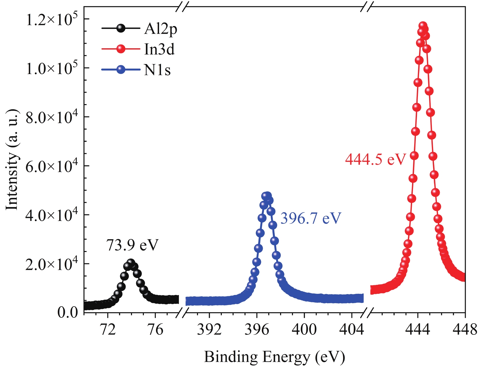
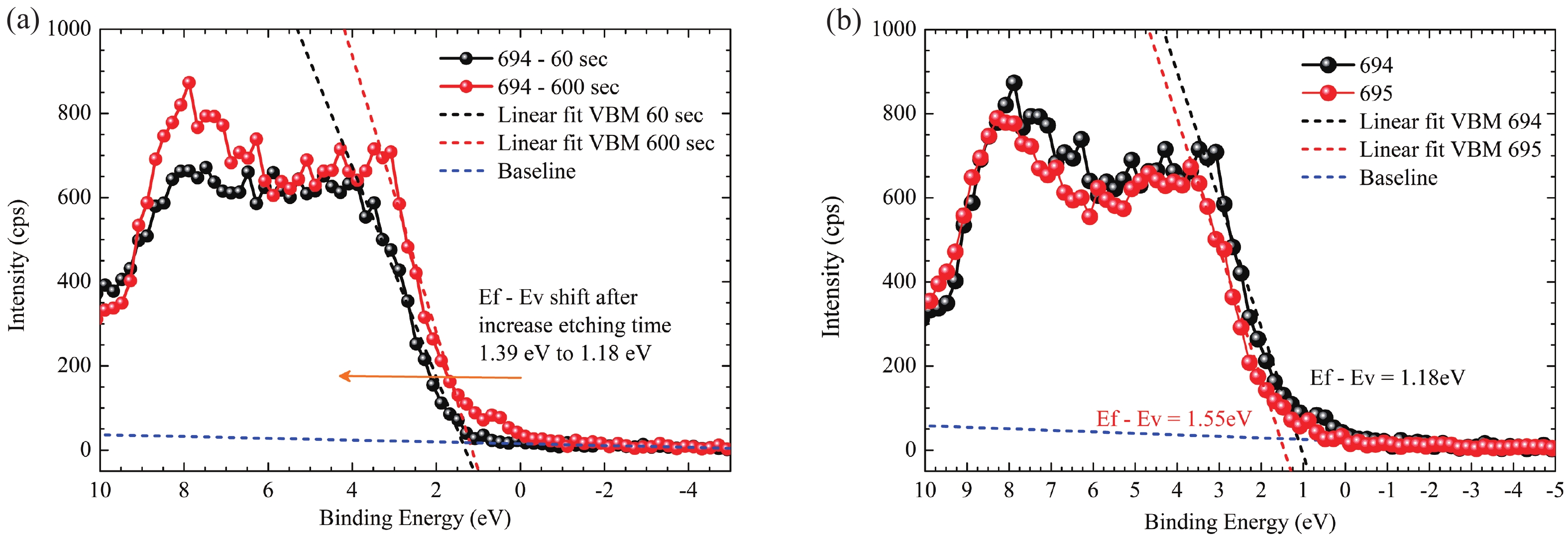
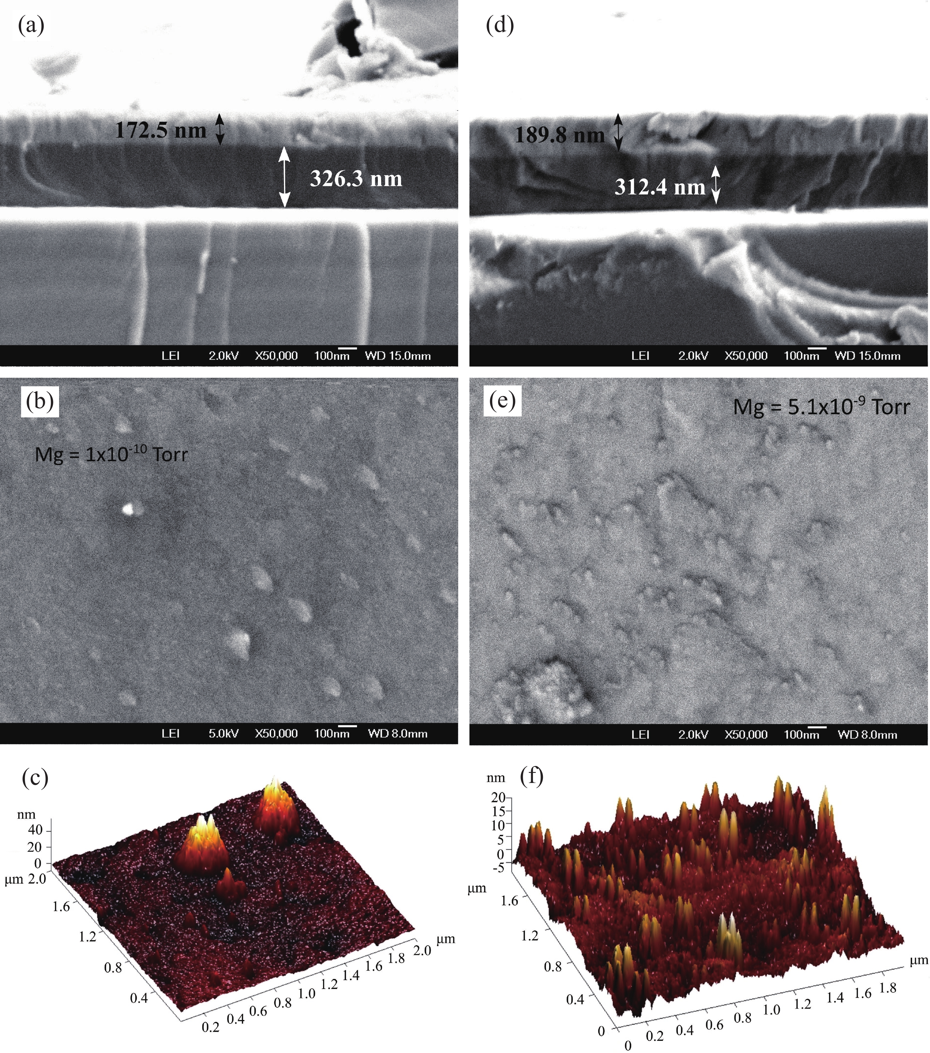
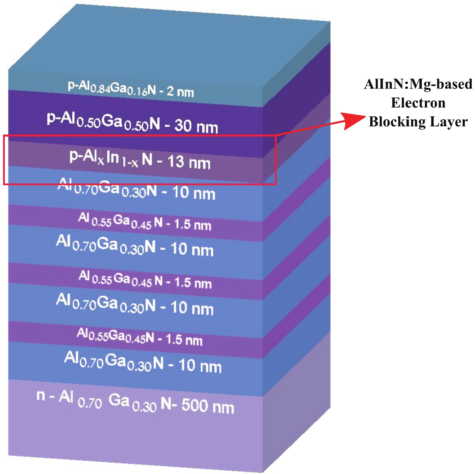
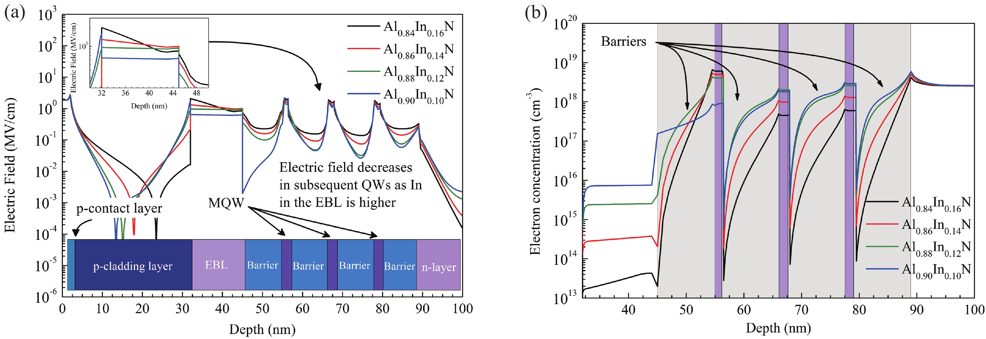
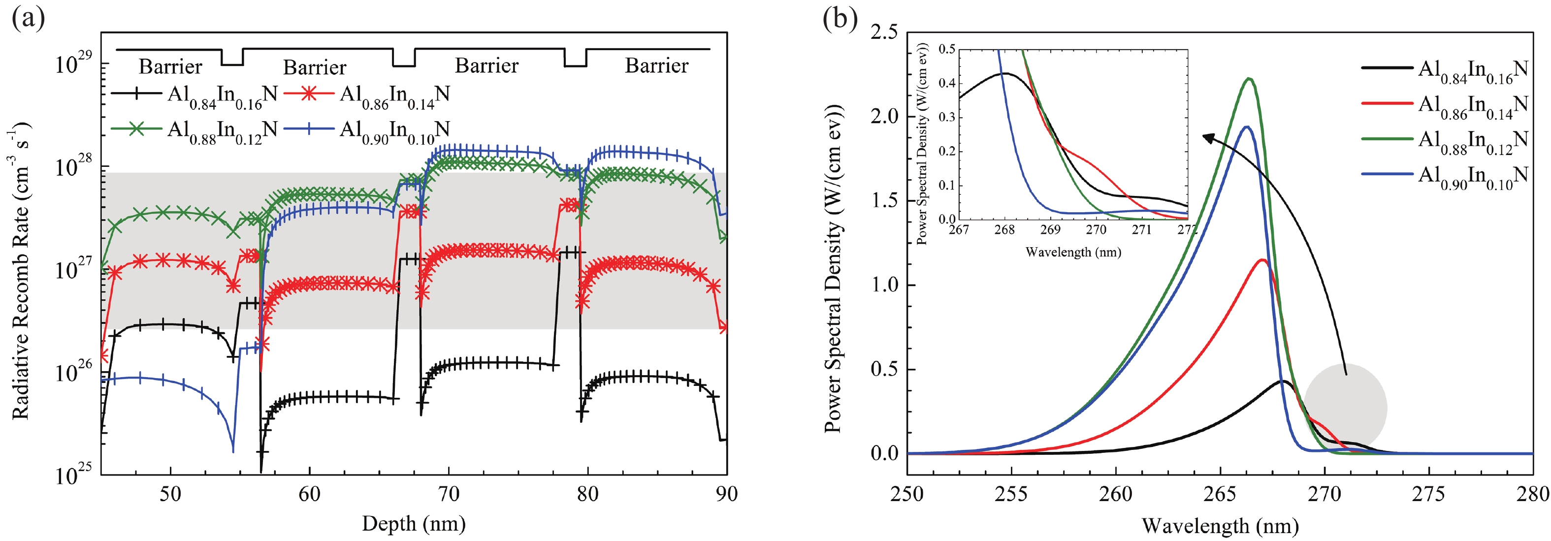
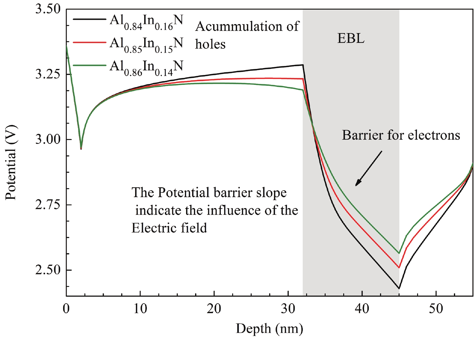
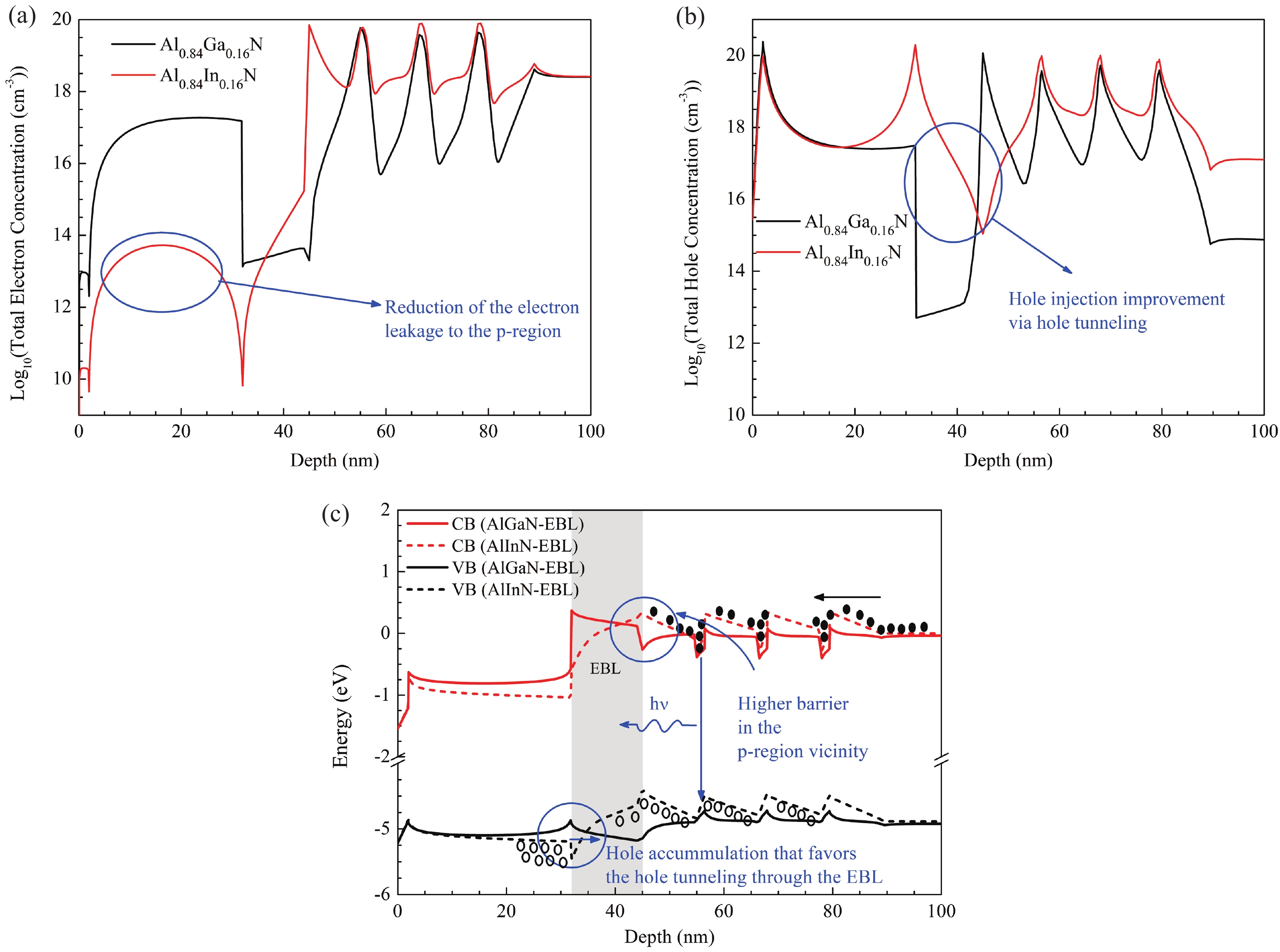
Table 1. Summary of results from XPS analysis of AlInN layers obtained by MME.
| Sample | Element | Atomic (%) | x in ternary alloy AlxIn1−xN | |
| 694 | Al | 45.76 | 0.85 | |
| In | 7.66 | 0.14 | ||
| N | 46.57 | − | ||
| Mg | <0.01 | − | ||
| 695 | Al | 44.74 | 0.83 | |
| In | 9.17 | 0.17 | ||
| N | 46.08 | − | ||
| Mg | <0.01 | − |
 DownLoad: CSV
Table 2. Simulation setup parameters from Refs. [38, 48, 49] (except when it is indicated).
| Parameter | AlN | GaN | InN |
| Eg | 6.2 eV | 3.4 eV | 0.7 eV |
| Affinity | 1.4 eV | 4.0 eV | 5.5 eV |
| Permittivity | 8.5 | 8.9 | 15.3 |
| Electron mobility | 110 cm/(V∙s) | 300 cm/(V∙s) | 2000 cm/(V∙s) |
| Hole mobility | 10 cm/(V∙s) | 14 cm/(V∙s) | 20 cm/(V∙s)[50] |
| Bowing factor | 1.348 eV | 1.775 eV | 3.678 eV |
DownLoad: CSV
| [1] |
Kneissl M, Seong T Y, Han J, et al. The emergence and prospects of deep-ultraviolet light-emitting diode technologies. Nat Photonics, 2019, 13, 233 doi: 10.1038/s41566-019-0359-9
|
| [2] |
Yu H B, Memon M H, Wang D, et al. AlGaN-based deep ultraviolet micro-LED emitting at 275 nm. Opt Lett, 2021, 46, 3271 doi: 10.1364/OL.431933
|
| [3] |
Lowman W, Etheredge H R, Gaylard P, et al. The novel application and effect of an ultraviolet light decontamination strategy on the healthcare acquisition of carbapenem-resistant Enterobacterales in a hospital setting. J Hosp Infect, 2022, 121, 57 doi: 10.1016/j.jhin.2021.12.008
|
| [4] |
Tang L, Tang B, Zhang H, et al. Review—review of research on AlGaN MOCVD growth. ECS J Solid State Sci Technol, 2020, 9, 24009 doi: 10.1149/2162-8777/ab6833
|
| [5] |
Majchrzak D, Gorantla S, Zdanowicz E, et al. Detailed surface studies on the reduction of Al incorporation into AlGaN grown by molecular beam epitaxy in the Ga-droplet regime. Vacuum, 2022, 202, 111168 doi: 10.1016/j.vacuum.2022.111168
|
| [6] |
Zhang Q H, Parimoo H, Martel E, et al. Molecular beam epitaxy of AlGaN epilayers on Si for vertical deep ultraviolet light-emitting diodes. ECS J Solid State Sci Technol. 2022, 11, 1160, 02 doi: 10.1149/2162-8777/aca2d9
|
| [7] |
Adachi M, Fujiwara K, Sekiya R, et al. In situ observations of the dissolution of an AlN film into liquid Al using a high-temperature microscope. Mater Sci Semicond Process, 2022, 142, 106469 doi: 10.1016/j.mssp.2022.106469
|
| [8] |
Kim J G, Cho C, Kim E, et al. High breakdown voltage and low-Current dispersion in AlGaN/GaN HEMTs with high-quality AlN buffer layer. IEEE Trans Electron Devices, 2021, 68, 1513 doi: 10.1109/TED.2021.3057000
|
| [9] |
Klein B A, Baca A G, Lepkowski S M, et al. Saturation velocity measurement of Al0.7Ga0.3N-channel high electron mobility transistors. J Electron Mater, 2019, 48, 5581 doi: 10.1007/s11664-019-07421-1
|
| [10] |
Tsai Y C, Bayram C. Band alignments of ternary wurtzite and zincblende III-nitrides investigated by hybrid density functional theory. ACS Omega, 2020, 5, 3917 doi: 10.1021/acsomega.9b03353
|
| [11] |
Amano H, Collazo R, Santi C, et al. The 2020 UV emitter roadmap. J Phys D Appl Phys, 2020, 53, 503001 doi: 10.1088/1361-6463/aba64c
|
| [12] |
Mohamad R, Ruterana P. 2021 Indium segregation mechanism and V-defect formation at the [0001] InAlN surface: An ab-initio investigation. J Phys D Appl Phys, 2021, 54, 15305 doi: 10.1088/1361-6463/abb621
|
| [13] |
Velpula R T, Jain B, Lenka T R, et al. Polarization-engineered p-type electron-blocking-layer-free III-nitride deep-ultraviolet light-emitting diodes for enhanced carrier transport. J Electron Mate, 2022, 51, 838 doi: 10.1007/s11664-021-09363-z
|
| [14] |
Sharif M N, Niass M I, Liou J J, et al. P-AlInN electron blocking layer for AlGaN-based deep-ultraviolet light-emitting diode. Superlattices Microstruct, 2021, 158, 107022 doi: 10.1016/j.spmi.2021.107022
|
| [15] |
Usman M, Jamil T, Aamir M, et al. Performance enhancement with thin p-AlInN electron-blocking layer in ultraviolet light-emitting diodes. Opt Eng, 2023, 62, 17106 doi: 10.1117/1.OE.62.1.017106
|
| [16] |
Chu C S, Tian K K, Che J M, et al. On the origin of enhanced hole injection for AlGaN-based deep ultraviolet light-emitting diodes with AlN insertion layer in p-electron blocking layer. Opt Express, 2019, 27, A620 doi: 10.1364/OE.27.00A620
|
| [17] |
Jamil T, Usman M. Optimized carrier confinement in deep-ultraviolet light-emitting diodes with AlInGaN/AlInN superlattice electron blocking layer. Mater Sci Eng B, 2022, 278, 115638 doi: 10.1016/j.mseb.2022.115638
|
| [18] |
Yamaguchi Y, Kanitani Y, Kudo Y, et al. Atomic diffusion of indium through threading dislocations in InGaN quantum wells. Nano Lett, 2022, 22, 6930 doi: 10.1021/acs.nanolett.2c01479
|
| [19] |
Camacho-Reynoso M, Hernández-Gutiérrez C A, Yee-Rendón C, et al. Cubic InxGa1−xN/GaN quantum wells grown by migration enhanced epitaxy (MEE) and conventional molecular beam epitaxy (MBE). J Alloys Compd, 2022, 921, 165994 doi: 10.1016/j.jallcom.2022.165994
|
| [20] |
Lu H, Schaff W J, Hwang J, et al. Improvement on epitaxial grown of InN by migration enhanced epitaxy. Appl Phys Lett, 2000, 77, 2548 doi: 10.1063/1.1318235
|
| [21] |
Laleyan D A, Fernández-Delgado N, Reid E T, et al. Strain-free ultrathin AlN epilayers grown directly on sapphire by high-temperature molecular beam epitaxy. Appl Phys Lett, 2020, 116, 152102 doi: 10.1063/1.5144838
|
| [22] |
Ramos L E, Teles L K, Scolfaro L M R, et al. Structural, electronic, and effective-mass properties of silicon and zinc-blende group-III nitride semiconductor compounds. Phys Rev B, 2001, 63, 165210 doi: 10.1103/PhysRevB.63.165210
|
| [23] |
Aleksandrov I A, Malin T V, Zhuravlev K S, et al. Diffusion in GaN/AlN superlattices: DFT and EXAFS study. Appl Surf Sci, 2020, 515, 146001 doi: 10.1016/j.apsusc.2020.146001
|
| [24] |
Jia H, Yang W, Zhang X, Zhou X, et al. Effects and mechanisms of In surfactant on high Al-content AlGaN grown by plasma-assisted molecular beam epitaxy. Opt Express, 2022, 30, 1782 doi: 10.1364/OE.445600
|
| [25] |
Madiomanana K, Bahri M, Rodriguez J B, et al. Silicon surface preparation for III-V molecular beam epitaxy. J Cryst Growth, 2015, 413, 17 doi: 10.1016/j.jcrysgro.2014.12.004
|
| [26] |
Feng Q, Wei W, Zhang B, et al. O-band and C/L-Band III-V Quantum Dot Lasers Monolithically Grown on Ge and Si Substrate. Appl Sci, 2019, 9, 385 doi: 10.3390/app9030385
|
| [27] |
Tournié E, Monge Bartolome L, Rio Calvo M, et al. Mid-infrared III–V semiconductor lasers epitaxially grown on Si substrates Light. Sci Appl, 2022, 11, 165 doi: 10.1038/s41377-022-00850-4
|
| [28] |
Ishizaka A, Shiraki Y. Low temperature surface cleaning of silicon and its application to silicon MBE. J Electrochem Soc, 1986, 133, 666 doi: 10.1149/1.2108651
|
| [29] |
Ahmad H, Motoki K, Clinton E A, et al. Comprehensive analysis of metal modulated epitaxial GaN. ACS Appl Mater Interfaces, 2020, 12, 37693 doi: 10.1021/acsami.0c09114
|
| [30] |
Zambrano-Serrano M A, Hernández C A, de Melo O, et al. Effects of heavy Si doping on the structural and optical properties of n-GaN/AlN/Si(111) heterostructures. Mater Res Express, 2022, 9, 65903 doi: 10.1088/2053-1591/ac7512
|
| [31] |
Ramesh C, Tyagi P, Yadav B S, et al. Effect of nitridation temperature on formation and properties of GaN nanowall networks on sapphire (0 0 0 1) grown by laser MBE. Mater Sci Eng B, 2018, 231, 105 doi: 10.1016/j.mseb.2018.10.009
|
| [32] |
Frei K, Trejo-Hernández R, Schütt S, et al. Investigation of growth parameters for ScAlN-barrier HEMT structures by plasma-assisted MBE. Jpn J Appl Phys, 2019, 58, SC1045 doi: 10.7567/1347-4065/ab124f
|
| [33] |
Hernández-Gutiérrez C A, Casallas-Moreno Y L, Rangel-Kuoppa V T, et al. Study of the heavily p-type doping of cubic GaN with Mg. Sci Rep, 2020, 10, 16858 doi: 10.1038/s41598-020-73872-w
|
| [34] |
Jian Z, Hejing W. The physical meanings of 5 basic parameters for an X-ray diffraction peak and their application. Chinese J Geochemistry, 2003, 22, 38 doi: 10.1007/BF02831544
|
| [35] |
Pandey A, Dalal S, Dutta S, et al. Structural characterization of polycrystalline thin films by X-ray diffraction techniques. J Mater Sci Mater Electron, 2021, 32, 1341 doi: 10.1007/s10854-020-04998-w
|
| [36] |
Alam S N, Zubialevich V Z, Ghafary B, et al. Bandgap and refractive index estimates of InAlN and related nitrides across their full composition ranges. Sci Rep, 2020, 10, 16205 doi: 10.1038/s41598-020-73160-7
|
| [37] |
Terashima W, Che S-B, Ishitani Y, et al. Growth and characterization of AlInN ternary alloys in whole composition range and fabrication of InN/AlInN multiple quantum wells by RF molecular beam epitaxy. Jpn J Appl Phys, 2006, 45, L539 doi: 10.1143/JJAP.45.L539
|
| [38] |
Tsai Y C, Bayram C. Structural and electronic properties of hexagonal and cubic phase AlGaInN alloys investigated using first principles calculations. Sci Rep, 2019, 9, 6593 doi: 10.1038/s41598-019-43048-2
|
| [39] |
Onuma T, Chichibu S F, Uchinuma Y, et al. Recombination dynamics of localized excitons in Al1− xIn xN epitaxial films on GaN templates grown by metalorganic vapor phase epitaxy. J Appl Phys, 2003, 94, 2449 doi: 10.1063/1.1592868
|
| [40] |
Le Roux F, Possémé N, Burtin P, et al. Characterization of AlGaN/GaN degradations during plasma etching for power devices. Microelectron Eng, 2021, 249, 111619 doi: 10.1016/j.mee.2021.111619
|
| [41] |
Tu W, Chen Z, Zhuo Y, et al. Performance optimization of AlGaN-based LEDs by use of ultraviolet-transparent indium tin oxide: Effect of in situ contact treatment. Appl Phys Express, 2018, 11, 52101 doi: 10.7567/APEX.11.052101
|
| [42] |
Hernández-Gutiérrez C A, Kudriavtsev Y, Cardona D, et al. Optical, electrical, and chemical characterization of nanostructured InxGa1-xN formed by high fluence In+ ion implantation into GaN. Opt Mater, 2021, 111, 110541 doi: 10.1016/j.optmat.2020.110541
|
| [43] |
Lü M, Dong C, Wang Y. Proposal and achievement of a relatively Al-rich interlayer for In-rich AlxIn1−xN films deposition. J Wuhan Univ Technol Sci Ed, 2013, 28, 868 doi: 10.1007/s11595-013-0784-4
|
| [44] |
Song W Q, Li T, Zhang L, et al. Influence of growth parameters on microstructures and electrical properties of InxAl1−xN thin films using sputtering. J Alloys Compd, 2021, 885, 160977 doi: 10.1016/j.jallcom.2021.160977
|
| [45] |
Shard A G. Detection limits in XPS for more than 6000 binary systems using Al and Mg Kα X-rays. Sur. Interface Anal, 2014, 46, 175 doi: 10.1002/sia.5406
|
| [46] |
Kraut E A, Grant R W, Waldrop J R, et al. Precise determination of the valence-band edge in X-ray photoemission spectra: Application to measurement of semiconductor interface potentials. Phys Rev Lett, 1980, 44, 1620 doi: 10.1103/PhysRevLett.44.1620
|
| [47] |
Wang W, Chu C, Che J, et al. Is a thin p-GaN layer possible for making high-efficiency AlGaN-based deep-ultraviolet light-emitting diodes? Opt Express, 2021, 29, 29651 doi: 10.1364/OE.434636
|
| [48] |
Solís-Cisneros H I, Hu Y, Camas-Anzueto J L, et al. theoretical and computational analysis of a wurtzite-AlGaN DUV-LED to mitigate quantum-confined Stark effect with a zincblende comparison considering Mg- and Be-doping. Nanomaterials, 2022, 12, 4347 doi: 10.3390/nano12234347
|
| [49] |
Martínez-Revuelta R, Solís-Cisneros H I, Trejo-Hernández R, et al. Numerical study of a solar cell to achieve the highest InGaN power conversion efficiency for the whole In-content range. Micromachines, 2022, 13, 1828 doi: 10.3390/mi13111828
|
| [50] |
Ma N, Wang X Q, Liu S T, et al. Hole mobility in wurtzite InN. Appl Phys Lett, 2011, 98, 18 doi: 10.1063/1.3592257
|
| [51] |
Guo Q, Kirste R, Mita S, et al. The polarization field in Al-rich AlGaN multiple quantum wells. Jpn J Appl Phys, 2019, 58, SCCC10 doi: 10.7567/1347-4065/ab07a9
|
| [52] |
Prodhomme P Y, Beya-Wakata A, Bester G. Nonlinear piezoelectricity in wurtzite semiconductors. Phys Rev B, 2013, 88, 121304 doi: 10.1103/PhysRevB.88.121304
|
| [53] |
Ozgur Ü, Liu H, Li X, et al. GaN-based light-emitting diodes: Efficiency at high injection levels. Proc IEEE, 2010, 98, 1180 doi: 10.1109/JPROC.2010.2043210
|


Article views: 2007 Times PDF downloads: 130 Times Cited by: 0 Times
Received: 04 November 2023 Revised: 31 December 2023 Online: Accepted Manuscript: 18 January 2024Uncorrected proof: 24 January 2024Published: 10 May 2024
| Citation: |
Horacio Irán Solís-Cisneros, Carlos Alberto Hernández-Gutiérrez, Enrique Campos-González, Máximo López-López. Metal-modulated epitaxy of Mg-doped Al0.80In0.20N-based layer for application as the electron blocking layer in deep ultraviolet light-emitting diodes[J]. Journal of Semiconductors, 2024, 45(5): 052501. doi: 10.1088/1674-4926/45/5/052501
****
H I Solís-Cisneros, C A Hernández-Gutiérrez, E Campos-González, and M López-López, Metal-modulated epitaxy of Mg-doped Al0.80In0.20N-based layer for application as the electron blocking layer in deep ultraviolet light-emitting diodes[J]. J. Semicond., 2024, 45(5), 052501 doi: 10.1088/1674-4926/45/5/052501

|
 Horacio Irán Solís-Cisneros is a researcher in electrical engineering and optimization of energy consumption from renewable energies up to materials sciences from the Tecnológico Nacional de México. He mastered renewable energies in photovoltaics and his contributions include developing control algorithms for photovoltaic arrays. Moreover, as a postgraduate student, He is currently analyzing UVC LEDs simulating semiconductor devices and studying material synthesis using physical approaches such as thermal oxidation and molecular beam epitaxy. His work covers topics such as the characterization of nanotextured formations, Ⅲ−N semiconductors, and systems optimization in fields that go from solar cell development to PV systems
 Carlos Alberto Hernández-Gutiérrez is a Ph. D. in Nanoscience and Nanotechnology from the CINVESTAV-IPN in Mexico, developing research as a postgraduate at the University of Texas at Dallas in photolithography. He is an M. Sc. in Electrical Engineering from the solid state electronics section in the same institution in the field of semiconductors devices, studying the transport properties in GaN/AlGaN-based High Electron Mobility Transistors, developing InGaN-based solar cells, and designing, synthesizing, and characterizing new structures for solar cells and photodiodes. His research as a full-time professor in Tecnológico Nacional de México also covers also integrated circuits design, and implementation of light emission systems based on semiconductor-based LEDs
 Enrique Campos-González specializes in researching nanostructured materials, delving into areas such as nanoparticle genotoxicity and thin film deposition using pulsed laser techniques. His work emphasizes practical applications, particularly in the context of advanced characterization methods like TEM, SEM, and XPS. His contributions significantly advance the understanding and practical use of nanomaterials in various applications
 Máximo López-López has a Ph. D. from the Toyohashi University of Japan since 1992, and an M. Sc. from the CINVESTAV-IPN México. He is the leader of the laboratory of molecular beam Epitaxy in the Physics department at this institution. His research is currently on the synthesis of semiconductor nanostructures, fabrication, and characterization of low-dimensional systems such as quantum Wells, nanowires, and quantum dots, growing heterostructures based on Ⅲ−Ⅴ/Si and Ⅲ−N/GaAs; semiconductor structures with magnetic properties based on diluted semiconductors such as GaMnAs, and GaMnN; and the growth of solar cell structures based on Ⅲ−Ⅴ materials
| [1] |
Kneissl M, Seong T Y, Han J, et al. The emergence and prospects of deep-ultraviolet light-emitting diode technologies. Nat Photonics, 2019, 13, 233 doi: 10.1038/s41566-019-0359-9
|
| [2] |
Yu H B, Memon M H, Wang D, et al. AlGaN-based deep ultraviolet micro-LED emitting at 275 nm. Opt Lett, 2021, 46, 3271 doi: 10.1364/OL.431933
|
| [3] |
Lowman W, Etheredge H R, Gaylard P, et al. The novel application and effect of an ultraviolet light decontamination strategy on the healthcare acquisition of carbapenem-resistant Enterobacterales in a hospital setting. J Hosp Infect, 2022, 121, 57 doi: 10.1016/j.jhin.2021.12.008
|
| [4] |
Tang L, Tang B, Zhang H, et al. Review—review of research on AlGaN MOCVD growth. ECS J Solid State Sci Technol, 2020, 9, 24009 doi: 10.1149/2162-8777/ab6833
|
| [5] |
Majchrzak D, Gorantla S, Zdanowicz E, et al. Detailed surface studies on the reduction of Al incorporation into AlGaN grown by molecular beam epitaxy in the Ga-droplet regime. Vacuum, 2022, 202, 111168 doi: 10.1016/j.vacuum.2022.111168
|
| [6] |
Zhang Q H, Parimoo H, Martel E, et al. Molecular beam epitaxy of AlGaN epilayers on Si for vertical deep ultraviolet light-emitting diodes. ECS J Solid State Sci Technol. 2022, 11, 1160, 02 doi: 10.1149/2162-8777/aca2d9
|
| [7] |
Adachi M, Fujiwara K, Sekiya R, et al. In situ observations of the dissolution of an AlN film into liquid Al using a high-temperature microscope. Mater Sci Semicond Process, 2022, 142, 106469 doi: 10.1016/j.mssp.2022.106469
|
| [8] |
Kim J G, Cho C, Kim E, et al. High breakdown voltage and low-Current dispersion in AlGaN/GaN HEMTs with high-quality AlN buffer layer. IEEE Trans Electron Devices, 2021, 68, 1513 doi: 10.1109/TED.2021.3057000
|
| [9] |
Klein B A, Baca A G, Lepkowski S M, et al. Saturation velocity measurement of Al0.7Ga0.3N-channel high electron mobility transistors. J Electron Mater, 2019, 48, 5581 doi: 10.1007/s11664-019-07421-1
|
| [10] |
Tsai Y C, Bayram C. Band alignments of ternary wurtzite and zincblende III-nitrides investigated by hybrid density functional theory. ACS Omega, 2020, 5, 3917 doi: 10.1021/acsomega.9b03353
|
| [11] |
Amano H, Collazo R, Santi C, et al. The 2020 UV emitter roadmap. J Phys D Appl Phys, 2020, 53, 503001 doi: 10.1088/1361-6463/aba64c
|
| [12] |
Mohamad R, Ruterana P. 2021 Indium segregation mechanism and V-defect formation at the [0001] InAlN surface: An ab-initio investigation. J Phys D Appl Phys, 2021, 54, 15305 doi: 10.1088/1361-6463/abb621
|
| [13] |
Velpula R T, Jain B, Lenka T R, et al. Polarization-engineered p-type electron-blocking-layer-free III-nitride deep-ultraviolet light-emitting diodes for enhanced carrier transport. J Electron Mate, 2022, 51, 838 doi: 10.1007/s11664-021-09363-z
|
| [14] |
Sharif M N, Niass M I, Liou J J, et al. P-AlInN electron blocking layer for AlGaN-based deep-ultraviolet light-emitting diode. Superlattices Microstruct, 2021, 158, 107022 doi: 10.1016/j.spmi.2021.107022
|
| [15] |
Usman M, Jamil T, Aamir M, et al. Performance enhancement with thin p-AlInN electron-blocking layer in ultraviolet light-emitting diodes. Opt Eng, 2023, 62, 17106 doi: 10.1117/1.OE.62.1.017106
|
| [16] |
Chu C S, Tian K K, Che J M, et al. On the origin of enhanced hole injection for AlGaN-based deep ultraviolet light-emitting diodes with AlN insertion layer in p-electron blocking layer. Opt Express, 2019, 27, A620 doi: 10.1364/OE.27.00A620
|
| [17] |
Jamil T, Usman M. Optimized carrier confinement in deep-ultraviolet light-emitting diodes with AlInGaN/AlInN superlattice electron blocking layer. Mater Sci Eng B, 2022, 278, 115638 doi: 10.1016/j.mseb.2022.115638
|
| [18] |
Yamaguchi Y, Kanitani Y, Kudo Y, et al. Atomic diffusion of indium through threading dislocations in InGaN quantum wells. Nano Lett, 2022, 22, 6930 doi: 10.1021/acs.nanolett.2c01479
|
| [19] |
Camacho-Reynoso M, Hernández-Gutiérrez C A, Yee-Rendón C, et al. Cubic InxGa1−xN/GaN quantum wells grown by migration enhanced epitaxy (MEE) and conventional molecular beam epitaxy (MBE). J Alloys Compd, 2022, 921, 165994 doi: 10.1016/j.jallcom.2022.165994
|
| [20] |
Lu H, Schaff W J, Hwang J, et al. Improvement on epitaxial grown of InN by migration enhanced epitaxy. Appl Phys Lett, 2000, 77, 2548 doi: 10.1063/1.1318235
|
| [21] |
Laleyan D A, Fernández-Delgado N, Reid E T, et al. Strain-free ultrathin AlN epilayers grown directly on sapphire by high-temperature molecular beam epitaxy. Appl Phys Lett, 2020, 116, 152102 doi: 10.1063/1.5144838
|
| [22] |
Ramos L E, Teles L K, Scolfaro L M R, et al. Structural, electronic, and effective-mass properties of silicon and zinc-blende group-III nitride semiconductor compounds. Phys Rev B, 2001, 63, 165210 doi: 10.1103/PhysRevB.63.165210
|
| [23] |
Aleksandrov I A, Malin T V, Zhuravlev K S, et al. Diffusion in GaN/AlN superlattices: DFT and EXAFS study. Appl Surf Sci, 2020, 515, 146001 doi: 10.1016/j.apsusc.2020.146001
|
| [24] |
Jia H, Yang W, Zhang X, Zhou X, et al. Effects and mechanisms of In surfactant on high Al-content AlGaN grown by plasma-assisted molecular beam epitaxy. Opt Express, 2022, 30, 1782 doi: 10.1364/OE.445600
|
| [25] |
Madiomanana K, Bahri M, Rodriguez J B, et al. Silicon surface preparation for III-V molecular beam epitaxy. J Cryst Growth, 2015, 413, 17 doi: 10.1016/j.jcrysgro.2014.12.004
|
| [26] |
Feng Q, Wei W, Zhang B, et al. O-band and C/L-Band III-V Quantum Dot Lasers Monolithically Grown on Ge and Si Substrate. Appl Sci, 2019, 9, 385 doi: 10.3390/app9030385
|
| [27] |
Tournié E, Monge Bartolome L, Rio Calvo M, et al. Mid-infrared III–V semiconductor lasers epitaxially grown on Si substrates Light. Sci Appl, 2022, 11, 165 doi: 10.1038/s41377-022-00850-4
|
| [28] |
Ishizaka A, Shiraki Y. Low temperature surface cleaning of silicon and its application to silicon MBE. J Electrochem Soc, 1986, 133, 666 doi: 10.1149/1.2108651
|
| [29] |
Ahmad H, Motoki K, Clinton E A, et al. Comprehensive analysis of metal modulated epitaxial GaN. ACS Appl Mater Interfaces, 2020, 12, 37693 doi: 10.1021/acsami.0c09114
|
| [30] |
Zambrano-Serrano M A, Hernández C A, de Melo O, et al. Effects of heavy Si doping on the structural and optical properties of n-GaN/AlN/Si(111) heterostructures. Mater Res Express, 2022, 9, 65903 doi: 10.1088/2053-1591/ac7512
|
| [31] |
Ramesh C, Tyagi P, Yadav B S, et al. Effect of nitridation temperature on formation and properties of GaN nanowall networks on sapphire (0 0 0 1) grown by laser MBE. Mater Sci Eng B, 2018, 231, 105 doi: 10.1016/j.mseb.2018.10.009
|
| [32] |
Frei K, Trejo-Hernández R, Schütt S, et al. Investigation of growth parameters for ScAlN-barrier HEMT structures by plasma-assisted MBE. Jpn J Appl Phys, 2019, 58, SC1045 doi: 10.7567/1347-4065/ab124f
|
| [33] |
Hernández-Gutiérrez C A, Casallas-Moreno Y L, Rangel-Kuoppa V T, et al. Study of the heavily p-type doping of cubic GaN with Mg. Sci Rep, 2020, 10, 16858 doi: 10.1038/s41598-020-73872-w
|
| [34] |
Jian Z, Hejing W. The physical meanings of 5 basic parameters for an X-ray diffraction peak and their application. Chinese J Geochemistry, 2003, 22, 38 doi: 10.1007/BF02831544
|
| [35] |
Pandey A, Dalal S, Dutta S, et al. Structural characterization of polycrystalline thin films by X-ray diffraction techniques. J Mater Sci Mater Electron, 2021, 32, 1341 doi: 10.1007/s10854-020-04998-w
|
| [36] |
Alam S N, Zubialevich V Z, Ghafary B, et al. Bandgap and refractive index estimates of InAlN and related nitrides across their full composition ranges. Sci Rep, 2020, 10, 16205 doi: 10.1038/s41598-020-73160-7
|
| [37] |
Terashima W, Che S-B, Ishitani Y, et al. Growth and characterization of AlInN ternary alloys in whole composition range and fabrication of InN/AlInN multiple quantum wells by RF molecular beam epitaxy. Jpn J Appl Phys, 2006, 45, L539 doi: 10.1143/JJAP.45.L539
|
| [38] |
Tsai Y C, Bayram C. Structural and electronic properties of hexagonal and cubic phase AlGaInN alloys investigated using first principles calculations. Sci Rep, 2019, 9, 6593 doi: 10.1038/s41598-019-43048-2
|
| [39] |
Onuma T, Chichibu S F, Uchinuma Y, et al. Recombination dynamics of localized excitons in Al1− xIn xN epitaxial films on GaN templates grown by metalorganic vapor phase epitaxy. J Appl Phys, 2003, 94, 2449 doi: 10.1063/1.1592868
|
| [40] |
Le Roux F, Possémé N, Burtin P, et al. Characterization of AlGaN/GaN degradations during plasma etching for power devices. Microelectron Eng, 2021, 249, 111619 doi: 10.1016/j.mee.2021.111619
|
| [41] |
Tu W, Chen Z, Zhuo Y, et al. Performance optimization of AlGaN-based LEDs by use of ultraviolet-transparent indium tin oxide: Effect of in situ contact treatment. Appl Phys Express, 2018, 11, 52101 doi: 10.7567/APEX.11.052101
|
| [42] |
Hernández-Gutiérrez C A, Kudriavtsev Y, Cardona D, et al. Optical, electrical, and chemical characterization of nanostructured InxGa1-xN formed by high fluence In+ ion implantation into GaN. Opt Mater, 2021, 111, 110541 doi: 10.1016/j.optmat.2020.110541
|
| [43] |
Lü M, Dong C, Wang Y. Proposal and achievement of a relatively Al-rich interlayer for In-rich AlxIn1−xN films deposition. J Wuhan Univ Technol Sci Ed, 2013, 28, 868 doi: 10.1007/s11595-013-0784-4
|
| [44] |
Song W Q, Li T, Zhang L, et al. Influence of growth parameters on microstructures and electrical properties of InxAl1−xN thin films using sputtering. J Alloys Compd, 2021, 885, 160977 doi: 10.1016/j.jallcom.2021.160977
|
| [45] |
Shard A G. Detection limits in XPS for more than 6000 binary systems using Al and Mg Kα X-rays. Sur. Interface Anal, 2014, 46, 175 doi: 10.1002/sia.5406
|
| [46] |
Kraut E A, Grant R W, Waldrop J R, et al. Precise determination of the valence-band edge in X-ray photoemission spectra: Application to measurement of semiconductor interface potentials. Phys Rev Lett, 1980, 44, 1620 doi: 10.1103/PhysRevLett.44.1620
|
| [47] |
Wang W, Chu C, Che J, et al. Is a thin p-GaN layer possible for making high-efficiency AlGaN-based deep-ultraviolet light-emitting diodes? Opt Express, 2021, 29, 29651 doi: 10.1364/OE.434636
|
| [48] |
Solís-Cisneros H I, Hu Y, Camas-Anzueto J L, et al. theoretical and computational analysis of a wurtzite-AlGaN DUV-LED to mitigate quantum-confined Stark effect with a zincblende comparison considering Mg- and Be-doping. Nanomaterials, 2022, 12, 4347 doi: 10.3390/nano12234347
|
| [49] |
Martínez-Revuelta R, Solís-Cisneros H I, Trejo-Hernández R, et al. Numerical study of a solar cell to achieve the highest InGaN power conversion efficiency for the whole In-content range. Micromachines, 2022, 13, 1828 doi: 10.3390/mi13111828
|
| [50] |
Ma N, Wang X Q, Liu S T, et al. Hole mobility in wurtzite InN. Appl Phys Lett, 2011, 98, 18 doi: 10.1063/1.3592257
|
| [51] |
Guo Q, Kirste R, Mita S, et al. The polarization field in Al-rich AlGaN multiple quantum wells. Jpn J Appl Phys, 2019, 58, SCCC10 doi: 10.7567/1347-4065/ab07a9
|
| [52] |
Prodhomme P Y, Beya-Wakata A, Bester G. Nonlinear piezoelectricity in wurtzite semiconductors. Phys Rev B, 2013, 88, 121304 doi: 10.1103/PhysRevB.88.121304
|
| [53] |
Ozgur Ü, Liu H, Li X, et al. GaN-based light-emitting diodes: Efficiency at high injection levels. Proc IEEE, 2010, 98, 1180 doi: 10.1109/JPROC.2010.2043210
|

 WeChat ID
Journal of Semiconductors © 2017 All Rights Reserved 京ICP备05085259号-2


