| [1] |
Rathkanthiwar S, Kalra A, Solanke S V, et al. Gain mechanism and carrier transport in high responsivity AlGaN-based solar blind metal semiconductor metal photodetectors. J Appl Phys, 2017, 121, 164502 doi: 10.1063/1.4982354 |
| [2] |
Hwang J D, Yang C C, Chu C M. MgZnO/ZnO two-dimensional electron gas photodetectors fabricated by radio frequency sputtering. ACS Appl Mater Interfaces, 2017, 9, 23904 doi: 10.1021/acsami.7b03201 |
| [3] |
Guo D Y, Chen K, Wang S L, et al. Self-powered solar-blind photodetectors based on α/β phase junction of Ga 2O 3. Phys Rev Appl, 2020, 13, 024051 doi: 10.1103/PhysRevApplied.13.024051 |
| [4] |
Wu C, Wu F M, Hu H Z, et al. Review of self-powered solar-blind photodetectors based on Ga 2O 3. Mater Today Phys, 2022, 28, 100883 doi: 10.1016/j.mtphys.2022.100883 |
| [5] |
He C R, Guo D Y, Chen K, et al. α-Ga 2O 3 nanorod array–Cu 2O microsphere p–n junctions for self-powered spectrum-distinguishable photodetectors. ACS Appl Nano Mater, 2019, 2, 4095 doi: 10.1021/acsanm.9b00527 |
| [6] |
Dubourg G, Radović M. Multifunctional screen-printed TiO 2 nanoparticles tuned by laser irradiation for a flexible and scalable UV detector and room-temperature ethanol sensor. ACS Appl Mater Interfaces, 2019, 11, 6257 doi: 10.1021/acsami.8b19976 |
| [7] |
Khan I, Qurashi A, Berdiyorov G, et al. Single-step strategy for the fabrication of GaON/ZnO nanoarchitectured photoanode their experimental and computational photoelectrochemical water splitting. Nano Energy, 2018, 44, 23 doi: 10.1016/j.nanoen.2017.11.050 |
| [8] |
Qin Y, Li L H, Zhao X L, et al. Metal–semiconductor–metal ε-Ga 2O 3 solar-blind photodetectors with a record-high responsivity rejection ratio and their gain mechanism. ACS Photonics, 2020, 7, 812 doi: 10.1021/acsphotonics.9b01727 |
| [9] |
Zheng L X, Hu K, Teng F, et al. Novel UV–visible photodetector in photovoltaic mode with fast response and ultrahigh photosensitivity employing Se/TiO 2 nanotubes heterojunction. Small, 2017, 13, 1602448 doi: 10.1002/smll.201602448 |
| [10] |
Wang J L, Li S P, Wang T T, et al. Solution-processed Sb 2Se 3 on TiO 2 thin films toward oxidation- and moisture-resistant, self-powered photodetectors. ACS Appl Mater Interfaces, 2020, 12, 38341 doi: 10.1021/acsami.0c09180 |
| [11] |
Jeong K, Deshmukh P R, Park J, et al. ZnO-TiO 2 core–shell nanowires: A sustainable photoanode for enhanced photoelectrochemical water splitting. ACS Sustainable Chem Eng, 2018, 6, 6518 doi: 10.1021/acssuschemeng.8b00324 |
| [12] |
Feng W J, Lin L Y, Li H J, et al. Hydrogenated TiO 2/ZnO heterojunction nanorod arrays with enhanced performance for photoelectrochemical water splitting. Int J Hydrog Energy, 2017, 42, 3938 doi: 10.1016/j.ijhydene.2016.10.087 |
| [13] |
Kim H S, Jeon S H, Park J S, et al. Anion control as a strategy to achieve high-mobility and high-stability oxide thin-film transistors. Sci Rep, 2013, 3, 1459 doi: 10.1038/srep01459 |
| [14] |
Koo A, Budde F, Ruck B J, et al. Photoconductivity in nanocrystalline GaN and amorphous GaON. J Appl Phys, 2006, 99, 034312 doi: 10.1063/1.2170400 |
| [15] |
Hu C C, Lee Y L, Teng H. Influence of indium doping on the activity of gallium oxynitride for water splitting under visible light irradiation. J Phys Chem C, 2011, 115, 2805 doi: 10.1021/jp1105983 |
| [16] |
Raza M H, Kaur N, Comini E, et al. Toward optimized radial modulation of the space-charge region in one-dimensional SnO 2-NiO core-shell nanowires for hydrogen sensing. ACS Appl Mater Interfaces, 2020, 12, 4594 doi: 10.1021/acsami.9b19442 |
| [17] |
Ismail F M, O'Neil D, Youssef T, et al. Ultrafast laser dynamics of metal organic frameworks/TiO 2 nano-arrays hybrid composites for energy conversion applications. J Energy Chem, 2019, 29, 88 doi: 10.1016/j.jechem.2018.02.017 |
| [18] |
Yang D M, Ren Y X, Du F Q, et al. Enhanced response speed of TiO 2 nanoarrays based all solid-state ultraviolet photodetector via SiO 2 dielectric layer. J Alloys Compd, 2021, 867, 159053 doi: 10.1016/j.jallcom.2021.159053 |
| [19] |
|
| [20] |
|
| [21] |
Mubeen S, Lee J, Lee W, et al. On the plasmonic photovoltaic. ACS Nano, 2014, 8, 6066 doi: 10.1021/nn501379r |
| [22] |
García de Arquer F P, Mihi A, Kufer D, et al. Photoelectric energy conversion of plasmon-generated hot carriers in metal-insulator-semiconductor structures. ACS Nano, 2013, 7, 3581 doi: 10.1021/nn400517w |
| [23] |
Bechambi O, Chalbi M, Najjar W, et al. Photocatalytic activity of ZnO doped with Ag on the degradation of endocrine disrupting under UV irradiation and the investigation of its antibacterial activity. Appl Surf Sci, 2015, 347, 414 doi: 10.1016/j.apsusc.2015.03.049 |
| [24] |
Huang H L, Hou X L, Xiao J R, et al. Effect of annealing atmosphere on the performance of TiO 2 nanorod arrays in photoelectrochemical water splitting. Catal Today, 2019, 330, 189 doi: 10.1016/j.cattod.2018.04.011 |
| [25] |
Abd-Lefdil M, Diaz R, Bihri H, et al. Preparation and characterization of sprayed FTO thin films. Eur Phys J Appl Phys, 2007, 38, 217 doi: 10.1051/epjap:2007090 |
| [26] |
Jung Y, Ahn J, Baik K H, et al. Chemical etch characteristics of N-face and Ga-face GaN by phosphoric acid and potassium hydroxide solutions. J Electrochem Soc, 2011, 159, H117 doi: 10.1149/2.039202jes |
| [27] |
Asakura Y, Inaguma Y, Ueda K, et al. Synthesis of gallium oxynitride nanoparticles through hydrothermal reaction in the presence of acetylene black and their photocatalytic NO x decomposition. Nanoscale, 2018, 10, 1837 doi: 10.1039/C7NR07502B |
| [28] |
Cailleaux X, del Carmen Marco de Lucas M, Merdrignac-Conanec O, et al. Structural study of gallium oxynitrides prepared by ammonolysis of different oxide precursors. J Phys D: Appl Phys, 2009, 42, 045408 doi: 10.1088/0022-3727/42/4/045408 |
| [29] |
Maeda K, Teramura K, Takata T, et al. Overall water splitting on (Ga 1-xZn x)(N 1-xO x) solid solution photocatalyst: relationship between physical properties and photocatalytic activity. J Phys Chem B, 2005, 109, 20504 doi: 10.1021/jp053499y |
| [30] |
Yang Z W, Wang B, Cui H, et al. Synthesis of crystal-controlled TiO 2 nanorods by a hydrothermal method: Rutile and brookite as highly active photocatalysts. J Phys Chem C, 2015, 119, 16905 doi: 10.1021/acs.jpcc.5b02485 |
| [31] |
Hattori A N, Endo K, Hattori K, et al. Surface treatments toward obtaining clean GaN(0001) from commercial hydride vapor phase epitaxy and metal-organic chemical vapor deposition substrates in ultrahigh vacuum. Appl Surf Sci, 2010, 256, 4745 doi: 10.1016/j.apsusc.2010.03.001 |
| [32] |
Zhang L, Wang S Z, Shao Y L, et al. One-step fabrication of porous GaN crystal membrane and its application in energy storage. Sci Rep, 2017, 7, 44063 doi: 10.1038/srep44063 |
| [33] |
Maeda K, Domen K. Oxynitride materials for solar water splitting. MRS Bull, 2011, 36, 25 doi: 10.1557/mrs.2010.4 |
| [34] |
Yu D H, Yu X D, Wang C H, et al. Synthesis of natural cellulose-templated TiO 2/Ag nanosponge composites and photocatalytic properties. ACS Appl Mater Interfaces, 2012, 4, 2781 doi: 10.1021/am3004363 |
| [35] |
Shi H X, Chen J Y, Li G Y, et al. Synthesis and characterization of novel plasmonic Ag/AgX-CNTs (X = Cl, Br, I) nanocomposite photocatalysts and synergetic degradation of organic pollutant under visible light. ACS Appl Mater Interfaces, 2013, 5, 6959 doi: 10.1021/am401459c |
| [36] |
Li L, Zhang X L, Zhang W Z, et al. Microwave-assisted synthesis of nanocomposite Ag/ZnO–TiO 2 and photocatalytic degradation Rhodamine B with different modes. Colloids Surf A Physicochem Eng Aspects, 2014, 457, 134 doi: 10.1016/j.colsurfa.2014.05.060 |
| [37] |
Karbalaei Akbari M, Hai Z Y, Wei Z H, et al. ALD-developed plasmonic two-dimensional Au-WO 3-TiO 2 heterojunction architectonics for design of photovoltaic devices. ACS Appl Mater Interfaces, 2018, 10, 10304 doi: 10.1021/acsami.7b17508 |
| [38] |
Yang C P, Chang S P, Chang S J, et al. Bandgap engineered ultraviolet photodetectors with gallium-zinc-oxide via Co-sputtering method. ECS J Solid State Sci Technol, 2018, 7, Q3083 doi: 10.1149/2.0151807jss |
| [39] |
Ouyang W X, Teng F, Fang X S. High performance BiOCl nanosheets/TiO 2 nanotube arrays heterojunction UV photodetector: The influences of self-induced inner electric fields in the BiOCl nanosheets. Adv Funct Mater, 2018, 28, 1707178 doi: 10.1002/adfm.201707178 |
| [40] |
Xu X J, Chen J X, Cai S, et al. A real-time wearable UV-radiation monitor based on a high-performance p-CuZnS/n-TiO 2 photodetector. Adv Mater, 2018, 30, 1803165 doi: 10.1002/adma.201803165 |
| [41] |
Zheng L X, Deng X L, Wang Y Z, et al. Self-powered flexible TiO 2 fibrous photodetectors: Heterojunction with P3HT and boosted responsivity and selectivity by Au nanoparticles. Adv Funct Mater, 2020, 30, 2001604 doi: 10.1002/adfm.202001604 |
| [42] |
Zhou M, Wu B Z, Zhang X T, et al. Preparation and UV photoelectric properties of aligned ZnO-TiO 2 and TiO 2-ZnO core-shell structured heterojunction nanotubes. ACS Appl Mater Interfaces, 2020, 12, 38490 doi: 10.1021/acsami.0c03550 |
| [43] |
Zhang Y, Xu W X, Xu X J, et al. Low-cost writing method for self-powered paper-based UV photodetectors utilizing Te/TiO 2 and Te/ZnO heterojunctions. Nanoscale Horiz, 2019, 4, 452 doi: 10.1039/C8NH00401C |
| [44] |
Joshna P, Hazra A, Chappanda K N, et al. Fast response of UV photodetector based on Ag nanoparticles embedded uniform TiO 2 nanotubes array. Semicond Sci Technol, 2020, 35, 015001 doi: 10.1088/1361-6641/ab52f1 |
| [45] |
Zhou X, Zhang Q, Gan L, et al. High-performance solar-blind deep ultraviolet photodetector based on individual single-crystalline Zn 2GeO 4 nanowire. Adv Funct Mater, 2016, 26, 704 doi: 10.1002/adfm.201504135 |
| [46] |
Zhang Y F, Chen X H, Xu Y, et al. Anion engineering enhanced response speed and tunable spectral responsivity in gallium-oxynitrides-based ultraviolet photodetectors. ACS Appl Electron Mater, 2020, 2, 808 doi: 10.1021/acsaelm.9b00853 |
| [47] |
Ma H P, Li X X, Yang J H, et al. Composition and properties control growth of high-quality GaO xN y film by one-step plasma-enhanced atomic layer deposition. Chem Mater, 2019, 31, 7405 doi: 10.1021/acs.chemmater.9b02061 |
| [48] |
Dubey A, Mishra R, Hsieh Y H, et al. Aluminum plasmonics enriched ultraviolet GaN photodetector with ultrahigh responsivity, detectivity, and broad bandwidth. Adv Sci, 2020, 7, 2002274 doi: 10.1002/advs.202002274 |


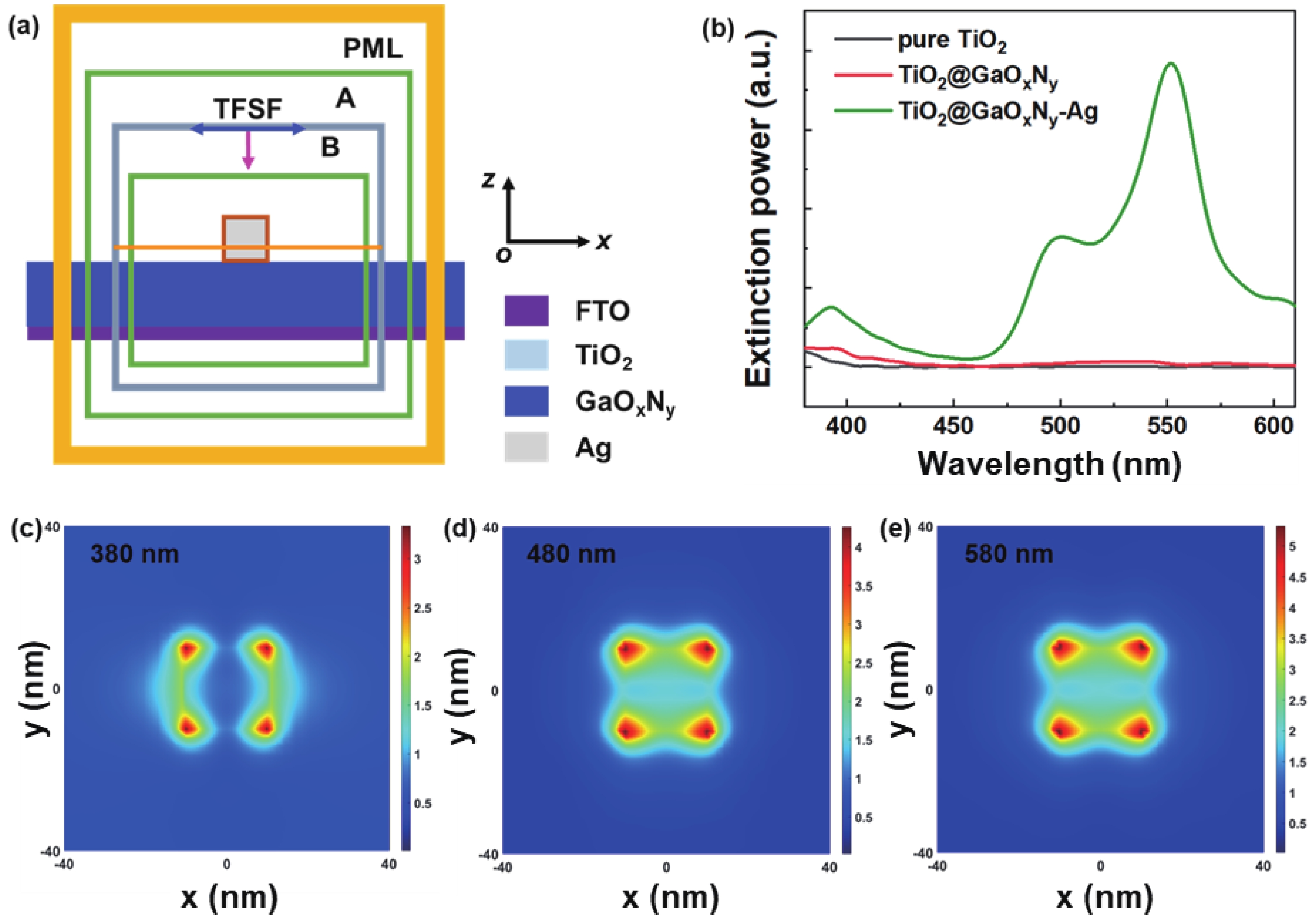
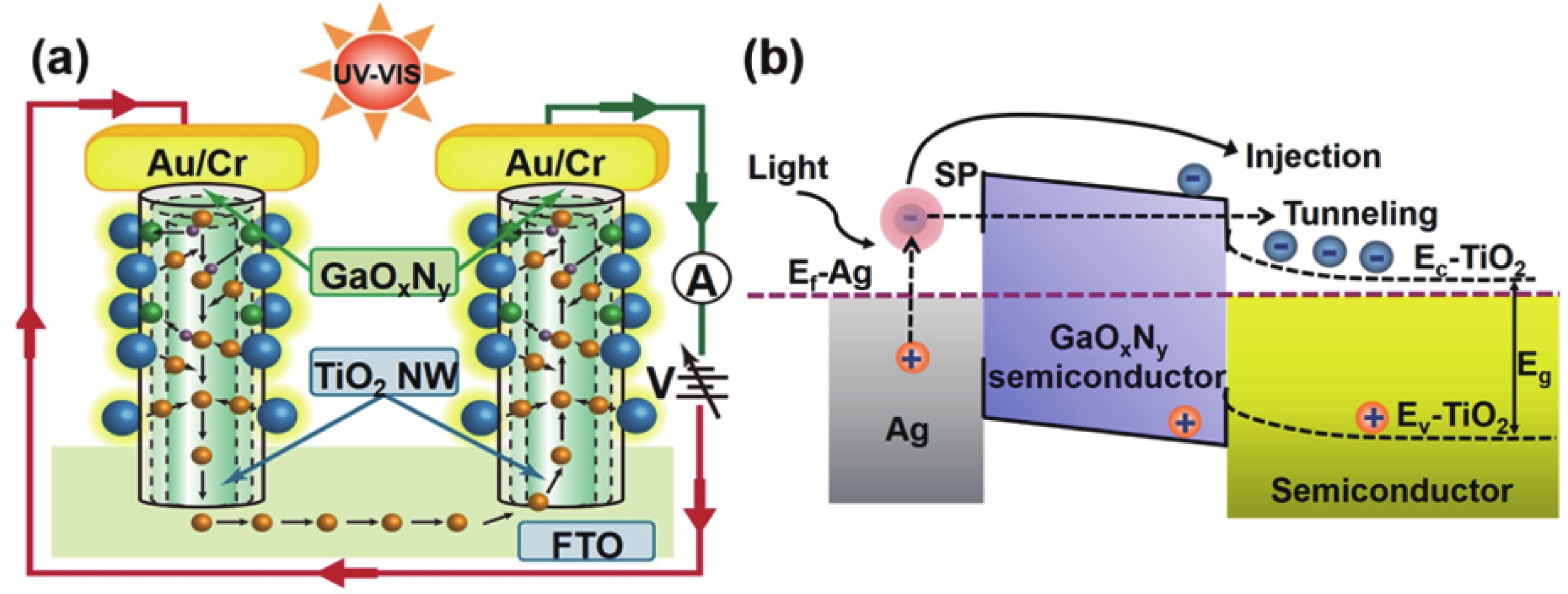
 DownLoad:


 Jiajia Tao:received the Ph.D. degree in School of Microelectronics, Fudan University, Shanghai, China. He is currently a senior engineer in the 50th Research Institute of China Electronics Technology Group Corporation, Shanghai, China. His main research interests include ALD Ga2O3-based photodetectors, low-dimensional material optoelectronic devices, and functional module design for Si-based chips
 Guang Zeng:is a Ph.D. candidate in School of Microelectronics, Fudan University, Shanghai, China. His main research interests include solar-blind photodetectors based on β-Ga2O3, waveguide-integrated low-dimensional material photodetectors, and low-dimensional material optoelectronic devices
 Hongliang Lu:is a professor and doctoral supervisor in the School of Microelectronics, Fudan University. His main research direction is new semiconductor materials and devices for the next generation of Integrated Circuit (IC) technology. In the meantime, he has published more than 200 papers in international academic journals and 20 domestic patents


