


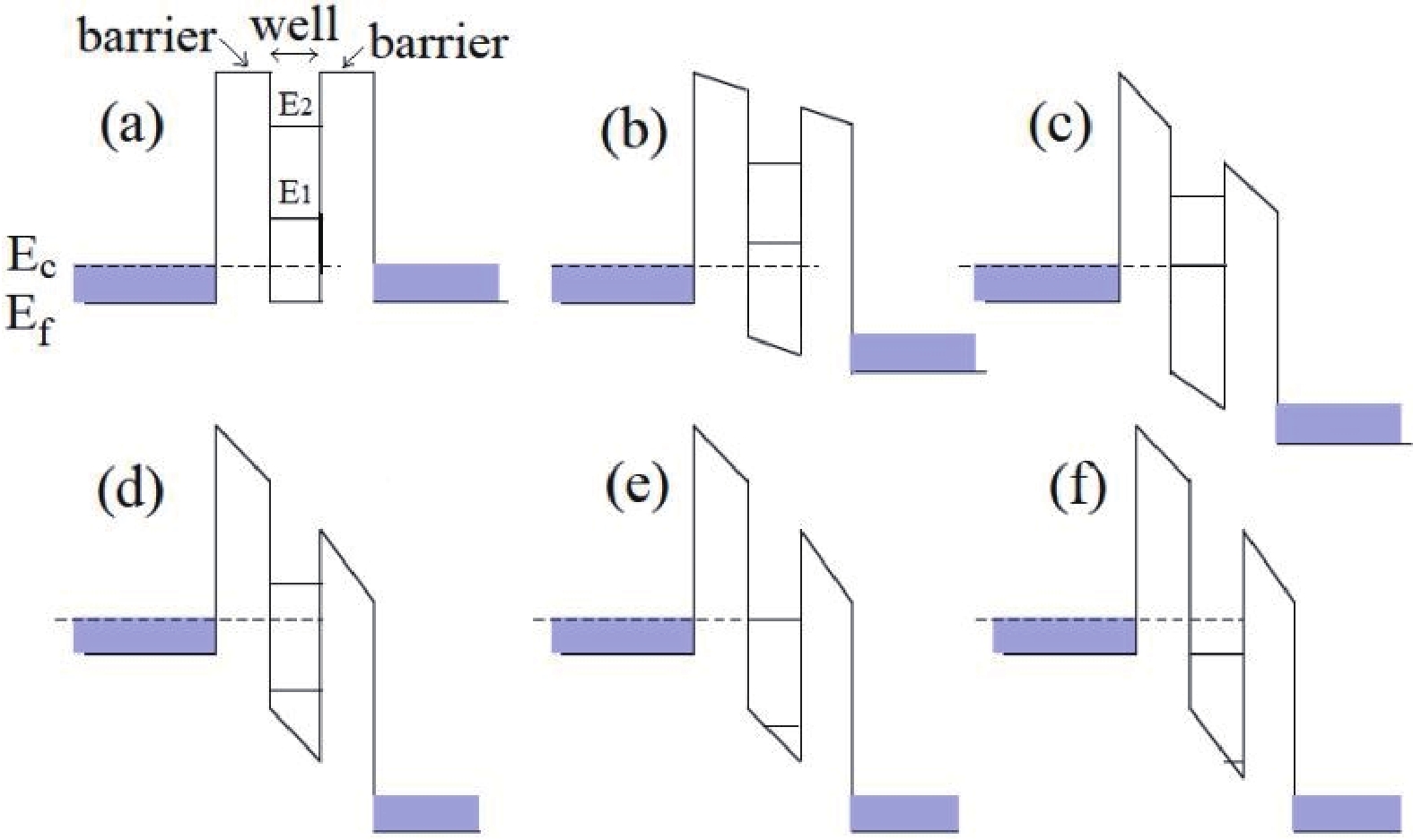
Fig. 1.
(Color online) Energy band diagram of a typical double-barrier RTD structure.
REVIEWS
Corresponding author: Swagata Samanta, swagata.s@srmap.edu.in
Abstract: This review article discusses the development of gallium arsenide (GaAs)-based resonant tunneling diodes (RTD) since the 1970s. To the best of my knowledge, this article is the first review of GaAs RTD technology which covers different epitaxial-structure design, fabrication techniques, and characterizations for various application areas. It is expected that the details presented here will help the readers to gain a perspective on the previous accomplishments, as well as have an outlook on the current trends and future developments in GaAs RTD research.
Key words: gallium arsenide, microfabrication, resonant tunneling devices
| [1] |
Esaki L, Tsu R. Superlattice and negative differential conductivity in semiconductors. IBM J Res Dev, 1970, 14, 61 doi: 10.1147/rd.141.0061
|
| [2] |
Tsu R, Esaki L. Tunneling in a finite superlattice. Appl Phys Lett, 1973, 22, 562 doi: 10.1063/1.1654509
|
| [3] |
Chang L L, Esaki L, Tsu R. Resonant tunneling in semiconductor double barriers. Appl Phys Lett, 1974, 24, 593 doi: 10.1063/1.1655067
|
| [4] |
Hall R N. Tunnel diodes. IRE Trans Electron Devices, 1960, 7, 1 doi: 10.1109/T-ED.1960.14584
|
| [5] |
Sommers H S. Tunnel diodes as high-frequency devices. Proc IRE, 1959, 47, 1201 doi: 10.1109/JRPROC.1959.287351
|
| [6] |
Sterzer F, Nelson D. Tunnel-diode microwave oscillators. Proc IRE, 1961, 49, 744 doi: 10.1109/JRPROC.1961.287845
|
| [7] |
Burrus C A. Gallium arsenide Esaki diodes for high-frequency applications. J Appl Phys, 1961, 32, 1031 doi: 10.1063/1.1736154
|
| [8] |
Greene J C, Sard E W. Experimental tunnel-diode mixer. Proc IRE, 1961, 49, 350
|
| [9] |
Robertson W J. A broadband hybrid coupled tunnel diode down converter. Proc IRE, 1960, 48, 2023
|
| [10] |
Reindel J. Tunnel diode circuits at nicrowave frequencies. 1961. Available: https://apps.dtic.mil/dtic/tr/fulltext/u2/269846.pdf
|
| [11] |
Bessho T, Hiyama Y, Niiyama H. Memory circuit using Esaki diode. Review of the Electrical Communication Laboratory, Tokyo, 1969, 17, 89
|
| [12] |
Roblin P, Rohdin H. High-speed heterostructure devices: From device concepts to circuit modeling. Cambridge: Cambridge University Press, 2002
|
| [13] |
Mizuta H, Tanoue T. The physics and applications of resonant tunnelling diodes. Cambridge: Cambridge University Press, 1995
|
| [14] |
Figueiredo J M L. Optoelectronic properties of resonant tunnelling diodes. Ph.D. Dissertation, University of Glasgow, 2000
|
| [15] |
Dobson P. Physics of semiconductor devices (2nd ed.). Phys Bull, 1982
|
| [16] |
Levinshtein M. Handbook series on semiconductor parameters: vol. 2 Ternary and quaternary III-V compounds. World Scientific, 1996
|
| [17] |
Wang Y, Zahid F, Zhu Y, et al. Publisher’s Note: Band offset of GaAs/AlxGa1–xAs heterojunctions from atomistic first principles [Appl. Phys. Lett. 102, 132109 (2013)]. Appl Phys Lett, 2013, 103, 049901 doi: 10.1063/1.4809584
|
| [18] |
Campbell A C, Kesan V P, Block T R, et al. Influence of MBE growth temperature on GaAs/AlAs resonant tunneling structures. J Electron Mater, 1989, 18, 585 doi: 10.1007/BF02657470
|
| [19] |
Nishiwaki T, Yamaguchi M, Sawaki N. AlGaAs/GaAs nano-hetero-epitaxy on a patterned GaAs substrate by MBE. AIP Conference Proceedings, Vienna (Austria), 2007, 893, 61 doi: 10.1063/1.2729770
|
| [20] |
Kapre R, Madhukar A, Kaviani K, et al. Realization and analysis of GaAs/AlAs/In0.1Ga0.9As based resonant tunneling diodes with high peak-to-valley ratios at room temperature. Appl Phys Lett, 1990, 56, 922 doi: 10.1063/1.102626
|
| [21] |
Koenig E T, Jogai B, Paulus M J, et al. Charge-quantization effects on current–voltage characteristics of AlGaAs/GaAs resonant tunneling diodes with spacer layers. J Appl Phys, 1990, 68, 3425 doi: 10.1063/1.346349
|
| [22] |
Kim S K, Kang T W, Kim T W. Electrical transport properties of AlAs/GaAs resonant tunneling diodes. Phys Status Solidi A, 1993, 140, K17 doi: 10.1002/pssa.2211400132
|
| [23] |
Schmidt T, Tewordt M, Haug R J, et al. Peak-to-valley ratio of small resonant-tunneling diodes with various barrier-thickness asymmetries. Appl Phys Lett, 1996, 68, 838 doi: 10.1063/1.116550
|
| [24] |
Tsuchiya M, Sakaki H. Dependence of resonant tunneling current on well widths in AlAs/GaAs/AlAs double barrier diode structures. Appl Phys Lett, 1986, 49, 88 doi: 10.1063/1.97360
|
| [25] |
Su B, Goldman V J, Cunningham J E. Single-electron tunneling in nanometer-scale double-barrier heterostructure devices. Phys Rev B, 1992, 46, 7644 doi: 10.1103/PhysRevB.46.7644
|
| [26] |
Goldman V J, Tsui D C, Cunningham J E. Observation of intrinsic bistability in resonant tunneling structures. Phys Rev Lett, 1987, 58, 1256 doi: 10.1103/PhysRevLett.58.1256
|
| [27] |
Wei T, Stapleton S. Effect of spacer layers on capacitance of resonant tunneling diodes. J Appl Phys, 1994, 76, 1287 doi: 10.1063/1.357788
|
| [28] |
Mehdi I, Mains R K, Haddad G I. Effect of spacer layer thickness on the static characteristics of resonant tunneling diodes. Appl Phys Lett, 1990, 57, 899 doi: 10.1063/1.103398
|
| [29] |
Singh M M, Siddiqui M J, Khan A B, et al. Effect of barriers length and doping concentration on GaAs/AlGaAs RTD. 2015 Annual IEEE India Conference (INDICON), 2016, 1 doi: 10.1109/INDICON.2015.7443753
|
| [30] |
Singh M M, Siddiqui M J, Khan A B, et al. Simulation study of I–V characteristics of RTD with variation in doping concentration. IMPACT-2013, 2013, 260 doi: 10.1109/MSPCT.2013.6782131
|
| [31] |
Wang J. Monolithic microwave/millimetre wave integrated circuit resonant tunnelling diode sources with around a milliwatt output power, Ph.D. Thesis, University of Glasgow, 2014
|
| [32] |
Md Zawawi M A, Missous M. Design and fabrication of low power GaAs/AlAs resonant tunneling diodes. Solid-State Electron, 2017, 138, 30 doi: 10.1016/j.sse.2017.09.004
|
| [33] |
Dultsev F N, Nenasheva L A. The effect of hydrogen as an additive in reactive ion etching of GaAs for obtaining polished surface. Appl Surf Sci, 2006, 253, 1287 doi: 10.1016/j.apsusc.2006.01.073
|
| [34] |
Wang J, Alharbi K, Khalid A, et al. Planar fabrication process development for mm-wave resonant tunneling diode (RTD) using BCB etch-back. 27th International Conference on Indium Phosphide and Related Materials, 2015
|
| [35] |
Ivey D G, Eicher S, Wingar S, et al. Performance of Pd–Ge based ohmic contacts to n-type GaAs. J Mater Sci Mater Electron, 1997, 8, 63 doi: 10.1023/A:1018557005117
|
| [36] |
Islam M S, McNally P J, Cameron D C, et al. Properties of Pd/Sn ohmic contacts on n-GaAs. J Mater Process Technol, 1998, 77, 42 doi: 10.1016/S0924-0136(97)00391-9
|
| [37] |
Kwak J S, Baik H K, Lee J L, et al. A low-resistance Pd/Ge/Ti/Au ohmic contact to a high-low doped GaAs field-effect transistor. Thin Solid Films, 1996, 290/291, 497 doi: 10.1016/S0040-6090(96)08967-5
|
| [38] |
Lim J W, Mun J K, Nam S, et al. PdGe-based ohmic contacts to high-low doped n-GaAs with and without undoped cap layer. J Phys D: Appl Phys, 2000, 33, 1611 doi: 10.1088/0022-3727/33/13/309
|
| [39] |
Lim J W, Mun J K, Kwak M H, et al. Performance of Pd/Ge/Au/Pd/Au ohmic contacts and its application to GaAs metal-semiconductor field-effect transistors. Solid-State Electron, 1999, 43, 1893 doi: 10.1016/S0038-1101(99)00149-5
|
| [40] |
Papageorgiou V. Integration of planar Gunn diodes and HEMTs for high-power MMIC oscillators. Ph.D. Thesis, University of Glasgow, 2014
|
| [41] |
Lin H C, Senanayake S, Cheng K Y, et al. Optimization of AuGe-Ni-Au ohmic contacts for GaAs MOSFETs. IEEE Trans Electron Devices, 2003, 50, 880 doi: 10.1109/TED.2003.812097
|
| [42] |
Aboelfotoh M O, Oktyabrsky S, Narayan J, et al. Electrical and microstructural characteristics of Ge/Cu ohmic contacts to n-type GaAs. J Mater Res, 1997, 12, 2325 doi: 10.1557/JMR.1997.0308
|
| [43] |
Erofeev E V, Loshchilov A G, Tomashevich A A, et al. Low resistance ohmic contacts to n+ -GaAs with refractory metal sidewall diffusion barrier. International J Civil Engg Technol, 2018, 9, 994
|
| [44] |
Oku T, Furumai M, Uchibori C J, et al. Formation of WSi-based ohmic contacts to n-type GaAs. Thin Solid Films, 1997, 300, 218 doi: 10.1016/S0040-6090(96)09511-9
|
| [45] |
Zhou J, Xia G Q, Li B H, et al. Electrical and structural properties of refractory metal multilayer Au/Ti/W/Ti ohmic contacts to n-GaAs. Jpn J Appl Phys, 2003, 42, 2609 doi: 10.1143/JJAP.42.2609
|
| [46] |
Davies D W, Morgan D V, Thomas H. Indium-based ohmic contacts to n-GaAs, fabricated using an ion-assisted deposition technique. Semicond Sci Technol, 1999, 14, 615 doi: 10.1088/0268-1242/14/7/305
|
| [47] |
Guan L H, Yusof A, Dolah A, et al. The etching of GaAs, AlGaAs and InGaAs in different chemicals in p-HEMT mesa layers. 2004 IEEE International Conference on Semiconductor Electronics, 2006, 1 doi: 10.1109/SMELEC.2004.1620919
|
| [48] |
Sioncke S, Brunco D P, Meuris M, et al. Etch rates of Ge, GaAs and InGaAs in acids, bases and peroxide based mixtures. ECS Trans, 2008, 16, 451 doi: 10.1149/1.2986802
|
| [49] |
Skriniarova J, Kovac J, Breza J, et al. Wet etching of InGaP and GaAs in HCl: H3PO4: H2O2. Sensors and Materials, 1998, 10, 213
|
| [50] |
Flemish J R, Jones K A. Selective wet etching of GaInP, GaAs, and InP in solutions of HCl, CH3COOH , and H2O2. J Electrochem Soc, 1993, 140, 844 doi: 10.1149/1.2056170
|
| [51] |
Noda T, Mitsuishi K, Mano T. Fabrication of submicron GaAs/AlAs double-barrier resonant tunneling diodes by wet etching with in droplets as mask. Jpn J Appl Phys, 2007, 46, L994 doi: 10.1143/JJAP.46.L994
|
| [52] |
Fobelets K, Vounckx R, Borghs G. A GaAs pressure sensor based on resonant tunnelling diodes. J Micromech Microeng, 1994, 4, 123 doi: 10.1088/0960-1317/4/3/005
|
| [53] |
Lee H J, Tse M S, Radhakrishnan K, et al. Selective wet etching of a heterostructure with citric acid-hydrogen peroxide solutions for pseudomorphic GaAs/AlxGa1–xAs/InyGa1–yAs heterojunction field effect transister fabrication. Mater Sci Eng B, 1995, 35, 230 doi: 10.1016/0921-5107(95)01414-4
|
| [54] |
Juang C. Selective etching of GaAs and Al0.30Ga0.70As with citric acid/hydrogen peroxide solutions. J Vac Sci Technol B, 1990, 8, 1122 doi: 10.1116/1.584928
|
| [55] |
Hays D C. Selective etching of compound semiconductors. Master of Science Thesis, University of Florida, 1999
|
| [56] |
Wang H L, Guo X, Shen G D. GaAs backside via-hole etching using ICP system. Sci China Ser E-Technol Sci, 2007, 50, 749 doi: 10.1007/s11431-007-0032-2
|
| [57] |
Rawal D, Agarwal V, Sharma H, et al. Dry etching of GaAs to fabricate via-hole grounds in monolithic microwave integrated circuits. Def Sci J, 2009, 59, 363 doi: 10.14429/dsj.59.1535
|
| [58] |
Vigneron P B, Joint F, Isac N, et al. Advanced and reliable GaAs/AlGaAs ICP-DRIE etching for optoelectronic, microelectronic and microsystem applications. Microelectron Eng, 2018, 202, 42 doi: 10.1016/j.mee.2018.09.001
|
| [59] |
Booker K, Mayon Y O, Jones C, et al. Deep, vertical etching for GaAs using inductively coupled plasma/reactive ion etching. J Vac Sci Technol B, 2020, 38, 012206 doi: 10.1116/1.5129184
|
| [60] |
Chang E Y, Van Hove J M, Pande K P. A selective dry-etch technique for GaAs MESFET gate recessing. IEEE Trans Electron Devices, 1988, 35, 1580 doi: 10.1109/16.7356
|
| [61] |
Lujan A S, Ramos A C S, Swart J W. Reactive ion etching of GaAs using SiCl4/Ar. Unicamp, Sau Paulo, Brazil, Available: https://www.ipen.br/biblioteca/cd/cbms/1997/SBMicro/ARTIGO34.PDF
|
| [62] |
Lee Y S, Upadhyaya K, Nordheden K J, et al. Selective reactive ion etching of GaAs/AlAs in BCl3/SF6 for gate recess. J Vac Sci Technol B, 2000, 18, 2505 doi: 10.1116/1.1288134
|
| [63] |
Liu H C, Sollner T C L G. High-frequency resonant-tunneling devices. In: Semiconductors and semimetals. Elsevier, 1994
|
| [64] |
Brown E R, Goodhue W D, Sollner T C L G. Fundamental oscillations up to 200 GHz in resonant tunneling diodes and new estimates of their maximum oscillation frequency from stationary-state tunneling theory. J Appl Phys, 1988, 64, 1519 doi: 10.1063/1.341827
|
| [65] |
Brown E R, Sollner T C L G, Goodhue W D, et al. Millimeter-band oscillations based on resonant tunneling in a double-barrier diode at room temperature. Appl Phys Lett, 1987, 50, 83 doi: 10.1063/1.97826
|
| [66] |
Brown E R, Sollner T C L G, Parker C D, et al. Oscillations up to 420 GHz in GaAs/AlAs resonant tunneling diodes. Appl Phys Lett, 1989, 55, 1777 doi: 10.1063/1.102190
|
| [67] |
Bouregba R, Vanbesien O, Saint de Pol L, et al. Al0.3Ga0.7As-GaAs microwave resonant tunneling oscillator. Ann Télécommun, 1990, 45, 184
|
| [68] |
Tsao A. AlAs/GaAs Double barrier resonant tunneling diodes. Ph.D. Thesis, Chapter 4, University of Texas at Austin, 1993, 45
|
| [69] |
Bouregba R, Vanbesien O, Mounaix P, et al. Resonant tunneling diodes as sources for millimeter and submillimeter wavelengths. IEEE Trans Microwave Theory Techn, 1993, 41, 2025 doi: 10.1109/22.273430
|
| [70] |
Wolak E, Özbay E, Park B G, et al. The design of GaAs/AlAs resonant tunneling diodes with peak current densities over 2 × 10⁵A cm–2. J Appl Phys, 1991, 69, 3345 doi: 10.1063/1.348563
|
| [71] |
Wei T, Stapleton S, Berolo O. Capacitance and hysteresis study of AlAs/GaAs resonant tunneling diode with asymmetric spacer layers. J Appl Phys, 1995, 77, 4071 doi: 10.1063/1.359490
|
| [72] |
Huang Y L, Ma L, Yang F H, et al. Resonant tunnelling diodes and high electron mobility transistors integrated on GaAs substrates. Chin Phys Lett, 2006, 23, 697 doi: 10.1088/0256-307X/23/3/048
|
| [73] |
Van Hoof C, Genoe J, Mertens R, et al. Electroluminescence from bipolar resonant tunneling diodes. Appl Phys Lett, 1992, 60, 77 doi: 10.1063/1.107380
|
| [74] |
Cheng P, Harris J S Jr. Improved design of AlAs/GaAs resonant tunneling diodes. Appl Phys Lett, 1990, 56, 1676 doi: 10.1063/1.103114
|
| [75] |
Huang C I, Paulus M J, Bozada C A, et al. AlGaAs/GaAs double barrier diodes with high peak-to-valley current ratio. Appl Phys Lett, 1987, 51, 121 doi: 10.1063/1.98588
|
| [76] |
Forster A, Lange J, Gerthsen D, et al. The effect of growth temperature on AlAs/GaAs resonant tunnelling diodes. J Phys D: Appl Phys, 1994, 27, 175 doi: 10.1088/0022-3727/27/1/028
|
| [77] |
Alkeev N V, Averin S V, Dorofeev A A, et al. GaAs/AlAs resonant-tunneling diode for subharmonic mixers. Russ Microelectron, 2010, 39, 331 doi: 10.1134/S1063739710050057
|
| [78] |
Kan S C, Wu S, Sanders S, et al. Optically controlled resonant tunneling in a double-barrier diode. J Appl Phys, 1991, 69, 3384 doi: 10.1063/1.348515
|
| [79] |
Yang L, Draving S D, Mars D E, et al. A 50 GHz broad-band monolithic GaAs/AlAs resonant tunneling diode trigger circuit. IEEE J Solid-State Circuits, 1994, 29, 585 doi: 10.1109/4.284711
|
| [80] |
Leung C S Y, Wintreert-Fouquet M, Skellern D J. Switching time measurements of GaAs/AlAs and InGaAs/AlAs resonant tunnelling diodes. 1998 Conference on Optoelectronic and Microelectronic Materials and Devices, Proceedings (Cat. No. 98EX140), 2002, 144 doi: 10.1109/COMMAD.1998.791604
|
| [81] |
Kanaya H, Sogabe R, Maekawa T, et al. Fundamental oscillation up to 1.42 THz in resonant tunneling diodes by optimized collector spacer thickness. J Infrared, Millimeter and Terahertz Waves, 2014, 35, 425 doi: 10.1007/s10762-014-0058-z
|
| [82] |
Izumi R, Suzuki S, Asada M. 1.98 THz resonant-tunneling-diode oscillator with reduced conduction loss by thick antenna electrode. 42nd International Conference on Infrared, Millimeter, and Terahertz Waves (IRMMW-THz), 2017, 1 doi: 10.1109/IRMMW-THz.2017.8066877
|
| [83] |
Sellai A, Raven M S, Steenson D P, et al. Double-barrier resonant tunnelling diode three-state logic. Electron Lett, 1990, 26, 61 doi: 10.1049/el:19900040
|
| [84] |
Sollner T C L G, Tannenwald P E, Peck D D, et al. Quantum well oscillators. Appl Phys Lett, 1984, 45, 1319 doi: 10.1063/1.95134
|
| [85] |
Pfenning A, Hartmann F, Langer F B, et al. Cavity-enhanced resonant tunneling photodetector at telecommunication wavelengths. Appl Phys Lett, 2014, 104, 101109 doi: 10.1063/1.4868429
|
| [86] |
Pfenning A, Jurkat J, Naranjo A, et al. Resonant tunneling diode photon number resolving single-photon detectors. Proc SPIE 11128, Infrared Remote Sensing and Instrumentation XXVII, 2019, 1112808 doi: 10.1117/12.2529929
|
| [87] |
Watson S, Zhang W K, Tavares J, et al. Resonant tunneling diode photodetectors for optical communications. Microw Opt Technol Lett, 2019, 61, 1121 doi: 10.1002/mop.31689
|
| [88] |
Mutamba K, Flath M, Sigurdardottir A, et al. A GaAs pressure sensor with frequency output based on resonant tunneling diodes. IEEE Trans Instrum Meas, 1999, 48, 1333 doi: 10.1109/19.816157
|
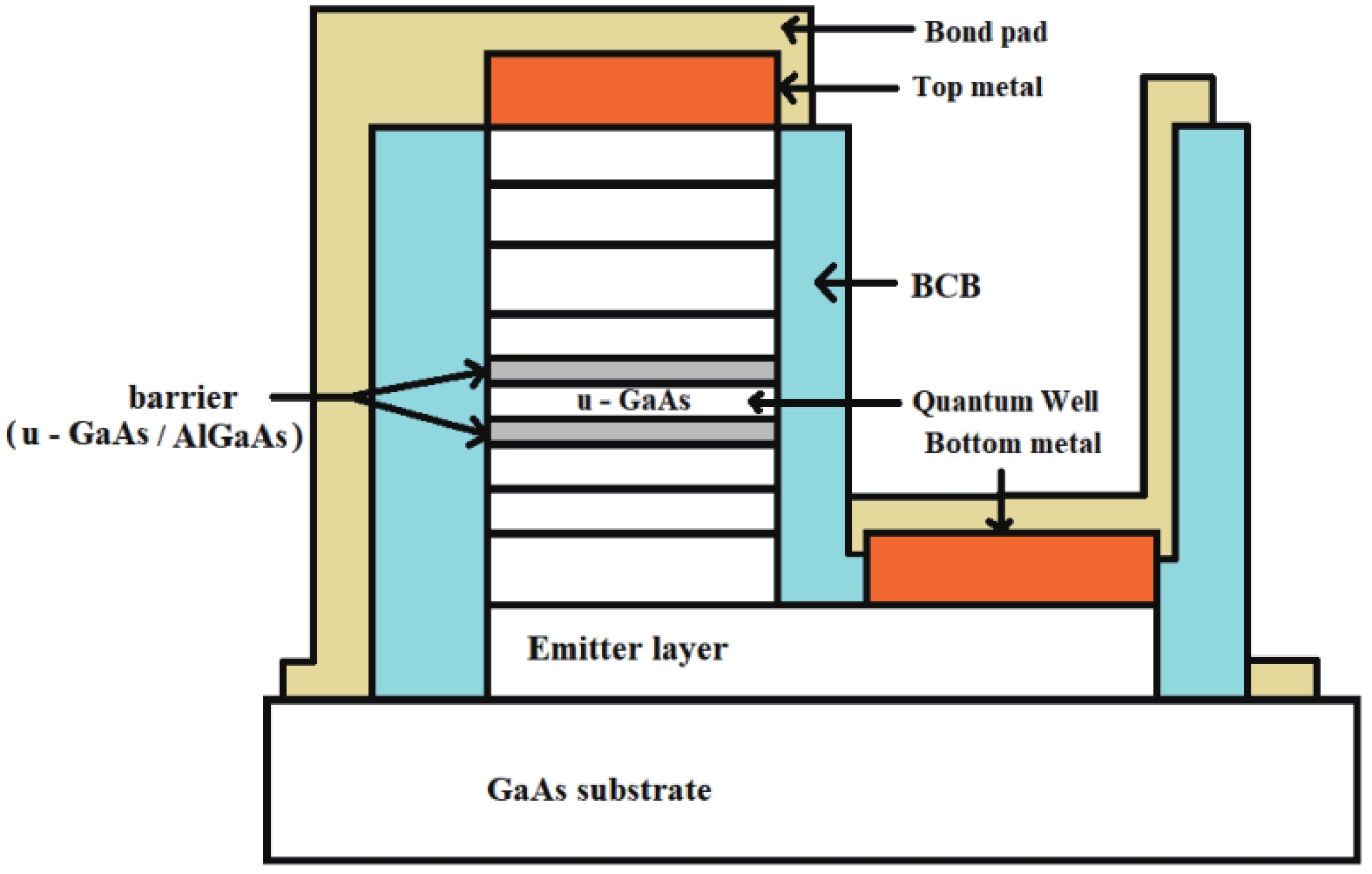
Table 1. Material properties for different semiconductors at room temperature.
| Material | Lattice constant (Ǻ) |
Electron mobility (cm2/(V·s)) |
Relative dielectric constant |
Energy bandgap (eV) |
Electron effective mass (m0) |
| Si | 5.43095 | 1500 | 11.9 | 1.12 (indirect) | l1: 0.98 t: 0.19 |
| Ge | 5.64613 | 3900 | 16.0 | 0.66 (indirect) | l: 1.64 t: 0.082 |
| GaAs | 5.6533 | 8500 | 13.1 | 1.424 (direct) | 0.063 |
| AlAs | 5.6605 | 180 | 10.1 | 2.36 (indirect) | 0.11 |
| AlxGa1-xAs | 5.6533 + 0.0078 x |
8 × 10³ – 2.2 × 10⁴x + 104x2 (for 0 < x < 0.45); –255 + 1160x – 720x2 (for 0.45 < x < 1) |
11.96 (when x = 0.33) |
1.42–2.36 (direct when x < 0.4) |
0.063 + 0.083x (for 0 < x < 0.45) |
| GaP | 5.4512 | 110 | 11.1 | 2.26 (indirect) | 0.82 |
| GaN | a = 3.189 c = 5.182 |
400 | 10.4 | 3.44 (direct) | 0.27 |
| InP | 5.8686 | 4600 | 12.6 | 1.35 (direct) | 0.077 |
| 1where, electron rest mass (m0) = 9.11 × 10⁻³¹ kg; l: longitudinal; t: transverse. | |||||
 DownLoad: CSV
Table 2. Ohmic contact formation on GaAs substrate.
| Metal scheme | Deposition method | Anneal temperature (°C) | Anneal time (s) | Specific contact resistance (Ω·cm2) | Ref. |
| Pd/Ge/Pd | EB-PVD | 430 | 15 | 3.2 × 10⁻⁴ | [35] |
| Pd/Ge/Ti/ Pt | EB-PVD | 430 | 15 | 8 × 10⁻⁷ | [35] |
| Pd/Ge/Pd/Ti/Au | EB-PVD | 415 | 15 | 4.3 × 10⁻⁷ | [35] |
| Pd/Sn | Resistance-heating evaporation | 360 | 1800 | 3.26 × 10⁻⁵ | [36] |
| Pd/Ge/ Ti/Au | EB-PVD | 340 | 20 | 2.8 × 10⁻⁶ | [37] |
| Pd/Ge/ Ti/Pt | EB-PVD | 380–450 | 20 | (2.4–5.3) × 10–6 | [38] |
| Pd/Ge/Au/Pd/Au | EB-PVD | 400 | 30 | 2 × 10⁻⁶ | [39] |
| Pd/Ge/Au/Pd/Au | EB-PVD | 320 initially, then 400 | 20, then 60 | 2 × 10⁻⁶ | [40] |
| Au/Ge/Ni/Au | EB-PVD | 400 | 60 | 5.6 × 10⁻⁶ | [41] |
| Ge/Cu | EB-PVD | 400 | 1800 | 7 × 10⁻⁷ | [42] |
| Ge/Au/Ni/Ta/Au | Magnetron sputtering | 450 | – | 7 × 10⁻⁷ | [43] |
| WSi/Cu | RF sputtering | 400 | 5 | 6.3 × 10⁻⁶ | [44] |
| Au/Ti/W/Ti | Sputtering and EB-PVD | 400 | 30 | 5.5 × 10⁻⁶ | [45] |
| In | IAD | 375 | 60 | 3 × 10⁻⁶ | [46] |
| where, EB-PVD: electron beam physical vapor deposition; RF: radio frequency; resistance-heating evaporation: resistive evaporation; IAD: ion-assisted deposition. | |||||
DownLoad: CSV
Table 3. Wet etching solution for GaAs material around room temperature.
| Etching solution | Etchant ratio | Temperature (°C) | Etch rate (nm/min) | Ref. |
| NH4OH : H2O2 : H2O | 1 : 1 : 25 | 25 | 924 | [47] |
| 1 : 1 : 50 | 594 | |||
| 1 : 2 : 50 | 861 | |||
| 2 : 1 : 50 | 993 | |||
| 1 : 1 : 250 | 177 | |||
| 1 : 1 : 500 | 54 | |||
| 40 : 4 : 1 | Room temp. | 202.6 | [48] | |
| 40 : 10 : 0 | 509.1 | |||
| 40 : 20 : 0 | 1385 | |||
| 1 : 1 : 5 | 1890 | |||
| 1 : 10 : 500 | 25 | |||
| 10 : 1 : 500 | 18 | |||
| 1 : 10 : 5000 | 6.1 | |||
| 1 : 1 : 5000 | 1.65 | |||
| 1 : 10 : 3000 | 12 | |||
| HCl : H3PO4 : H2O | 1 : 10 : 1 | 20 | 10 | [49] |
| HCl : CH3COOH : H2O | 1 : 10 : 1 | 20 | 60 | [49] |
| HCl : CH3COOH : H2O2 | 1 : 20 : 0 | 20 | 10 | [50] |
| 1 : 20 : 1 | 50 | |||
| 1 : 20 : 2 | 120 | |||
| 1 : 20 : 3 | 270 | |||
| 1 : 2 : 1 | 440 | |||
| 1 : 5 : 1 | 250 | |||
| 1 : 10 : 1 | 120 | |||
| 1 : 20 : 1 | 50 | |||
| 1 : 30 : 1 | 30 | |||
| 1 : 40 : 1 | 15 | |||
| H3PO4 : H2O2 : H2O | 3 : 1 : 50 | Room temp. | 60 | [32] |
| 3 : 1 : 75 | Room temp. | 72 | [51] | |
| 1 : 1 : 25 | 25 | 259.8 | [47] | |
| 1 : 1 : 50 | 130.8 | |||
| 1 : 2 : 50 | 244.8 | |||
| 2 : 1 : 50 | 129 | |||
| 1 : 1 : 250 | 40.8 | |||
| 1 : 1 : 500 | 7.8 | |||
| H3PO4 : HNO3 | 3 : 1 | Room temp. | 1125 | [48] |
| H2SO4 : H2O2 | 4 : 1 | Room temp. | 1073 | [48] |
| H2SO4 : H2O2 : H2O | 4 : 3 : 3 | Room temp. | 9000 | [52] |
| 1 : 1 : 25 | 25 | 234 | [47] | |
| 1 : 1 : 50 | 90.6 | |||
| 1 : 2 : 50 | 202.8 | |||
| 2 : 1 : 50 | 184.8 | |||
| 1 : 1 : 250 | 27 | |||
| 1 : 1 : 500 | 27.6 | |||
| C6H8O7 : H2O2 | 2 : 1 | 20 | 30 | [53] |
| 3 : 1 | 45 | |||
| 4 : 1 | 45 | |||
| 5 : 1 | 42 | |||
| 7 : 1 | 33 | |||
| 10 : 1 | 21 | |||
| 1 : 1 | 18 | 5 | [54] | |
| 1 : 3 | 7 | |||
| 1 : 5 | 200 | |||
| 1 : 10 | 210 | |||
| 1 : 15 | 150 | |||
| 1 : 25 | 90 | |||
| 1 : 1 | 21 | 5.8 | [55] | |
| 2 : 1 | 570 | |||
| HCl : HNO3 | 3 : 1 | Room temp. | 477 | [48] |
| HCl : HNO3 : H2O | 1 : 1 : 1 | Room temp. | 2277 | [48] |
| HCl : H2O2 : H2O | 1 : 10 : 500 | Room temp. | 9.27 | [48] |
| 80 : 4 : 1 | 185 | |||
| 1 : 10 : 5000 | 8.21 | |||
| HF : HNO3 : H2O | 1 : 1 : 1 | Room temp. | 122693 | [48] |
DownLoad: CSV
Table 4. Dry etching details for GaAs material.
| Inductively coupled plasma etching | ||||||
| Gas system | Flow rate (sccm) |
RF power (W) |
ICP power (W) |
Chamber pressure (mTorr) |
Etch rate (μm/min) |
Ref. |
| BCl3/Cl2 | 30/80 | 80 | 600 | 10 | 2.6 | [56] |
| 800 | 4.5 | |||||
| 1000 | 5.4 | |||||
| 1200 | 6.2 | |||||
| 1500 | 6.4 | |||||
| 600 | 5 | 3.2 | ||||
| 10 | 2.8 | |||||
| 15 | 1.8 | |||||
| 20 | 1.2 | |||||
| 150 | 10 | 3.6 | ||||
| 200 | 4.0 | |||||
| 300 | 4.4 | |||||
| BCl3/Cl2 | 3 : 4 (ratio) | 90 | 950 | 40 | ~4.0 | [57] |
| BCl3/Cl2 | 4 : 1 | RF : ICP = 1 : 8 | 10 | 3.64 | [58] | |
| 2 : 1 | 3.6 | |||||
| 2.5 : 1 | 2.38 | |||||
| 6 : 1 | 2.37 | |||||
| 8 : 1 | 2.1 | |||||
| BCl3/Cl2/Ar | 4 : 1 : 5 | RF : ICP = 1 : 8 | 10 | 2.38 | [58] | |
| 2.5 : 1 : 5 | 2.13 | |||||
| 6 : 1 : 5 | 2.0 | |||||
| BCl3/Cl2/Ar/N2 | 6 : 1 : 5 : 2 | RF : ICP = 1 : 8 | 10 | 3.84 | [58] | |
| 6 : 1 : 5 : 2.5 | 4.0 | |||||
| 6 : 1 : 5 : 3 | 4.0 | |||||
| 3 : 1 : 5 : 3 | 2.5 | |||||
| 20 : 1 : 5 : 3 | 1.8 | |||||
| 5 | 1.14 | |||||
| 20 | 2.36 | |||||
| 25 | 3.6 | |||||
| 30 | 3.7 | |||||
| 20 : 1:5 : 5 | 30 | 5.56 | ||||
| 20 | 4.1 | |||||
| 20 : 1 : 10 : 3 | 20 | 2.8 | ||||
| 20 : 1 : 20 : 3 | 3.0 | |||||
| 20 : 1 : 30 : 3 | 2.5 | |||||
| 20 : 1 : 50 : 3 | 2.23 | |||||
| BCl3/Cl2/ N2 |
20 : 1 : 3 | RF : ICP = 1 : 8 | 10 | 1.92 | [58] | |
| Cl2/Ar | 13/20 | 80 | 250 | 7.5 | 1.37 | [59] |
| 150 | 1.6 | |||||
| 200 | 1.82 | |||||
| Cl2/Ar/ SiCl4 |
13/20/5 | 150 | 250 | 7.5 | 1.65 | |
| Reactive ion etching | ||||||
| Gas system | Flow rate (sccm) | RF power (W) | Chamber pressure (mTorr) | Etch rate (μm/min) | Ref. | |
| CCl4/CCl2F2 | 1/5 | 200 | 40 | 1.3 | [57] | |
| CCl2F2/He | 10/15 | 85 | 10 | 0.2 | [60] | |
| 20 | 0.5 | |||||
| 30 | 0.7 | |||||
| 40 | 1.05 | |||||
| 50 | 1.3 | |||||
| 60 | 1.4 | |||||
| SiCl4/Ar | 5/10 | 20 | 30 | 0.75 | [61] | |
| 30 | 1.25 | |||||
| 50 | 1.25 | |||||
| 30 | 50 | 1.5 | ||||
| 80 | 2.5 | |||||
| SF6/(BCl3 + SF6) | 1 : 5 | 150 | 50 | 1.8 | [62] | |
| 2 : 5 | 4.2 | |||||
| 11 : 20 | 5.5 | |||||
| 3 : 5 | 2.7 | |||||
| 4 : 5 | 4.5 | |||||
| CCl2F2/Ar | 1 : 10 | 200 | 200 | 0.32 | [33] | |
| 300 | 0.23 | |||||
| 400 | 0.15 | |||||
| 500 | 0.08 | |||||
| 600 | 0.15 | |||||
DownLoad: CSV
Table 5. Performance of GaAs-based RTDs at room temperature.
| Material system | PVCR | Jp (kA/cm2) | Mesa size | Ref. | |
| Barrier (nm) | Well (nm) | ||||
| AlAs (1.7) | GaAs (4.5) | 3.5 | 40 | − | [64] |
| Al0.3Ga0.7As (3.0) | GaAs (4.5) | 1.3 | 12 | − | [65] |
| AlAs (2.5) | GaAs (4.5) | 1.7 | 8 | − | |
| AlAs (1.5) | GaAs (4.5) | 3.5 | 40 | − | |
| AlAs (1.1) | GaAs (4.5) | 1.5 | 150 | Φ = 4 μm |
[66] |
| Al0.3Ga0.7As (5.0) | GaAs (5.0) | 1.8 | 30 | 177 μm2 (Φ = 15 μm) |
[67] |
| AlAs (1.7) | GaAs (5.0) | 4.1 ± 0.1 | 48.8 ± 3.8 | − | [68] |
| 3.8 ± 0.2 | 52.2 ± 2.2 | − | |||
| AlAs (1.7) | GaAs (4.5) | 2.0 | 160 | Φ = 3.5 μm |
[69] |
| AlAs (1.4) | GaAs (5.1) | 1.8 | 250 ± 20 | (1−3) × 5 μm2 |
[70] |
| AlAs (1.7) | GaAs (4.5) | 2.0 | 140 ± 10 | ||
| AlAs (1.4) | GaAs (4.5) | 1.7 | 200 ± 20 | ||
| AlAs (1.7) | GaAs (4.5) | 5.0 | 35 | 49 | [71] |
| AlAs (1.7) | GaAs (5.0) | 4.8 | 8.3 | 36 | [72] |
| AlAs (4.0) | GaAs (5.5) | 1.45 | − | 900 | [73] |
| AlAs (2.0) | GaAs (5.0) | 4.1 | 13.3 | 49 | [74] |
| 5.0 | 14.7 | ||||
| Al0.42Ga0.58As (5.0) | GaAs (5.0) | 3.9 | 0.61 | 520 | [75] |
| Al0.42Ga0.58As (1.7) | GaAs (5.0) | 5.35 | 40 | >16 | [76] |
| AlAs (1.7) | GaAs (4.0) | 2.9 | 6 | 100 | [77] |
| AlAs (4.0) | GaAs (4.7) | 2.9 | 2 | 2500 | [78] |
| 1.7 | 1.53 | 7500 | |||
| AlAs (1.7) | GaAs (4.5) | 3.5 | 100 | 12 | [79] |
| AlAs (1.96) | GaAs (5.0) | 4.0 | 20 | 75 | [80] |
| AlAs (1.7) | GaAs (6.5) | 3.27 | 14.8 | 16 | [32] |
| 3.44 | 15.93 | 25 | |||
| 3.38 | 14.8 | 36 | |||
DownLoad: CSV
Table 6. Applications of GaAs-based RTDs.
| RTD as oscillator | |||||
| Material system | Operation frequency (GHz) | Temperature (K) | Output power (μW) | Ref. | |
| GaAs/AlGaAs | 18 | 200 | 0.5 | [84] | |
| GaAs/AlAs | 200 | 300 | 20 | [64] | |
| 60 | 60 | ||||
| 3 | 100 | ||||
| 0.2 | 200 |
||||
| GaAs/AlAs | 56 | 300 | 60 | [65] | |
| 87 | 18 |
||||
| GaAs/AlAs | 3 | 300 | 150 | [66] | |
| 12 | 150 | ||||
| 50 | 50 | ||||
| 100 | 25 | ||||
| 220 | 2 | ||||
| 350 | 0.2 | ||||
| 420 |
0.2 | ||||
| GaAs/AlGaAs | 2 to 12 | 300 | − | [67] | |
| GaAs/AlAs | 38.6 | 300 | 36 | [69] | |
| 110 | 12 | ||||
| RTD as photodetector/light sensor and in single photon detection | |||||
| Device scheme | Wavelength (μm) | Voltage (V) | Absorption (%) | Sensitivity (kA/W) | Ref. |
| RTD with absorption layer | 1.3 | 3.0 | − | 0.966 | [85] |
| RTD integrated into DBR cavity | 1.29 | 4.0 | 18.3 | 31.2 | [86] |
| RTD integrated into DBR cavity | 0.94 | − | 90 | − | [87] |
| Waveguide-integrated RTD | 0.94 | − | > 90 (max 99) | − | [87] |
| RTD as pressure sensor | |||||
| Material system | Frequency (kHz) | Sensitivity (kHz/MPa) | Ref. | ||
| GaAs/AlGaAs | 113 | 0.8 | [88] | ||
| RTD as switch | |||||
| Material system | Switching time (ps) | Voltage swing (mV) | Ref. | ||
| GaAs/AlAs | 20 | 60 | [80] | ||
| RTD as subharmonic mixer | |||||
| Material system | Threshold voltage for resonant tunneling (V) |
Temperature (K) |
Local oscillation power (dBm) |
Conversion loss (dB) |
Ref. |
| GaAs/AlAs | 0.75 | Room temp. | 12 | 11 | [77] |
| RTD in triggering | |||||
| Material system | Frequency range (GHz) | Time jitter (ps∙rms) | Bandwidth (GHz) | Ref. | |
| GaAs/AlAs | 5 to 50 | <1 | 60 | [79] | |
DownLoad: CSV
| [1] |
Esaki L, Tsu R. Superlattice and negative differential conductivity in semiconductors. IBM J Res Dev, 1970, 14, 61 doi: 10.1147/rd.141.0061
|
| [2] |
Tsu R, Esaki L. Tunneling in a finite superlattice. Appl Phys Lett, 1973, 22, 562 doi: 10.1063/1.1654509
|
| [3] |
Chang L L, Esaki L, Tsu R. Resonant tunneling in semiconductor double barriers. Appl Phys Lett, 1974, 24, 593 doi: 10.1063/1.1655067
|
| [4] |
Hall R N. Tunnel diodes. IRE Trans Electron Devices, 1960, 7, 1 doi: 10.1109/T-ED.1960.14584
|
| [5] |
Sommers H S. Tunnel diodes as high-frequency devices. Proc IRE, 1959, 47, 1201 doi: 10.1109/JRPROC.1959.287351
|
| [6] |
Sterzer F, Nelson D. Tunnel-diode microwave oscillators. Proc IRE, 1961, 49, 744 doi: 10.1109/JRPROC.1961.287845
|
| [7] |
Burrus C A. Gallium arsenide Esaki diodes for high-frequency applications. J Appl Phys, 1961, 32, 1031 doi: 10.1063/1.1736154
|
| [8] |
Greene J C, Sard E W. Experimental tunnel-diode mixer. Proc IRE, 1961, 49, 350
|
| [9] |
Robertson W J. A broadband hybrid coupled tunnel diode down converter. Proc IRE, 1960, 48, 2023
|
| [10] |
Reindel J. Tunnel diode circuits at nicrowave frequencies. 1961. Available: https://apps.dtic.mil/dtic/tr/fulltext/u2/269846.pdf
|
| [11] |
Bessho T, Hiyama Y, Niiyama H. Memory circuit using Esaki diode. Review of the Electrical Communication Laboratory, Tokyo, 1969, 17, 89
|
| [12] |
Roblin P, Rohdin H. High-speed heterostructure devices: From device concepts to circuit modeling. Cambridge: Cambridge University Press, 2002
|
| [13] |
Mizuta H, Tanoue T. The physics and applications of resonant tunnelling diodes. Cambridge: Cambridge University Press, 1995
|
| [14] |
Figueiredo J M L. Optoelectronic properties of resonant tunnelling diodes. Ph.D. Dissertation, University of Glasgow, 2000
|
| [15] |
Dobson P. Physics of semiconductor devices (2nd ed.). Phys Bull, 1982
|
| [16] |
Levinshtein M. Handbook series on semiconductor parameters: vol. 2 Ternary and quaternary III-V compounds. World Scientific, 1996
|
| [17] |
Wang Y, Zahid F, Zhu Y, et al. Publisher’s Note: Band offset of GaAs/AlxGa1–xAs heterojunctions from atomistic first principles [Appl. Phys. Lett. 102, 132109 (2013)]. Appl Phys Lett, 2013, 103, 049901 doi: 10.1063/1.4809584
|
| [18] |
Campbell A C, Kesan V P, Block T R, et al. Influence of MBE growth temperature on GaAs/AlAs resonant tunneling structures. J Electron Mater, 1989, 18, 585 doi: 10.1007/BF02657470
|
| [19] |
Nishiwaki T, Yamaguchi M, Sawaki N. AlGaAs/GaAs nano-hetero-epitaxy on a patterned GaAs substrate by MBE. AIP Conference Proceedings, Vienna (Austria), 2007, 893, 61 doi: 10.1063/1.2729770
|
| [20] |
Kapre R, Madhukar A, Kaviani K, et al. Realization and analysis of GaAs/AlAs/In0.1Ga0.9As based resonant tunneling diodes with high peak-to-valley ratios at room temperature. Appl Phys Lett, 1990, 56, 922 doi: 10.1063/1.102626
|
| [21] |
Koenig E T, Jogai B, Paulus M J, et al. Charge-quantization effects on current–voltage characteristics of AlGaAs/GaAs resonant tunneling diodes with spacer layers. J Appl Phys, 1990, 68, 3425 doi: 10.1063/1.346349
|
| [22] |
Kim S K, Kang T W, Kim T W. Electrical transport properties of AlAs/GaAs resonant tunneling diodes. Phys Status Solidi A, 1993, 140, K17 doi: 10.1002/pssa.2211400132
|
| [23] |
Schmidt T, Tewordt M, Haug R J, et al. Peak-to-valley ratio of small resonant-tunneling diodes with various barrier-thickness asymmetries. Appl Phys Lett, 1996, 68, 838 doi: 10.1063/1.116550
|
| [24] |
Tsuchiya M, Sakaki H. Dependence of resonant tunneling current on well widths in AlAs/GaAs/AlAs double barrier diode structures. Appl Phys Lett, 1986, 49, 88 doi: 10.1063/1.97360
|
| [25] |
Su B, Goldman V J, Cunningham J E. Single-electron tunneling in nanometer-scale double-barrier heterostructure devices. Phys Rev B, 1992, 46, 7644 doi: 10.1103/PhysRevB.46.7644
|
| [26] |
Goldman V J, Tsui D C, Cunningham J E. Observation of intrinsic bistability in resonant tunneling structures. Phys Rev Lett, 1987, 58, 1256 doi: 10.1103/PhysRevLett.58.1256
|
| [27] |
Wei T, Stapleton S. Effect of spacer layers on capacitance of resonant tunneling diodes. J Appl Phys, 1994, 76, 1287 doi: 10.1063/1.357788
|
| [28] |
Mehdi I, Mains R K, Haddad G I. Effect of spacer layer thickness on the static characteristics of resonant tunneling diodes. Appl Phys Lett, 1990, 57, 899 doi: 10.1063/1.103398
|
| [29] |
Singh M M, Siddiqui M J, Khan A B, et al. Effect of barriers length and doping concentration on GaAs/AlGaAs RTD. 2015 Annual IEEE India Conference (INDICON), 2016, 1 doi: 10.1109/INDICON.2015.7443753
|
| [30] |
Singh M M, Siddiqui M J, Khan A B, et al. Simulation study of I–V characteristics of RTD with variation in doping concentration. IMPACT-2013, 2013, 260 doi: 10.1109/MSPCT.2013.6782131
|
| [31] |
Wang J. Monolithic microwave/millimetre wave integrated circuit resonant tunnelling diode sources with around a milliwatt output power, Ph.D. Thesis, University of Glasgow, 2014
|
| [32] |
Md Zawawi M A, Missous M. Design and fabrication of low power GaAs/AlAs resonant tunneling diodes. Solid-State Electron, 2017, 138, 30 doi: 10.1016/j.sse.2017.09.004
|
| [33] |
Dultsev F N, Nenasheva L A. The effect of hydrogen as an additive in reactive ion etching of GaAs for obtaining polished surface. Appl Surf Sci, 2006, 253, 1287 doi: 10.1016/j.apsusc.2006.01.073
|
| [34] |
Wang J, Alharbi K, Khalid A, et al. Planar fabrication process development for mm-wave resonant tunneling diode (RTD) using BCB etch-back. 27th International Conference on Indium Phosphide and Related Materials, 2015
|
| [35] |
Ivey D G, Eicher S, Wingar S, et al. Performance of Pd–Ge based ohmic contacts to n-type GaAs. J Mater Sci Mater Electron, 1997, 8, 63 doi: 10.1023/A:1018557005117
|
| [36] |
Islam M S, McNally P J, Cameron D C, et al. Properties of Pd/Sn ohmic contacts on n-GaAs. J Mater Process Technol, 1998, 77, 42 doi: 10.1016/S0924-0136(97)00391-9
|
| [37] |
Kwak J S, Baik H K, Lee J L, et al. A low-resistance Pd/Ge/Ti/Au ohmic contact to a high-low doped GaAs field-effect transistor. Thin Solid Films, 1996, 290/291, 497 doi: 10.1016/S0040-6090(96)08967-5
|
| [38] |
Lim J W, Mun J K, Nam S, et al. PdGe-based ohmic contacts to high-low doped n-GaAs with and without undoped cap layer. J Phys D: Appl Phys, 2000, 33, 1611 doi: 10.1088/0022-3727/33/13/309
|
| [39] |
Lim J W, Mun J K, Kwak M H, et al. Performance of Pd/Ge/Au/Pd/Au ohmic contacts and its application to GaAs metal-semiconductor field-effect transistors. Solid-State Electron, 1999, 43, 1893 doi: 10.1016/S0038-1101(99)00149-5
|
| [40] |
Papageorgiou V. Integration of planar Gunn diodes and HEMTs for high-power MMIC oscillators. Ph.D. Thesis, University of Glasgow, 2014
|
| [41] |
Lin H C, Senanayake S, Cheng K Y, et al. Optimization of AuGe-Ni-Au ohmic contacts for GaAs MOSFETs. IEEE Trans Electron Devices, 2003, 50, 880 doi: 10.1109/TED.2003.812097
|
| [42] |
Aboelfotoh M O, Oktyabrsky S, Narayan J, et al. Electrical and microstructural characteristics of Ge/Cu ohmic contacts to n-type GaAs. J Mater Res, 1997, 12, 2325 doi: 10.1557/JMR.1997.0308
|
| [43] |
Erofeev E V, Loshchilov A G, Tomashevich A A, et al. Low resistance ohmic contacts to n+ -GaAs with refractory metal sidewall diffusion barrier. International J Civil Engg Technol, 2018, 9, 994
|
| [44] |
Oku T, Furumai M, Uchibori C J, et al. Formation of WSi-based ohmic contacts to n-type GaAs. Thin Solid Films, 1997, 300, 218 doi: 10.1016/S0040-6090(96)09511-9
|
| [45] |
Zhou J, Xia G Q, Li B H, et al. Electrical and structural properties of refractory metal multilayer Au/Ti/W/Ti ohmic contacts to n-GaAs. Jpn J Appl Phys, 2003, 42, 2609 doi: 10.1143/JJAP.42.2609
|
| [46] |
Davies D W, Morgan D V, Thomas H. Indium-based ohmic contacts to n-GaAs, fabricated using an ion-assisted deposition technique. Semicond Sci Technol, 1999, 14, 615 doi: 10.1088/0268-1242/14/7/305
|
| [47] |
Guan L H, Yusof A, Dolah A, et al. The etching of GaAs, AlGaAs and InGaAs in different chemicals in p-HEMT mesa layers. 2004 IEEE International Conference on Semiconductor Electronics, 2006, 1 doi: 10.1109/SMELEC.2004.1620919
|
| [48] |
Sioncke S, Brunco D P, Meuris M, et al. Etch rates of Ge, GaAs and InGaAs in acids, bases and peroxide based mixtures. ECS Trans, 2008, 16, 451 doi: 10.1149/1.2986802
|
| [49] |
Skriniarova J, Kovac J, Breza J, et al. Wet etching of InGaP and GaAs in HCl: H3PO4: H2O2. Sensors and Materials, 1998, 10, 213
|
| [50] |
Flemish J R, Jones K A. Selective wet etching of GaInP, GaAs, and InP in solutions of HCl, CH3COOH , and H2O2. J Electrochem Soc, 1993, 140, 844 doi: 10.1149/1.2056170
|
| [51] |
Noda T, Mitsuishi K, Mano T. Fabrication of submicron GaAs/AlAs double-barrier resonant tunneling diodes by wet etching with in droplets as mask. Jpn J Appl Phys, 2007, 46, L994 doi: 10.1143/JJAP.46.L994
|
| [52] |
Fobelets K, Vounckx R, Borghs G. A GaAs pressure sensor based on resonant tunnelling diodes. J Micromech Microeng, 1994, 4, 123 doi: 10.1088/0960-1317/4/3/005
|
| [53] |
Lee H J, Tse M S, Radhakrishnan K, et al. Selective wet etching of a heterostructure with citric acid-hydrogen peroxide solutions for pseudomorphic GaAs/AlxGa1–xAs/InyGa1–yAs heterojunction field effect transister fabrication. Mater Sci Eng B, 1995, 35, 230 doi: 10.1016/0921-5107(95)01414-4
|
| [54] |
Juang C. Selective etching of GaAs and Al0.30Ga0.70As with citric acid/hydrogen peroxide solutions. J Vac Sci Technol B, 1990, 8, 1122 doi: 10.1116/1.584928
|
| [55] |
Hays D C. Selective etching of compound semiconductors. Master of Science Thesis, University of Florida, 1999
|
| [56] |
Wang H L, Guo X, Shen G D. GaAs backside via-hole etching using ICP system. Sci China Ser E-Technol Sci, 2007, 50, 749 doi: 10.1007/s11431-007-0032-2
|
| [57] |
Rawal D, Agarwal V, Sharma H, et al. Dry etching of GaAs to fabricate via-hole grounds in monolithic microwave integrated circuits. Def Sci J, 2009, 59, 363 doi: 10.14429/dsj.59.1535
|
| [58] |
Vigneron P B, Joint F, Isac N, et al. Advanced and reliable GaAs/AlGaAs ICP-DRIE etching for optoelectronic, microelectronic and microsystem applications. Microelectron Eng, 2018, 202, 42 doi: 10.1016/j.mee.2018.09.001
|
| [59] |
Booker K, Mayon Y O, Jones C, et al. Deep, vertical etching for GaAs using inductively coupled plasma/reactive ion etching. J Vac Sci Technol B, 2020, 38, 012206 doi: 10.1116/1.5129184
|
| [60] |
Chang E Y, Van Hove J M, Pande K P. A selective dry-etch technique for GaAs MESFET gate recessing. IEEE Trans Electron Devices, 1988, 35, 1580 doi: 10.1109/16.7356
|
| [61] |
Lujan A S, Ramos A C S, Swart J W. Reactive ion etching of GaAs using SiCl4/Ar. Unicamp, Sau Paulo, Brazil, Available: https://www.ipen.br/biblioteca/cd/cbms/1997/SBMicro/ARTIGO34.PDF
|
| [62] |
Lee Y S, Upadhyaya K, Nordheden K J, et al. Selective reactive ion etching of GaAs/AlAs in BCl3/SF6 for gate recess. J Vac Sci Technol B, 2000, 18, 2505 doi: 10.1116/1.1288134
|
| [63] |
Liu H C, Sollner T C L G. High-frequency resonant-tunneling devices. In: Semiconductors and semimetals. Elsevier, 1994
|
| [64] |
Brown E R, Goodhue W D, Sollner T C L G. Fundamental oscillations up to 200 GHz in resonant tunneling diodes and new estimates of their maximum oscillation frequency from stationary-state tunneling theory. J Appl Phys, 1988, 64, 1519 doi: 10.1063/1.341827
|
| [65] |
Brown E R, Sollner T C L G, Goodhue W D, et al. Millimeter-band oscillations based on resonant tunneling in a double-barrier diode at room temperature. Appl Phys Lett, 1987, 50, 83 doi: 10.1063/1.97826
|
| [66] |
Brown E R, Sollner T C L G, Parker C D, et al. Oscillations up to 420 GHz in GaAs/AlAs resonant tunneling diodes. Appl Phys Lett, 1989, 55, 1777 doi: 10.1063/1.102190
|
| [67] |
Bouregba R, Vanbesien O, Saint de Pol L, et al. Al0.3Ga0.7As-GaAs microwave resonant tunneling oscillator. Ann Télécommun, 1990, 45, 184
|
| [68] |
Tsao A. AlAs/GaAs Double barrier resonant tunneling diodes. Ph.D. Thesis, Chapter 4, University of Texas at Austin, 1993, 45
|
| [69] |
Bouregba R, Vanbesien O, Mounaix P, et al. Resonant tunneling diodes as sources for millimeter and submillimeter wavelengths. IEEE Trans Microwave Theory Techn, 1993, 41, 2025 doi: 10.1109/22.273430
|
| [70] |
Wolak E, Özbay E, Park B G, et al. The design of GaAs/AlAs resonant tunneling diodes with peak current densities over 2 × 10⁵A cm–2. J Appl Phys, 1991, 69, 3345 doi: 10.1063/1.348563
|
| [71] |
Wei T, Stapleton S, Berolo O. Capacitance and hysteresis study of AlAs/GaAs resonant tunneling diode with asymmetric spacer layers. J Appl Phys, 1995, 77, 4071 doi: 10.1063/1.359490
|
| [72] |
Huang Y L, Ma L, Yang F H, et al. Resonant tunnelling diodes and high electron mobility transistors integrated on GaAs substrates. Chin Phys Lett, 2006, 23, 697 doi: 10.1088/0256-307X/23/3/048
|
| [73] |
Van Hoof C, Genoe J, Mertens R, et al. Electroluminescence from bipolar resonant tunneling diodes. Appl Phys Lett, 1992, 60, 77 doi: 10.1063/1.107380
|
| [74] |
Cheng P, Harris J S Jr. Improved design of AlAs/GaAs resonant tunneling diodes. Appl Phys Lett, 1990, 56, 1676 doi: 10.1063/1.103114
|
| [75] |
Huang C I, Paulus M J, Bozada C A, et al. AlGaAs/GaAs double barrier diodes with high peak-to-valley current ratio. Appl Phys Lett, 1987, 51, 121 doi: 10.1063/1.98588
|
| [76] |
Forster A, Lange J, Gerthsen D, et al. The effect of growth temperature on AlAs/GaAs resonant tunnelling diodes. J Phys D: Appl Phys, 1994, 27, 175 doi: 10.1088/0022-3727/27/1/028
|
| [77] |
Alkeev N V, Averin S V, Dorofeev A A, et al. GaAs/AlAs resonant-tunneling diode for subharmonic mixers. Russ Microelectron, 2010, 39, 331 doi: 10.1134/S1063739710050057
|
| [78] |
Kan S C, Wu S, Sanders S, et al. Optically controlled resonant tunneling in a double-barrier diode. J Appl Phys, 1991, 69, 3384 doi: 10.1063/1.348515
|
| [79] |
Yang L, Draving S D, Mars D E, et al. A 50 GHz broad-band monolithic GaAs/AlAs resonant tunneling diode trigger circuit. IEEE J Solid-State Circuits, 1994, 29, 585 doi: 10.1109/4.284711
|
| [80] |
Leung C S Y, Wintreert-Fouquet M, Skellern D J. Switching time measurements of GaAs/AlAs and InGaAs/AlAs resonant tunnelling diodes. 1998 Conference on Optoelectronic and Microelectronic Materials and Devices, Proceedings (Cat. No. 98EX140), 2002, 144 doi: 10.1109/COMMAD.1998.791604
|
| [81] |
Kanaya H, Sogabe R, Maekawa T, et al. Fundamental oscillation up to 1.42 THz in resonant tunneling diodes by optimized collector spacer thickness. J Infrared, Millimeter and Terahertz Waves, 2014, 35, 425 doi: 10.1007/s10762-014-0058-z
|
| [82] |
Izumi R, Suzuki S, Asada M. 1.98 THz resonant-tunneling-diode oscillator with reduced conduction loss by thick antenna electrode. 42nd International Conference on Infrared, Millimeter, and Terahertz Waves (IRMMW-THz), 2017, 1 doi: 10.1109/IRMMW-THz.2017.8066877
|
| [83] |
Sellai A, Raven M S, Steenson D P, et al. Double-barrier resonant tunnelling diode three-state logic. Electron Lett, 1990, 26, 61 doi: 10.1049/el:19900040
|
| [84] |
Sollner T C L G, Tannenwald P E, Peck D D, et al. Quantum well oscillators. Appl Phys Lett, 1984, 45, 1319 doi: 10.1063/1.95134
|
| [85] |
Pfenning A, Hartmann F, Langer F B, et al. Cavity-enhanced resonant tunneling photodetector at telecommunication wavelengths. Appl Phys Lett, 2014, 104, 101109 doi: 10.1063/1.4868429
|
| [86] |
Pfenning A, Jurkat J, Naranjo A, et al. Resonant tunneling diode photon number resolving single-photon detectors. Proc SPIE 11128, Infrared Remote Sensing and Instrumentation XXVII, 2019, 1112808 doi: 10.1117/12.2529929
|
| [87] |
Watson S, Zhang W K, Tavares J, et al. Resonant tunneling diode photodetectors for optical communications. Microw Opt Technol Lett, 2019, 61, 1121 doi: 10.1002/mop.31689
|
| [88] |
Mutamba K, Flath M, Sigurdardottir A, et al. A GaAs pressure sensor with frequency output based on resonant tunneling diodes. IEEE Trans Instrum Meas, 1999, 48, 1333 doi: 10.1109/19.816157
|


Article views: 2572 Times PDF downloads: 248 Times Cited by: 0 Times
Received: 08 February 2023 Revised: 10 April 2023 Online: Accepted Manuscript: 19 June 2023Uncorrected proof: 20 June 2023Corrected proof: 06 September 2023Published: 10 October 2023
| Citation: |
Swagata Samanta. GaAs-based resonant tunneling diode: Device aspects from design, manufacturing, characterization and applications[J]. Journal of Semiconductors, 2023, 44(10): 103101. doi: 10.1088/1674-4926/44/10/103101
****
S Samanta. GaAs-based resonant tunneling diode: Device aspects from design, manufacturing, characterization and applications[J]. J. Semicond, 2023, 44(10): 103101. doi: 10.1088/1674-4926/44/10/103101

|
 Swagata Samanta:received her PhD from Indian Institute of Technology Kharagpur (IIT Kgp). She continued her research as a postdoctoral fellow at the Indian Institute of Science (IISc), Bangalore and then at the University of Glasgow, UK. She is presently an Assistant Professor at SRM University, Andhra Pradesh, India. Her research interests include novel on-chip nanophotonic and nanoelectronic devices, integrated optics, neuromorphic circuits, VLSI systems, image/video processing, and artificial intelligence. She has authored and coauthored, as well as reviewed, several prestigious peer-reviewed papers that have been presented at international conferences and published in academic journals
| [1] |
Esaki L, Tsu R. Superlattice and negative differential conductivity in semiconductors. IBM J Res Dev, 1970, 14, 61 doi: 10.1147/rd.141.0061
|
| [2] |
Tsu R, Esaki L. Tunneling in a finite superlattice. Appl Phys Lett, 1973, 22, 562 doi: 10.1063/1.1654509
|
| [3] |
Chang L L, Esaki L, Tsu R. Resonant tunneling in semiconductor double barriers. Appl Phys Lett, 1974, 24, 593 doi: 10.1063/1.1655067
|
| [4] |
Hall R N. Tunnel diodes. IRE Trans Electron Devices, 1960, 7, 1 doi: 10.1109/T-ED.1960.14584
|
| [5] |
Sommers H S. Tunnel diodes as high-frequency devices. Proc IRE, 1959, 47, 1201 doi: 10.1109/JRPROC.1959.287351
|
| [6] |
Sterzer F, Nelson D. Tunnel-diode microwave oscillators. Proc IRE, 1961, 49, 744 doi: 10.1109/JRPROC.1961.287845
|
| [7] |
Burrus C A. Gallium arsenide Esaki diodes for high-frequency applications. J Appl Phys, 1961, 32, 1031 doi: 10.1063/1.1736154
|
| [8] |
Greene J C, Sard E W. Experimental tunnel-diode mixer. Proc IRE, 1961, 49, 350
|
| [9] |
Robertson W J. A broadband hybrid coupled tunnel diode down converter. Proc IRE, 1960, 48, 2023
|
| [10] |
Reindel J. Tunnel diode circuits at nicrowave frequencies. 1961. Available: https://apps.dtic.mil/dtic/tr/fulltext/u2/269846.pdf
|
| [11] |
Bessho T, Hiyama Y, Niiyama H. Memory circuit using Esaki diode. Review of the Electrical Communication Laboratory, Tokyo, 1969, 17, 89
|
| [12] |
Roblin P, Rohdin H. High-speed heterostructure devices: From device concepts to circuit modeling. Cambridge: Cambridge University Press, 2002
|
| [13] |
Mizuta H, Tanoue T. The physics and applications of resonant tunnelling diodes. Cambridge: Cambridge University Press, 1995
|
| [14] |
Figueiredo J M L. Optoelectronic properties of resonant tunnelling diodes. Ph.D. Dissertation, University of Glasgow, 2000
|
| [15] |
Dobson P. Physics of semiconductor devices (2nd ed.). Phys Bull, 1982
|
| [16] |
Levinshtein M. Handbook series on semiconductor parameters: vol. 2 Ternary and quaternary III-V compounds. World Scientific, 1996
|
| [17] |
Wang Y, Zahid F, Zhu Y, et al. Publisher’s Note: Band offset of GaAs/AlxGa1–xAs heterojunctions from atomistic first principles [Appl. Phys. Lett. 102, 132109 (2013)]. Appl Phys Lett, 2013, 103, 049901 doi: 10.1063/1.4809584
|
| [18] |
Campbell A C, Kesan V P, Block T R, et al. Influence of MBE growth temperature on GaAs/AlAs resonant tunneling structures. J Electron Mater, 1989, 18, 585 doi: 10.1007/BF02657470
|
| [19] |
Nishiwaki T, Yamaguchi M, Sawaki N. AlGaAs/GaAs nano-hetero-epitaxy on a patterned GaAs substrate by MBE. AIP Conference Proceedings, Vienna (Austria), 2007, 893, 61 doi: 10.1063/1.2729770
|
| [20] |
Kapre R, Madhukar A, Kaviani K, et al. Realization and analysis of GaAs/AlAs/In0.1Ga0.9As based resonant tunneling diodes with high peak-to-valley ratios at room temperature. Appl Phys Lett, 1990, 56, 922 doi: 10.1063/1.102626
|
| [21] |
Koenig E T, Jogai B, Paulus M J, et al. Charge-quantization effects on current–voltage characteristics of AlGaAs/GaAs resonant tunneling diodes with spacer layers. J Appl Phys, 1990, 68, 3425 doi: 10.1063/1.346349
|
| [22] |
Kim S K, Kang T W, Kim T W. Electrical transport properties of AlAs/GaAs resonant tunneling diodes. Phys Status Solidi A, 1993, 140, K17 doi: 10.1002/pssa.2211400132
|
| [23] |
Schmidt T, Tewordt M, Haug R J, et al. Peak-to-valley ratio of small resonant-tunneling diodes with various barrier-thickness asymmetries. Appl Phys Lett, 1996, 68, 838 doi: 10.1063/1.116550
|
| [24] |
Tsuchiya M, Sakaki H. Dependence of resonant tunneling current on well widths in AlAs/GaAs/AlAs double barrier diode structures. Appl Phys Lett, 1986, 49, 88 doi: 10.1063/1.97360
|
| [25] |
Su B, Goldman V J, Cunningham J E. Single-electron tunneling in nanometer-scale double-barrier heterostructure devices. Phys Rev B, 1992, 46, 7644 doi: 10.1103/PhysRevB.46.7644
|
| [26] |
Goldman V J, Tsui D C, Cunningham J E. Observation of intrinsic bistability in resonant tunneling structures. Phys Rev Lett, 1987, 58, 1256 doi: 10.1103/PhysRevLett.58.1256
|
| [27] |
Wei T, Stapleton S. Effect of spacer layers on capacitance of resonant tunneling diodes. J Appl Phys, 1994, 76, 1287 doi: 10.1063/1.357788
|
| [28] |
Mehdi I, Mains R K, Haddad G I. Effect of spacer layer thickness on the static characteristics of resonant tunneling diodes. Appl Phys Lett, 1990, 57, 899 doi: 10.1063/1.103398
|
| [29] |
Singh M M, Siddiqui M J, Khan A B, et al. Effect of barriers length and doping concentration on GaAs/AlGaAs RTD. 2015 Annual IEEE India Conference (INDICON), 2016, 1 doi: 10.1109/INDICON.2015.7443753
|
| [30] |
Singh M M, Siddiqui M J, Khan A B, et al. Simulation study of I–V characteristics of RTD with variation in doping concentration. IMPACT-2013, 2013, 260 doi: 10.1109/MSPCT.2013.6782131
|
| [31] |
Wang J. Monolithic microwave/millimetre wave integrated circuit resonant tunnelling diode sources with around a milliwatt output power, Ph.D. Thesis, University of Glasgow, 2014
|
| [32] |
Md Zawawi M A, Missous M. Design and fabrication of low power GaAs/AlAs resonant tunneling diodes. Solid-State Electron, 2017, 138, 30 doi: 10.1016/j.sse.2017.09.004
|
| [33] |
Dultsev F N, Nenasheva L A. The effect of hydrogen as an additive in reactive ion etching of GaAs for obtaining polished surface. Appl Surf Sci, 2006, 253, 1287 doi: 10.1016/j.apsusc.2006.01.073
|
| [34] |
Wang J, Alharbi K, Khalid A, et al. Planar fabrication process development for mm-wave resonant tunneling diode (RTD) using BCB etch-back. 27th International Conference on Indium Phosphide and Related Materials, 2015
|
| [35] |
Ivey D G, Eicher S, Wingar S, et al. Performance of Pd–Ge based ohmic contacts to n-type GaAs. J Mater Sci Mater Electron, 1997, 8, 63 doi: 10.1023/A:1018557005117
|
| [36] |
Islam M S, McNally P J, Cameron D C, et al. Properties of Pd/Sn ohmic contacts on n-GaAs. J Mater Process Technol, 1998, 77, 42 doi: 10.1016/S0924-0136(97)00391-9
|
| [37] |
Kwak J S, Baik H K, Lee J L, et al. A low-resistance Pd/Ge/Ti/Au ohmic contact to a high-low doped GaAs field-effect transistor. Thin Solid Films, 1996, 290/291, 497 doi: 10.1016/S0040-6090(96)08967-5
|
| [38] |
Lim J W, Mun J K, Nam S, et al. PdGe-based ohmic contacts to high-low doped n-GaAs with and without undoped cap layer. J Phys D: Appl Phys, 2000, 33, 1611 doi: 10.1088/0022-3727/33/13/309
|
| [39] |
Lim J W, Mun J K, Kwak M H, et al. Performance of Pd/Ge/Au/Pd/Au ohmic contacts and its application to GaAs metal-semiconductor field-effect transistors. Solid-State Electron, 1999, 43, 1893 doi: 10.1016/S0038-1101(99)00149-5
|
| [40] |
Papageorgiou V. Integration of planar Gunn diodes and HEMTs for high-power MMIC oscillators. Ph.D. Thesis, University of Glasgow, 2014
|
| [41] |
Lin H C, Senanayake S, Cheng K Y, et al. Optimization of AuGe-Ni-Au ohmic contacts for GaAs MOSFETs. IEEE Trans Electron Devices, 2003, 50, 880 doi: 10.1109/TED.2003.812097
|
| [42] |
Aboelfotoh M O, Oktyabrsky S, Narayan J, et al. Electrical and microstructural characteristics of Ge/Cu ohmic contacts to n-type GaAs. J Mater Res, 1997, 12, 2325 doi: 10.1557/JMR.1997.0308
|
| [43] |
Erofeev E V, Loshchilov A G, Tomashevich A A, et al. Low resistance ohmic contacts to n+ -GaAs with refractory metal sidewall diffusion barrier. International J Civil Engg Technol, 2018, 9, 994
|
| [44] |
Oku T, Furumai M, Uchibori C J, et al. Formation of WSi-based ohmic contacts to n-type GaAs. Thin Solid Films, 1997, 300, 218 doi: 10.1016/S0040-6090(96)09511-9
|
| [45] |
Zhou J, Xia G Q, Li B H, et al. Electrical and structural properties of refractory metal multilayer Au/Ti/W/Ti ohmic contacts to n-GaAs. Jpn J Appl Phys, 2003, 42, 2609 doi: 10.1143/JJAP.42.2609
|
| [46] |
Davies D W, Morgan D V, Thomas H. Indium-based ohmic contacts to n-GaAs, fabricated using an ion-assisted deposition technique. Semicond Sci Technol, 1999, 14, 615 doi: 10.1088/0268-1242/14/7/305
|
| [47] |
Guan L H, Yusof A, Dolah A, et al. The etching of GaAs, AlGaAs and InGaAs in different chemicals in p-HEMT mesa layers. 2004 IEEE International Conference on Semiconductor Electronics, 2006, 1 doi: 10.1109/SMELEC.2004.1620919
|
| [48] |
Sioncke S, Brunco D P, Meuris M, et al. Etch rates of Ge, GaAs and InGaAs in acids, bases and peroxide based mixtures. ECS Trans, 2008, 16, 451 doi: 10.1149/1.2986802
|
| [49] |
Skriniarova J, Kovac J, Breza J, et al. Wet etching of InGaP and GaAs in HCl: H3PO4: H2O2. Sensors and Materials, 1998, 10, 213
|
| [50] |
Flemish J R, Jones K A. Selective wet etching of GaInP, GaAs, and InP in solutions of HCl, CH3COOH , and H2O2. J Electrochem Soc, 1993, 140, 844 doi: 10.1149/1.2056170
|
| [51] |
Noda T, Mitsuishi K, Mano T. Fabrication of submicron GaAs/AlAs double-barrier resonant tunneling diodes by wet etching with in droplets as mask. Jpn J Appl Phys, 2007, 46, L994 doi: 10.1143/JJAP.46.L994
|
| [52] |
Fobelets K, Vounckx R, Borghs G. A GaAs pressure sensor based on resonant tunnelling diodes. J Micromech Microeng, 1994, 4, 123 doi: 10.1088/0960-1317/4/3/005
|
| [53] |
Lee H J, Tse M S, Radhakrishnan K, et al. Selective wet etching of a heterostructure with citric acid-hydrogen peroxide solutions for pseudomorphic GaAs/AlxGa1–xAs/InyGa1–yAs heterojunction field effect transister fabrication. Mater Sci Eng B, 1995, 35, 230 doi: 10.1016/0921-5107(95)01414-4
|
| [54] |
Juang C. Selective etching of GaAs and Al0.30Ga0.70As with citric acid/hydrogen peroxide solutions. J Vac Sci Technol B, 1990, 8, 1122 doi: 10.1116/1.584928
|
| [55] |
Hays D C. Selective etching of compound semiconductors. Master of Science Thesis, University of Florida, 1999
|
| [56] |
Wang H L, Guo X, Shen G D. GaAs backside via-hole etching using ICP system. Sci China Ser E-Technol Sci, 2007, 50, 749 doi: 10.1007/s11431-007-0032-2
|
| [57] |
Rawal D, Agarwal V, Sharma H, et al. Dry etching of GaAs to fabricate via-hole grounds in monolithic microwave integrated circuits. Def Sci J, 2009, 59, 363 doi: 10.14429/dsj.59.1535
|
| [58] |
Vigneron P B, Joint F, Isac N, et al. Advanced and reliable GaAs/AlGaAs ICP-DRIE etching for optoelectronic, microelectronic and microsystem applications. Microelectron Eng, 2018, 202, 42 doi: 10.1016/j.mee.2018.09.001
|
| [59] |
Booker K, Mayon Y O, Jones C, et al. Deep, vertical etching for GaAs using inductively coupled plasma/reactive ion etching. J Vac Sci Technol B, 2020, 38, 012206 doi: 10.1116/1.5129184
|
| [60] |
Chang E Y, Van Hove J M, Pande K P. A selective dry-etch technique for GaAs MESFET gate recessing. IEEE Trans Electron Devices, 1988, 35, 1580 doi: 10.1109/16.7356
|
| [61] |
Lujan A S, Ramos A C S, Swart J W. Reactive ion etching of GaAs using SiCl4/Ar. Unicamp, Sau Paulo, Brazil, Available: https://www.ipen.br/biblioteca/cd/cbms/1997/SBMicro/ARTIGO34.PDF
|
| [62] |
Lee Y S, Upadhyaya K, Nordheden K J, et al. Selective reactive ion etching of GaAs/AlAs in BCl3/SF6 for gate recess. J Vac Sci Technol B, 2000, 18, 2505 doi: 10.1116/1.1288134
|
| [63] |
Liu H C, Sollner T C L G. High-frequency resonant-tunneling devices. In: Semiconductors and semimetals. Elsevier, 1994
|
| [64] |
Brown E R, Goodhue W D, Sollner T C L G. Fundamental oscillations up to 200 GHz in resonant tunneling diodes and new estimates of their maximum oscillation frequency from stationary-state tunneling theory. J Appl Phys, 1988, 64, 1519 doi: 10.1063/1.341827
|
| [65] |
Brown E R, Sollner T C L G, Goodhue W D, et al. Millimeter-band oscillations based on resonant tunneling in a double-barrier diode at room temperature. Appl Phys Lett, 1987, 50, 83 doi: 10.1063/1.97826
|
| [66] |
Brown E R, Sollner T C L G, Parker C D, et al. Oscillations up to 420 GHz in GaAs/AlAs resonant tunneling diodes. Appl Phys Lett, 1989, 55, 1777 doi: 10.1063/1.102190
|
| [67] |
Bouregba R, Vanbesien O, Saint de Pol L, et al. Al0.3Ga0.7As-GaAs microwave resonant tunneling oscillator. Ann Télécommun, 1990, 45, 184
|
| [68] |
Tsao A. AlAs/GaAs Double barrier resonant tunneling diodes. Ph.D. Thesis, Chapter 4, University of Texas at Austin, 1993, 45
|
| [69] |
Bouregba R, Vanbesien O, Mounaix P, et al. Resonant tunneling diodes as sources for millimeter and submillimeter wavelengths. IEEE Trans Microwave Theory Techn, 1993, 41, 2025 doi: 10.1109/22.273430
|
| [70] |
Wolak E, Özbay E, Park B G, et al. The design of GaAs/AlAs resonant tunneling diodes with peak current densities over 2 × 10⁵A cm–2. J Appl Phys, 1991, 69, 3345 doi: 10.1063/1.348563
|
| [71] |
Wei T, Stapleton S, Berolo O. Capacitance and hysteresis study of AlAs/GaAs resonant tunneling diode with asymmetric spacer layers. J Appl Phys, 1995, 77, 4071 doi: 10.1063/1.359490
|
| [72] |
Huang Y L, Ma L, Yang F H, et al. Resonant tunnelling diodes and high electron mobility transistors integrated on GaAs substrates. Chin Phys Lett, 2006, 23, 697 doi: 10.1088/0256-307X/23/3/048
|
| [73] |
Van Hoof C, Genoe J, Mertens R, et al. Electroluminescence from bipolar resonant tunneling diodes. Appl Phys Lett, 1992, 60, 77 doi: 10.1063/1.107380
|
| [74] |
Cheng P, Harris J S Jr. Improved design of AlAs/GaAs resonant tunneling diodes. Appl Phys Lett, 1990, 56, 1676 doi: 10.1063/1.103114
|
| [75] |
Huang C I, Paulus M J, Bozada C A, et al. AlGaAs/GaAs double barrier diodes with high peak-to-valley current ratio. Appl Phys Lett, 1987, 51, 121 doi: 10.1063/1.98588
|
| [76] |
Forster A, Lange J, Gerthsen D, et al. The effect of growth temperature on AlAs/GaAs resonant tunnelling diodes. J Phys D: Appl Phys, 1994, 27, 175 doi: 10.1088/0022-3727/27/1/028
|
| [77] |
Alkeev N V, Averin S V, Dorofeev A A, et al. GaAs/AlAs resonant-tunneling diode for subharmonic mixers. Russ Microelectron, 2010, 39, 331 doi: 10.1134/S1063739710050057
|
| [78] |
Kan S C, Wu S, Sanders S, et al. Optically controlled resonant tunneling in a double-barrier diode. J Appl Phys, 1991, 69, 3384 doi: 10.1063/1.348515
|
| [79] |
Yang L, Draving S D, Mars D E, et al. A 50 GHz broad-band monolithic GaAs/AlAs resonant tunneling diode trigger circuit. IEEE J Solid-State Circuits, 1994, 29, 585 doi: 10.1109/4.284711
|
| [80] |
Leung C S Y, Wintreert-Fouquet M, Skellern D J. Switching time measurements of GaAs/AlAs and InGaAs/AlAs resonant tunnelling diodes. 1998 Conference on Optoelectronic and Microelectronic Materials and Devices, Proceedings (Cat. No. 98EX140), 2002, 144 doi: 10.1109/COMMAD.1998.791604
|
| [81] |
Kanaya H, Sogabe R, Maekawa T, et al. Fundamental oscillation up to 1.42 THz in resonant tunneling diodes by optimized collector spacer thickness. J Infrared, Millimeter and Terahertz Waves, 2014, 35, 425 doi: 10.1007/s10762-014-0058-z
|
| [82] |
Izumi R, Suzuki S, Asada M. 1.98 THz resonant-tunneling-diode oscillator with reduced conduction loss by thick antenna electrode. 42nd International Conference on Infrared, Millimeter, and Terahertz Waves (IRMMW-THz), 2017, 1 doi: 10.1109/IRMMW-THz.2017.8066877
|
| [83] |
Sellai A, Raven M S, Steenson D P, et al. Double-barrier resonant tunnelling diode three-state logic. Electron Lett, 1990, 26, 61 doi: 10.1049/el:19900040
|
| [84] |
Sollner T C L G, Tannenwald P E, Peck D D, et al. Quantum well oscillators. Appl Phys Lett, 1984, 45, 1319 doi: 10.1063/1.95134
|
| [85] |
Pfenning A, Hartmann F, Langer F B, et al. Cavity-enhanced resonant tunneling photodetector at telecommunication wavelengths. Appl Phys Lett, 2014, 104, 101109 doi: 10.1063/1.4868429
|
| [86] |
Pfenning A, Jurkat J, Naranjo A, et al. Resonant tunneling diode photon number resolving single-photon detectors. Proc SPIE 11128, Infrared Remote Sensing and Instrumentation XXVII, 2019, 1112808 doi: 10.1117/12.2529929
|
| [87] |
Watson S, Zhang W K, Tavares J, et al. Resonant tunneling diode photodetectors for optical communications. Microw Opt Technol Lett, 2019, 61, 1121 doi: 10.1002/mop.31689
|
| [88] |
Mutamba K, Flath M, Sigurdardottir A, et al. A GaAs pressure sensor with frequency output based on resonant tunneling diodes. IEEE Trans Instrum Meas, 1999, 48, 1333 doi: 10.1109/19.816157
|

 WeChat ID
Journal of Semiconductors © 2017 All Rights Reserved 京ICP备05085259号-2


