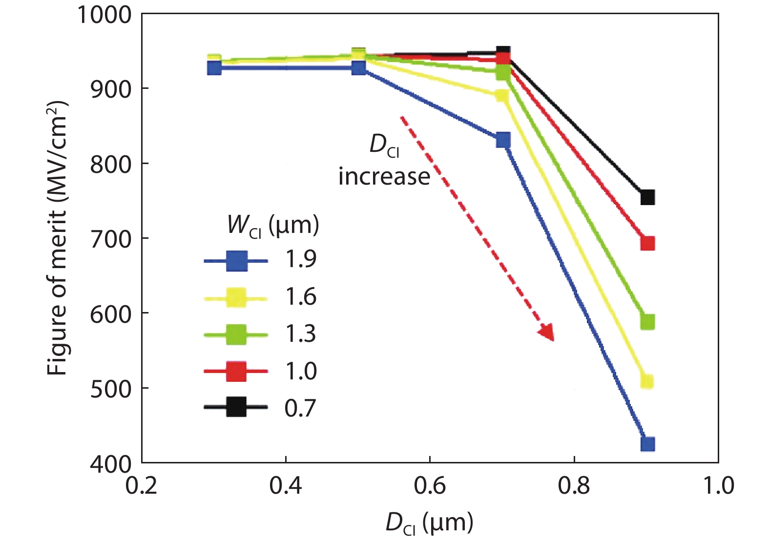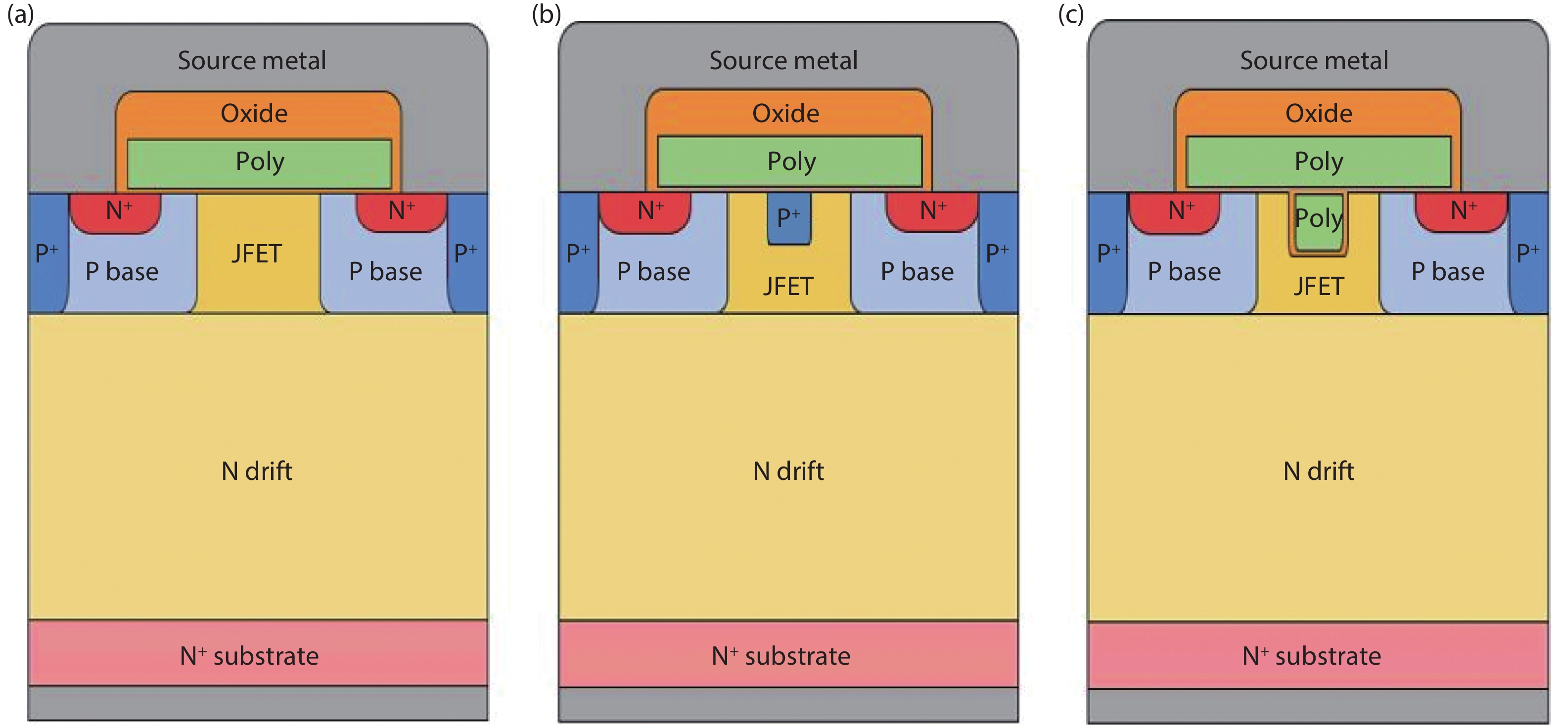
Fig. 1.
(Color online) Schematic cross-sectional structure of (a) C-MOSFET, (b) CI-MOSFET, and (c) DG-MOSFET.
ARTICLES
Corresponding author: Kwangsoo Kim, kimks@sogang.ac.kr
Abstract: In this paper, a 4H-SiC DMOSFET with a source-contacted dummy gate (DG-MOSFET) is proposed and analyzed through Sentaurus TCAD and PSIM simulations. The source-contacted MOS structure forms fewer depletion regions than the PN junction. Therefore, the overlapping region between the gate and the drain can be significantly reduced while limiting RON degradation. As a result, the DG-MOSFET offers an improved high-frequency figure of merit (HF-FOM) over the conventional DMOSFET (C-MOSFET) and central-implant MOSFET (CI-MOSFET). The HF-FOM (RON×QGD) of the DG-MOSFET was improved by 59.2% and 22.2% compared with those of the C-MOSFET and CI-MOSFET, respectively. In a double-pulse test, the DG-MOSFET could save total power losses of 53.4% and 5.51%, respectively. Moreover, in a power circuit simulation, the switching power loss was reduced by 61.9% and 12.7% in a buck converter and 61% and 9.6% in a boost converter.
Key words: 4H-SiC, MOSFET, dummy-gate, gate-drain charge, switching loss
| [1] |
Zhang M, Wei J, Jiang H P, et al. A new SiC trench MOSFET structure with protruded p-base for low oxide field and enhanced switching performance. IEEE Trans Device Mater Relib, 2017, 17, 432 doi: 10.1109/TDMR.2017.2694220
|
| [2] |
Cooper J A, Agarwal A. SiC power-switching devices-the second electronics revolution. Proc IEEE, 2002, 90, 956 doi: 10.1109/JPROC.2002.1021561
|
| [3] |
Du Y, Baek S, Bhattacharya S, et al. High-voltage high-frequency transformer design for a 7.2 kV to 120 V/240 V 20 kVA solid state transformer. IECON 2010 – 36th Annual Conference on IEEE Industrial Electronics Society, 2010, 493
|
| [4] |
Ozdemir S, Acar F, Selamoigullari U. Comparison of silicon carbide MOSFET and IGBT based electric vehicle traction inverters. 2015 International Conference on Electrical Engineering and Informatics (ICEEI), 2015, 1
|
| [5] |
Yano H, Nakao H, Hatayama T, et al. Increased channel mobility in 4H-SiC UMOSFETs using on-axis substrates. Mater Sci Forum, 2007, 556/557, 807 doi: 10.4028/www.scientific.net/MSF.556-557.807
|
| [6] |
Banzhaf C T, Grieb M, Trautmann A, et al. Characterization of diverse gate oxides on 4H-SiC 3D trench-MOS structures. Mater Sci Forum, 2013, 740–742, 691 doi: 10.4028/www.scientific.net/MSF.740-742.691
|
| [7] |
Agarwal A K, Siergiej R R, Seshadri S, et al. A critical look at the performance advantages and limitations of 4H-SiC power UMOSFET structures. 8th International Symposium on Power Semiconductor Devices and ICs (ISPSD), 1997, 70(20), 2732
|
| [8] |
T. C. A. C Synopsys Sentaurus Device Manual Synopsys, Inc., (Version O-2018.06). Mountail View, CA, USA
|
| [9] |
Zhang Q C J, Duc J, Hull B, et al. CIMOSFET: A new MOSFET on SiC with a superior Ron·Qgd figure of merit. Mater Sci Forum, 2015, 821–823, 765 doi: 10.4028/www.scientific.net/MSF.821-823.765
|
| [10] |
Jiang J Y, Wu T L, Zhao F, et al. Numerical study of 4H-SiC UMOSFETs with split-gate and P+ shielding. Energies, 2020, 13, 1122 doi: 10.3390/en13051122
|
| [11] |
Lombardi C, Manzini S, Saporito A, et al. A physically based mobility model for numerical simulation of nonplanar devices. IEEE Trans Comput-Aided Des Integr Circuits Syst, 1988, 7, 1164 doi: 10.1109/43.9186
|
| [12] |
Hatakeyama T, Nishio T, Ota C, et al. Physical modeling and scaling properties of 4H-SiC power devices. International Congerence on Simulation of Semiconductor Processed and Devices, 2005, 171
|
| [13] |
Zhao Y, Niwa H, Kimoto T. Impact ionization coefficients of 4H-SiC in a wide temperature range. Jpn J Appl Phys, 2019, 58, 018001 doi: 10.7567/1347-4065/aae985
|
| [14] |
Vudumula P, Kotamraju S. Design and optimization of 1.2-kV SiC planar inversion MOSFET using split dummy gate concept for high-frequency applications. IEEE Trans Electron Devices, 2019, 66, 5266 doi: 10.1109/TED.2019.2949459
|
| [15] |
Jiang J Y, Huang C F, Wu T L, et al. Simulation study of 4h-SiC trench MOSFETs with various gate structures. Electron Devices Technology and Manufacturing Conference (EDTM), 2019, 401
|
| [16] |
Sui Y, Tsuji T, Cooper J A. On-state characteristics of SiC power UMOSFETs on 115-μm drift layers. IEEE Electron Device Lett, 2005, 26, 255 doi: 10.1109/LED.2005.845495
|
| [17] |
Šimonka V, Hössinger A, Weinbub J, et al. Growth rates of dry thermal oxidation of 4H-silicon carbide. J Appl Phys, 2016, 120, 135705 doi: 10.1063/1.4964688
|
| [18] |
Singh R, Hefner A R. Reliability of SiC MOS devices. Solid-State Electron, 2004, 48, 1717 doi: 10.1016/j.sse.2004.05.005
|
| [19] |
Han K, Baliga B J, Sung W. A novel 1.2 kV 4H-SiC buffered-gate (BG) MOSFET: Analysis and experimental results. IEEE Electron Device Lett, 2018, 39, 248 doi: 10.1109/LED.2017.2785771
|
| [20] |
Baliga B J. Fundamentals of power semiconductor devices. Boston, MA: Springer, 2008
|
| [21] |
Wei J, Zhang M, Jiang H P, et al. Dynamic degradation in SiC trench MOSFET with a floating p-shield revealed with numerical simulations. IEEE Trans Electron Devices, 2017, 64, 2592 doi: 10.1109/TED.2017.2697763
|
| [22] |
Mohan N, Undeland T M, Robbins W P. Power electronics: Converters, applications, and design. John Wiley & Sons, 2003
|
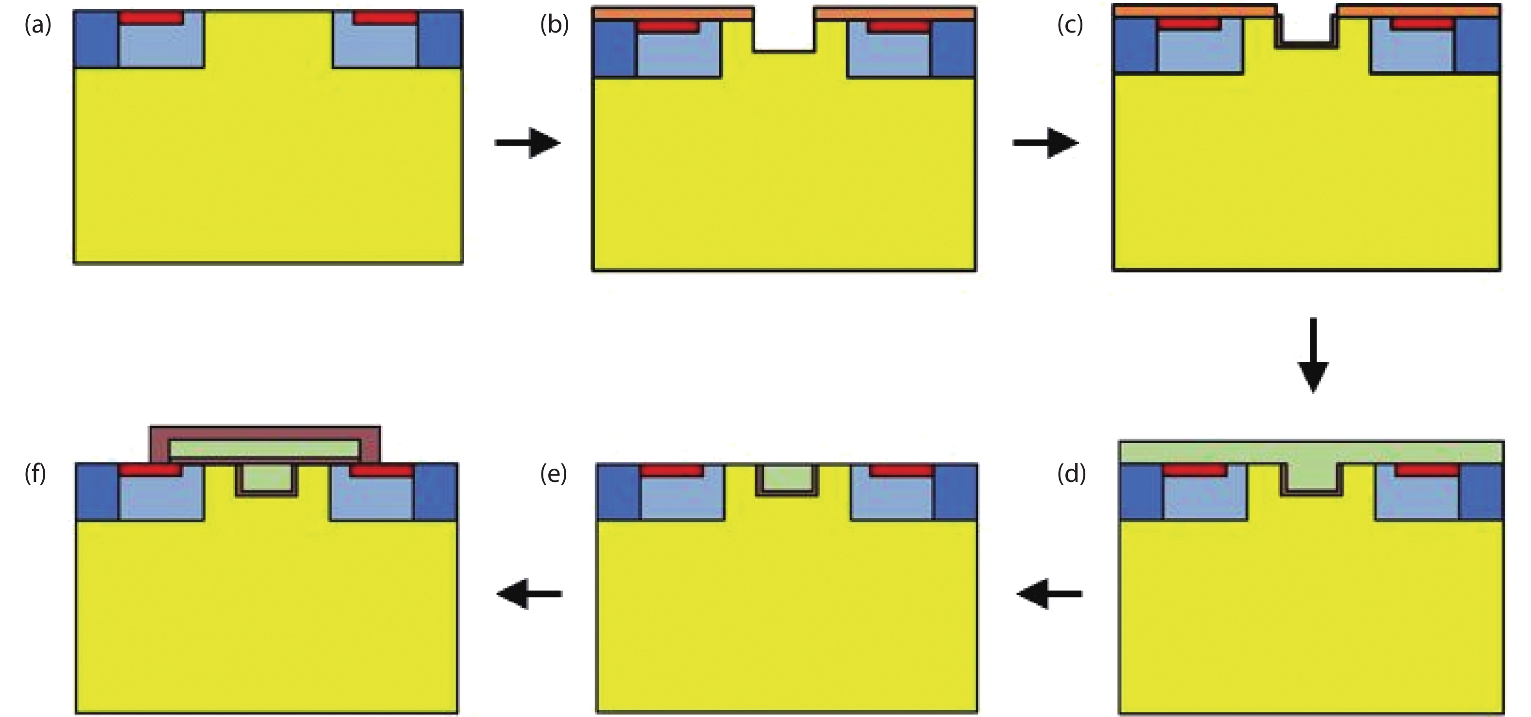

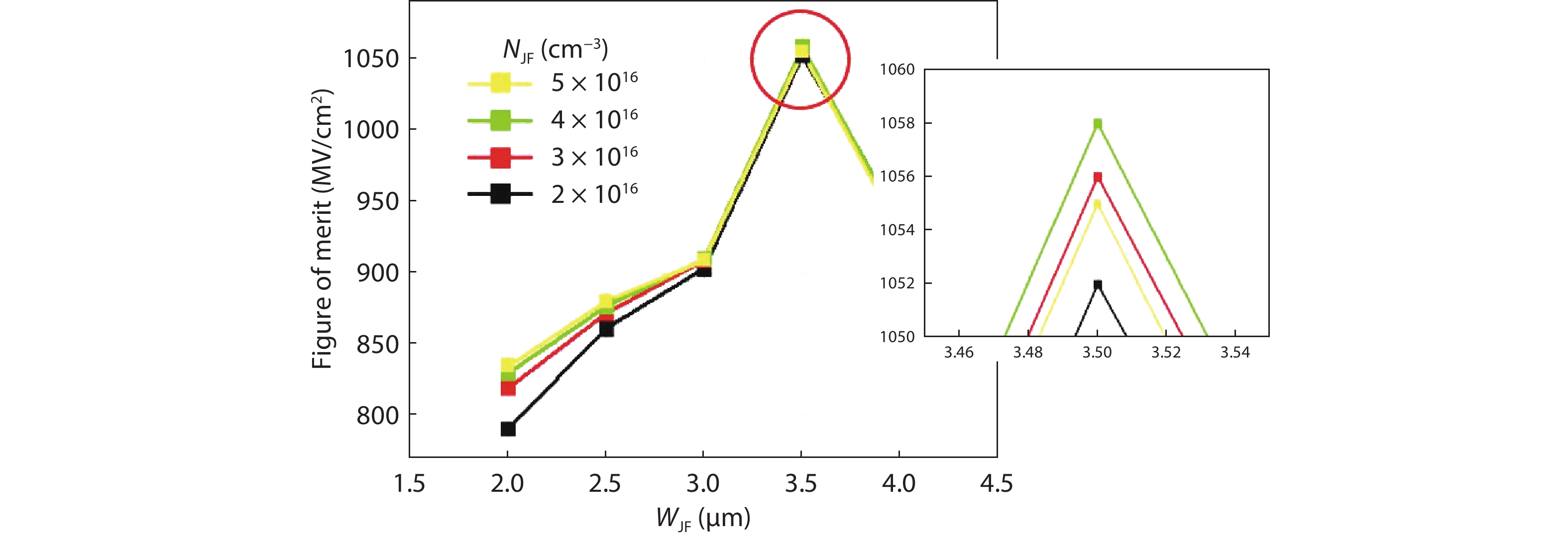
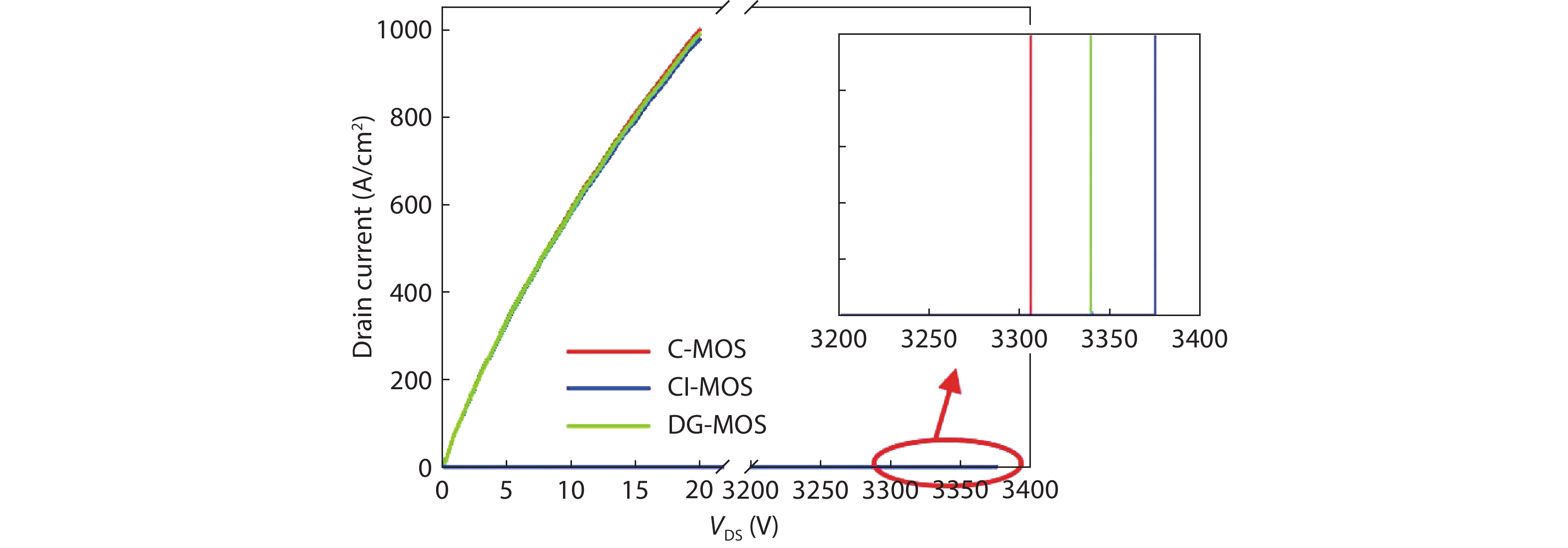
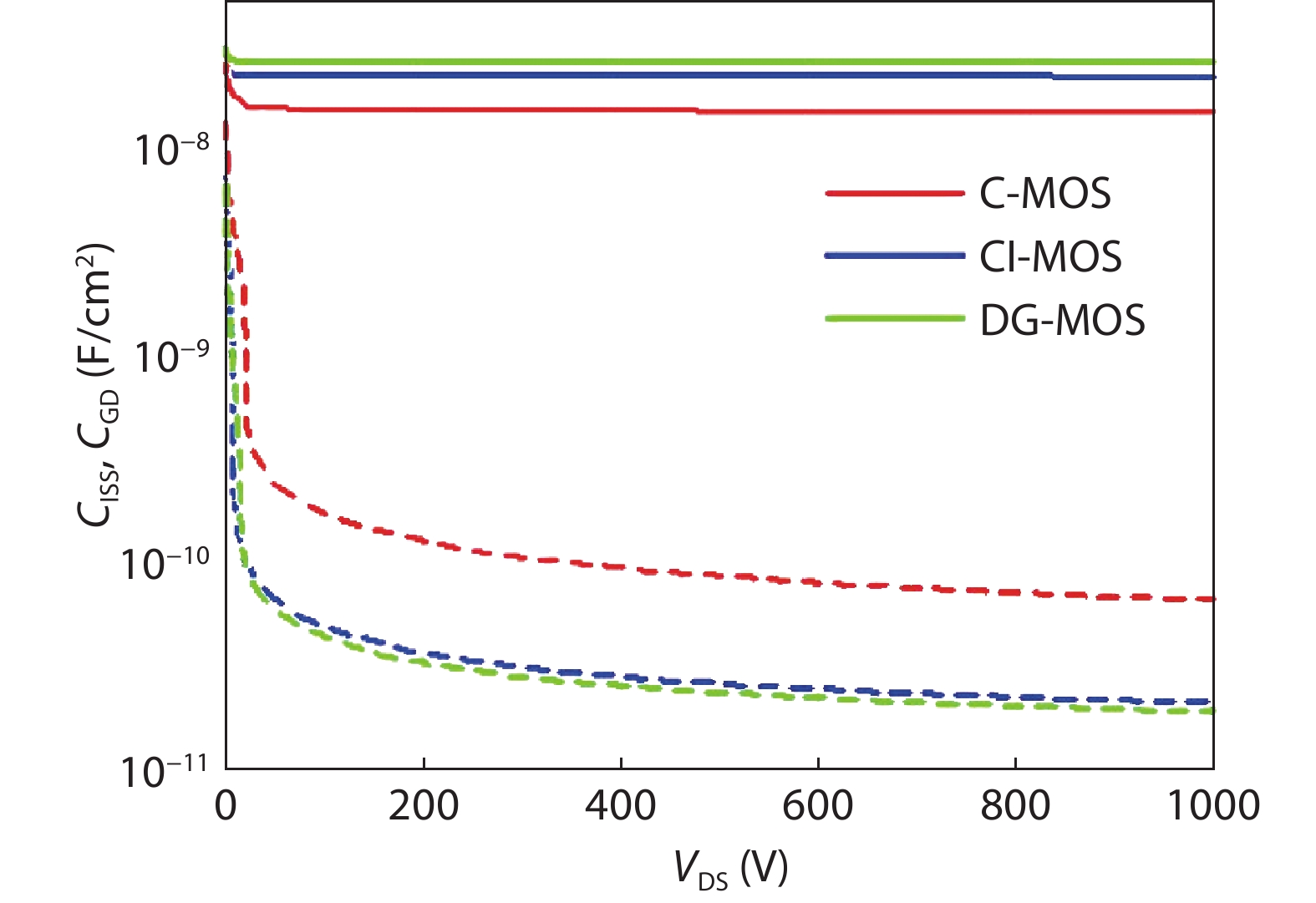
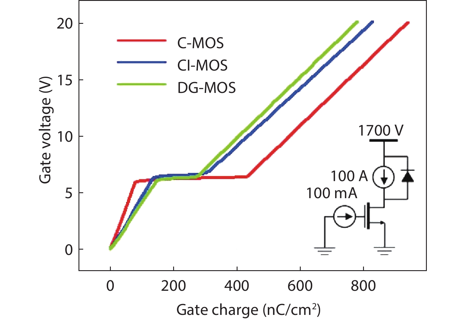
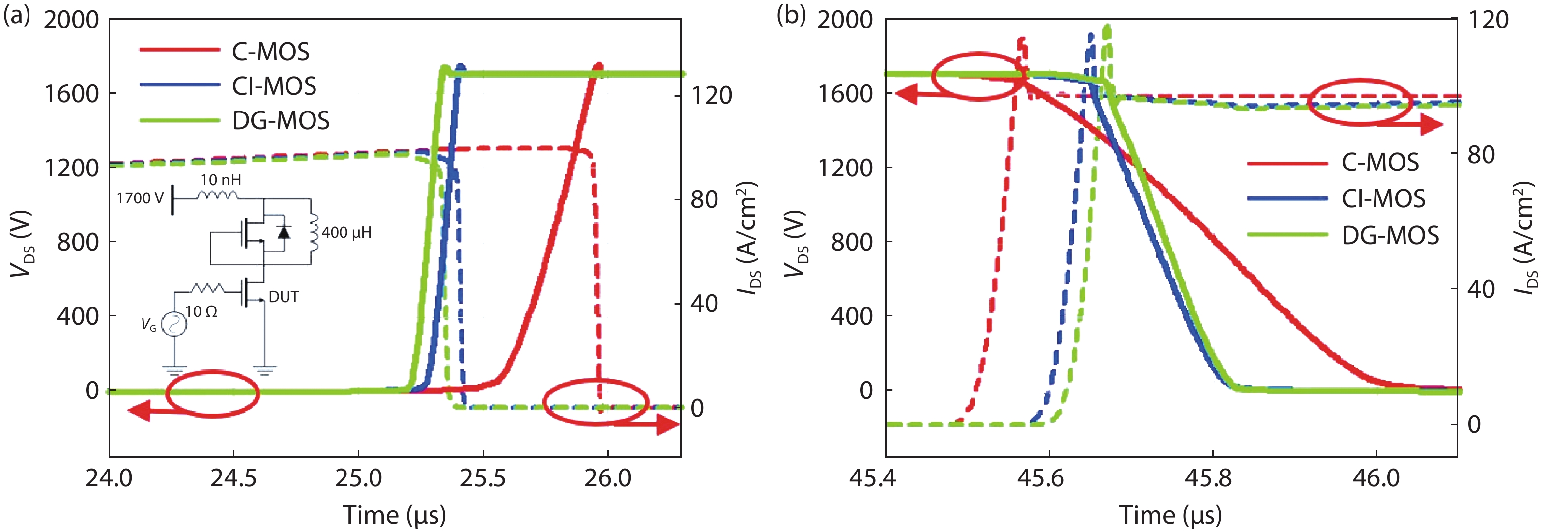
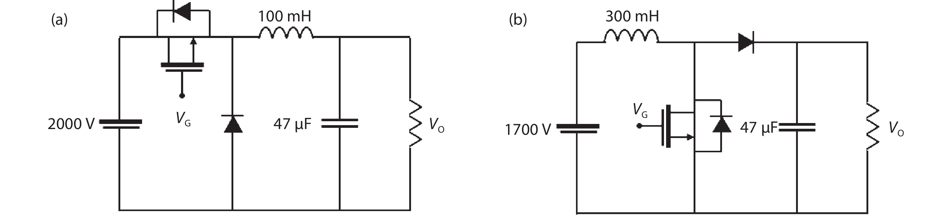

Table 1. Static characteristics of the optimized three structures.
| Parameter | C-MOSFET | CI-MOSFET | DG-MOSFET |
| RON (mΩ∙cm2) | 10.34 | 12.01 | 11.91 |
| BV (V) | 3305 | 3374 | 3343 |
| FOM (MW/cm2) | 1056 | 947 | 934 |
 DownLoad: CSV
Table 2. Capacitance and gate charge values of the three structures.
| Parameter | C-MOSFET | CI-MOSFET | DG-MOSFET |
| CISS (nF/cm2) | 14.8 | 21.9 | 25.7 |
| CGD (pF/cm2) | 66.67 | 21.12 | 19.36 |
| QGD (nC/cm2) | 353.1 | 159.5 | 125.3 |
| RON×QGD (mΩ∙nC) | 3651 | 1916 | 1492 |
| CRSS and CGD were simulated at VDS = 1000 V and QGD was simulated at IGS = 100 mA and VDD = 1700 V. | |||
DownLoad: CSV
Table 3. Double-pulse test simulation results.
| Parameter | C-MOSFET | CI-MOSFET | DG-MOSFET |
| EON (mJ/cm2) | 41.9 | 17.27 | 16.03 |
| EOFF (mJ/cm2) | 11.27 | 7.84 | 7.68 |
| ESW (mJ/cm2) | 53.17 | 25.11 | 23.71 |
DownLoad: CSV
Table 4. Power simulation results (f = 500 kHz).
| Power circuit | C-MOSFET | CI-MOSFET | DG-MOSFET |
| Buck converter (kW) | 20.616 | 8.934 | 7.784 |
| Boost converter (kW) | 48.731 | 20.923 | 18.901 |
DownLoad: CSV
| [1] |
Zhang M, Wei J, Jiang H P, et al. A new SiC trench MOSFET structure with protruded p-base for low oxide field and enhanced switching performance. IEEE Trans Device Mater Relib, 2017, 17, 432 doi: 10.1109/TDMR.2017.2694220
|
| [2] |
Cooper J A, Agarwal A. SiC power-switching devices-the second electronics revolution. Proc IEEE, 2002, 90, 956 doi: 10.1109/JPROC.2002.1021561
|
| [3] |
Du Y, Baek S, Bhattacharya S, et al. High-voltage high-frequency transformer design for a 7.2 kV to 120 V/240 V 20 kVA solid state transformer. IECON 2010 – 36th Annual Conference on IEEE Industrial Electronics Society, 2010, 493
|
| [4] |
Ozdemir S, Acar F, Selamoigullari U. Comparison of silicon carbide MOSFET and IGBT based electric vehicle traction inverters. 2015 International Conference on Electrical Engineering and Informatics (ICEEI), 2015, 1
|
| [5] |
Yano H, Nakao H, Hatayama T, et al. Increased channel mobility in 4H-SiC UMOSFETs using on-axis substrates. Mater Sci Forum, 2007, 556/557, 807 doi: 10.4028/www.scientific.net/MSF.556-557.807
|
| [6] |
Banzhaf C T, Grieb M, Trautmann A, et al. Characterization of diverse gate oxides on 4H-SiC 3D trench-MOS structures. Mater Sci Forum, 2013, 740–742, 691 doi: 10.4028/www.scientific.net/MSF.740-742.691
|
| [7] |
Agarwal A K, Siergiej R R, Seshadri S, et al. A critical look at the performance advantages and limitations of 4H-SiC power UMOSFET structures. 8th International Symposium on Power Semiconductor Devices and ICs (ISPSD), 1997, 70(20), 2732
|
| [8] |
T. C. A. C Synopsys Sentaurus Device Manual Synopsys, Inc., (Version O-2018.06). Mountail View, CA, USA
|
| [9] |
Zhang Q C J, Duc J, Hull B, et al. CIMOSFET: A new MOSFET on SiC with a superior Ron·Qgd figure of merit. Mater Sci Forum, 2015, 821–823, 765 doi: 10.4028/www.scientific.net/MSF.821-823.765
|
| [10] |
Jiang J Y, Wu T L, Zhao F, et al. Numerical study of 4H-SiC UMOSFETs with split-gate and P+ shielding. Energies, 2020, 13, 1122 doi: 10.3390/en13051122
|
| [11] |
Lombardi C, Manzini S, Saporito A, et al. A physically based mobility model for numerical simulation of nonplanar devices. IEEE Trans Comput-Aided Des Integr Circuits Syst, 1988, 7, 1164 doi: 10.1109/43.9186
|
| [12] |
Hatakeyama T, Nishio T, Ota C, et al. Physical modeling and scaling properties of 4H-SiC power devices. International Congerence on Simulation of Semiconductor Processed and Devices, 2005, 171
|
| [13] |
Zhao Y, Niwa H, Kimoto T. Impact ionization coefficients of 4H-SiC in a wide temperature range. Jpn J Appl Phys, 2019, 58, 018001 doi: 10.7567/1347-4065/aae985
|
| [14] |
Vudumula P, Kotamraju S. Design and optimization of 1.2-kV SiC planar inversion MOSFET using split dummy gate concept for high-frequency applications. IEEE Trans Electron Devices, 2019, 66, 5266 doi: 10.1109/TED.2019.2949459
|
| [15] |
Jiang J Y, Huang C F, Wu T L, et al. Simulation study of 4h-SiC trench MOSFETs with various gate structures. Electron Devices Technology and Manufacturing Conference (EDTM), 2019, 401
|
| [16] |
Sui Y, Tsuji T, Cooper J A. On-state characteristics of SiC power UMOSFETs on 115-μm drift layers. IEEE Electron Device Lett, 2005, 26, 255 doi: 10.1109/LED.2005.845495
|
| [17] |
Šimonka V, Hössinger A, Weinbub J, et al. Growth rates of dry thermal oxidation of 4H-silicon carbide. J Appl Phys, 2016, 120, 135705 doi: 10.1063/1.4964688
|
| [18] |
Singh R, Hefner A R. Reliability of SiC MOS devices. Solid-State Electron, 2004, 48, 1717 doi: 10.1016/j.sse.2004.05.005
|
| [19] |
Han K, Baliga B J, Sung W. A novel 1.2 kV 4H-SiC buffered-gate (BG) MOSFET: Analysis and experimental results. IEEE Electron Device Lett, 2018, 39, 248 doi: 10.1109/LED.2017.2785771
|
| [20] |
Baliga B J. Fundamentals of power semiconductor devices. Boston, MA: Springer, 2008
|
| [21] |
Wei J, Zhang M, Jiang H P, et al. Dynamic degradation in SiC trench MOSFET with a floating p-shield revealed with numerical simulations. IEEE Trans Electron Devices, 2017, 64, 2592 doi: 10.1109/TED.2017.2697763
|
| [22] |
Mohan N, Undeland T M, Robbins W P. Power electronics: Converters, applications, and design. John Wiley & Sons, 2003
|


Article views: 3470 Times PDF downloads: 173 Times Cited by: 0 Times
Received: 08 October 2010 Revised: 06 November 2020 Online: Accepted Manuscript: 02 December 2020Uncorrected proof: 18 December 2020Published: 01 June 2021
| Citation: |
Kyuhyun Cha, Kwangsoo Kim. 3.3 kV 4H-SiC DMOSFET with a source-contacted dummy gate for high-frequency applications[J]. Journal of Semiconductors, 2021, 42(6): 062801. doi: 10.1088/1674-4926/42/6/062801
K Cha, K Kim, 3.3 kV 4H-SiC DMOSFET with a source-contacted dummy gate for high-frequency applications[J]. J. Semicond., 2021, 42(6): 062801. doi: 10.1088/1674-4926/42/6/062801.
Export: BibTex EndNote

|
| [1] |
Zhang M, Wei J, Jiang H P, et al. A new SiC trench MOSFET structure with protruded p-base for low oxide field and enhanced switching performance. IEEE Trans Device Mater Relib, 2017, 17, 432 doi: 10.1109/TDMR.2017.2694220
|
| [2] |
Cooper J A, Agarwal A. SiC power-switching devices-the second electronics revolution. Proc IEEE, 2002, 90, 956 doi: 10.1109/JPROC.2002.1021561
|
| [3] |
Du Y, Baek S, Bhattacharya S, et al. High-voltage high-frequency transformer design for a 7.2 kV to 120 V/240 V 20 kVA solid state transformer. IECON 2010 – 36th Annual Conference on IEEE Industrial Electronics Society, 2010, 493
|
| [4] |
Ozdemir S, Acar F, Selamoigullari U. Comparison of silicon carbide MOSFET and IGBT based electric vehicle traction inverters. 2015 International Conference on Electrical Engineering and Informatics (ICEEI), 2015, 1
|
| [5] |
Yano H, Nakao H, Hatayama T, et al. Increased channel mobility in 4H-SiC UMOSFETs using on-axis substrates. Mater Sci Forum, 2007, 556/557, 807 doi: 10.4028/www.scientific.net/MSF.556-557.807
|
| [6] |
Banzhaf C T, Grieb M, Trautmann A, et al. Characterization of diverse gate oxides on 4H-SiC 3D trench-MOS structures. Mater Sci Forum, 2013, 740–742, 691 doi: 10.4028/www.scientific.net/MSF.740-742.691
|
| [7] |
Agarwal A K, Siergiej R R, Seshadri S, et al. A critical look at the performance advantages and limitations of 4H-SiC power UMOSFET structures. 8th International Symposium on Power Semiconductor Devices and ICs (ISPSD), 1997, 70(20), 2732
|
| [8] |
T. C. A. C Synopsys Sentaurus Device Manual Synopsys, Inc., (Version O-2018.06). Mountail View, CA, USA
|
| [9] |
Zhang Q C J, Duc J, Hull B, et al. CIMOSFET: A new MOSFET on SiC with a superior Ron·Qgd figure of merit. Mater Sci Forum, 2015, 821–823, 765 doi: 10.4028/www.scientific.net/MSF.821-823.765
|
| [10] |
Jiang J Y, Wu T L, Zhao F, et al. Numerical study of 4H-SiC UMOSFETs with split-gate and P+ shielding. Energies, 2020, 13, 1122 doi: 10.3390/en13051122
|
| [11] |
Lombardi C, Manzini S, Saporito A, et al. A physically based mobility model for numerical simulation of nonplanar devices. IEEE Trans Comput-Aided Des Integr Circuits Syst, 1988, 7, 1164 doi: 10.1109/43.9186
|
| [12] |
Hatakeyama T, Nishio T, Ota C, et al. Physical modeling and scaling properties of 4H-SiC power devices. International Congerence on Simulation of Semiconductor Processed and Devices, 2005, 171
|
| [13] |
Zhao Y, Niwa H, Kimoto T. Impact ionization coefficients of 4H-SiC in a wide temperature range. Jpn J Appl Phys, 2019, 58, 018001 doi: 10.7567/1347-4065/aae985
|
| [14] |
Vudumula P, Kotamraju S. Design and optimization of 1.2-kV SiC planar inversion MOSFET using split dummy gate concept for high-frequency applications. IEEE Trans Electron Devices, 2019, 66, 5266 doi: 10.1109/TED.2019.2949459
|
| [15] |
Jiang J Y, Huang C F, Wu T L, et al. Simulation study of 4h-SiC trench MOSFETs with various gate structures. Electron Devices Technology and Manufacturing Conference (EDTM), 2019, 401
|
| [16] |
Sui Y, Tsuji T, Cooper J A. On-state characteristics of SiC power UMOSFETs on 115-μm drift layers. IEEE Electron Device Lett, 2005, 26, 255 doi: 10.1109/LED.2005.845495
|
| [17] |
Šimonka V, Hössinger A, Weinbub J, et al. Growth rates of dry thermal oxidation of 4H-silicon carbide. J Appl Phys, 2016, 120, 135705 doi: 10.1063/1.4964688
|
| [18] |
Singh R, Hefner A R. Reliability of SiC MOS devices. Solid-State Electron, 2004, 48, 1717 doi: 10.1016/j.sse.2004.05.005
|
| [19] |
Han K, Baliga B J, Sung W. A novel 1.2 kV 4H-SiC buffered-gate (BG) MOSFET: Analysis and experimental results. IEEE Electron Device Lett, 2018, 39, 248 doi: 10.1109/LED.2017.2785771
|
| [20] |
Baliga B J. Fundamentals of power semiconductor devices. Boston, MA: Springer, 2008
|
| [21] |
Wei J, Zhang M, Jiang H P, et al. Dynamic degradation in SiC trench MOSFET with a floating p-shield revealed with numerical simulations. IEEE Trans Electron Devices, 2017, 64, 2592 doi: 10.1109/TED.2017.2697763
|
| [22] |
Mohan N, Undeland T M, Robbins W P. Power electronics: Converters, applications, and design. John Wiley & Sons, 2003
|

 WeChat ID
Journal of Semiconductors © 2017 All Rights Reserved 京ICP备05085259号-2