


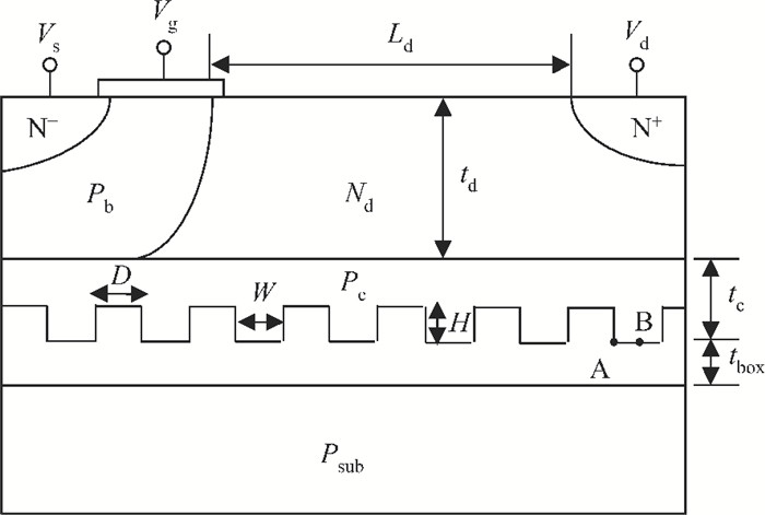
Fig. 1.
Schematic cross section of CL T-LDMOS.
SEMICONDUCTOR DEVICES
Qiuming Zhao1, Qi Li1, , Ning Tang1 and Yongchang Li2
Corresponding author: Li Qi, Email:lqmoon@gmail.com
Abstract: A new silicon-on-insulator (SOI) high-voltage MOSFET structure with a compensation layer on the trenched buried oxide layer (CL T-LDMOS) is proposed. The high density inverse interface charges at the top surface of the buried oxide layer (BOX) enhance the electric field in the BOX and a uniform surface electric field profile is obtained, which results in the enhancement of the breakdown voltage (BV). The compensation layer can provide additional P-type charges, and the optimal drift region concentration is increased in order to satisfy the reduced surface electric field (RESURF) condition. The numerical simulation results indicate that the vertical electric field in the BOX increases to 6 MV/cm and the BV of the proposed device increases by 300% in comparison to a conventional SOI LDMOS, while maintaining low on-resistance.
Key words: trenched buried oxide layer, breakdown voltage, on-resistance, compensation layer
| [1] |
Merchant S, Arnold E, Baumgart S, et al. Realization of high breakdown voltage (> 700 V) in thin SOI device. ISPSD, 1991:31
|
| [2] |
Li Q, Zhang B, Li Z. A new partial SOI high voltage device with double-faced step buried oxide structure. Acta Physica Sinica, 2008, 57(10):6565 http://wulixb.iphy.ac.cn/EN/Y2008/V57/I10/6565
|
| [3] |
Ramakrishna T, Shyam H, Sankara E M. Realizing high breakdown voltage (> 600 V) in partial SOI technology. Solid-State Electron, 2004, 48:1655 doi: 10.1016/j.sse.2004.04.005
|
| [4] |
Luo X R, Li Z J, Zhang B, et al. A novel structure and its breakdown mechanism of a SOI high voltage device with a shield trench. Chinese Journal of Semiconductors, 2005, 26(11):2154 http://www.sciencedirect.com/science/article/pii/S138694771530196X
|
| [5] |
Zhang B, Li Z, Hu S, et al. Field enhancement for dielectric layer of high-voltage devices on silicon on insulator. IEEE Trans Electron Devices, 2009, 56(10):2327 doi: 10.1109/TED.2009.2028405
|
| [6] |
Wang W L, Zhang B, Chen W J, et al. High voltage SOI SJ-LDMOS with dynamic back-gate voltage. Electron Lett, 2009, 45(4):233 doi: 10.1049/el:20093005
|
| [7] |
Luo X, Zhang B, Li Z, et al. A novel 700-V SOI LDMOS with double-sided trench. IEEE Electron Device Lett, 2007, 28(5):422 doi: 10.1109/LED.2007.894648
|
| [8] |
Ge R, Luo X, Jiang Y H, et al. A low on-resistance SOI LDMOS using a trench gate and a recessed drain. Journal of Semiconductors, 2012, 33(7):074005 doi: 10.1088/1674-4926/33/7/074005
|
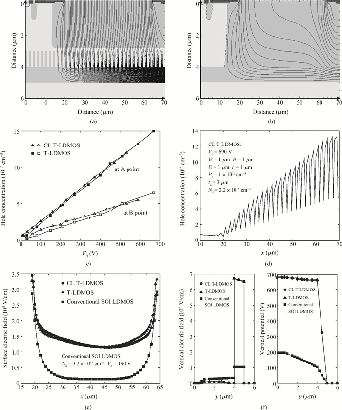
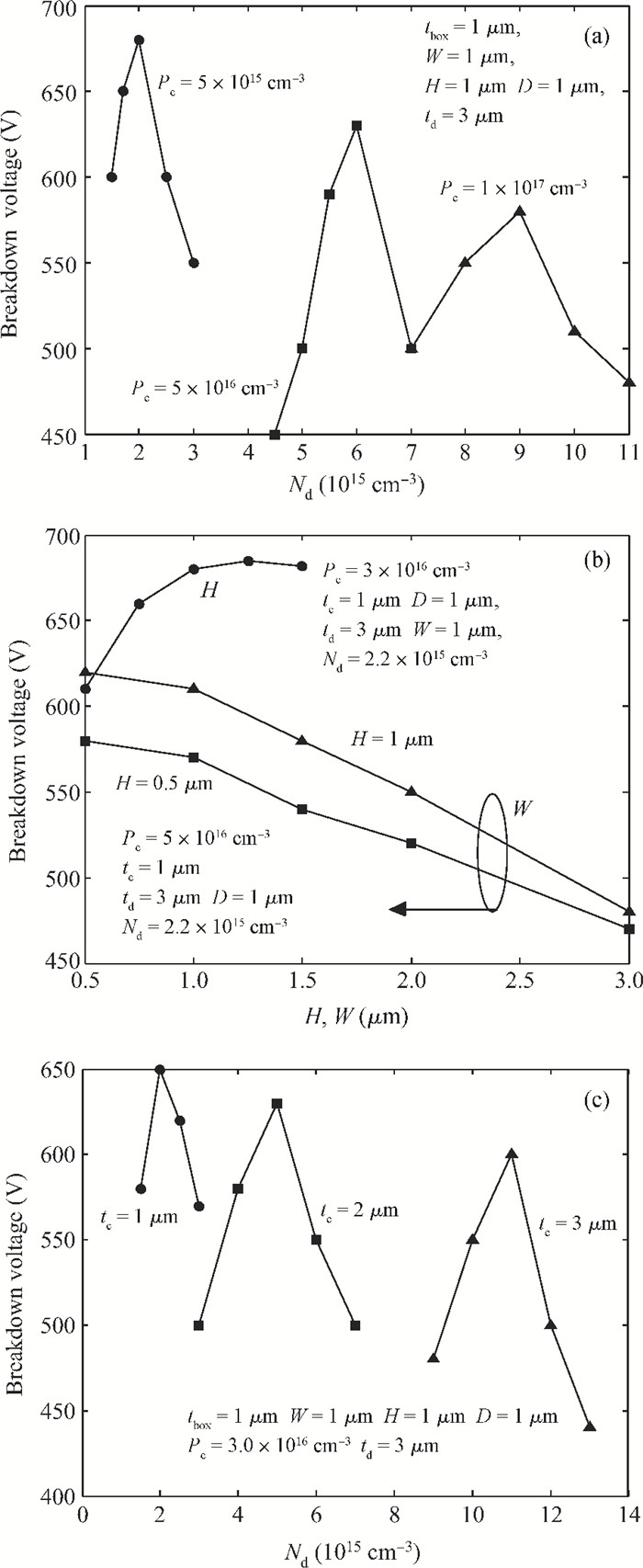
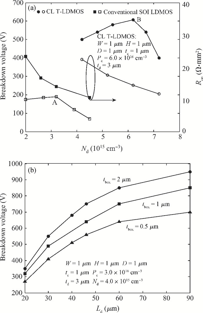
Table 1. Comparison performances between the CL T-LDMOS and the other SOI LDMOS with a trenched BOX.

|
| [1] |
Merchant S, Arnold E, Baumgart S, et al. Realization of high breakdown voltage (> 700 V) in thin SOI device. ISPSD, 1991:31
|
| [2] |
Li Q, Zhang B, Li Z. A new partial SOI high voltage device with double-faced step buried oxide structure. Acta Physica Sinica, 2008, 57(10):6565 http://wulixb.iphy.ac.cn/EN/Y2008/V57/I10/6565
|
| [3] |
Ramakrishna T, Shyam H, Sankara E M. Realizing high breakdown voltage (> 600 V) in partial SOI technology. Solid-State Electron, 2004, 48:1655 doi: 10.1016/j.sse.2004.04.005
|
| [4] |
Luo X R, Li Z J, Zhang B, et al. A novel structure and its breakdown mechanism of a SOI high voltage device with a shield trench. Chinese Journal of Semiconductors, 2005, 26(11):2154 http://www.sciencedirect.com/science/article/pii/S138694771530196X
|
| [5] |
Zhang B, Li Z, Hu S, et al. Field enhancement for dielectric layer of high-voltage devices on silicon on insulator. IEEE Trans Electron Devices, 2009, 56(10):2327 doi: 10.1109/TED.2009.2028405
|
| [6] |
Wang W L, Zhang B, Chen W J, et al. High voltage SOI SJ-LDMOS with dynamic back-gate voltage. Electron Lett, 2009, 45(4):233 doi: 10.1049/el:20093005
|
| [7] |
Luo X, Zhang B, Li Z, et al. A novel 700-V SOI LDMOS with double-sided trench. IEEE Electron Device Lett, 2007, 28(5):422 doi: 10.1109/LED.2007.894648
|
| [8] |
Ge R, Luo X, Jiang Y H, et al. A low on-resistance SOI LDMOS using a trench gate and a recessed drain. Journal of Semiconductors, 2012, 33(7):074005 doi: 10.1088/1674-4926/33/7/074005
|


Article views: 3173 Times PDF downloads: 26 Times Cited by: 0 Times
Received: 02 July 2012 Revised: 26 September 2012 Online: Published: 01 March 2013
| Citation: |
Qiuming Zhao, Qi Li, Ning Tang, Yongchang Li. A high-voltage SOI MOSFET with a compensation layer on the trenched buried oxide layer[J]. Journal of Semiconductors, 2013, 34(3): 034003. doi: 10.1088/1674-4926/34/3/034003
****
Q M Zhao, Q Li, N Tang, Y C Li. A high-voltage SOI MOSFET with a compensation layer on the trenched buried oxide layer[J]. J. Semicond., 2013, 34(3): 034003. doi: 10.1088/1674-4926/34/3/034003.

|
| [1] |
Merchant S, Arnold E, Baumgart S, et al. Realization of high breakdown voltage (> 700 V) in thin SOI device. ISPSD, 1991:31
|
| [2] |
Li Q, Zhang B, Li Z. A new partial SOI high voltage device with double-faced step buried oxide structure. Acta Physica Sinica, 2008, 57(10):6565 http://wulixb.iphy.ac.cn/EN/Y2008/V57/I10/6565
|
| [3] |
Ramakrishna T, Shyam H, Sankara E M. Realizing high breakdown voltage (> 600 V) in partial SOI technology. Solid-State Electron, 2004, 48:1655 doi: 10.1016/j.sse.2004.04.005
|
| [4] |
Luo X R, Li Z J, Zhang B, et al. A novel structure and its breakdown mechanism of a SOI high voltage device with a shield trench. Chinese Journal of Semiconductors, 2005, 26(11):2154 http://www.sciencedirect.com/science/article/pii/S138694771530196X
|
| [5] |
Zhang B, Li Z, Hu S, et al. Field enhancement for dielectric layer of high-voltage devices on silicon on insulator. IEEE Trans Electron Devices, 2009, 56(10):2327 doi: 10.1109/TED.2009.2028405
|
| [6] |
Wang W L, Zhang B, Chen W J, et al. High voltage SOI SJ-LDMOS with dynamic back-gate voltage. Electron Lett, 2009, 45(4):233 doi: 10.1049/el:20093005
|
| [7] |
Luo X, Zhang B, Li Z, et al. A novel 700-V SOI LDMOS with double-sided trench. IEEE Electron Device Lett, 2007, 28(5):422 doi: 10.1109/LED.2007.894648
|
| [8] |
Ge R, Luo X, Jiang Y H, et al. A low on-resistance SOI LDMOS using a trench gate and a recessed drain. Journal of Semiconductors, 2012, 33(7):074005 doi: 10.1088/1674-4926/33/7/074005
|

 WeChat ID
Journal of Semiconductors © 2017 All Rights Reserved 京ICP备05085259号-2

 DownLoad:

