| Citation: |
Meile Wu, Xiaoshi Jin, Rongyan Chuai, Xi Liu, Jong-Ho Lee. Simulation study on short channel double-gate junctionless field-effect transistors[J]. Journal of Semiconductors, 2013, 34(3): 034004. doi: 10.1088/1674-4926/34/3/034004
****
M L Wu, X S Jin, R Y Chuai, X Liu, J H Lee. Simulation study on short channel double-gate junctionless field-effect transistors[J]. J. Semicond., 2013, 34(3): 034004. doi: 10.1088/1674-4926/34/3/034004.
|
Simulation study on short channel double-gate junctionless field-effect transistors
DOI: 10.1088/1674-4926/34/3/034004
More Information
-
Abstract
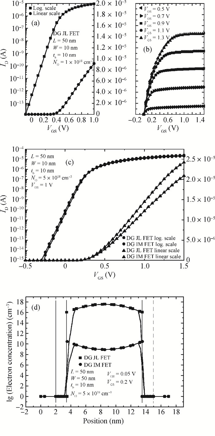
We study the characteristics of short channel double-gate (DG) junctionless (JL) FETs by device simulation. Output Ⅰ-Ⅴ characteristic degradations such as an extremely reduced channel length induced subthreshold slope increase and the threshold voltage shift due to variations of body doping and channel length have been systematically analyzed. Distributions of electron concentration, electric field and potential in the body channel region are also analyzed. Comparisons with conventional inversion-mode (IM) FETs, which can demonstrate the advantages of JL FETs, have also been performed. -
References
[1] Duarte J P, Kim M S, Choi S J, et al. A compact model of quantum electron density at the subthreshold region for double-gate junctionless transistor. IEEE Trans Electron Devices, 2012, 59(4):1008 doi: 10.1109/TED.2012.2185827[2] Jin X, Liu X, Lee J, et al. A continuous current model of fully-depleted symmetric double-gate MOSFETs considering a wide range of body doping concentrations. Semicond Sci Technol, 2010, 25(5):055018 doi: 10.1088/0268-1242/25/5/055018[3] Diagne B, Prégaldiny F, Lallement C, et al. Explicit compact model for symmetric double-gate MOSFETs including solutions for small-geometry effects. Solid-State Electron, 2008, 52(1):99 doi: 10.1016/j.sse.2007.06.020[4] Colinge J P, Lee C W, Afzalian A, et al. Nanowire transistors without junctions. Nat Nanotechnology, 2010, 5(3):225 doi: 10.1038/nnano.2010.15[5] Gnani E, Gnudi A, Reggiani S, et al. Theory of the junctionless nanowire FET. IEEE Trans Electron Devices, 2011, 58(9):2903 doi: 10.1109/TED.2011.2159608[6] Gnani E, Gnudi A, Reggiani S, et al. Numerical investigation on the junctionless nanowire FET. Solid-State Electron, 2012, 71:13 doi: 10.1016/j.sse.2011.10.013[7] Colinge J P, Ferain I, Kranti A, et al. Junctionless nanowire transistor:complementary metal-oxide-semiconductor without junctions. Sci Adv Mater, 2011, 3(3):477 doi: 10.1166/sam.2011.1163[8] SILVACO International. ATLAS User's Manual, 2005[9] Shoji M, Horiguchi S. Electronic structures and phonon limited electron mobility of double-gate silicon-on insulator Si inversion layers. J Appl Phys, 1999, 85:2722 doi: 10.1063/1.369589 -
Proportional views


 DownLoad:


