


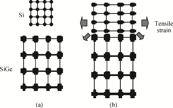
Fig. 1.
Schematic illustration of Si and SiGe atoms under biaxial strain.
SEMICONDUCTOR PHYSICS
EngSiew Kang1, , S Anwar2, M T Ahmadi1 and Razali Ismail1
Corresponding author: EngSiew Kang, Email:engsiew85@gmail.com
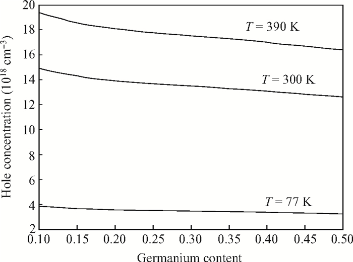
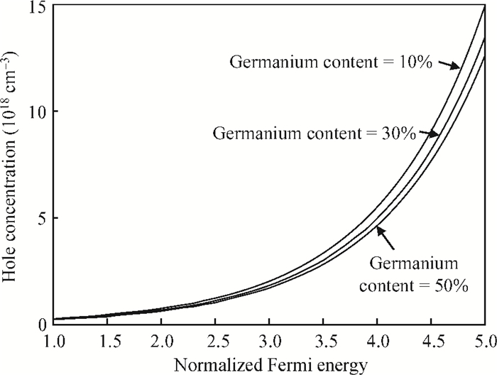
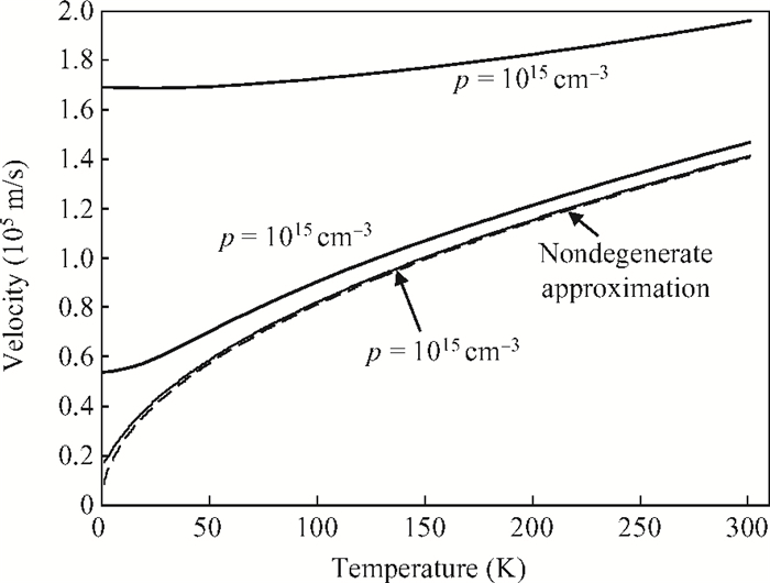
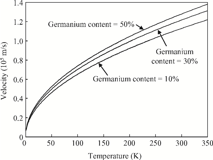
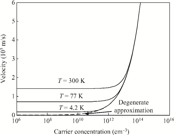
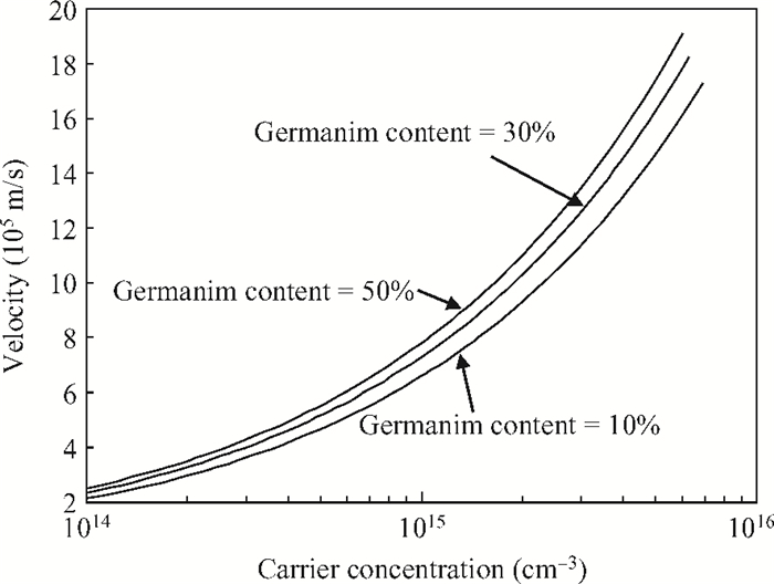
Abstract: The impact of the fraction of germanium on the carrier performance of two-dimensional strained silicon, which embraces both the non-degenerate and degenerate regimes, is developed. In this model, the Fermi integral of order zero is employed. The impact of the fraction of germanium on the relaxed Si1-xGex substrate (x), carrier concentration and temperature is reported. It is revealed that the effect of x on the hole concentration is dominant for a normalized Fermi energy of more than three, or in other words the non-degenerate regime. On the contrary, the x gradient has less influence in the degenerate regime. Furthermore, by increasing x there is an increase in the intrinsic velocity, particularly with high carrier concentration and temperature.
Keywords: germanium, intrinsic velocity, SiGe, hole concentration, two dimensional
| [1] |
Vogelsang T, Hofmann K R. Electron mobilities and high-field drift velocities in strained silicon on silicon-germanium substrate. Proc 50th Annu Device Res Conf Dig, 1992:34 http://ieeexplore.ieee.org/document/671857/keywords
|
| [2] |
Kumar M J, Venkataraman V, Nawal S. A simple analytical threshold voltage model of nanoscale single-layer fully depleted strained-silicon-on-insulator MOSFETs. IEEE Trans Electron Devices, 2006, 53(10):2500 doi: 10.1109/TED.2006.882041
|
| [3] |
Rim K, Anderson R, Boyd D, et al. Strained Si CMOS (SS CMOS) technology:opportunities and challenges. Solid-State Electron, 2003, 47:1133 doi: 10.1016/S0038-1101(03)00041-8
|
| [4] |
Rim K, Hoyt J L, Gibbons J F. Fabrication and analysis of deep submicron strained-Si n-MOSFET's. IEEE Trans Electron Devices, 2000, 47:1406 doi: 10.1109/16.848284
|
| [5] |
Saad I, Riyadi M A, Taghi M, et al. Analytical analysis of ballistic drift velocity in low-dimensional nano-devices. Fourth Asia International Conference on Mathematica/Analytical Modeling and Computer Simulation, Kota Kinabalu, Malaysia, 2010:601 http://ieeexplore.ieee.org/document/5489264/
|
| [6] |
Ahmadi M T, Lau H H, Ismail R, et al. Current-voltage characteristic of a silicon nanowire transistor. Microelectron J, 2009, 40:547 doi: 10.1016/j.mejo.2008.06.060
|
| [7] |
Arora V K. High-field distribution and mobility in semiconductors. Jpn J Appl Phys, 1985, 24:537 doi: 10.1143/JJAP.24.537
|
| [8] |
Lime F, Andrieu F, Derx J, et al. Low temperature characterization of effective mobility in uniaxially and biaxially strained nMOSFETs. Solid-State Electron, 2006, 50(4):644 doi: 10.1016/j.sse.2006.03.036
|
| [9] |
Tinoco J C, Garcia R, Iniguez B, et al. Threshold voltage model for bulk strained-silicon NMOSFETs. Semicond Sci Technol, 2008, 23(3):035017 doi: 10.1088/0268-1242/23/3/035017
|
| [10] |
Nayfeh H M, Hoyt J L, Antoniadis D A. A physically based analytical model for the threshold voltage of strained-Si n-MOSFETs. IEEE Trans Electron Devices, 2004, 51(12):2069 doi: 10.1109/TED.2004.838320
|
| [11] |
Briggs P J, Walker A B, Herbert D C. Modelling the influence of high currents on the cutoff frequency in Si/SiGe/Si heterojunction transistors. Semicond Sci Technol, 1998, 13:468 doi: 10.1088/0268-1242/13/5/005
|
| [12] |
Riyadi M A, Ahmadi M T, Susendo J E, et al. Physics-based simulation of carrier velocity in 2-dimensional P-type MOSFET. Third Asia International Conference on Modeling & Simulation, 2009:735 http://ieeexplore.ieee.org/document/5072079/keywords
|
| [13] |
Arora V K. Quantum engineering of nanoelectronic devices. Microelectron J, 2000, 31(11/12):853 http://ieeexplore.ieee.org/document/840526/?isnumber=18158&arnumber=840526&count=74&index=2
|
| [14] |
Ahmadi M T, Ismail R, Tan M L P, et al. The ultimate ballistic drift velocity in carbon nanotubes. J Nanomater, 2008, 2008:769250 https://pure.utm.my/en/publications/the-ultimate-ballistic-drift-velocity-in-carbon-nanotubes
|


Article views: 3136 Times PDF downloads: 81 Times Cited by: 0 Times
Received: 03 October 2012 Revised: 24 December 2012 Online: Published: 01 June 2013
| Citation: |
EngSiew Kang, S Anwar, M T Ahmadi, Razali Ismail. The impact of germanium in strained Si/relaxed Si1-xGex on carrier performance in non-degenerate and degenerate regimes[J]. Journal of Semiconductors, 2013, 34(6): 062001. doi: 10.1088/1674-4926/34/6/062001
****
E Kang, S Anwar, M T Ahmadi, R Ismail. The impact of germanium in strained Si/relaxed Si1-xGex on carrier performance in non-degenerate and degenerate regimes[J]. J. Semicond., 2013, 34(6): 062001. doi: 10.1088/1674-4926/34/6/062001.

|
| [1] |
Vogelsang T, Hofmann K R. Electron mobilities and high-field drift velocities in strained silicon on silicon-germanium substrate. Proc 50th Annu Device Res Conf Dig, 1992:34 http://ieeexplore.ieee.org/document/671857/keywords
|
| [2] |
Kumar M J, Venkataraman V, Nawal S. A simple analytical threshold voltage model of nanoscale single-layer fully depleted strained-silicon-on-insulator MOSFETs. IEEE Trans Electron Devices, 2006, 53(10):2500 doi: 10.1109/TED.2006.882041
|
| [3] |
Rim K, Anderson R, Boyd D, et al. Strained Si CMOS (SS CMOS) technology:opportunities and challenges. Solid-State Electron, 2003, 47:1133 doi: 10.1016/S0038-1101(03)00041-8
|
| [4] |
Rim K, Hoyt J L, Gibbons J F. Fabrication and analysis of deep submicron strained-Si n-MOSFET's. IEEE Trans Electron Devices, 2000, 47:1406 doi: 10.1109/16.848284
|
| [5] |
Saad I, Riyadi M A, Taghi M, et al. Analytical analysis of ballistic drift velocity in low-dimensional nano-devices. Fourth Asia International Conference on Mathematica/Analytical Modeling and Computer Simulation, Kota Kinabalu, Malaysia, 2010:601 http://ieeexplore.ieee.org/document/5489264/
|
| [6] |
Ahmadi M T, Lau H H, Ismail R, et al. Current-voltage characteristic of a silicon nanowire transistor. Microelectron J, 2009, 40:547 doi: 10.1016/j.mejo.2008.06.060
|
| [7] |
Arora V K. High-field distribution and mobility in semiconductors. Jpn J Appl Phys, 1985, 24:537 doi: 10.1143/JJAP.24.537
|
| [8] |
Lime F, Andrieu F, Derx J, et al. Low temperature characterization of effective mobility in uniaxially and biaxially strained nMOSFETs. Solid-State Electron, 2006, 50(4):644 doi: 10.1016/j.sse.2006.03.036
|
| [9] |
Tinoco J C, Garcia R, Iniguez B, et al. Threshold voltage model for bulk strained-silicon NMOSFETs. Semicond Sci Technol, 2008, 23(3):035017 doi: 10.1088/0268-1242/23/3/035017
|
| [10] |
Nayfeh H M, Hoyt J L, Antoniadis D A. A physically based analytical model for the threshold voltage of strained-Si n-MOSFETs. IEEE Trans Electron Devices, 2004, 51(12):2069 doi: 10.1109/TED.2004.838320
|
| [11] |
Briggs P J, Walker A B, Herbert D C. Modelling the influence of high currents on the cutoff frequency in Si/SiGe/Si heterojunction transistors. Semicond Sci Technol, 1998, 13:468 doi: 10.1088/0268-1242/13/5/005
|
| [12] |
Riyadi M A, Ahmadi M T, Susendo J E, et al. Physics-based simulation of carrier velocity in 2-dimensional P-type MOSFET. Third Asia International Conference on Modeling & Simulation, 2009:735 http://ieeexplore.ieee.org/document/5072079/keywords
|
| [13] |
Arora V K. Quantum engineering of nanoelectronic devices. Microelectron J, 2000, 31(11/12):853 http://ieeexplore.ieee.org/document/840526/?isnumber=18158&arnumber=840526&count=74&index=2
|
| [14] |
Ahmadi M T, Ismail R, Tan M L P, et al. The ultimate ballistic drift velocity in carbon nanotubes. J Nanomater, 2008, 2008:769250 https://pure.utm.my/en/publications/the-ultimate-ballistic-drift-velocity-in-carbon-nanotubes
|

 WeChat ID
Journal of Semiconductors © 2017 All Rights Reserved 京ICP备05085259号-2

 DownLoad:

