


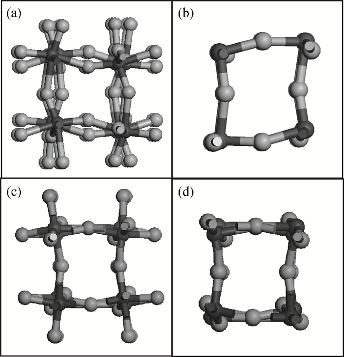
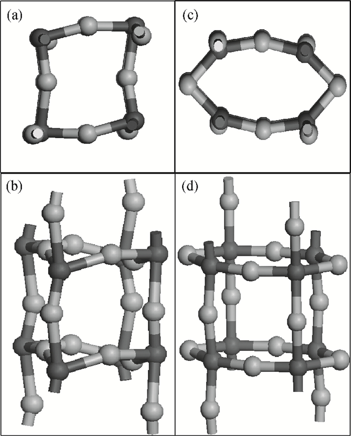
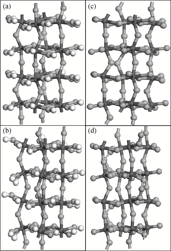
Fig. 1.
The top view of the [001]-(up) and [010]-oriented (bottom) WO$_3$ nanowire terminated by (a, c) oxygen monolayer, and (b, d) WO$_2$ plane. The dark and gray spheres represent W and O atoms, respectively.
SEMICONDUCTOR PHYSICS
Yuxiang Qin, Deyan Hua and Xiao Li
Corresponding author: Qin Yuxiang, Email:qinyuxiang@tju.edu.cn
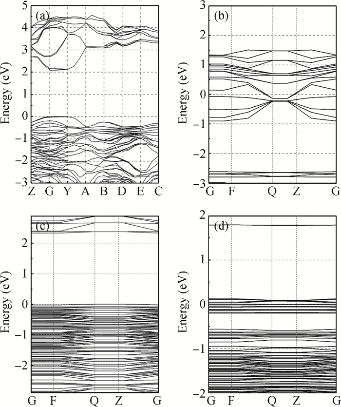
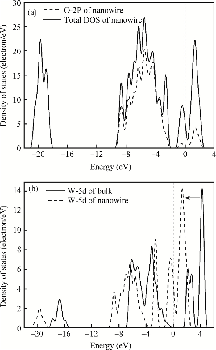
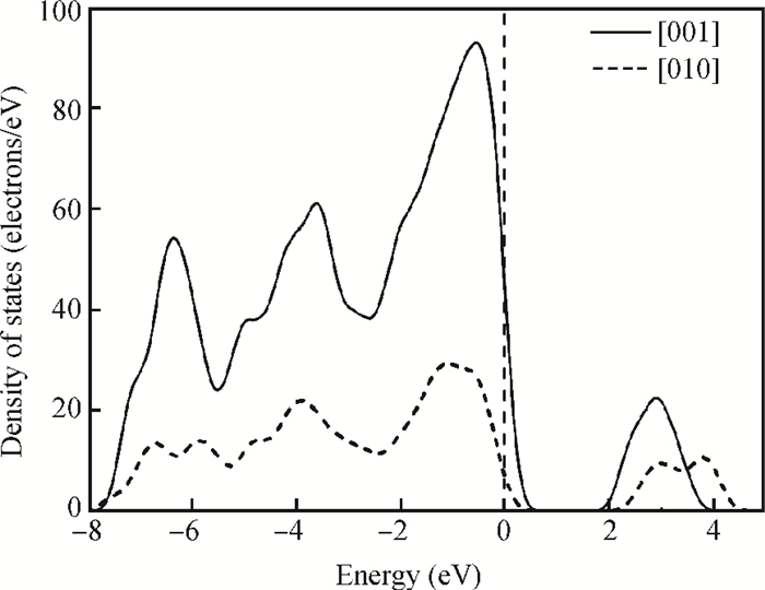
Abstract: The effects of the surface and orientation of a WO3 nanowire on the electronic structure are investigated by using first principles calculation based on density functional theory (DFT). The surface of the WO3 nanowire was terminated by a bare or hydrogenated oxygen monolayer or bare WO2 plane, and the[010]-and[001]-oriented nanowires with different sizes were introduced into the theoretical calculation to further study the dependence of electronic band structure on the wire size and orientation. The calculated results reveal that the surface structure, wire size and orientation have significant effects on the electronic band structure, bandgap, and density of states (DOS) of the WO3 nanowire. The optimized WO3 nanowire with different surface structures showed a markedly dissimilar band structure due to the different electronic states near the Fermi level, and the O-terminated[001] WO3 nanowire with hydrogenation can exhibit a reasonable indirect bandgap of 2.340 eV due to the quantum confinement effect, which is 0.257 eV wider than bulk WO3. Besides, the bandgap change is also related to the orientation-resulted surface reconstructed structure as well as wire size.
Key words: WO3 nanowire, density functional theory, electronic band structure, density of states
| [1] |
Gubbala S, Thangala J, Sunkara M K. Nanowire-based electrochromic devices. Sol Energy Mater Sol Cells, 2007, 91(9):813 doi: 10.1016/j.solmat.2007.01.016
|
| [2] |
Reyes L F, Hoel A. Gas sensor response of pure and activated WO3 nanoparticle films made by advanced reactive gas deposition. Sens Actuators B, 2006, 117(1):128 doi: 10.1016/j.snb.2005.11.008
|
| [3] |
Cao B, Chen J, Tang X, et al. Growth of monoclinic WO3 nanowire array for highly sensitive NO2 detection. J Mater Chem, 2009, 19:2323 doi: 10.1039/b816646c
|
| [4] |
Pan Z W, Dai Z R, Wang Z L. Nanobelts of semiconducting oxides. Science, 2001, 291:1947 doi: 10.1126/science.1058120
|
| [5] |
Baek Y, Yong K. Controlled growth and characterization of tungsten oxide nanowires using thermal evaporation of WO3 powder. J Phys Chem C, 2007, 111:1213
|
| [6] |
Sun S, Zhao Y, Xia Y, et al. Bundled tungsten oxide nanowires under thermal processing. Nanotechnology, 2008, 19:305709 doi: 10.1088/0957-4484/19/30/305709
|
| [7] |
Li Lezhong, Yang Weiqing, Ding Yingchun, et al. First principle study of the electronic structure of hafnium-doped anatase TiO2. Journal of Semiconductors, 2012, 33(1):012002 doi: 10.1088/1674-4926/33/1/012002
|
| [8] |
Gao Pan, Zhang Xuejun, Zhou Wenfang, et al. First-principle study on anatase TiO2 codoped with nitrogen and ytterbium. Journal of Semiconductors, 2010, 31(3):032001 doi: 10.1088/1674-4926/31/3/032001
|
| [9] |
Si Panpan, Su Xiyu, Hou Qinying, et al. First-principles calculation of the electronic band of ZnO doped with C. Journal of Semiconductors, 2009, 30(5):052001 doi: 10.1088/1674-4926/30/5/052001
|
| [10] |
Yakovkin I N, Gutowski M. Driving force for the WO3(001) surface relaxation. Surf Sci, 2007, 601(6):1481 doi: 10.1016/j.susc.2007.01.013
|
| [11] |
Wang F, Valentin C D, Pacchioni G. electronic and structural properties of WO3:a systematic hybrid DFT study. J Phys Chem C, 2011, 115:8345 doi: 10.1021/jp201057m
|
| [12] |
Cao B, Chen J, Tang X, et al. Growth of monoclinic WO3 nanowire array for highly sensitive NO2 detection. J Mater Chem, 2009, 19(16):2323 doi: 10.1039/b816646c
|
| [13] |
Song X, Zheng Y, Yang E, et al. Large-scale hydrothermal synthesis of WO3 nanowires in the presence of K2SO4. Mater Lett, 2007, 61:3904 doi: 10.1016/j.matlet.2006.12.055
|
| [14] |
Loopstra B O, Boldrini P. Neutron diffraction investigation of WO3. Acta Crystallogr B, 1966, 21:158 doi: 10.1107/S0365110X66002469
|
| [15] |
Gao M, You S, Wang Y. First-principles study of silicon nanowires with different surfaces. Jpn J Appl Phys, 2008, 47:3303 doi: 10.1143/JJAP.47.3303
|
| [16] |
Zhang F C, Zhang Z Y, Zhang W H, et al. First-principles study of the electronic and optical properties of ZnO nanowires. Chin Phys B, 2009, 18:2508 doi: 10.1088/1674-1056/18/6/065
|
| [17] |
Li Y, Zhou Z, Chen Y, et al. Do all wurtzite nanotubes prefer faceted ones. J Chem Phys, 2009, 130:204706 doi: 10.1063/1.3140099
|
| [18] |
Vo T, Williamson A J, Galli G. First principles simulations of the structural and electronic properties of silicon nanowires. Phys Rev B, 2006, 74(4):045116 doi: 10.1103/PhysRevB.74.045116
|
| [19] |
Hu W, Zhao Y, Liu Z, et al. Nanostructural evolution:from one-dimensional tungsten oxide nanowires to three-dimensional ferberite flowers. Chem Mater, 2008, 20:5657 doi: 10.1021/cm801369h
|
| [20] |
Gillet M, Aguir K, Lemire C, et al. The structure and electrical conductivity of vacuum-annealed WO3 thin films. Thin Solid Films, 2004, 467:239 doi: 10.1016/j.tsf.2004.04.018
|
| [21] |
Filippi C, Singh D J, Umrigar C J. All-electron local-density and generalized-gradient calculations of the structural properties of semiconductors. Phys Rev B, 1994, 50(20):14947 doi: 10.1103/PhysRevB.50.14947
|
| [22] |
Zhao X, Wei C M, Yang L, et al. Quantum confinement and electronic properties of silicon nanowires. Phys Rev Lett, 2004, 92(23):236805 doi: 10.1103/PhysRevLett.92.236805
|
| [23] |
May R A, Kondrachova L, Hahn B P, et al. Optical constants of electrodeposited mixed molybdenum-tungsten oxide films determined by variable-angle spectroscopic ellipsometry. J Phys Chem C, 2007, 111(49):18251 doi: 10.1021/jp075835b
|
| [24] |
Zheng H, Ou J Z, Strano M S, et al. Nanostructured tungsten oxide properties, synthesis, and applications. Adv Funct Mater, 2011, 21:2175 doi: 10.1002/adfm.v21.12
|
| [25] |
Zhou Z, Zhao J, Chen Y, et al. Energetics and electronic structures of AlN nanotubes/wires and their potential application as ammonia sensors. Nanotechnology, 2007, 18:424023 doi: 10.1088/0957-4484/18/42/424023
|
| [26] |
Jones F H, Rawlings K, Foord J S, et al. Superstructures and defect structures revealed by atomic-scale STM imaging of WO3 (001). Phys Rev B, 1995, 52(20):14392 doi: 10.1103/PhysRevB.52.R14392
|


Article views: 2811 Times PDF downloads: 16 Times Cited by: 0 Times
Received: 07 September 2012 Revised: 20 December 2012 Online: Published: 01 June 2013
| Citation: |
Yuxiang Qin, Deyan Hua, Xiao Li. First principles study on the surface-and orientation-dependent electronic structure of a WO3 nanowire[J]. Journal of Semiconductors, 2013, 34(6): 062002. doi: 10.1088/1674-4926/34/6/062002
****
Y X Qin, D Y Hua, X Li. First principles study on the surface-and orientation-dependent electronic structure of a WO3 nanowire[J]. J. Semicond., 2013, 34(6): 062002. doi: 10.1088/1674-4926/34/6/062002.

|
| [1] |
Gubbala S, Thangala J, Sunkara M K. Nanowire-based electrochromic devices. Sol Energy Mater Sol Cells, 2007, 91(9):813 doi: 10.1016/j.solmat.2007.01.016
|
| [2] |
Reyes L F, Hoel A. Gas sensor response of pure and activated WO3 nanoparticle films made by advanced reactive gas deposition. Sens Actuators B, 2006, 117(1):128 doi: 10.1016/j.snb.2005.11.008
|
| [3] |
Cao B, Chen J, Tang X, et al. Growth of monoclinic WO3 nanowire array for highly sensitive NO2 detection. J Mater Chem, 2009, 19:2323 doi: 10.1039/b816646c
|
| [4] |
Pan Z W, Dai Z R, Wang Z L. Nanobelts of semiconducting oxides. Science, 2001, 291:1947 doi: 10.1126/science.1058120
|
| [5] |
Baek Y, Yong K. Controlled growth and characterization of tungsten oxide nanowires using thermal evaporation of WO3 powder. J Phys Chem C, 2007, 111:1213
|
| [6] |
Sun S, Zhao Y, Xia Y, et al. Bundled tungsten oxide nanowires under thermal processing. Nanotechnology, 2008, 19:305709 doi: 10.1088/0957-4484/19/30/305709
|
| [7] |
Li Lezhong, Yang Weiqing, Ding Yingchun, et al. First principle study of the electronic structure of hafnium-doped anatase TiO2. Journal of Semiconductors, 2012, 33(1):012002 doi: 10.1088/1674-4926/33/1/012002
|
| [8] |
Gao Pan, Zhang Xuejun, Zhou Wenfang, et al. First-principle study on anatase TiO2 codoped with nitrogen and ytterbium. Journal of Semiconductors, 2010, 31(3):032001 doi: 10.1088/1674-4926/31/3/032001
|
| [9] |
Si Panpan, Su Xiyu, Hou Qinying, et al. First-principles calculation of the electronic band of ZnO doped with C. Journal of Semiconductors, 2009, 30(5):052001 doi: 10.1088/1674-4926/30/5/052001
|
| [10] |
Yakovkin I N, Gutowski M. Driving force for the WO3(001) surface relaxation. Surf Sci, 2007, 601(6):1481 doi: 10.1016/j.susc.2007.01.013
|
| [11] |
Wang F, Valentin C D, Pacchioni G. electronic and structural properties of WO3:a systematic hybrid DFT study. J Phys Chem C, 2011, 115:8345 doi: 10.1021/jp201057m
|
| [12] |
Cao B, Chen J, Tang X, et al. Growth of monoclinic WO3 nanowire array for highly sensitive NO2 detection. J Mater Chem, 2009, 19(16):2323 doi: 10.1039/b816646c
|
| [13] |
Song X, Zheng Y, Yang E, et al. Large-scale hydrothermal synthesis of WO3 nanowires in the presence of K2SO4. Mater Lett, 2007, 61:3904 doi: 10.1016/j.matlet.2006.12.055
|
| [14] |
Loopstra B O, Boldrini P. Neutron diffraction investigation of WO3. Acta Crystallogr B, 1966, 21:158 doi: 10.1107/S0365110X66002469
|
| [15] |
Gao M, You S, Wang Y. First-principles study of silicon nanowires with different surfaces. Jpn J Appl Phys, 2008, 47:3303 doi: 10.1143/JJAP.47.3303
|
| [16] |
Zhang F C, Zhang Z Y, Zhang W H, et al. First-principles study of the electronic and optical properties of ZnO nanowires. Chin Phys B, 2009, 18:2508 doi: 10.1088/1674-1056/18/6/065
|
| [17] |
Li Y, Zhou Z, Chen Y, et al. Do all wurtzite nanotubes prefer faceted ones. J Chem Phys, 2009, 130:204706 doi: 10.1063/1.3140099
|
| [18] |
Vo T, Williamson A J, Galli G. First principles simulations of the structural and electronic properties of silicon nanowires. Phys Rev B, 2006, 74(4):045116 doi: 10.1103/PhysRevB.74.045116
|
| [19] |
Hu W, Zhao Y, Liu Z, et al. Nanostructural evolution:from one-dimensional tungsten oxide nanowires to three-dimensional ferberite flowers. Chem Mater, 2008, 20:5657 doi: 10.1021/cm801369h
|
| [20] |
Gillet M, Aguir K, Lemire C, et al. The structure and electrical conductivity of vacuum-annealed WO3 thin films. Thin Solid Films, 2004, 467:239 doi: 10.1016/j.tsf.2004.04.018
|
| [21] |
Filippi C, Singh D J, Umrigar C J. All-electron local-density and generalized-gradient calculations of the structural properties of semiconductors. Phys Rev B, 1994, 50(20):14947 doi: 10.1103/PhysRevB.50.14947
|
| [22] |
Zhao X, Wei C M, Yang L, et al. Quantum confinement and electronic properties of silicon nanowires. Phys Rev Lett, 2004, 92(23):236805 doi: 10.1103/PhysRevLett.92.236805
|
| [23] |
May R A, Kondrachova L, Hahn B P, et al. Optical constants of electrodeposited mixed molybdenum-tungsten oxide films determined by variable-angle spectroscopic ellipsometry. J Phys Chem C, 2007, 111(49):18251 doi: 10.1021/jp075835b
|
| [24] |
Zheng H, Ou J Z, Strano M S, et al. Nanostructured tungsten oxide properties, synthesis, and applications. Adv Funct Mater, 2011, 21:2175 doi: 10.1002/adfm.v21.12
|
| [25] |
Zhou Z, Zhao J, Chen Y, et al. Energetics and electronic structures of AlN nanotubes/wires and their potential application as ammonia sensors. Nanotechnology, 2007, 18:424023 doi: 10.1088/0957-4484/18/42/424023
|
| [26] |
Jones F H, Rawlings K, Foord J S, et al. Superstructures and defect structures revealed by atomic-scale STM imaging of WO3 (001). Phys Rev B, 1995, 52(20):14392 doi: 10.1103/PhysRevB.52.R14392
|

 WeChat ID
Journal of Semiconductors © 2017 All Rights Reserved 京ICP备05085259号-2

 DownLoad:


