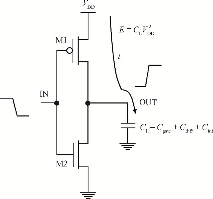
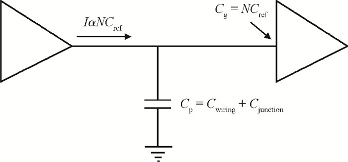
Fig. 1.
Load capacitance and its components.
SEMICONDUCTOR INTEGRATED CIRCUITS
Vijay Kumar Sharma and Manisha Pattanaik
Corresponding author: Vijay Kumar Sharma, Email: vijay.buland@gmail.com
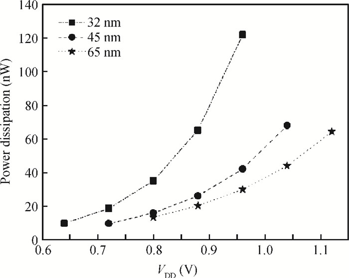
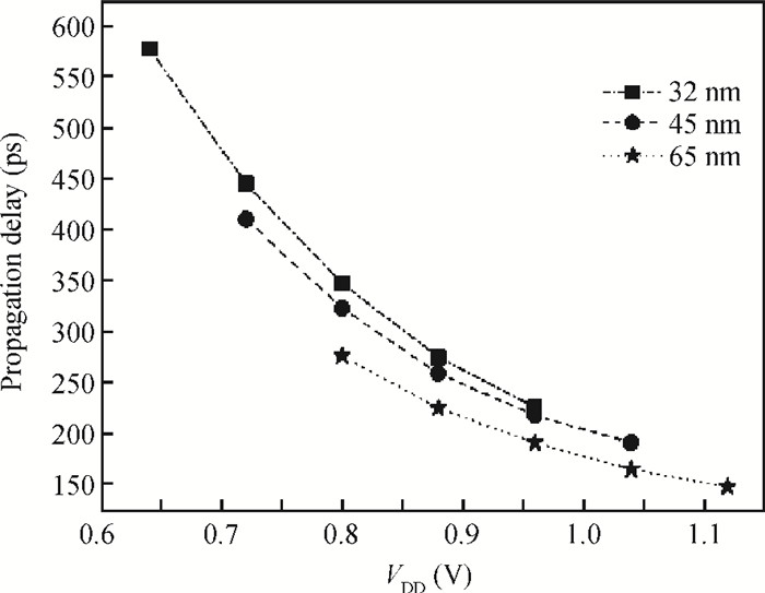
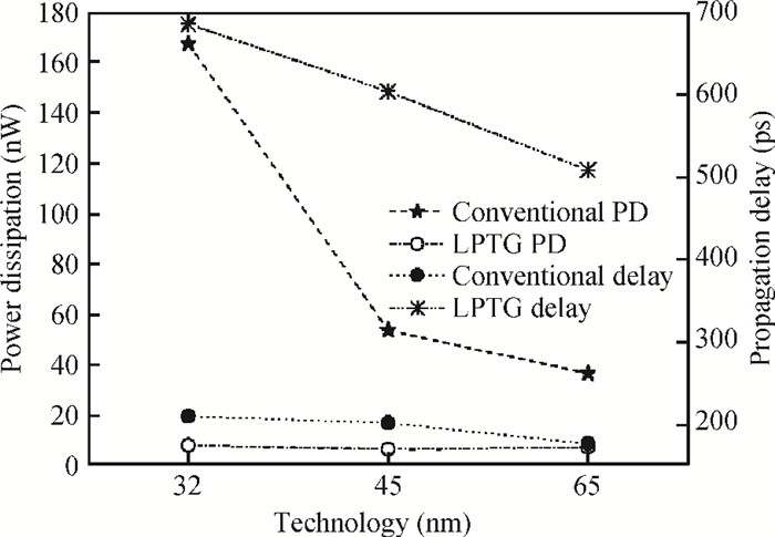
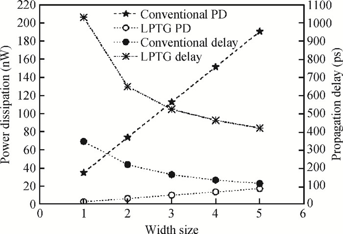
Abstract: Device scaling is an important part of the very large scale integration (VLSI) design to boost up the success path of VLSI industry, which results in denser and faster integration of the devices. As technology node moves towards the very deep submicron region, leakage current and circuit reliability become the key issues. Both are increasing with the new technology generation and affecting the performance of the overall logic circuit. The VLSI designers must keep the balance in power dissipation and the circuit's performance with scaling of the devices. In this paper, different scaling methods are studied first. These scaling methods are used to identify the effects of those scaling methods on the power dissipation and propagation delay of the CMOS buffer circuit. For mitigating the power dissipation in scaled devices, we have proposed a reliable leakage reduction low power transmission gate (LPTG) approach and tested it on complementary metal oxide semiconductor (CMOS) buffer circuit. All simulation results are taken on HSPICE tool with Berkeley predictive technology model (BPTM) BSIM4 bulk CMOS files. The LPTG CMOS buffer reduces 95.16% power dissipation with 84.20% improvement in figure of merit at 32 nm technology node. Various process, voltage and temperature variations are analyzed for proving the robustness of the proposed approach. Leakage current uncertainty decreases from 0.91 to 0.43 in the CMOS buffer circuit that causes large circuit reliability.
Key words: LPTG buffer, power dissipation, propagation delay, scaling, nanoscale CMOS, figure of merit
| [1] |
Agarwal A, Mukhopadhyay S, Raychowdhury A, et al. Leakage power analysis and reduction for nanoscale circuits. IEEE Micro, 2006, 26(2):68 doi: 10.1109/MM.2006.39
|
| [2] |
Liao W, He L, Lepak K M. Temperature and supply voltage aware performance and power modeling at microarchitecture level. IEEE Trans Computer-Aided Design of Integrated Circuits and Systems, 2005, 24(7):1042 doi: 10.1109/TCAD.2005.850860
|
| [3] |
Dhillon Y S, Diril A U, Chatterjee A, et al. Analysis and optimization of nanometer CMOS circuits for soft-error tolerance. IEEE Trans Very Large Scale Integration Syst, 2006, 14(5):514 doi: 10.1109/TVLSI.2006.876104
|
| [4] |
Wong H, Iwai H. On the scaling issues and high-κ replacement of ultrathin gate dielectrics for nanoscale MOS transistors. Microelectron Eng, 2006, 83(10):1867 doi: 10.1016/j.mee.2006.01.271
|
| [5] |
Lin C H, Haensch W, Oldiges P, et al. Modeling of width-quantization-induced variations in logic FinFETs for 22 nm and beyond. Digest of Technical Papers, Symposium on VLSI Technology, 2011:16
|
| [6] |
Kang S M, Leblebici Y. CMOS digital integrated circuits analysis and design. New Delhi:Tata McGraw-Hill, 2003 http://ci.nii.ac.jp/ncid/BA27828645
|
| [7] |
Islam A, Hasan M. Leakage characterization of 10T SRAM cell. IEEE Trans Electron Devices, 2012, 59(3):631 doi: 10.1109/TED.2011.2181387
|
| [8] |
Nayan A N, Yasuhiro T, Toshikazu S. LSI implementation of a low-power 4×4-bit array two-phase clocked adiabatic static CMOS logic multiplier. Microelectron J, 2012, 43(4):244 doi: 10.1016/j.mejo.2011.12.013
|
| [9] |
Elkamma A N, Vemuru S R. Scaling of serially-connected MOS transistors with constant area constraint. Midwest Symposium on Circuits and Systems, 2002:1515 http://ieeexplore.ieee.org/document/1187271/authors
|
| [10] |
Chandrakasan A P, Brodersen R W. Minimizing power consumption in CMOS circuits. Proc IEEE, 1995, 83(4):498 doi: 10.1109/5.371964
|
| [11] |
Guo X, Ipek E, Soyata T. Resistive computation:Avoiding the power wall with low-leakage, STT-MRAM based computing. International Symposium on Computer Architecture, 2012:371 http://www.cs.rochester.edu/~ipek/isca10.pdf
|
| [12] |
Ho Y, Chang C, Su C. Design of a subthreshold supply bootstrapped CMOS inverter based on an active leakage-current reduction technique. IEEE Trans Circuits Syst Ⅱ:Express Briefs, 2012, 59(1):55 doi: 10.1109/TCSII.2011.2174674
|
| [13] |
Sharma V K, Pattanaik M, Raj B. ONOFIC approach:low power high speed nanoscale VLSI circuits design. International Journal of Electronics, 2013, (in press) doi: 10.1080/00207217.2013.769186?scroll=top&needAccess=true&journalCode=tetn20
|
| [14] |
Wang J, Gong N, Hou L, et al. Leakage current, active power, and delay analysis of dynamic dual Vt CMOS circuits under P-V-T fluctuations. Microelectronics Reliability, 2011, 51(9):1498 https://www.ndsu.edu/pubweb/~nagong/index_files/journal/J4.pdf
|
| [15] |
Hanchate N, Ranganathan N. LECTOR:a technique for leakage reduction in CMOS circuits. IEEE Trans Very Large Scale Integration Syst, 2004, 12(2):196 doi: 10.1109/TVLSI.2003.821547
|


Article views: 26177 Times PDF downloads: 264 Times Cited by: 0 Times
Received: 15 February 2013 Revised: 20 March 2013 Online: Published: 01 September 2013
| Citation: |
Vijay Kumar Sharma, Manisha Pattanaik. VLSI scaling methods and low power CMOS buffer circuit[J]. Journal of Semiconductors, 2013, 34(9): 095001. doi: 10.1088/1674-4926/34/9/095001
****
V K Sharma, M Pattanaik. VLSI scaling methods and low power CMOS buffer circuit[J]. J. Semicond., 2013, 34(9): 095001. doi: 10.1088/1674-4926/34/9/095001.

|
| [1] |
Agarwal A, Mukhopadhyay S, Raychowdhury A, et al. Leakage power analysis and reduction for nanoscale circuits. IEEE Micro, 2006, 26(2):68 doi: 10.1109/MM.2006.39
|
| [2] |
Liao W, He L, Lepak K M. Temperature and supply voltage aware performance and power modeling at microarchitecture level. IEEE Trans Computer-Aided Design of Integrated Circuits and Systems, 2005, 24(7):1042 doi: 10.1109/TCAD.2005.850860
|
| [3] |
Dhillon Y S, Diril A U, Chatterjee A, et al. Analysis and optimization of nanometer CMOS circuits for soft-error tolerance. IEEE Trans Very Large Scale Integration Syst, 2006, 14(5):514 doi: 10.1109/TVLSI.2006.876104
|
| [4] |
Wong H, Iwai H. On the scaling issues and high-κ replacement of ultrathin gate dielectrics for nanoscale MOS transistors. Microelectron Eng, 2006, 83(10):1867 doi: 10.1016/j.mee.2006.01.271
|
| [5] |
Lin C H, Haensch W, Oldiges P, et al. Modeling of width-quantization-induced variations in logic FinFETs for 22 nm and beyond. Digest of Technical Papers, Symposium on VLSI Technology, 2011:16
|
| [6] |
Kang S M, Leblebici Y. CMOS digital integrated circuits analysis and design. New Delhi:Tata McGraw-Hill, 2003 http://ci.nii.ac.jp/ncid/BA27828645
|
| [7] |
Islam A, Hasan M. Leakage characterization of 10T SRAM cell. IEEE Trans Electron Devices, 2012, 59(3):631 doi: 10.1109/TED.2011.2181387
|
| [8] |
Nayan A N, Yasuhiro T, Toshikazu S. LSI implementation of a low-power 4×4-bit array two-phase clocked adiabatic static CMOS logic multiplier. Microelectron J, 2012, 43(4):244 doi: 10.1016/j.mejo.2011.12.013
|
| [9] |
Elkamma A N, Vemuru S R. Scaling of serially-connected MOS transistors with constant area constraint. Midwest Symposium on Circuits and Systems, 2002:1515 http://ieeexplore.ieee.org/document/1187271/authors
|
| [10] |
Chandrakasan A P, Brodersen R W. Minimizing power consumption in CMOS circuits. Proc IEEE, 1995, 83(4):498 doi: 10.1109/5.371964
|
| [11] |
Guo X, Ipek E, Soyata T. Resistive computation:Avoiding the power wall with low-leakage, STT-MRAM based computing. International Symposium on Computer Architecture, 2012:371 http://www.cs.rochester.edu/~ipek/isca10.pdf
|
| [12] |
Ho Y, Chang C, Su C. Design of a subthreshold supply bootstrapped CMOS inverter based on an active leakage-current reduction technique. IEEE Trans Circuits Syst Ⅱ:Express Briefs, 2012, 59(1):55 doi: 10.1109/TCSII.2011.2174674
|
| [13] |
Sharma V K, Pattanaik M, Raj B. ONOFIC approach:low power high speed nanoscale VLSI circuits design. International Journal of Electronics, 2013, (in press) doi: 10.1080/00207217.2013.769186?scroll=top&needAccess=true&journalCode=tetn20
|
| [14] |
Wang J, Gong N, Hou L, et al. Leakage current, active power, and delay analysis of dynamic dual Vt CMOS circuits under P-V-T fluctuations. Microelectronics Reliability, 2011, 51(9):1498 https://www.ndsu.edu/pubweb/~nagong/index_files/journal/J4.pdf
|
| [15] |
Hanchate N, Ranganathan N. LECTOR:a technique for leakage reduction in CMOS circuits. IEEE Trans Very Large Scale Integration Syst, 2004, 12(2):196 doi: 10.1109/TVLSI.2003.821547
|

 WeChat ID
Journal of Semiconductors © 2017 All Rights Reserved 京ICP备05085259号-2

 DownLoad: