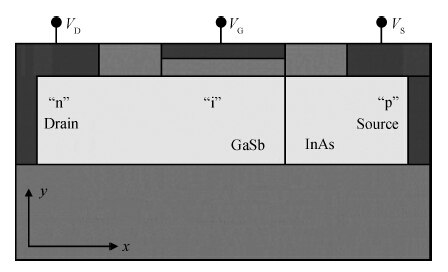
P K Asthana. High performance 20 nm GaSb/InAs junctionless tunnel field effect transistor for low power supply[J]. J. Semicond., 2015, 36(2): 024003. doi: 10.1088/1674-4926/36/2/024003.
Abstract: We present a GaSb/InAs junctionless tunnel FET and investigate its static device characteristics. The proposed structure presents tremendous performance at a very low supply voltage of 0.4 V. The key idea is to the present device architecture, which can be exploited as a digital switching device for sub 20 nm technology. Numerical simulations resulted in an IOFF of ~8 × 10-17 A/μm, ION of ~ 9 μA/μm, ION/IOFF of ~1 × 10¹¹, subthreshold slope of 9.33 mV/dec and DIBL of ~ 87 mV/V for GaSb/InAs JLTFET at a temperature of 300 K, gate length of 20 nm, HfO2 gate dielectric thickness of 2 nm, film thickness of 10 nm, low-k spacer thickness of 10 nm and VDD of 0.4 V.
Key words: band tunneling (BTBT), tunnel field effect transistor (TFET), junctionless tunnel field effect transistor (JLTFET), ION/IOFF ratio, low power, digital switching
Abstract: We present a GaSb/InAs junctionless tunnel FET and investigate its static device characteristics. The proposed structure presents tremendous performance at a very low supply voltage of 0.4 V. The key idea is to the present device architecture, which can be exploited as a digital switching device for sub 20 nm technology. Numerical simulations resulted in an IOFF of ~8 × 10-17 A/μm, ION of ~ 9 μA/μm, ION/IOFF of ~1 × 10¹¹, subthreshold slope of 9.33 mV/dec and DIBL of ~ 87 mV/V for GaSb/InAs JLTFET at a temperature of 300 K, gate length of 20 nm, HfO2 gate dielectric thickness of 2 nm, film thickness of 10 nm, low-k spacer thickness of 10 nm and VDD of 0.4 V.
Key words:
band tunneling (BTBT), tunnel field effect transistor (TFET), junctionless tunnel field effect transistor (JLTFET), ION/IOFF ratio, low power, digital switching
References:
[1] |
Dallmann D A, Shenai K. Scaling constraints imposed by self-heating in submicron SO1 MOSFET's[J]. IEEE Trans Electron Devices, 1995, 42(3): 489. |
[2] |
Chan T Y, Chen J, Ko P K. The impact of gate-induced drain leakage current on MOSFET scaling[J]. International Electron Devices Meeting, 1987, 31. |
[3] |
Suzuki K, Tanaka T, Tosaka Y. Scaling theory for double-gate SO1 MOSFET's[J]. IEEE Trans Electron Devices, 1993, 40(12): 2326. |
[4] |
Bohr M. A 30 year retrospective on Dennard's MOSFET scaling paper[J]. IEEE Solid-State Circuits Society Newsletter, 2007, 12(1): 11. |
[5] |
Frank D J, Taur Y, Wong H S P. Generalized scale length for two-dimensional effects in MOSFET's[J]. IEEE Electron Device Lett, 1998, 19(10): 385. |
[6] |
Reddy G V, Kumar M J. A new dual-material double-gate (DMDG) nanoscale SOI MOSFET——two-dimensional analytical modeling and simulation[J]. IEEE Trans Nanotech, 2005, 4(2): 260. |
[7] |
Critchlow D L. MOSFET scaling-the driver of VLSI technology[J]. Proc IEEE, 1999, 87(4): 659. |
[8] |
Frank D J, Dennard R H, Nowak E. Device scaling limits of Si MOSFETs and their application dependencies[J]. Proc IEEE, 2001, 89(3): 259. |
[9] |
Hu C. Future CMOS scaling and reliability[J]. Proc IEEE, 1993, 81(5): 682. |
[10] |
Li M, Yeo K H, Suk S D. Sub-10 nm gate-all-around CMOS nanowire transistors on bulk Si substrate[J]. Symposium on VLSI Technology, 2009: 94. |
[11] |
Gautam R, Saxena M, Gupta R S. Gate-all-around nanowire MOSFET with catalytic metal gate for gas sensing applications[J]. IEEE Trans Nanotech, 2013, 12(6): 939. |
[12] |
Song Y, Zhang C, Dowdy R. III—V junctionless gate-all-around nanowire MOSFETs for high linearity low power applications[J]. IEEE Electron Device Lett, 2014, 35(3): 324. |
[13] |
Coquand R, Cassé M, Barraud S. Strain-induced performance enhancement of tri-gate and omega-gate nanowire FETs scaled down to 10 nm width[J]. IEEE Symposium on VLSI Technology Digest of Technical Papers, 2012: 13. |
[14] |
Ray B, Mahapatra S. A new threshold voltage model for omega gate cylindrical nanowire transistor[J]. 21st International Conference on VLSI Design, 2008: 447. |
[15] |
Yu Z, Li L, Zhang L. Compact modeling for gate-all-around nanowire tunneling FETs (GAA NW-tFETs)[J]. IEEE 11th International Conference on Solid-State and Integrated Circuit Technology (ICSICT), 2012: 1. |
[16] |
Yang B, Buddharaju K D, Teo S H G. Vertical silicon-nanowire formation and gate-all-around MOSFET[J]. IEEE Electron Device Lett, 2008, 29(7): 791. |
[17] |
Larrieu G, Han X L. Vertical nanowire array-based field effect transistors for ultimate scaling[J]. Nanoscale, 2013, 5: 2437. |
[18] |
Robinson J T, Jorgolli M, Shalek A K. Vertical nanowire electrode arrays as a scalable platform for intracellular interfacing to neuronal circuits[J]. Nature Nanotechnol, 2012, 7: 180. |
[19] |
Simoe E, Claeys C. DC characteristics of gate-all-around (GAA) silicon-on-insulator MOSFETs at cryogenic temperatures[J]. Journal de Physique IV, Colloque C6, Supplkment au Journal de Physique III, 1994, 4: 51. |
[20] |
Gandhi R, Chen Z, Singh N. CMOS-compatible vertical-silicon-nanowire gate-all-around p-type tunneling FETs with ≤qslant 50-mV/decade subthreshold swing[J]. IEEE Electron Device Lett, 2011, 32(11): 1504. |
[21] |
Tomioka K, Yoshimura M, Fukui T. A III—V nanowire channel on silicon for high-performance vertical transistors[J]. Nature, 2012, 488: 189. |
[22] |
Sacchetio D, Ben-Jamaal M H, De Michelil G. Fabrication and characterization of vertically stacked gate-all-around Si nanowire FET arrays[J]. Proc of the 39th European Solid-State Dev Res Conf (ESSDERC), 2009. |
[23] |
Shen N, Le T T, Yu H Y. Fabrication and characterization of poly-Si vertical nanowire thin film transistor[J]. World Acad of Sci, Eng and Tech, 2011: 57. |
[24] |
Le T T, Yu H Y, Sun Y. High-performance poly-Si vertical nanowire thin-film transistor and the inverter demonstration[J]. IEEE Electron Device Lett, 2011, 32(6): 770. |
[25] |
Lilienfeld J E. Method and apparatus for controlling electric current[J]. US Patent, No, 1920. |
[26] |
Colinge J P, Lee C W, Afzalian A. Nanowire transistors without junctions[J]. Nature Nanotechnol, 2010, 5(3): 225. |
[27] |
Lee C W, Afzalian A, Akhavan N D. Junctionless multigate field-effect transistor[J]. Appl Phys Lett, 2009, 94(5): 053511. |
[28] |
Gundapaneni S, Ganguly S, Kottantharayil A. Enhanced electrostatic integrity of short channel junctionless transistor with high-k spacers[J]. IEEE Electron Device Lett, 2011, 32(10): 1325. |
[29] |
Lee C W, Ferain I, Afzalian A. Performance estimation of junctionless multigate transistors[J]. Solid-State Electron, 2010, 54(2): 97. |
[30] |
Gundapaneni S, Ganguly S, Kottantharayil A. Bulk planar junctionless transistor (BPJLT): an attractive device alternative for scaling[J]. IEEE Electron Device Lett, 2011, 32(3): 261. |
[31] |
Kranti A, Lee C W, Ferain I. Junctionless nanowire transistor: properties and design guidelines[J]. Proc 34th IEEE Eur Solid-State Device Res Conf, 2010: 357. |
[32] |
Choi S J, Moon D I, Kim S. Nonvolatile memory by all-around-gate junctionless transistor composed of silicon nanowire on bulk substrate[J]. IEEE Electron Device Lett, 2011, 32(5): 602. |
[33] |
Lee C W, Yan R, Ferain I. Nanowire zero-capacitor DRAM transistors with and without junctions[J]. Proc 10th IEEE-NANO, 2010: 242. |
[34] |
Kranti A, Lee C, Ferain I. Junctionless 6T SRAM cell[J]. IET Electron Lett, 2010, 46(22): 1491. |
[35] |
Ghosh B, Akram M W. Junctionless tunnel field effect transistor[J]. IEEE Electron Device Lett, 2013, 34(5): 584. |
[36] |
Asthana P K, Ghosh B, Goswami Y. High-speed and low-power ultradeep-submicrometer III—V heterojunctionless tunnel field-effect transistor[J]. IEEE Trans Electron Devices, 2014, 61(2): 479. |
[37] |
Asthana P K, Ghosh B, Rahi S B. Optimal design of high performance H-JLTFET using HfO2 as gate dielectric for ultra low power applications[J]. RSC Adv, 2014, 43(4): 22803. |
[38] |
Goswami, Asthana, Pranav. Junctionless tunnel field effect transistor with enhanced performance using III—V semiconductor[J]. Journal of Low Power Electronics, 2013, 9(4): 496. |
[39] |
Goswami Y, Ghosh B, Asthana P K. Analog performance of Si junctionless tunnel field effect transistor and its improvisation using III—V semiconductor[J]. RSC Adv, 2014, 21(4): 10761. |
[40] |
Bal P, Akram M W, Mondal P. Performance estimation of sub-30 nm junctionless tunnel FET (JLTFET)[J]. J Comput Electron, 2013, 12: 782. |
[41] |
Koswatta S O, Koester S J, Hanench W. On the possibility of obtaining MOSFET-like performance and sub-60 mV/dec swing in 1-D broken gap tunnel transistors[J]. IEEE Trans Electron Devices, 2010, 57(12): 3222. |
[42] |
Khan U, Ghosh B, Akaram M W. Effect of self heating on selective buried oxide and silicon on insulator based junction less transistors[J]. Journal of Low Power Electronics, 2013, 9: 1. |
[43] |
Koswatta S O, Lundstram M S, Nikonov D E. Performance comparison between p—i—n tunneling transistors and conventional MOSFETs[J]. IEEE Trans Electron Devices, 2009, 56(3): 456. |
[44] |
Ionescu A M, Riel H. Tunnel field-effect transistors as energy-efficient electronic switches[J]. Nature, 2011, 479: 329. |
[45] |
Boucart K, Ionesscu A M. Double-gate tunnel FET with high-k gate dielectric[J]. IEEE Trans Electron Devices, 2007, 54(7): 1725. |
[46] |
Bhuwalka K K, Born M, Schinder M. P-channel tunnel FET transistors down to sub-50 nm channel lengths[J]. J Appl Phys, 2006, 45(4): 3106. |
[47] |
Kane E O. Zenner tunneling in semiconductor[J]. J Phys Chem Solids, 1960, 12(2): 181. |
[48] |
Mammilla B K, Nair S, Mishra R. A III—V group tunnel FETs with good switching characteristics and their circuit performance[J]. International Journal of Electronics Communication and Computer Technology (IJECCT), 2011, 1(2): 26. |
[49] |
Hurkx G A M, Klasssen D B M, Knuvers P G. A new recombination model for device simulation including tunnelling[J]. IEEE Trans Electron Devices, 1992, 39(2): 331. |
[50] |
Taur Y, Ning T H. Fundamentals of modern VLSI devices[J]. Cambridge, UK: Cambridge University Press, 1998. |
[51] |
Eisberg R, Resnick R. Quantum physics of atoms, molecules, solids, nuclei and particles[J]. 2nd ed. Wiley Student Edition, 2012. |
[52] |
Zhou G, Li R, Vasen T. Novel gate-recessed vertical InAs/GaSb TFETs with record high ION of 180 μ A/μ m at VDS = 0.5 V[J]. IEEE International Electron Devices Meeting (IEDM), 2013. |
[53] |
Li R, Lu Y, Chae S D. InAs/AlGaSb heterojunction tunnel field-effect transistor with tunnelling in-line with the gate field[J]. Physica Status Solidi C, 2012, 9(2): 389. |
[54] |
Borg B M, Dick K A, Ganjipou B. InAs/GaSb heterostructure nanowires for tunnel field-effect transistors[J]. Nano Lett, 2010, 10(10): 4080. |
[55] |
Dey A W, Borg B M, Ganjipour B. High-current GaSb/InAs(Sb) nanowire tunnel field-effect transistors[J]. IEEE Electron Device Lett, 2013, 34(2): 211. |
[56] |
Schmid H, Moselund K E, Björk M T. Fabrication of vertical InAs—Si heterojunction tunnel field effect transistors[J]. Device Research Conference (DRC), 2011, 69: 181. |
[57] |
Yang R, Li G H, Xu Y Z. Two dimensional device simulation and fabrication of mesa SOI vertical dual carrier field effect transistor with effective channel length of 30 nm for switching ASIC and SOC[J]. 6th ASICON, 2005, 2: 1102. |
[58] |
Anderson R L. Experiments on Ge—GaAs heterojunctions[J]. Solid-State Electron, 1962, 5: 341. |
[59] |
Spicer W E, Lindau I, Skeath P. Unified defect model and beyond[J]. J Vac Sci Technol, 1980, 17: 1019. |
[60] |
Hinkle C L, Sonnet A M, Vogel E M. GaAs interfacial self-cleaning by atomic layer deposition[J]. Appl Phys Lett, 2008, 92: 071901. |
[61] |
Ye P D, Wilk G D, Kwo J. GaAs MOSFET with oxide gate dielectric grown by atomic layer deposition[J]. IEEE Electron Device Lett, 2003, 24: 209. |
[62] | |
[63] |
Schenk A. A model for the field and temperature dependence of SRH lifetimes in silicon[J]. Solid-State Electron, 1992, 35(11): 1585. |
[64] |
Hansch W, Vogelsang T, Kirchner R. Carrier transport near the Si/SiO2 interface of a MOSFET[J]. Solid-State Electron, 1989, 32(10): 839. |
[65] |
Van Zeghbroeck B. Principles of semiconductor devices[J]. . |
[66] |
Kumar M J, Siva M. The ground plane in buried oxide for controlling short-channel effects in nano scale SOI MOSFETs[J]. IEEE Trans Electron Devices, 2008, 55: 1554. |
[67] |
ITRS, http://www. itrs[J]. net accessed on 21 June, 2013. |
[68] |
Hu C C. Modern semiconductor devices for integrated circuits[J]. 1st ed. Pearson India, 2010. |
P K Asthana. High performance 20 nm GaSb/InAs junctionless tunnel field effect transistor for low power supply[J]. J. Semicond., 2015, 36(2): 024003. doi: 10.1088/1674-4926/36/2/024003.
Article views: 791 Times PDF downloads: 9 Times Cited by: 0 Times
Manuscript received: 20 July 2014 Manuscript revised: Online: Published: 01 February 2015
Journal of Semiconductors © 2017 All Rights Reserved