


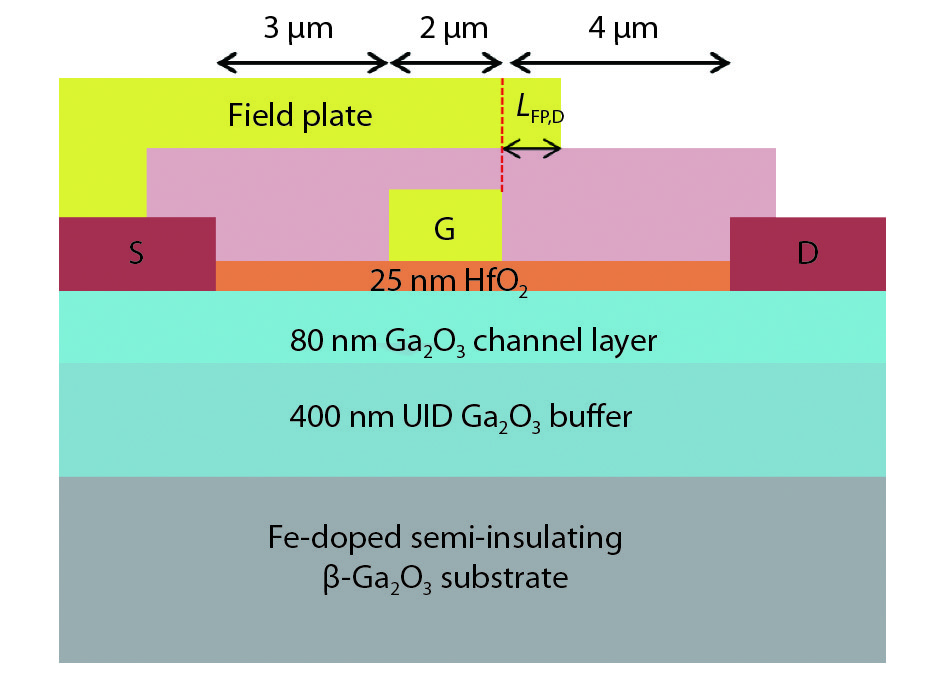
Fig. 1.
(Color online) Schematic cross section of the fabricated Ga2O3 MOSFET with Lgd of 4 μm.
ARTICLES
Yuanjie Lü, Xubo Song, Zezhao He, Yuangang Wang, Xin Tan, Shixiong Liang, Cui Wei, Xingye Zhou and Zhihong Feng
Corresponding author: Xingye Zhou, Email: xyzhoufly@163.com; Zhihong Feng, ga917vv@163.com
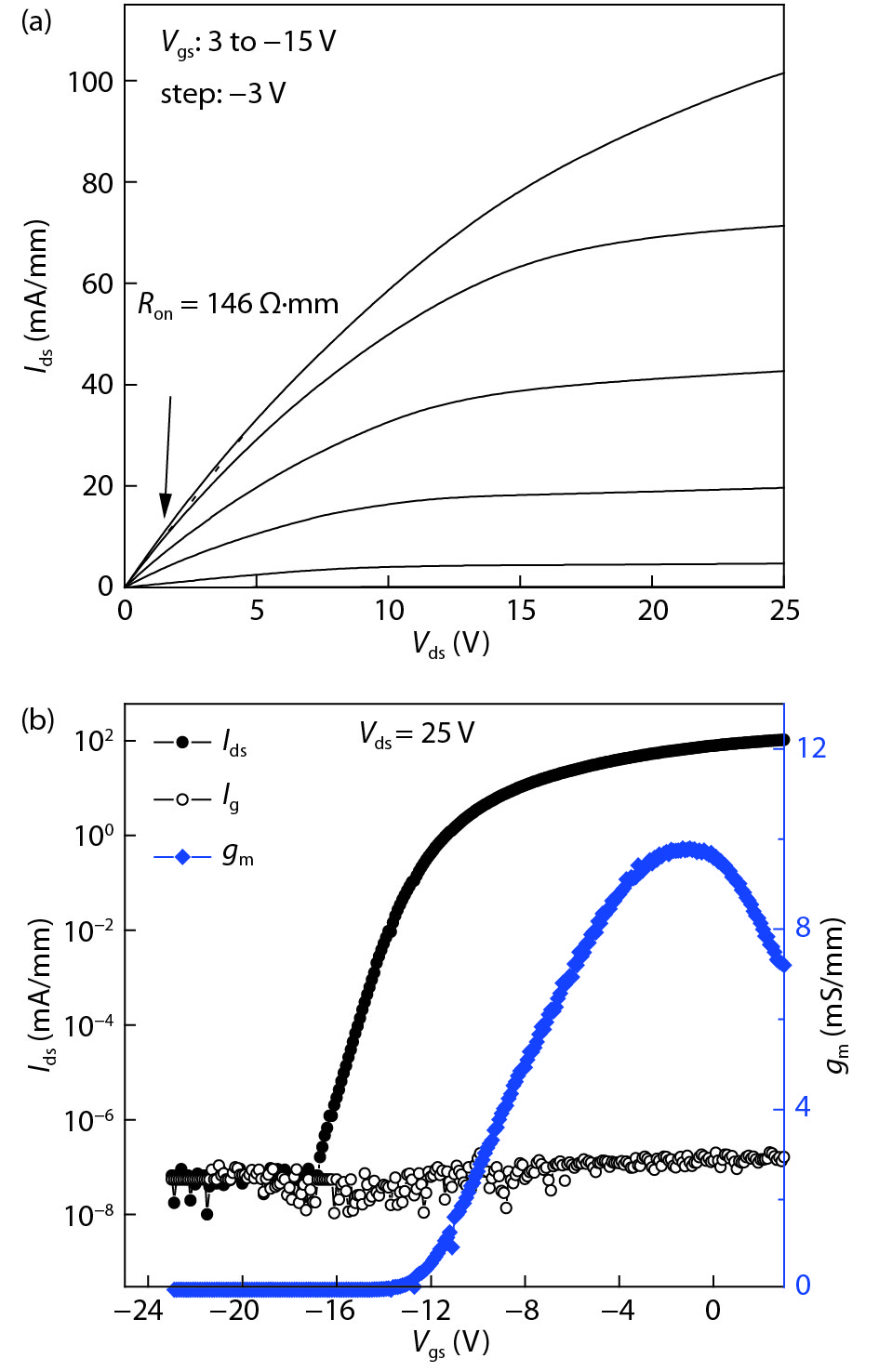
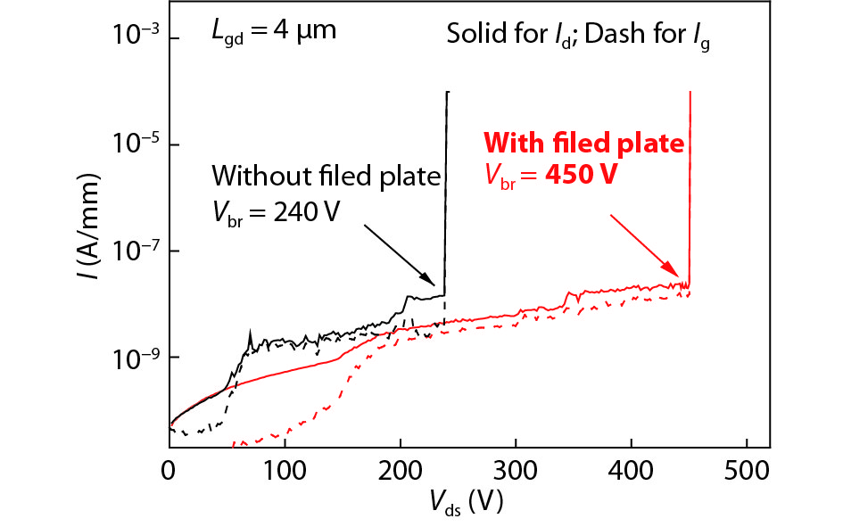
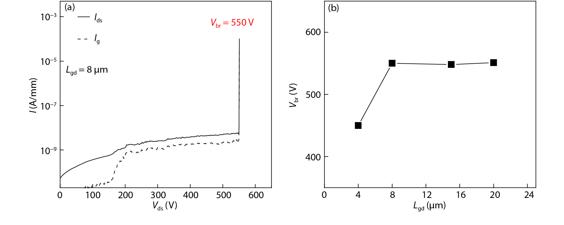
Abstract: Ga2O3 metal–oxide–semiconductor field-effect transistors (MOSFETs) with high-breakdown characteristics were fabricated on a homoepitaxial n-typed β-Ga2O3 film, which was grown by metal organic chemical vapor deposition (MOCVD) on an Fe-doped semi-insulating (010) Ga2O3 substrate. The structure consisted of a 400 nm unintentionally doped (UID) Ga2O3 buffer layer and an 80 nm Si-doped channel layer. A high k HfO2 gate dielectric film formed by atomic layer deposition was employed to reduce the gate leakage. Moreover, a source-connected field plate was introduced to enhance the breakdown characteristics. The drain saturation current density of the fabricated device reached 101 mA/mm at Vgs of 3 V. The off-state current was as low as 7.1 × 10⁻¹¹ A/mm, and the drain current ION/IOFF ratio reached 109. The transistors exhibited three-terminal off-state breakdown voltages of 450 and 550 V, corresponding to gate-to-drain spacing of 4 and 8 μm, respectively.
Key words: Ga2O3, MOSFET, breakdown voltage, filed plate
| [1] |
Zhang H Z, Wang L J, Xia C T, et al. Research progress of wide-gap semiconductor β-Ga2O3 single crystal. J Synth Cryst, 2015, 44: 2943
|
| [2] |
Gogova D, Wagner G, Balndini M, et al. Structural properties of Si-doped β-Ga2O3 layers grown by MOVPE. J Cryst Growth, 2014, 401: 665 doi: 10.1016/j.jcrysgro.2013.11.056
|
| [3] |
Higashiwaki M, Sasali K, Kuramata T, et al. Depletion-mode Ga2O3 metal–oxide–semiconductor field-effect transistors on β-Ga2O3 (010) substrates and temperature dependence of their device characteristics. Appl Phys Lett, 2013, 103: 123511 doi: 10.1063/1.4821858
|
| [4] |
Wong M H, Sasaki K, Kuramata A, et al. Field-plated Ga2O3 MOSFET with a breakdown voltage of over 750V. IEEE Electron Device Lett, 2016, 37: 212 doi: 10.1109/LED.2015.2512279
|
| [5] |
Zhou H, Maize K, Qiu G, et al. β-Ga2O3 on insulator field-effect transistors with drain currents exceeding 1.5 A/mm and their self-heating effect. Appl Phys Lett, 2017, 111: 092102 doi: 10.1063/1.5000735
|
| [6] |
Han T T, Lv Y J, Liu P, et al. Research and Fabrication of Ga2O3 MOSFET device with HfO2 gate dielectric. Semicond Technol, 2018, 43: 177
|
| [7] |
Lv Y J, Mo J H, Song X B, et al. Influence of gate recess on the electronic characteristics of β-Ga2O3 MOSFETs. Superlattices Microstruct, 2018, 117:132 doi: 10.1016/j.spmi.2018.03.013
|


Article views: 6109 Times PDF downloads: 315 Times Cited by: 0 Times
Received: 07 June 2018 Revised: 05 July 2018 Online: Uncorrected proof: 13 September 2018Published: 07 January 2019
| Citation: |
Yuanjie Lü, Xubo Song, Zezhao He, Yuangang Wang, Xin Tan, Shixiong Liang, Cui Wei, Xingye Zhou, Zhihong Feng. Source-field-plated Ga2O3 MOSFET with a breakdown voltage of 550 V[J]. Journal of Semiconductors, 2019, 40(1): 012803. doi: 10.1088/1674-4926/40/1/012803
****
Y J Lü, X B Song, Z Z He, Y G Wang, X Tan, S X Liang, C Wei, X Y Zhou, Z H Feng, Source-field-plated Ga2O3 MOSFET with a breakdown voltage of 550 V[J]. J. Semicond., 2019, 40(1): 012803. doi: 10.1088/1674-4926/40/1/012803.

|
| [1] |
Zhang H Z, Wang L J, Xia C T, et al. Research progress of wide-gap semiconductor β-Ga2O3 single crystal. J Synth Cryst, 2015, 44: 2943
|
| [2] |
Gogova D, Wagner G, Balndini M, et al. Structural properties of Si-doped β-Ga2O3 layers grown by MOVPE. J Cryst Growth, 2014, 401: 665 doi: 10.1016/j.jcrysgro.2013.11.056
|
| [3] |
Higashiwaki M, Sasali K, Kuramata T, et al. Depletion-mode Ga2O3 metal–oxide–semiconductor field-effect transistors on β-Ga2O3 (010) substrates and temperature dependence of their device characteristics. Appl Phys Lett, 2013, 103: 123511 doi: 10.1063/1.4821858
|
| [4] |
Wong M H, Sasaki K, Kuramata A, et al. Field-plated Ga2O3 MOSFET with a breakdown voltage of over 750V. IEEE Electron Device Lett, 2016, 37: 212 doi: 10.1109/LED.2015.2512279
|
| [5] |
Zhou H, Maize K, Qiu G, et al. β-Ga2O3 on insulator field-effect transistors with drain currents exceeding 1.5 A/mm and their self-heating effect. Appl Phys Lett, 2017, 111: 092102 doi: 10.1063/1.5000735
|
| [6] |
Han T T, Lv Y J, Liu P, et al. Research and Fabrication of Ga2O3 MOSFET device with HfO2 gate dielectric. Semicond Technol, 2018, 43: 177
|
| [7] |
Lv Y J, Mo J H, Song X B, et al. Influence of gate recess on the electronic characteristics of β-Ga2O3 MOSFETs. Superlattices Microstruct, 2018, 117:132 doi: 10.1016/j.spmi.2018.03.013
|

 WeChat ID
Journal of Semiconductors © 2017 All Rights Reserved 京ICP备05085259号-2

 DownLoad:

