J. Semicond. > 2019, Volume 40 > Issue 5 > 050301

COMMENTS AND OPINIONS

Precision photonic integration for future large-scale photonic integrated circuits

Xiangfei Chen

+ Author Affiliations
DOI: 10.1088/1674-4926/40/5/050301

PDF

Turn off MathJax

Abstract: Since the proposal of the concept of photonic integrated circuits (PICs), tremendous progress has been made. In 2005, Infinera Corp. rolled out the first commercial PICs, in which hundreds of optical functions were integrated onto a small form factor chip for wavelength division multiplexing (WDM) systems[1], then a monolithically integrated 10 × 10 Gb/s WDM chip has been demonstrated, the channel number is ten[2]. Like ICs, large-scale PICs (LS-PICs) will be sure to be pursued. However, there are still some general challenges associated with LS-PICs. The challenges for III–V (mainly InP) PICs is the semiconductor process, which is not mature for LS-PICs. Up to now, the channel number in commercial III–V WDM PICs by Infinera is still about ten or less. For silicon photonics, the challenge is the silicon based light source. The low cost and mature solution for silicon lasers is still unavailable and only 4 × 25 Gb/s PICs are deployed by Intel Corp. after 18-year R&D investment. Thus it is still unavailable for practical LS-PICs in the present times.

Why need precision photonic integration? Of the issues indicated above, another critical issue is how to increase the integration density at a very low cost. For dense WDM (DWDM), the standard wavelength spacing is 100 GHz or ~ 0.8 nm around 1550 nm. In order to produce the 0.8 nm wavelength difference, the structural variation in grating pitch or ring radius etc. could be as small as ~ 0.13 nm, which is near the size of a hydrogen atom. In future LS-PICs, there may be many wavelength sensitive components and their adjustment is realized by the change of the temperature. Because the maximum wavelength deviation may be as large as several nanometers, the maximum temperature change may be several tens of degrees, which will be leading a very low yield in LS-PICs. Therefore, precision wavelength control will be necessary for general LS-PICs. For example, multi-wavelength laser arrays (MLAs) with a high channel count are considered to be an engine of LS-PICs, but high-volume production of MLAs with accurate wavelength control and low manufacturing cost still remains a huge challenge. Currently, the distributed feedback (DFB) lasers used in MLAs are fabricated using electron beam lithography (EBL), which offers from high resolution fabrication but low throughput because of the long writing time[3]. It is also well-known that EBL suffers from drawbacks such as blanking or deflection errors and shaping errors. Very few references have discussed the non-uniformity of the wavelength spacing of the devices fabricated using EBL. In Ref. [4], it is shown that using EBL, only 35% lasers have a wavelength variation of less than ± 0.2 nm. Ref. [5] shows that the error associated with the EBL process may be as large as 3 nm. In Ref. [6], when the difference between the two rings is only about 0.4 nm, the optical response is completely different. This shows that although the optical components are much larger than transistors in ICs, the higher process precision control is necessary for PICs. We can call this as precision photonic integrated circuits (precision PICs). Precision PICs means the resonance wavelength (channel) spacing will be controlled precisely.

What is reconstruction-equivalent-chirp (REC) technique for semiconductor laser and laser array? REC technique, which is first proposed by us, is a simple technique that only sampled Bragg grating (SBG) is used to design and fabricate lasers and laser arrays with complex grating structures. Through changing the sampling pattern, equivalent chirp (continuous change) or equivalent shift (discrete change) of the sub-gratings (Fourier components) in the SBG can be produced. The Bragg wavelengths of the sub-gratings can also be changed with the sampling period. Thus various sub-gratings with complex structures can be obtained by pre-designing the sampling pattern. Sampling period is usually several micrometers, which can be formed by using normal photolithography. Combined the reconstruction algorithm for desired optical response, the arbitrary grating profile (chirp/ shift) can be equivalently obtained by sampled grating with μm-level photolithography. That is why such a technique is called REC technique. The REC technique and its applications in semiconductor lasers have been illustrated in a number of papers[79] . The most important advantage of REC technique is its precision in wavelength control. Ref. [9] shows the error tolerance of the wavelength precision is largely relaxed by at least 100 times.

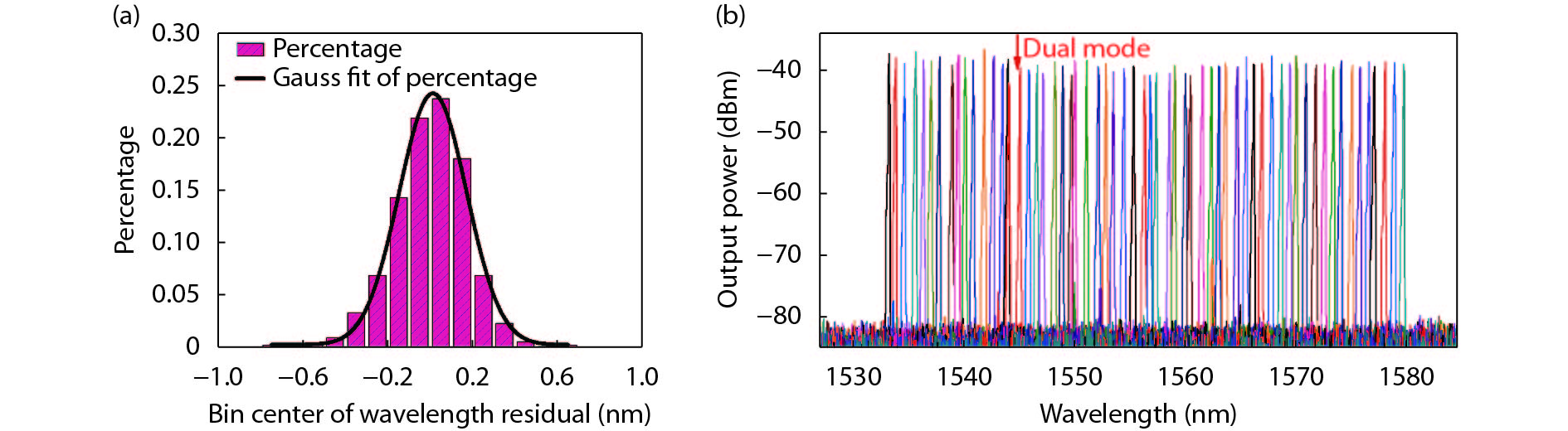
In Ref. [10], 60-wavelength DFB laser arrays with a π-equivalent phase shift (π-EPS) were designed and fabricated in two wafers. For all the laser arrays, the mean lasing wavelength residuals of 83.3% of the lasers are within ± 0.20 nm, and 93.5% are within ± 0.30 nm. Lasers with a wavelength deviation of > 0.50 nm are less than 1.0% of the total laser count. The single-longitudinal-mode (SLM) yield of lasers from the seven arrays are 98.3%, 100%, 100%, 100%, 98.3%, 93.3% and 100% respectively.

As shown in Fig. 1, the standarddeviationis 0.159 nm, which means 68.26% of the laser wavelengths are lied within ± 0.159 nm. The detailed lasing spectrum of one array was randomly selected. Its wavelength spacing is 0.8 nm.

Figure  1.  (Color online) (a) Frequency count of wavelength residual (871 lasers) and (b) measured lasing spectra of one 60-channel array.

From the above experimental results, it can be seen that low-cost high-channel-count and high precision channel spacing MLAs can be obtained by REC technique. It also implies that the two great obstacles to manufacture MLAs for very-large-scale PICs, namely poor wavelength accuracy and the low yield, which have impeded progress for nearly three decades, have been essentially overcome.

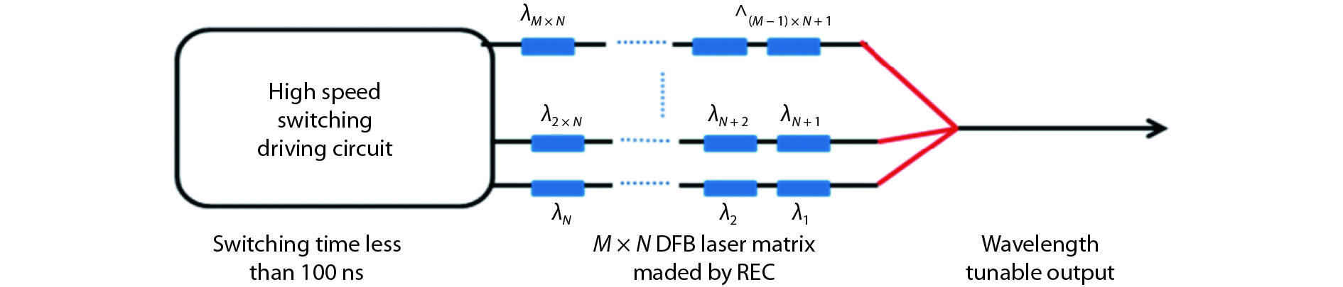
Typical applications? Fast tunable lasers with switching time less than one microsecond or even tens of nanoseconds (ultra-fast) are key components in high-speed smart networks or software defined networks (SDNs). The wavelength of the Vernier effect based tunable lasers can in principle be switched from one wavelength to another by tuning the currents. However, it comes with the change in heat dissipation and the thermal relaxation takes quite some time. Moreover, the thermal settling may cause mode hoping, which implies large deviations from the target wavelength. Thus Vernier effect based tunable lasers should be very difficult to be commercialized as fast tunable lasers. The other tunable laser with fast tuning speed is demonstrated by the tunable distributed amplification distributed feedback (TDA-DFB) principle[11], which is needed to examine in actual applications. It should be mentioned that the fabrication of TDA-DFB lasers is much more complex than Vernier effect based tunable lasers and the yield may be a problem, thus making the module very expensive.

An effective and low-cost method is to integrate multi-wavelength laser array (MLA) and switch between wavelengths by turning on/off individual lasers. The DFB lasers are very stable against temperature variations and the speed of electronics is only a few nanoseconds, making it possible to stabilize the wavelength within tens of nanoseconds. The proposed method is an M × N DFB laser matrix shown in Fig. 2. It can cover wide tuning range and the wavelength can be switched quickly by turning on/off individual lasers using high speed switching driving circuit. Because for a wideband fast tunable laser, there are at least 40-wavlength array, the precision PICs will be very important.

Figure  2.  (Color online) Schematic of an M × N DFB laser matrix with high speed switching driver circuit.

Possible way for LS-PICs based on precision PICs and photonic wire bonding?

Because up to now, both the semiconductor processes and the silicon lasers are very difficult for commercial LS-PICs, another possible way should be pursued, Photonic wire bonding (PWB) is a technique developed at the Karlsruhe Institute of Technology (KIT) of Germany in which photonic waveguides are written with an ultrafast laser into a photoresist material via two-photon lithography[12].

The combination of LS precision REC laser arrays and PWB may is a good way to LS-PICs, as Fig. 3 shows. The modulators and passive waveguides can be made based on silicon photonics.

Figure  3.  (Color online) Schematic of an LS-PICs based on the combination of LS precision REC laser arrays and PWB.

Ruiqin Jin

Ruiqin Jin is a senior editor of Journal of Semiconductors.


[1]
Nagarajan R, Joyner C H, Schneider R P, et al. Large-scale photonic integrated circuits. IEEE Journal of Selected Topics in Quantum Electronics, 2005, 11(1): 50 doi: 10.1109/JSTQE.2004.841721
[2]
Welch D F, Kish F A, Nagarajan R, et al. The realization of large-scale photonic integrated circuits and the associated impact on fiber-optic communication systems. Journal of lightwave technology, 2006, 24(12): 4674 doi: 10.1109/JLT.2006.885769
[3]
Koch T L, Koren U. Semiconductor photonic integrated circuits. IEEE Journal of Quantum Electronics, 1991, 27(3): 641 doi: 10.1109/3.81373
[4]
Lee T P, Zah C E, Bhat R, et al. Multiwavelength DFB laser array transmitters for ONTC reconfigurable optical network testbed. Journal of lightwave technology, 1996, 14(6): 967 doi: 10.1109/50.511596
[5]
Zanola M, Strain M J, Giuliani G, et al. Post-growth fabrication of multiple wavelength DFB laser arrays with precise wavelength spacing. IEEE Photonics Technology Letters, 2012, 24(12): 1063 doi: 10.1109/LPT.2012.2195164
[6]
Chew S X, Yi X, Song S, et al. Silicon-on-insulator dual-ring notch filter for optical sideband suppression and spectral characterization. Journal of Lightwave Technology, 2016, 34(20): 4705 doi: 10.1109/JLT.2016.2598153
[7]
Dai Y, Chen X. DFB semiconductor lasers based on reconstruction-equivalent-chirp technology. Optics express, 2007, 15(5): 2348 doi: 10.1364/OE.15.002348
[8]
Li J, Wang H, Chen X, et al. Experimental demonstration of distributed feedback semiconductor lasers based on reconstruction-equivalent-chirp technology. Optics express, 2009, 17(7): 5240- doi: 10.1364/OE.17.005240
[9]
Shi Y, Chen X, Zhou Y, et al. Experimental demonstration of eight-wavelength distributed feedback semiconductor laser array using equivalent phase shift. Optics letters, 2012, 37(16): 3315 doi: 10.1364/OL.37.003315
[10]
Shi Y, Li S, Li L, et al. Study of the multiwavelength DFB semiconductor laser array based on the reconstruction-equivalent-chirp technique. Journal of Lightwave Technology, 2013, 31(20): 3243 doi: 10.1109/JLT.2013.2280715
[11]
Onji H, Takeuchi S, Tatsumoto Y, et al. 35 ns Wavelength Switching with +/-1 GHz Wavelength Accuracy using Tunable Distributed Amplification (TDA-) DFB Lasers. Advanced Photonics for Communications, OSA Technical Digest (online), Optical Society of America, 2014: PW4B.3 doi: 10.1364/PS.2014.PW4B.3
[12]
Billah M R, Blaicher M, Hoose T, et al. Hybrid integration of silicon photonics circuits and InP lasers by photonic wire bonding. Optica, 2018, 5(7): 876 doi: 10.1364/OPTICA.5.000876
Fig. 1.  (Color online) (a) Frequency count of wavelength residual (871 lasers) and (b) measured lasing spectra of one 60-channel array.

Fig. 2.  (Color online) Schematic of an M × N DFB laser matrix with high speed switching driver circuit.

Fig. 3.  (Color online) Schematic of an LS-PICs based on the combination of LS precision REC laser arrays and PWB.

[1]
Nagarajan R, Joyner C H, Schneider R P, et al. Large-scale photonic integrated circuits. IEEE Journal of Selected Topics in Quantum Electronics, 2005, 11(1): 50 doi: 10.1109/JSTQE.2004.841721
[2]
Welch D F, Kish F A, Nagarajan R, et al. The realization of large-scale photonic integrated circuits and the associated impact on fiber-optic communication systems. Journal of lightwave technology, 2006, 24(12): 4674 doi: 10.1109/JLT.2006.885769
[3]
Koch T L, Koren U. Semiconductor photonic integrated circuits. IEEE Journal of Quantum Electronics, 1991, 27(3): 641 doi: 10.1109/3.81373
[4]
Lee T P, Zah C E, Bhat R, et al. Multiwavelength DFB laser array transmitters for ONTC reconfigurable optical network testbed. Journal of lightwave technology, 1996, 14(6): 967 doi: 10.1109/50.511596
[5]
Zanola M, Strain M J, Giuliani G, et al. Post-growth fabrication of multiple wavelength DFB laser arrays with precise wavelength spacing. IEEE Photonics Technology Letters, 2012, 24(12): 1063 doi: 10.1109/LPT.2012.2195164
[6]
Chew S X, Yi X, Song S, et al. Silicon-on-insulator dual-ring notch filter for optical sideband suppression and spectral characterization. Journal of Lightwave Technology, 2016, 34(20): 4705 doi: 10.1109/JLT.2016.2598153
[7]
Dai Y, Chen X. DFB semiconductor lasers based on reconstruction-equivalent-chirp technology. Optics express, 2007, 15(5): 2348 doi: 10.1364/OE.15.002348
[8]
Li J, Wang H, Chen X, et al. Experimental demonstration of distributed feedback semiconductor lasers based on reconstruction-equivalent-chirp technology. Optics express, 2009, 17(7): 5240- doi: 10.1364/OE.17.005240
[9]
Shi Y, Chen X, Zhou Y, et al. Experimental demonstration of eight-wavelength distributed feedback semiconductor laser array using equivalent phase shift. Optics letters, 2012, 37(16): 3315 doi: 10.1364/OL.37.003315
[10]
Shi Y, Li S, Li L, et al. Study of the multiwavelength DFB semiconductor laser array based on the reconstruction-equivalent-chirp technique. Journal of Lightwave Technology, 2013, 31(20): 3243 doi: 10.1109/JLT.2013.2280715
[11]
Onji H, Takeuchi S, Tatsumoto Y, et al. 35 ns Wavelength Switching with +/-1 GHz Wavelength Accuracy using Tunable Distributed Amplification (TDA-) DFB Lasers. Advanced Photonics for Communications, OSA Technical Digest (online), Optical Society of America, 2014: PW4B.3 doi: 10.1364/PS.2014.PW4B.3
[12]
Billah M R, Blaicher M, Hoose T, et al. Hybrid integration of silicon photonics circuits and InP lasers by photonic wire bonding. Optica, 2018, 5(7): 876 doi: 10.1364/OPTICA.5.000876
1

Hybrid material integration in silicon photonic integrated circuits

Swapnajit Chakravarty, Min Teng, Reza Safian, Leimeng Zhuang

Journal of Semiconductors, 2021, 42(4): 041303. doi: 10.1088/1674-4926/42/4/041303

2

Inkjet printed large-area flexible circuits: a simple methodology for optimizing the printing quality

Tao Cheng, Youwei Wu, Xiaoqin Shen, Wenyong Lai, Wei Huang, et al.

Journal of Semiconductors, 2018, 39(1): 015001. doi: 10.1088/1674-4926/39/1/015001

3

Comment on Chen et al. "Fabrication and photovoltaic conversion enhancement of graphene/n-Si Schottky barrier solar cells by electrophoretic deposition", Electrochimica Acta, 2014

Lara Valentic, Nima E. Gorji

Journal of Semiconductors, 2015, 36(9): 094012. doi: 10.1088/1674-4926/36/9/094012

4

Influences of ICP etching damages on the electronic properties of metal field plate 4H-SiC Schottky diodes

Hui Wang, Yingxi Niu, Fei Yang, Yong Cai, Zehong Zhang, et al.

Journal of Semiconductors, 2015, 36(10): 104006. doi: 10.1088/1674-4926/36/10/104006

5

Progress in complementary metal-oxide-semiconductor silicon photonics and optoelectronic integrated circuits

Hongda Chen, Zan Zhang, Beiju Huang, Luhong Mao, Zanyun Zhang, et al.

Journal of Semiconductors, 2015, 36(12): 121001. doi: 10.1088/1674-4926/36/12/121001

6

Photoconductivity and surface chemical analysis of ZnO thin films deposited by solution-processing techniques for nano and microstructure fabrication

V.K. Dwivedi, P. Srivastava, G. Vijaya Prakash

Journal of Semiconductors, 2013, 34(3): 033001. doi: 10.1088/1674-4926/34/3/033001

7

Photoconductive properties of organic-inorganic Ag/p-CuPc/n-GaAs/Ag cell

Khasan Sanginovich Karimov, Muhammad Tariq Saeed, Fazal Ahmad Khalid, Zioda Mirzoevna Karieva

Journal of Semiconductors, 2011, 32(7): 072001. doi: 10.1088/1674-4926/32/7/072001

8

The Bipolar Field-Effect Transistor: XIII. Physical Realizations of the Transistor and Circuits (One-Two-MOS-Gates on Thin-Thick Pure-Impure Base)

Sah Chih-Tang, Jie Bin-bin

Journal of Semiconductors, 2009, 30(2): 021001. doi: 10.1088/1674-4926/30/2/021001

9

A monolithic, standard CMOS, fully differential optical receiver with an integrated MSM photodetector

Yu Changliang, Mao Luhong, Xiao Xindong, Xie Sheng, Zhang Shilin, et al.

Journal of Semiconductors, 2009, 30(10): 105010. doi: 10.1088/1674-4926/30/10/105010

10

Influence of zinc phthalocyanines on photoelectrical properties of hydrogenated amorphous silicon

Zhang Changsha, Zeng Xiangbo, Peng Wenbo, Shi Mingji, Liu Shiyong, et al.

Journal of Semiconductors, 2009, 30(8): 083004. doi: 10.1088/1674-4926/30/8/083004

11

Optical properties in 1D photonic crystal structure using Si/C60 multilayers

Chen Jing, Tang Jiyu, Han Peide, Chen Junfang

Journal of Semiconductors, 2009, 30(4): 043001. doi: 10.1088/1674-4926/30/4/043001

12

A 2×3 Photonic Switch in SiGe for 1.55μm Operation

Chen Zhiwen, Li Baojun, Chaudhari B S, Chua S J

Chinese Journal of Semiconductors , 2006, 27(3): 494-498.

13

Decarbonization and Decolorization of Large Sapphire Crystals Grown by the Temperature Gradient Technique

Xu Jun, Zhou Guoqing, Deng Peizhen, Si Jiliang, Qian Xiaobo, et al.

Chinese Journal of Semiconductors , 2006, 27(2): 245-248.

14

Enhancement of Light Extraction of LED by Photonic Crystal Structures

Du Wei, Xu Xingsheng, Sun Zenghui, Lu Lin, Gao Junhua, et al.

Chinese Journal of Semiconductors , 2006, 27(5): 921-925.

15

An All-E-Beam Lithography Process for the Patterningof 2D Photonic Crystal Waveguide Devices

Yu Hejun, Yu Jinzhong, Chen Shaowu

Chinese Journal of Semiconductors , 2006, 27(11): 1894-1899.

16

Photolithography Process Simulation for Integrated Circuitsand Microelectromechanical System Fabrication

Zhou Zaifa, Huang Qing'an, Li Weihua

Chinese Journal of Semiconductors , 2006, 27(4): 705-711.

17

Anealing Effect on Cu/ Ni/4H-SiC Schottky Barrier

Yang Weifeng, Yang Keqin, Chen Xiaping, Zhang Feng, Wang Liangjun, et al.

Chinese Journal of Semiconductors , 2005, 26(S1): 277-280.

18

A 4.8GHz CMOS Fully Integrated LC Balanced Oscillator with Symmetrical Noise Filter Technique and Large Tuning Range

Yang Fenglin, Zhang Zhaofeng, Li Baoqi, and Min Hao

Chinese Journal of Semiconductors , 2005, 26(3): 448-454.

19

High-Integrated-Photosensitivity Negative-Electron-Affinity GaAs Photocathodes with Multilayer Be-Doping Structures

Wang Xiaofeng, Zeng Yiping, Wang Baoqiang, Zhu Zhanping, Du Xiaoqing, et al.

Chinese Journal of Semiconductors , 2005, 26(9): 1692-1698.

20

Photonic A N D Gate Based on Hybrid Integration of Ga As V C S E L and Ga As M I S S

Chinese Journal of Semiconductors , 1999, 20(8): 717-722.

1. Meng, J., Yang, Z., Xu, Z. et al. 8-Channel duplex tunable cascaded DFB laser array based on REC technique. Optics Communications, 2025. doi:10.1016/j.optcom.2025.131862
2. Li, Z., Fan, Y., Sun, Z. et al. Wideband continuously-tuned matrix DFB laser array assisted with enhanced self-heating effect based on REC technique. Optics Communications, 2025. doi:10.1016/j.optcom.2025.131759
3. Zhao, J., Sun, Z., Dai, P. et al. Flip-chip bonded 8-channel DFB laser array with highly uniform 400 GHz spacing and high output power for optical I/O technology. Chinese Optics Letters, 2025, 23(4): 041402. doi:10.3788/COL202523.041402
4. Fan, Y., Dong, J., Dai, P. et al. High Speed and High Stability Fiber Bragg Grating Sensing System Based on Fast and Wideband Tunable REC-DFB Laser Array. Journal of Lightwave Technology, 2025, 43(7): 3240-3250. doi:10.1109/JLT.2024.3519198
5. Ma, Y., Zhao, Y., Sun, Z. et al. High-Power Multi-Wavelength Laser Array with Uniform Spacing Based on Asymmetric Equivalent π Phase Shift. IEEE Journal of Quantum Electronics, 2025. doi:10.1109/JQE.2025.3577557
6. Chen, X., Xu, Z., Liu, J. et al. Large-scale parallel chaotic sources utilizing reconstruction-equivalent chirp technique. Chinese Optics Letters, 2024, 22(11): 111301. doi:10.3788/COL202422.111301
7. Tang, K., Wang, J., Xu, W. et al. Photonic Tensor Processing Unit With Single Dataflow and Programmable High-Precision Weighting Control. Journal of Lightwave Technology, 2024, 42(2): 659-669. doi:10.1109/JLT.2023.3317090
8. Tang, K., Liu, Y., Guan, S. et al. Full-Integrated Photonic Pre-Synaptic Spiking Neuron Based on DML-DFB Laser Chip. Journal of Lightwave Technology, 2024, 42(23): 8173-8180. doi:10.1109/JLT.2024.3425465
9. Fan, Y., Liu, J., Xiao, R. et al. Uncooled Tunable Laser Based on High-Density Integration of Distributed Feedback Semiconductor Lasers. IEEE Journal of Quantum Electronics, 2023, 59(4): 2200209. doi:10.1109/JQE.2023.3286028
10. Ma, Y., Ge, H., Sun, Z. et al. High-power tapered two-section distributed feedback laser based on a chirped sampled grating. Applied Optics, 2023, 62(10): 2661-2668. doi:10.1364/AO.482781
11. Peng, C., Shi, Y., Li, M. et al. Design of a High Power Slab-Coupled Optical Waveguide DFB Semiconductor Laser around 1550 nm. Proceedings of SPIE the International Society for Optical Engineering, 2023. doi:10.1117/12.2669255
12. Dai, P., Chen, Z., Sun, Z. et al. Wideband tunable REC-DFB laser array using thin-film heaters on the submount. Chinese Optics Letters, 2023, 21(1): 011406. doi:10.3788/COL202321.011406
13. Sun, Z., Wang, Y., Xiao, R. et al. Directly modulated 25 Gbaud/s tunable in-series DFB laser array for WDM systems. Chinese Optics Letters, 2023, 21(1): 011403. doi:10.3788/COL202321.011403
14. Niu, S., Song, Y., Zhang, L. et al. Research Progress of Monolithic Integrated DFB Laser Arrays for Optical Communication. Crystals, 2022, 12(7): 1006. doi:10.3390/cryst12071006
15. Yang, Z., Sun, Z., Xiao, R. et al. Tunable In-series Laser Array With Duplex Distributed Feedback Sections. Journal of Lightwave Technology, 2022, 40(12): 3882-3890. doi:10.1109/JLT.2022.3149533
16. Li, S.-Y., Wang, L.-L., Wu, D. et al. High efficiency, small size, and large bandwidth vertical interlayer waveguide coupler. Chinese Physics B, 2022, 31(2): 024203. doi:10.1088/1674-1056/ac0dac
17. Fan, Y., Xiao, R., Dai, P. et al. Wide-band Fast-sweeping Tunable Laser Based on Mutliwavelength DFB Semiconductor Laser Array. Asia Communications and Photonics Conference ACP, 2022. doi:10.1109/ACP55869.2022.10088571
18. You, J., Wang, Y., Li, S. et al. Realization of high interference visibility based on silica-on-silicon planar lightwave circuit. Optical Engineering, 2021, 60(12): 125105. doi:10.1117/1.OE.60.12.125105
19. You, J., Wang, Y., An, J. Balanced pulses in two outputs of quantum photonic chip. Optoelectronics Letters, 2021, 17(10): 592-597. doi:10.1007/s11801-021-0203-6
20. Wang, Q., Liu, Z., Zhu, X. et al. Ultrafast tunable 16 channels integrated array DFB laser module. Proceedings of SPIE the International Society for Optical Engineering, 2021. doi:10.1117/12.2602175
21. Liu, K., Wang, Q., Lin, K. et al. Fast wavelength-switching DFB laser array with 16 channels based on the REC technology. Proceedings of SPIE the International Society for Optical Engineering, 2020. doi:10.1117/12.2573720
22. You, J., Wang, Y., Wu, D. et al. Quantum decoding integrated chip for quantum key distribution based on silica planar lightwave circuit technology. Proceedings of SPIE the International Society for Optical Engineering, 2020. doi:10.1117/12.2584359
  • Search

    Advanced Search >>

    GET CITATION

    Xiangfei Chen. Precision photonic integration for future large-scale photonic integrated circuits[J]. Journal of Semiconductors, 2019, 40(5): 050301. doi: 10.1088/1674-4926/40/5/050301
    X F Chen, Precision photonic integration for future large-scale photonic integrated circuits[J]. J. Semicond., 2019, 40(5): 050301. doi: 10.1088/1674-4926/40/5/050301.
    shu

    Export: BibTex EndNote

    Article Metrics

    Article views: 4506 Times PDF downloads: 97 Times Cited by: 22 Times

    History

    Received: Revised: Online: Accepted Manuscript: 02 April 2019Uncorrected proof: 09 April 2019Published: 08 May 2019

    Catalog

      Email This Article

      User name:
      Email:*请输入正确邮箱
      Code:*验证码错误
      Xiangfei Chen. Precision photonic integration for future large-scale photonic integrated circuits[J]. Journal of Semiconductors, 2019, 40(5): 050301. doi: 10.1088/1674-4926/40/5/050301 ****X F Chen, Precision photonic integration for future large-scale photonic integrated circuits[J]. J. Semicond., 2019, 40(5): 050301. doi: 10.1088/1674-4926/40/5/050301.
      Citation:
      Xiangfei Chen. Precision photonic integration for future large-scale photonic integrated circuits[J]. Journal of Semiconductors, 2019, 40(5): 050301. doi: 10.1088/1674-4926/40/5/050301 ****
      X F Chen, Precision photonic integration for future large-scale photonic integrated circuits[J]. J. Semicond., 2019, 40(5): 050301. doi: 10.1088/1674-4926/40/5/050301.

      Precision photonic integration for future large-scale photonic integrated circuits

      DOI: 10.1088/1674-4926/40/5/050301
      More Information
      • Xiangfei Chen received the Ph.D. degree in physics from Nanjing University, Nanjing, China in 1996. From 1996 to 2000, he was a faculty member with the Nanjing University of Post and Telecommunication Technology. From 2000 to 2006, he has been with the Department of Electrical Engineering, Tsinghua University, Beijing, China, as an associate Professor. Currently he is a professor in College of Engineering and Applied Sciences, Nanjing University. Now his research has focused on the photonic integrated circuits, microwave photonics and fiber-optic sensors. Prof. Chen is a senior member of IEEE
      • Published Date: 2019-05-01

      Catalog

        /

        DownLoad:  Full-Size Img  PowerPoint
        Return
        Return