Issue Browser
Volume 40, Issue 5,
May 2019
J. Semicond.
2019, 40(5): 050301 doi: 10.1088/1674-4926/40/5/050301

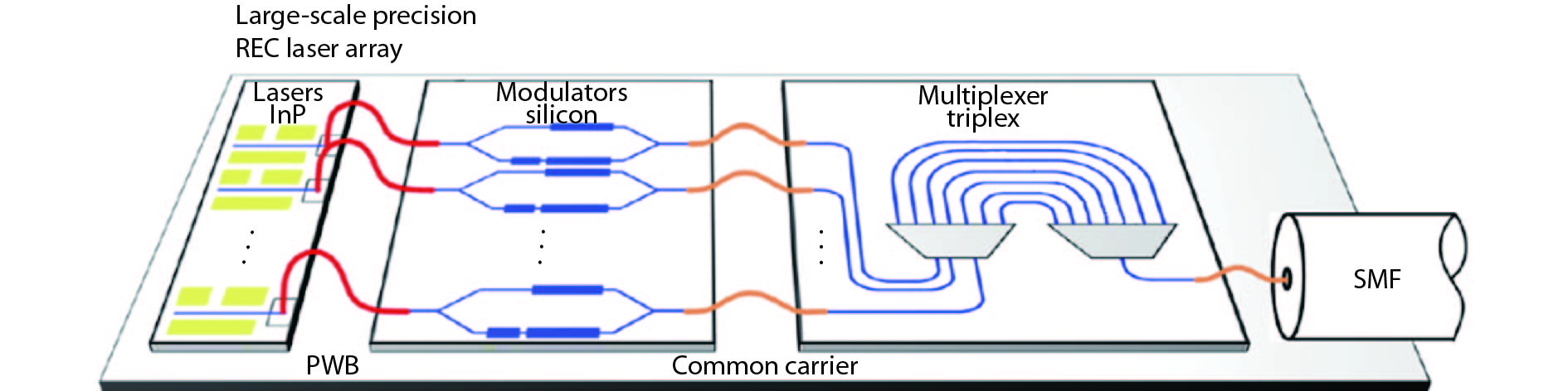
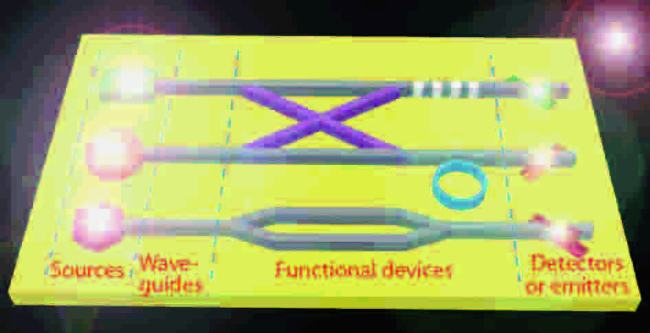
Since the proposal of the concept of photonic integrated circuits (PICs), tremendous progress has been made. In 2005, Infinera Corp. rolled out the first commercial PICs, in which hundreds of optical functions were integrated onto a small form factor chip for wavelength division multiplexing (WDM) systems[
J. Semicond.
2019, 40(5): 052101 doi: 10.1088/1674-4926/40/5/052101

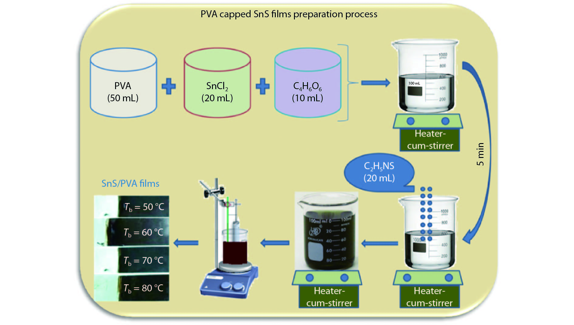
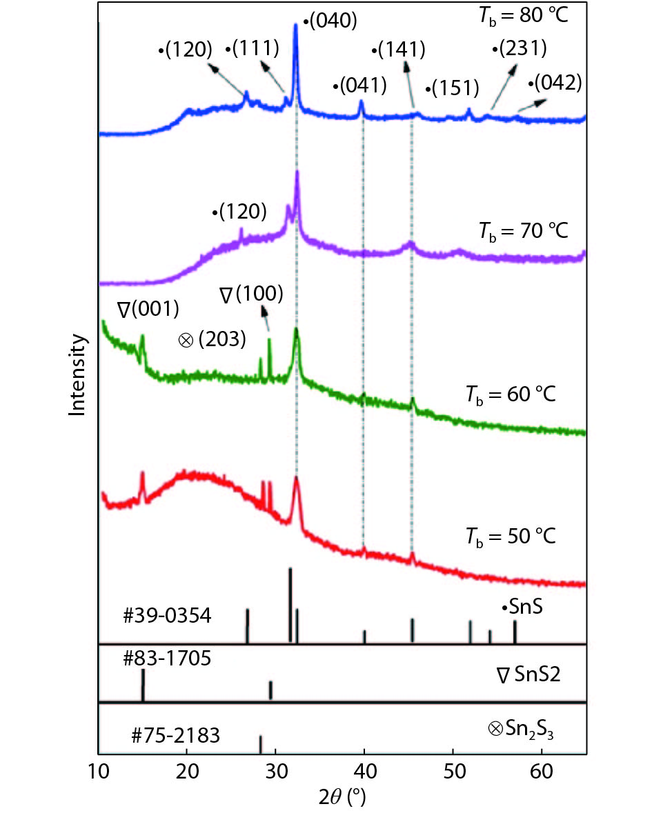
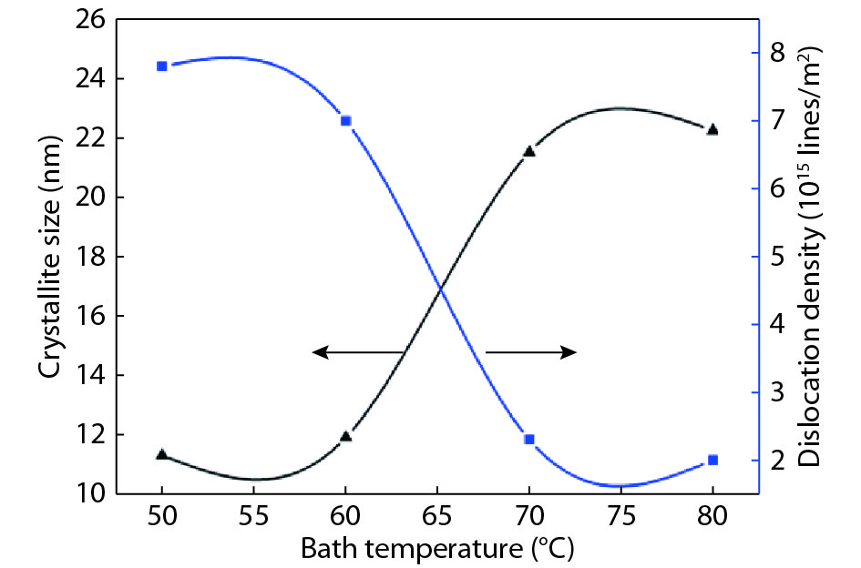
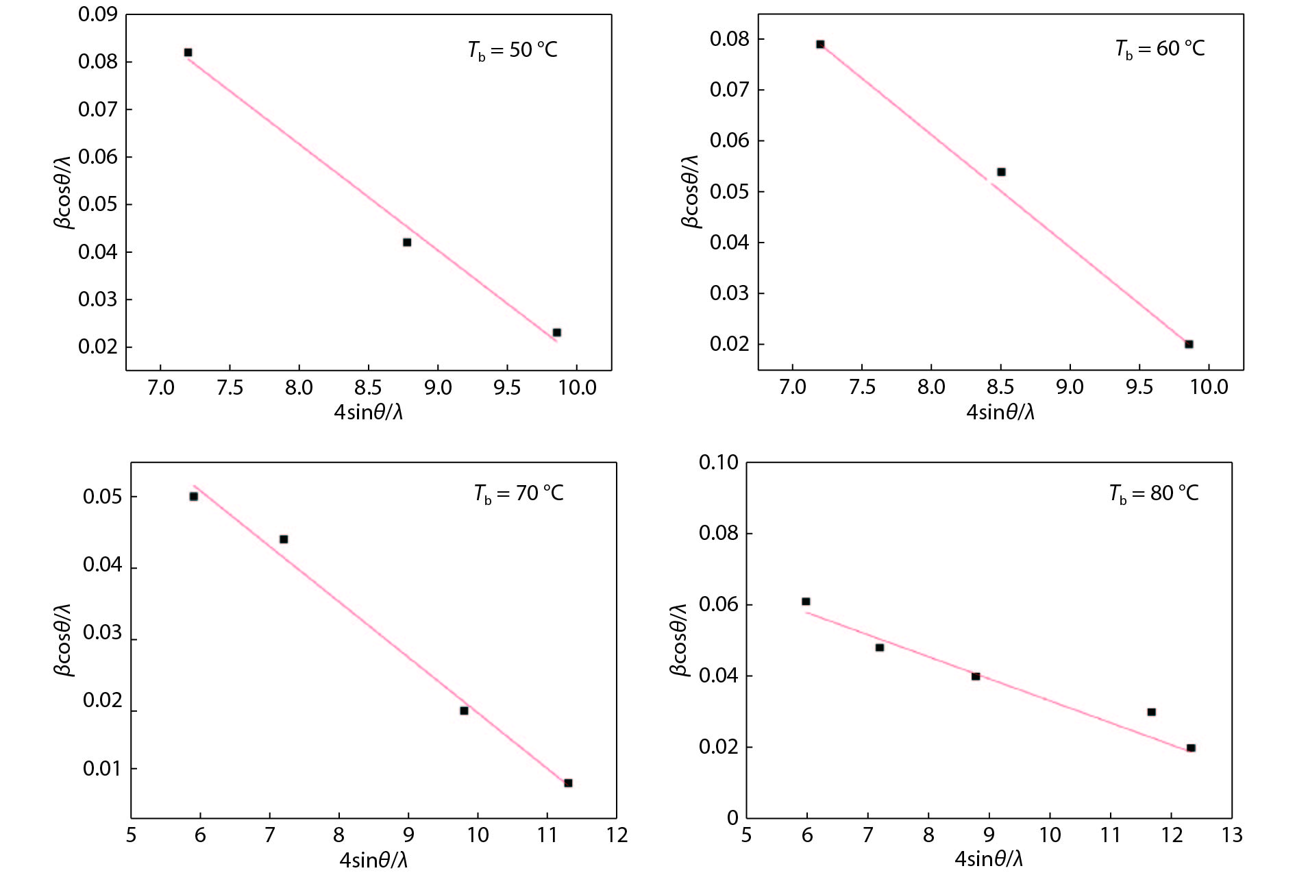
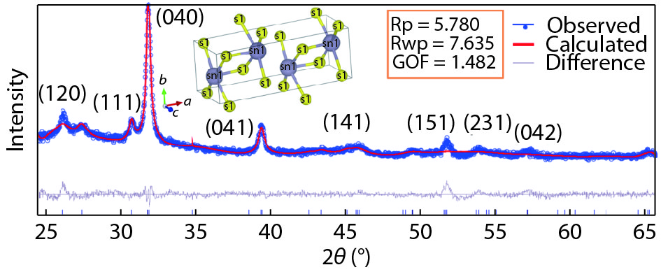
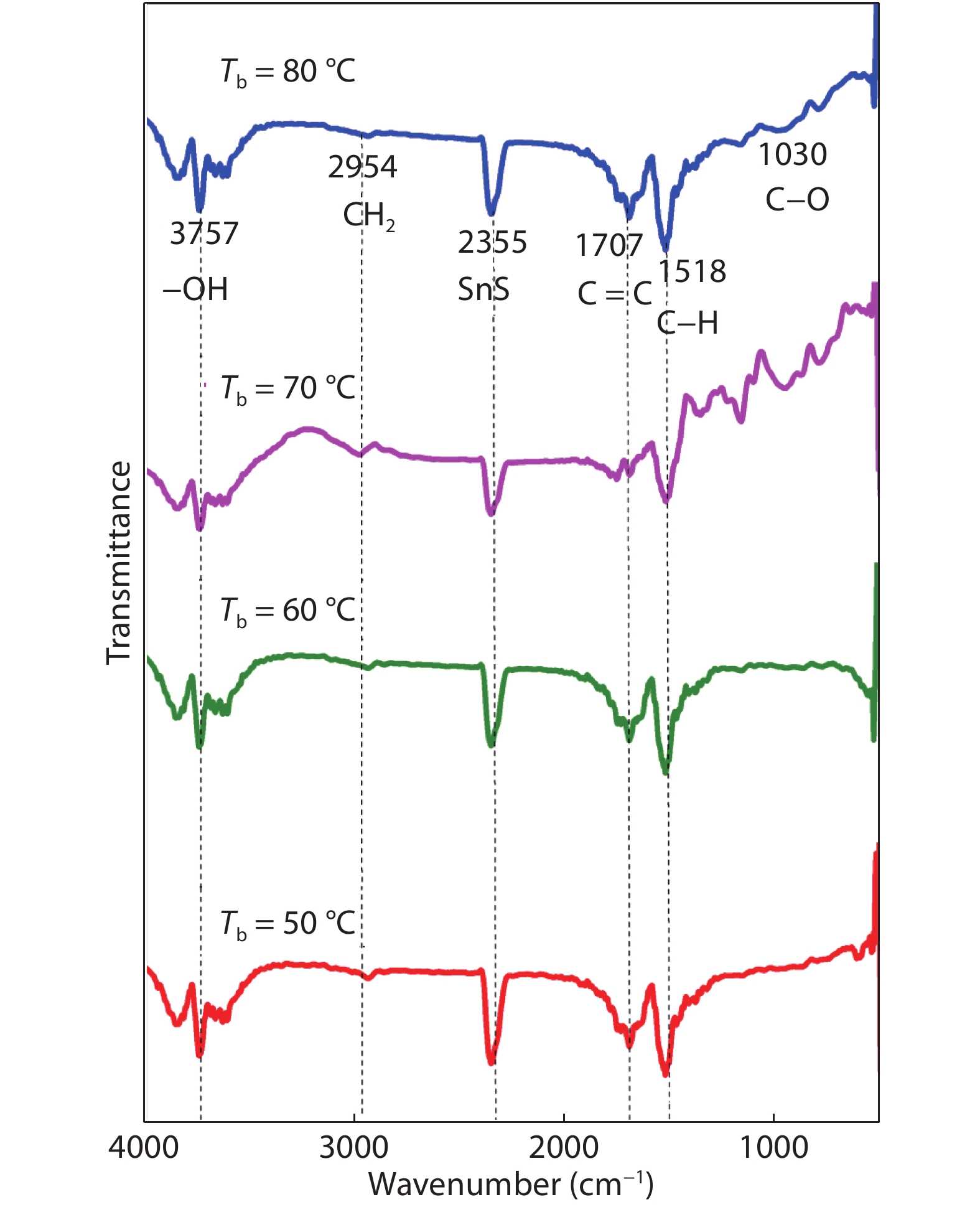
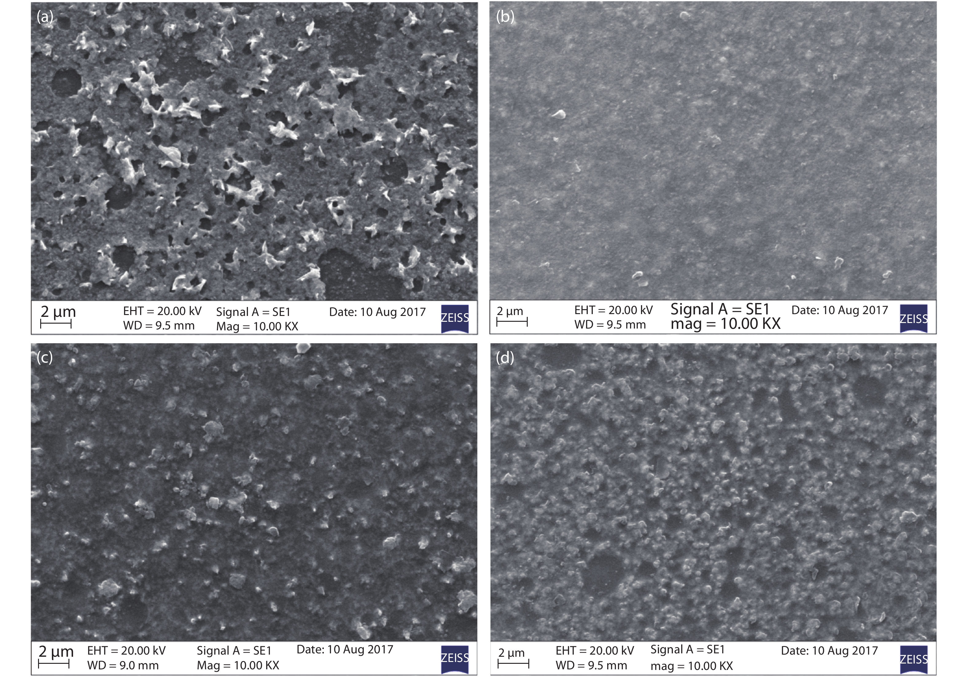
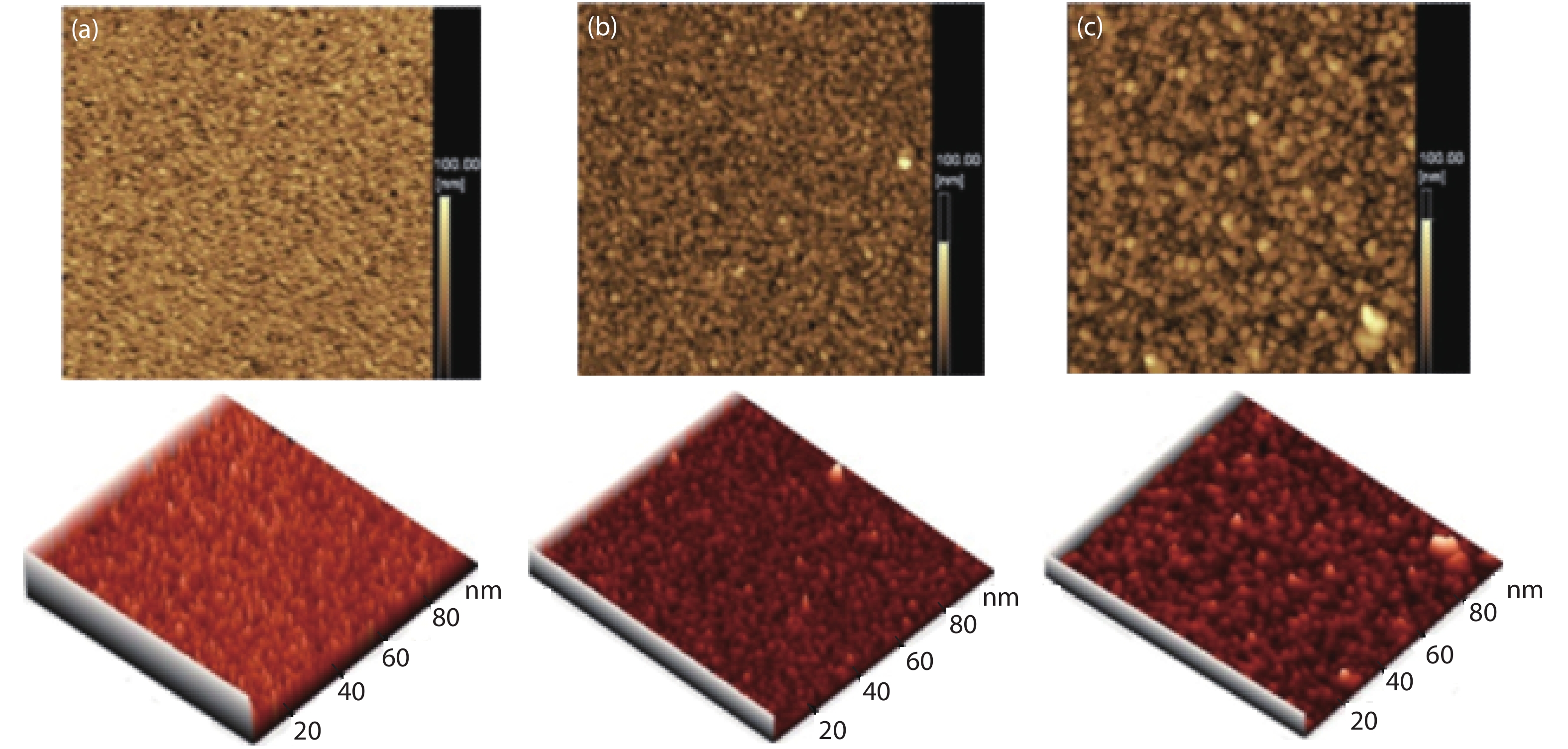
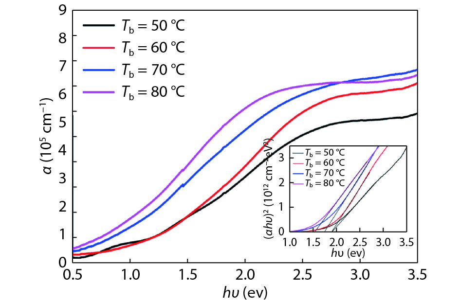
Tin monosulphide (SnS) thin films capped by PVA have been successfully deposited on glass substrates for cost effective photovoltaic device applications by a simple and low-cost wet chemical process, chemical bath deposition (CBD) at different bath temperatures varying in the range, 50–80 °C. X–ray diffraction analysis showed that the deposited films were polycrystalline in nature, showing orthorhombic structure with an intense peak corresponding to (040) plane of SnS. These observations were further confirmed by Raman analysis. FTIR spectra showed the absorption bands which corresponds to PVA in addition to SnS. The scanning electron microscopy and atomic force microscopy studies revealed that the deposited SnS films were uniform and nanostructured with an average particle size of 4.9 to 7.6 nm. The optical investigations showed that the layers were highly absorbing with the optical absorption coefficient ~105 cm–1. A decrease in optical band gap from 1.92 to 1.55 eV with an increase of bath temperature was observed. The observed band gap values were higher than the bulk value of 1.3 eV, which might be due to quantum confinement effect. The optical band gap values were also used to calculate particle size and the results are discussed.


J. Semicond.
2019, 40(5): 052201 doi: 10.1088/1674-4926/40/5/052201
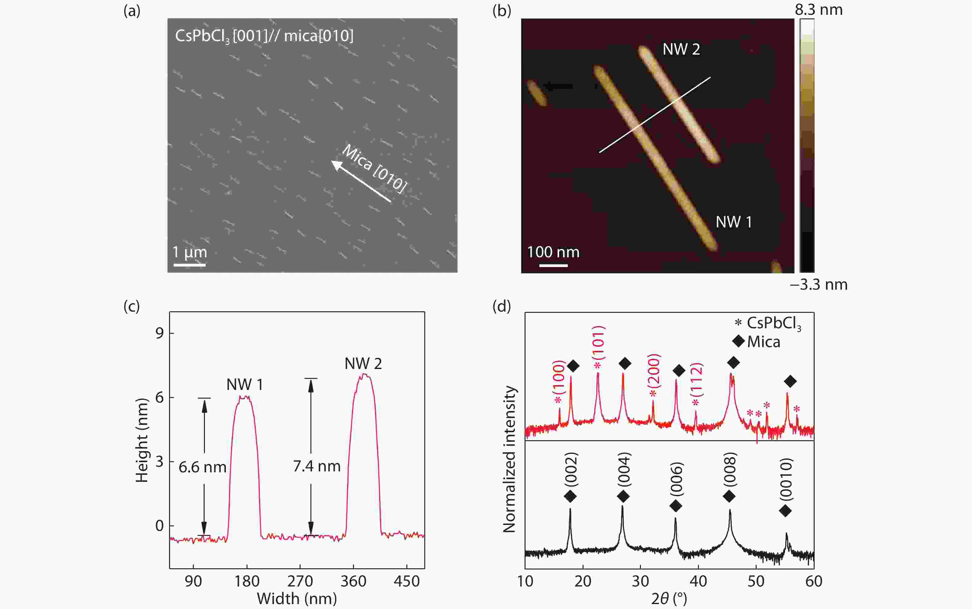
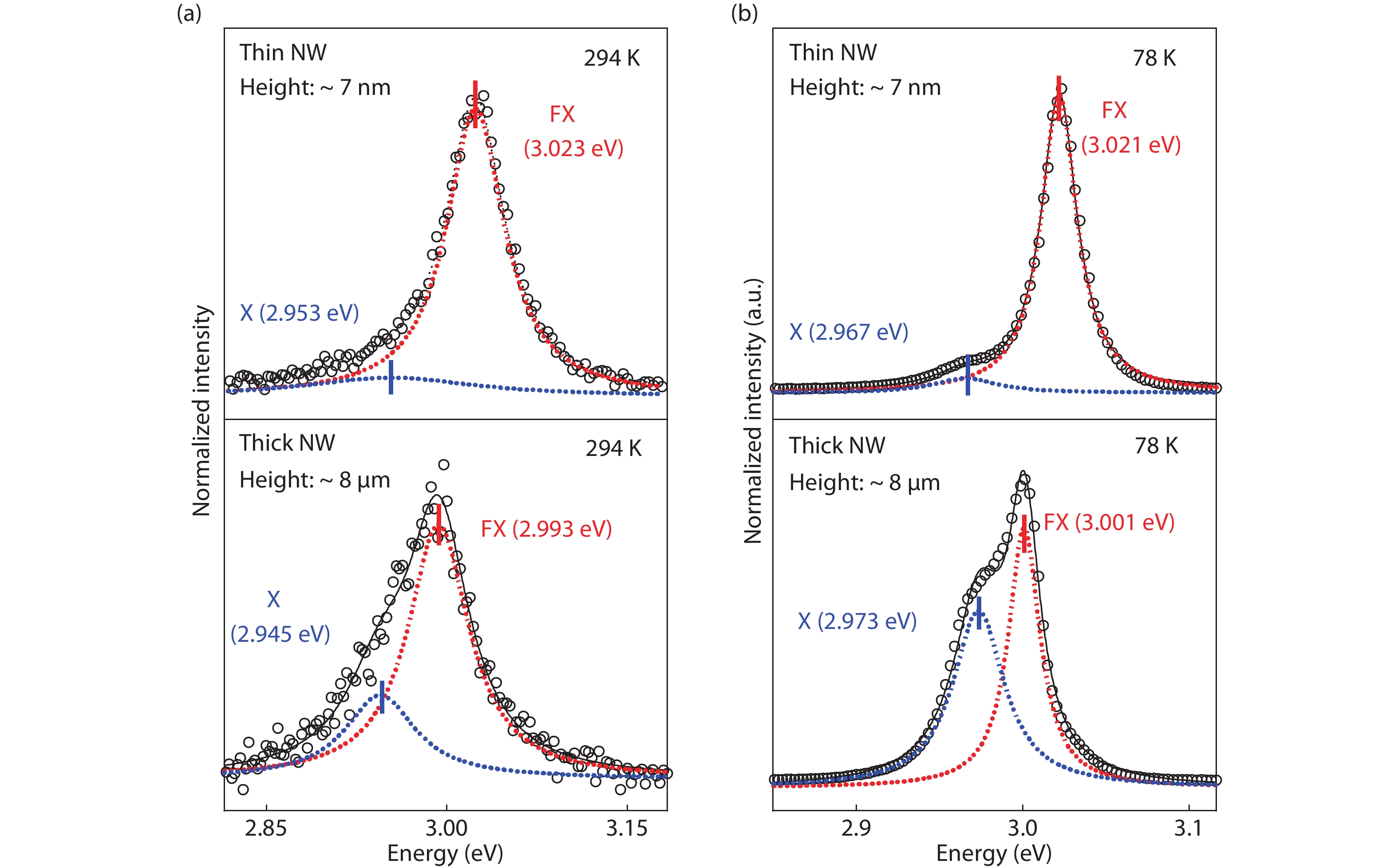
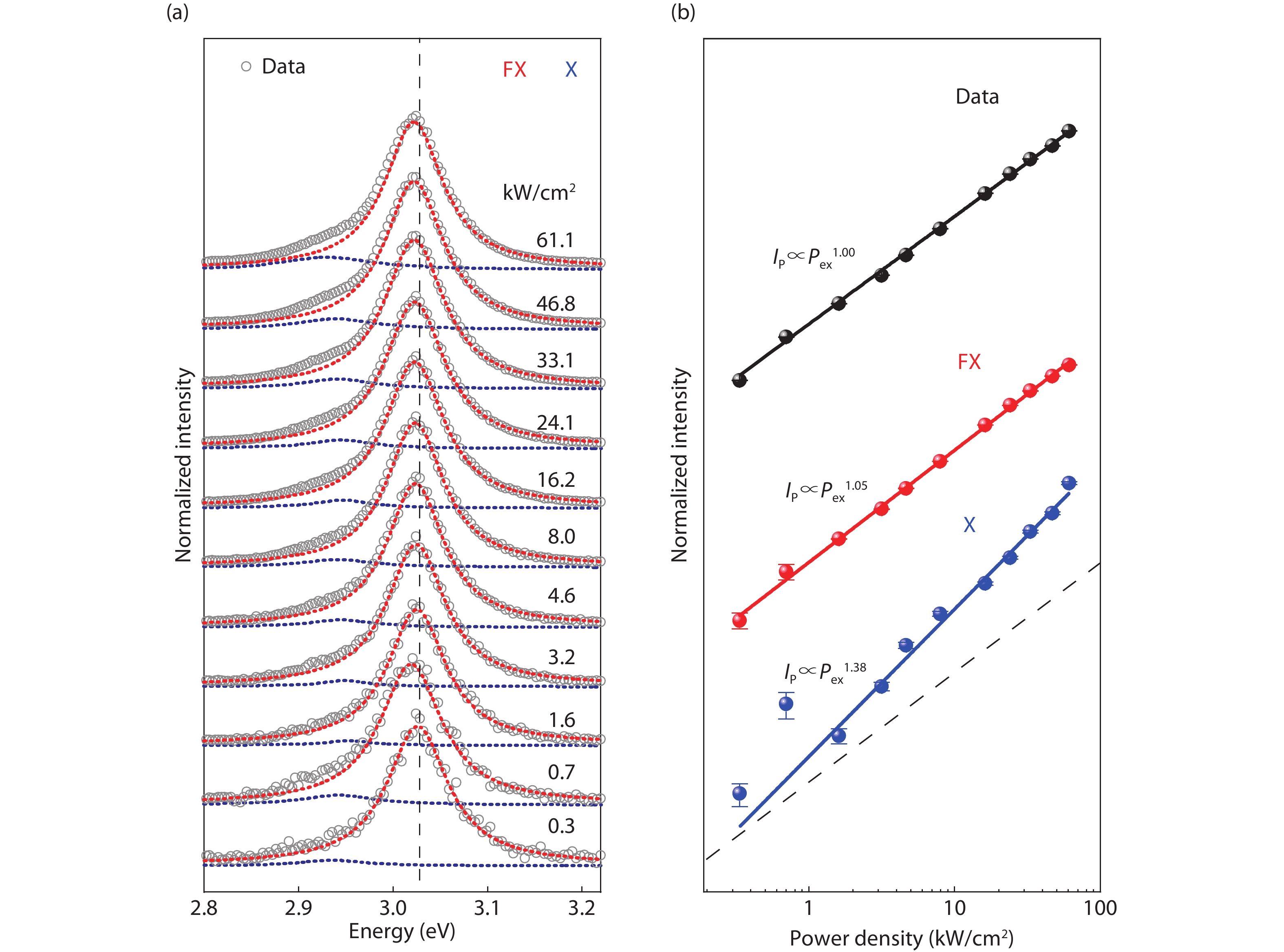
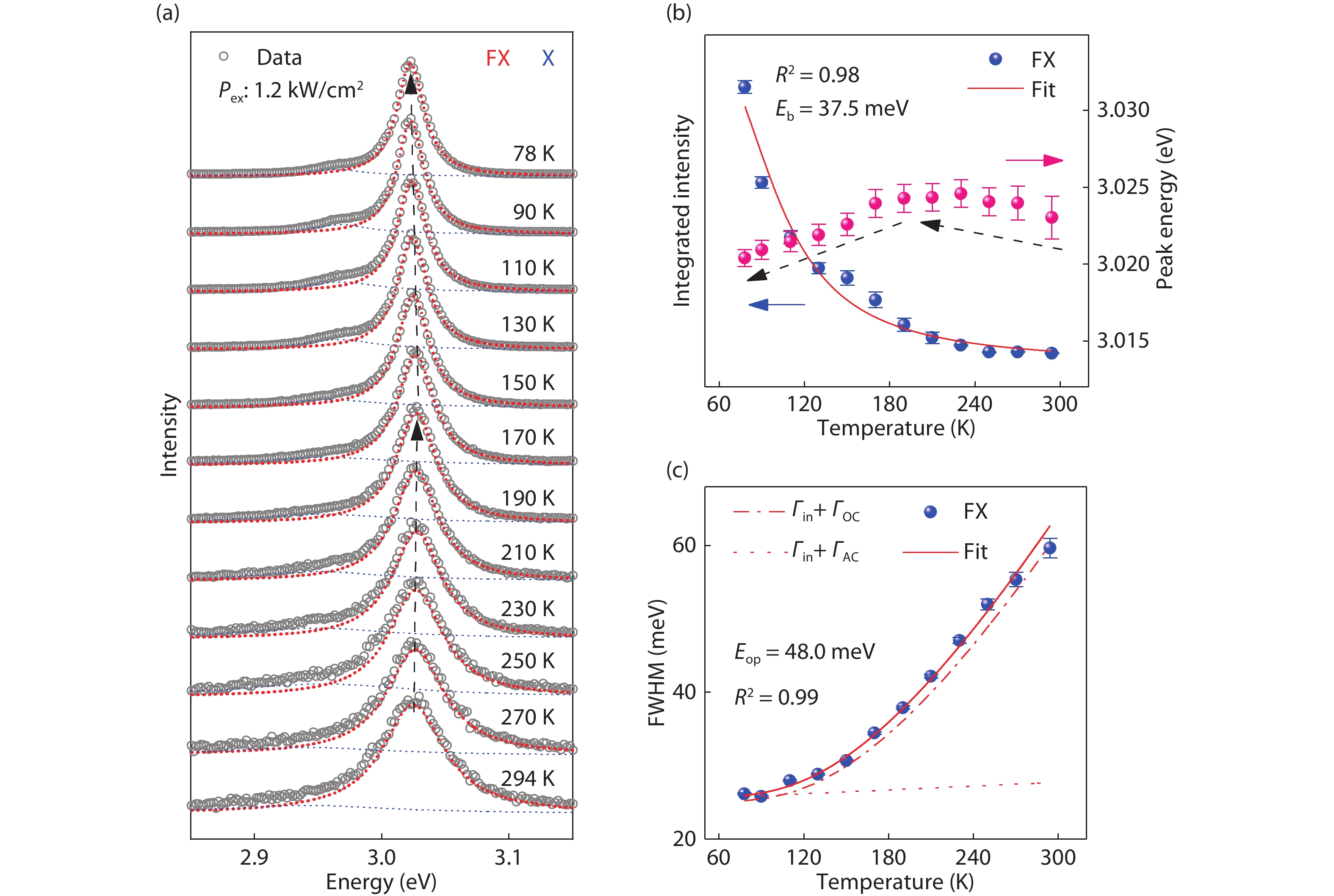
Fabricating high-quality cesium lead chloride (CsPbCl3) perovskite nanowires (NWs) with dimension below 10 nm is not only of interests in fundamental physics, but also holds the great promise for optoelectronic applications. Herein, ultrathin CsPbCl3 NWs with height of ~7 nm, have been achieved via vapor phase deposition method. Power and temperature-dependent photoluminescence (PL) spectroscopy is performed to explore the emission properties of the CsPbCl3 NWs. Strong free exciton recombination is observed at ~3.02 eV as the temperature (T) is 78−294 K with binding energy of ~ 37.5 meV. With the decreasing of T, the PL peaks exhibit a first blueshift by 2 meV for T ~ 294−190 K and then a redshift by 4 meV for T ~ 190−78 K. The exciton–optical phonon interaction plays a major role in the linewidth broadening of the PL spectra with average optical phonon energy of ~48.0 meV and the interaction coefficient of 203.9 meV. These findings advance the fabrication of low dimensional CsPbCl3 perovskite and provide insights into the photophysics of the CsPbCl3 perovskite.
J. Semicond.
2019, 40(5): 052301 doi: 10.1088/1674-4926/40/5/052301
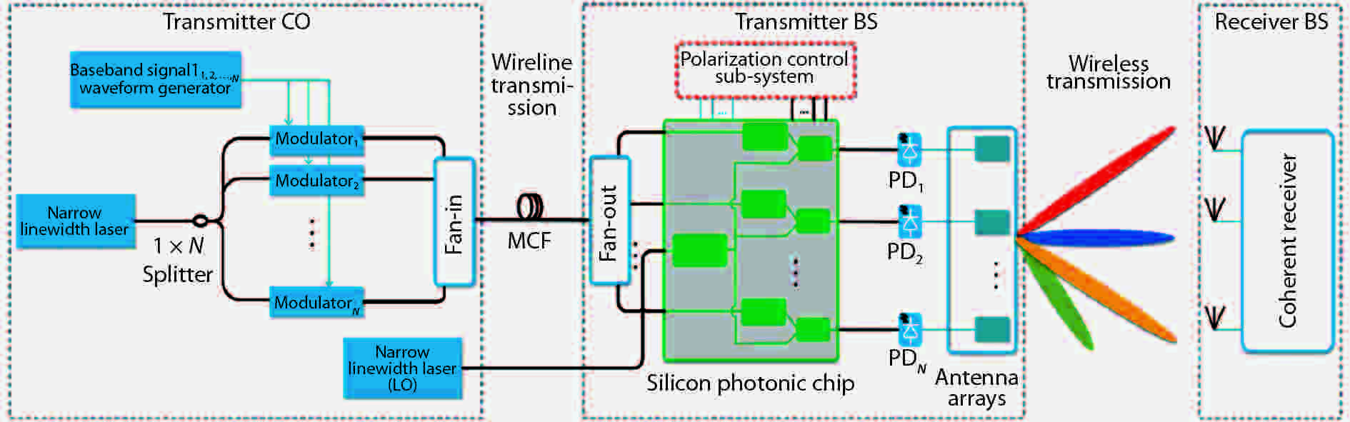
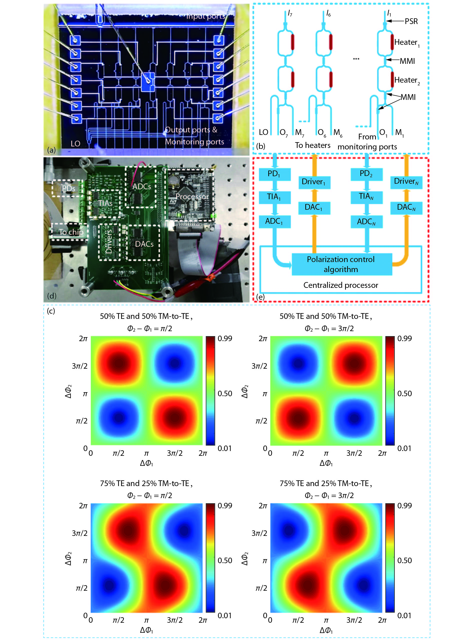
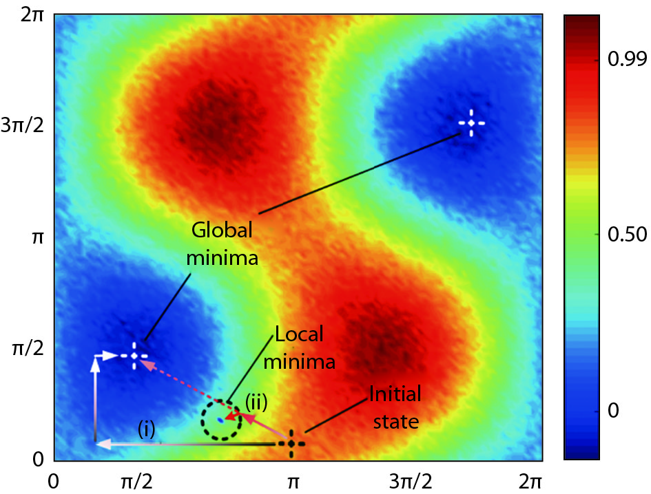
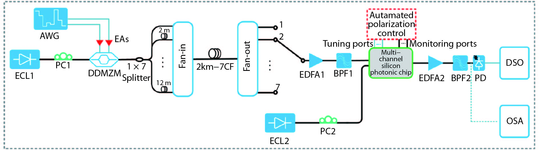
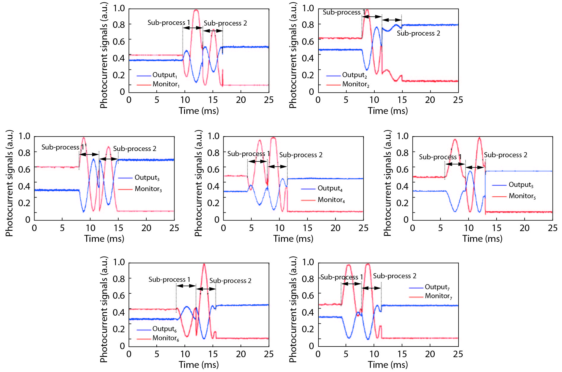
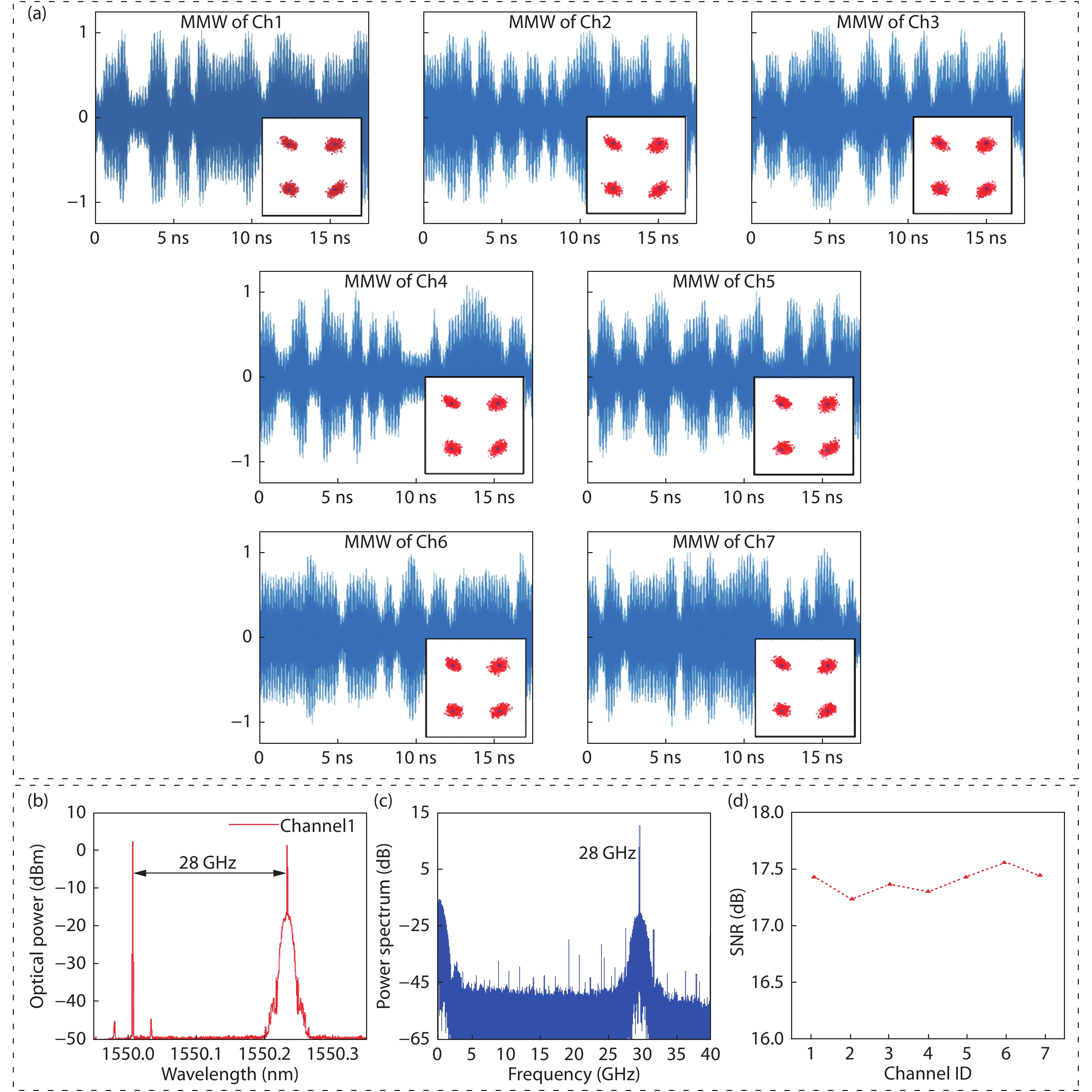
We propose and experimentally demonstrate an integrated silicon photonic scheme to generate multi-channel millimeter-wave (MMW) signals for 5G multi-user applications. The fabricated silicon photonic chip has a footprint of 1.1 × 2.1 mm2 and integrates 7 independent channels each having on-chip polarization control and heterodyne mixing functions. 7 channels of 4-Gb/s QPSK baseband signals are delivered via a 2-km multi-core fiber (MCF) and coupled into the chip with a local oscillator (LO) light. The polarization state of each signal light is automatically adjusted and aligned with that of the LO light, and then 7 channels of 28-GHz MMW carrying 4-Gb/s QPSK signals are generated by optical heterodyne beating. Automated polarization-control function of each channel is also demonstrated with ~7-ms tuning time and ~27-dB extinction ratio.


J. Semicond.
2019, 40(5): 052401 doi: 10.1088/1674-4926/40/5/052401

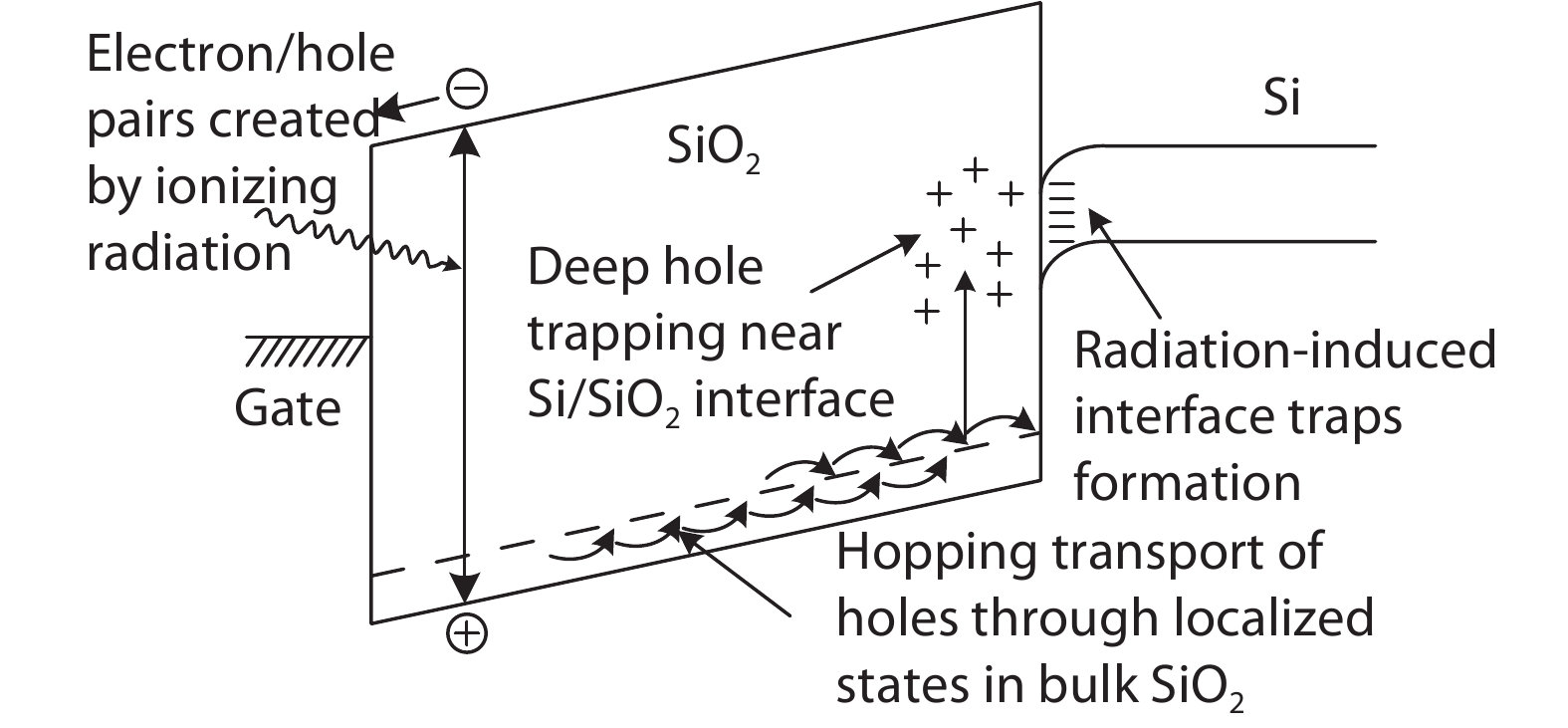
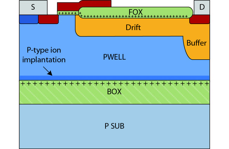
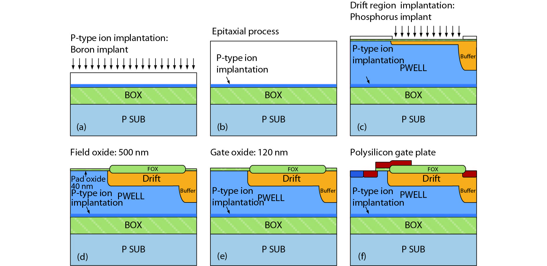
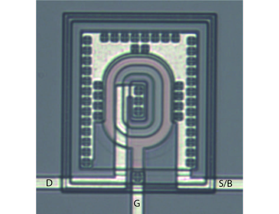
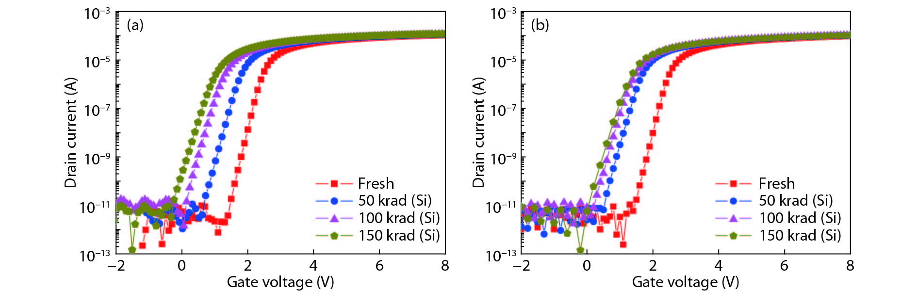
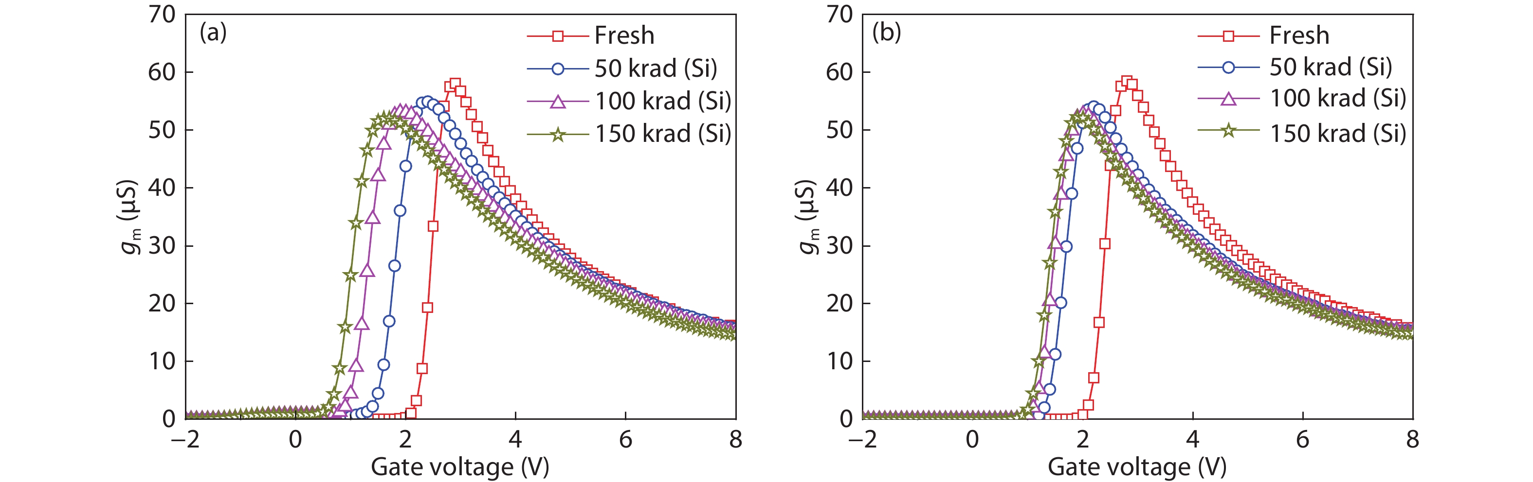
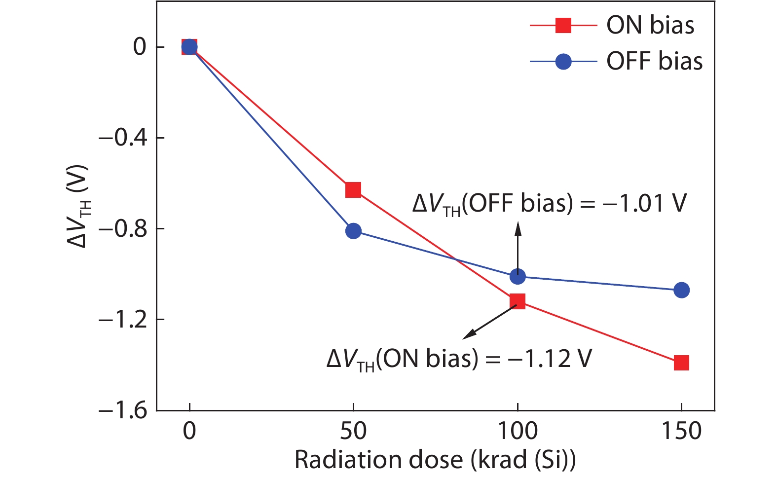
Based on the silicon-on-insulator (SOI) technology and radiation-hardened silicon gate (RSG) process, a radiation-hardened high-voltage lateral double-diffused MOSFET (LDMOS) device is presented in this paper. With the gate supply voltage of 30 V, the LDMOS device has a gate oxide thickness of 120 nm, and the RSG process is effective in reducing the total ionizing dose (TID) radiation-induced threshold voltage shift. The p-type ion implantation process and gate-enclosed layout topology are used to prevent radiation-induced leakage current through a parasitic path under the bird's beak and at the deep trench corner, and the device is compatible with high-voltage SOI CMOS process. In the proposed LDMOS, the total ionizing dose radiation degradation for the ON bias is more sensitive than the OFF bias. The experiment results show that the SOI LDMOS has a negative threshold voltage shift of 1.12 V, breakdown voltage of 135 V, and off-state leakage current of 0.92 pA/μm at an accumulated dose level of 100 krad (Si).


J. Semicond.
2019, 40(5): 052402 doi: 10.1088/1674-4926/40/5/052402
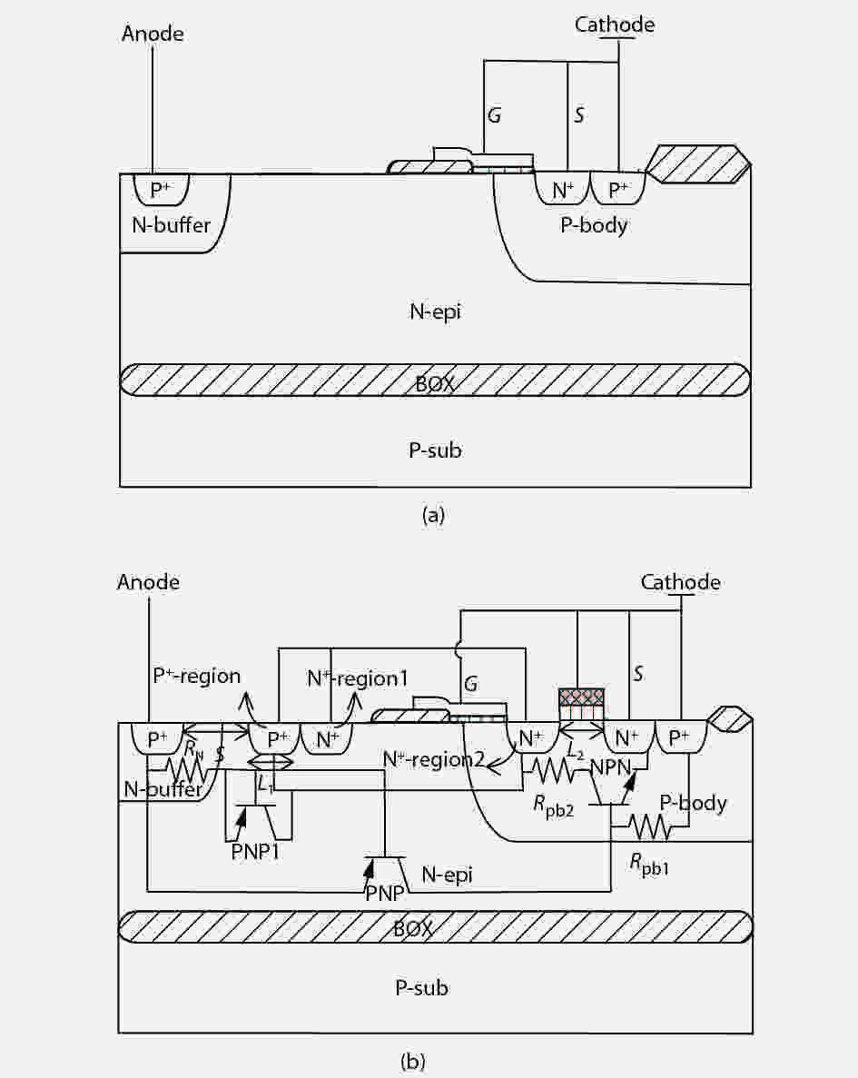
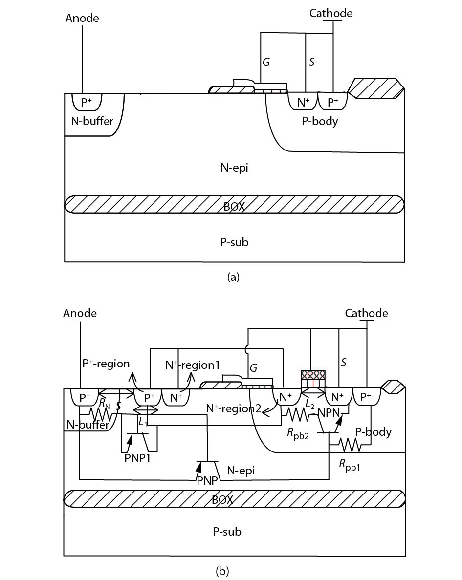
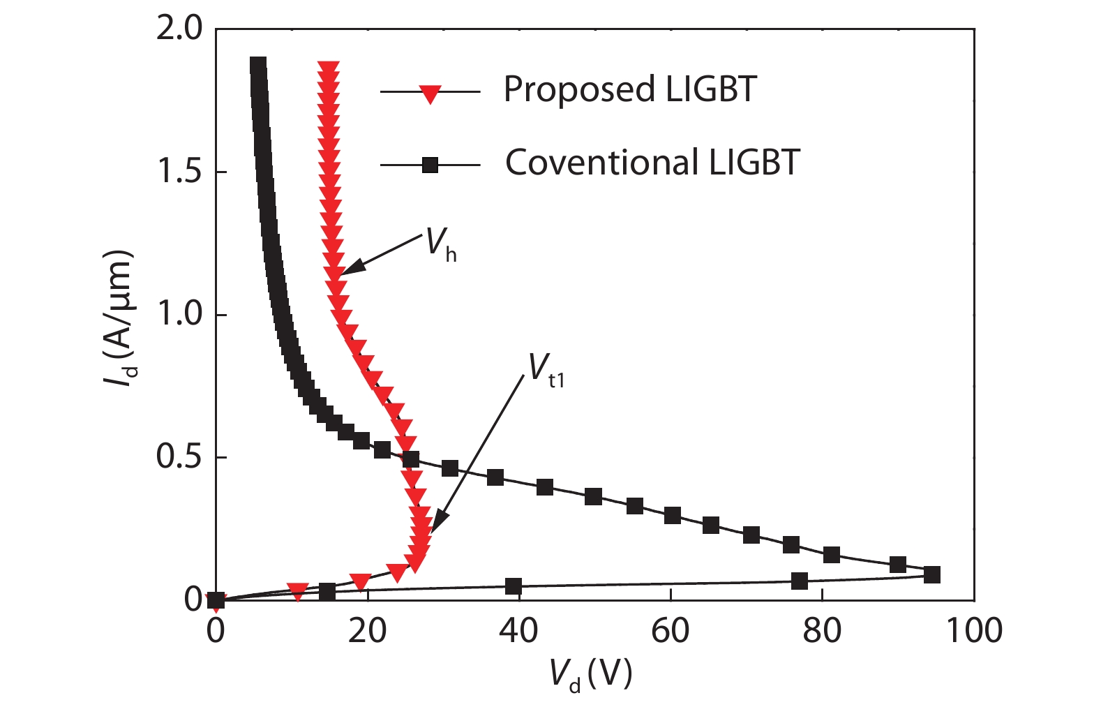
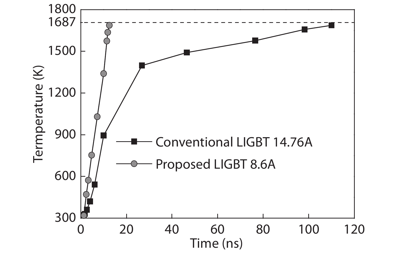
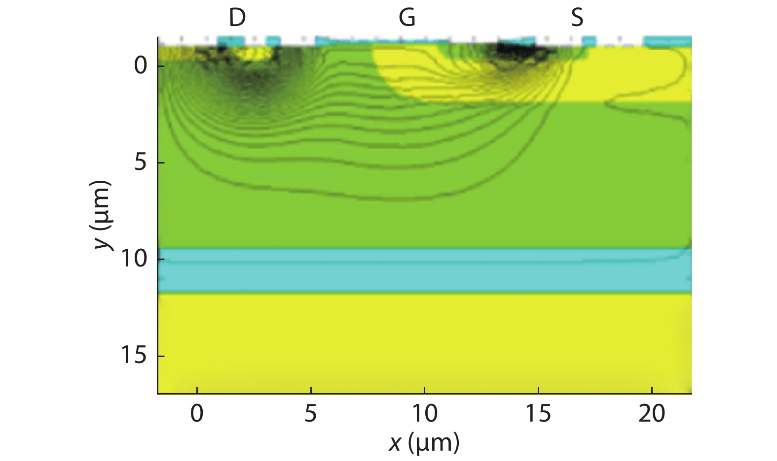
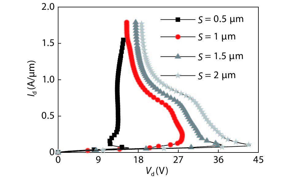
A novel NMOS triggered LIGBT (NTLIGBT) structure is proposed for electrostatic discharge (ESD) protection in this paper. The structure utilizes internal NMOS to trigger SCR-like structure in LIGBT. The trigger voltage is significantly reduced because the embedded NMOS causes N+-drain/P-body junction being apt to avalanche breakdown. At the same time, the new parasitic PNP transistor including the newly added P+-region as a collector forms another path to bleed ESD current and then the conductivity modulation in the LIGBT is weakened. As a result, the holding voltage is increased. So, the proposed NTLIGBT structure has a narrow ESD design window. The simulation results show an improvement of 71.5% in trigger voltage and over 50% in holding voltage comparing with the conventional LIGBT structure.


J. Semicond.
2019, 40(5): 052501 doi: 10.1088/1674-4926/40/5/052501
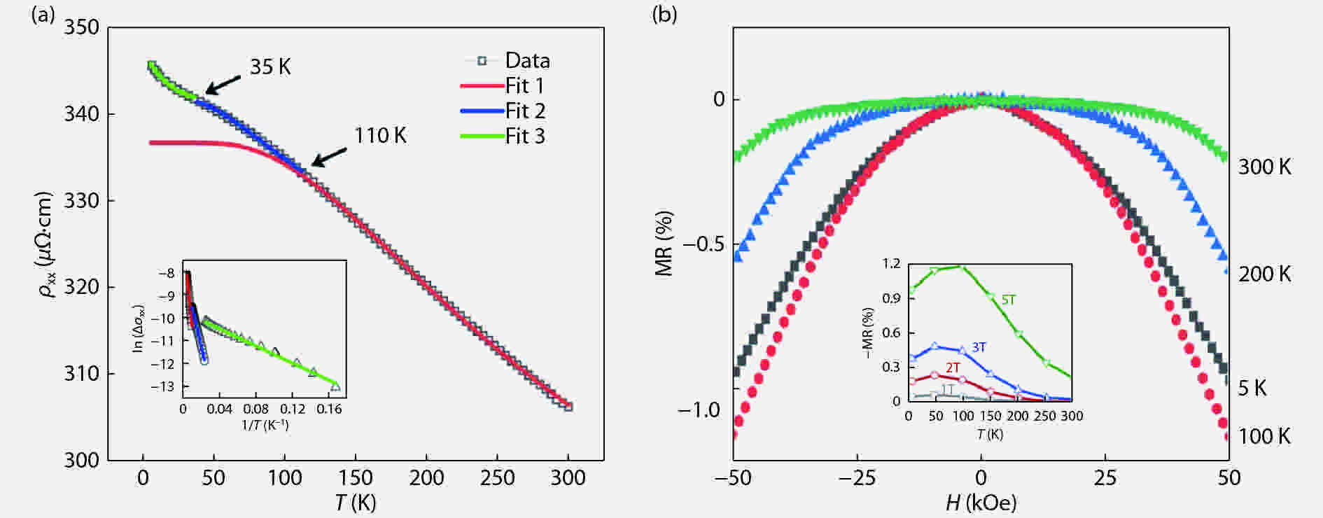
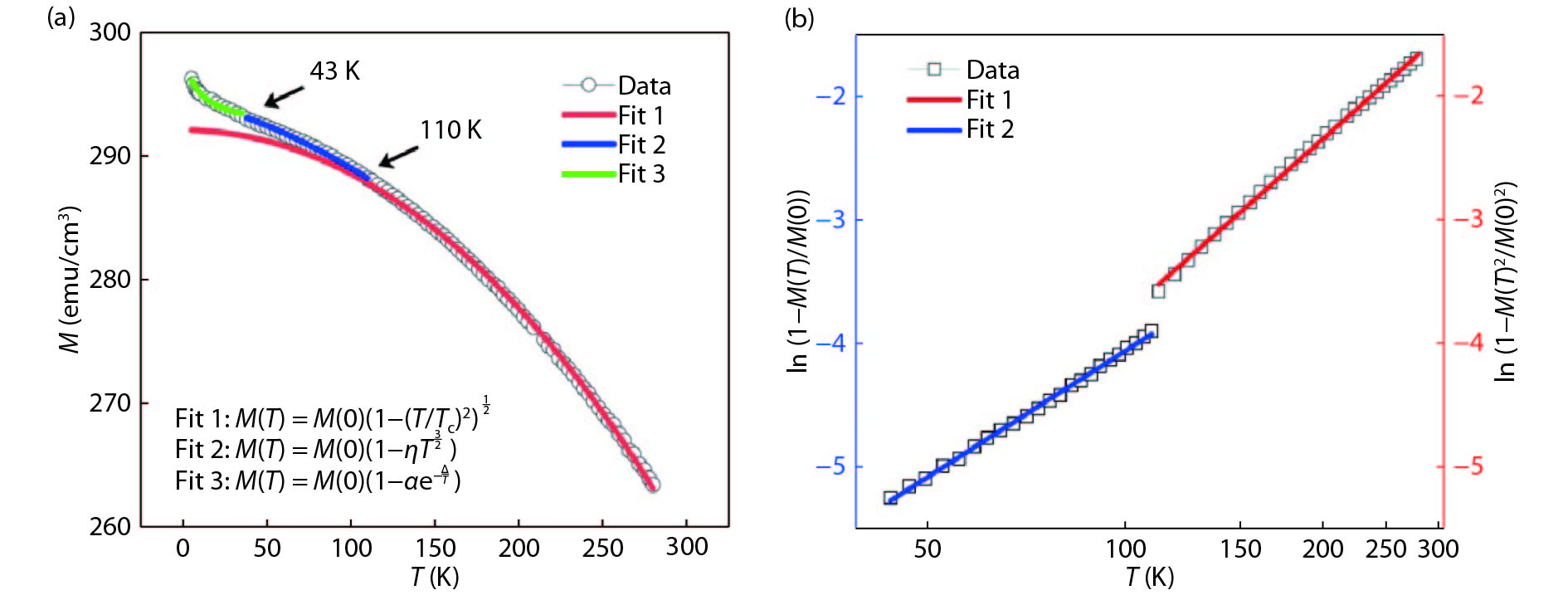
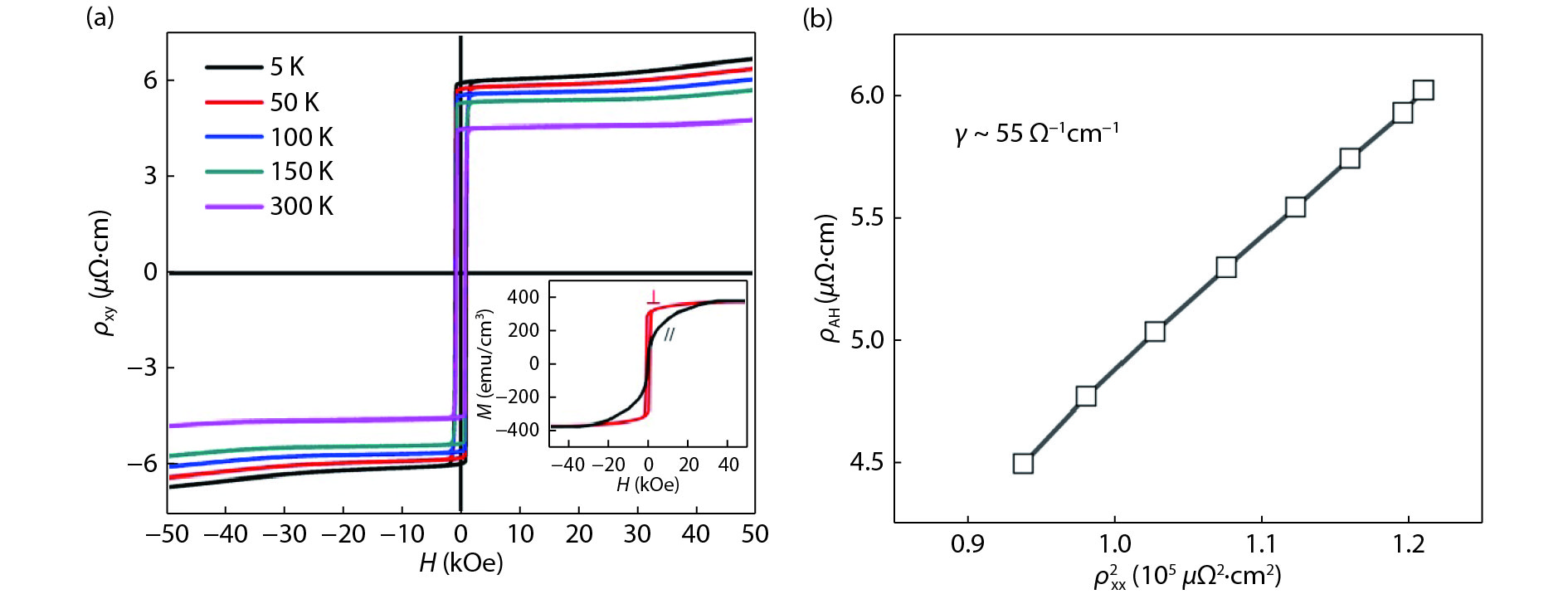
We have investigated the magneto-transport properties of an off-stoichiometric full-Heusler alloy Co2MnAl single-crystalline film. The Co1.65Mn1.35Al (CMA) film epitaxially grown on Ⅲ–Ⅴ semiconductor GaAs substrate exhibits perpendicular magnetic anisotropy. The resistivity of the CMA film increases with the temperature T decreasing from 300 to 5 K, showing a semiconducting-like transport behavior. Different activation energies are found in three temperature regions with transition temperatures of 35 and 110 K. In the meanwhile, the remanent magnetization can be described by T3/2 and T2 laws in the corresponding medium and high T ranges, respectively. The transition at around 110 K could be attributed to the ferromagnetism evolving from localized to itinerant state. The Curie temperature of the CMA film is estimated to be ~640 K. The intrinsic anomalous Hall conductivity of ~55 Ω–1cm–1 is obtained, which is almost twenty times smaller than that of Co2MnAl.

J. Semicond.
2019, 40(5): 052701 doi: 10.1088/1674-4926/40/5/052701

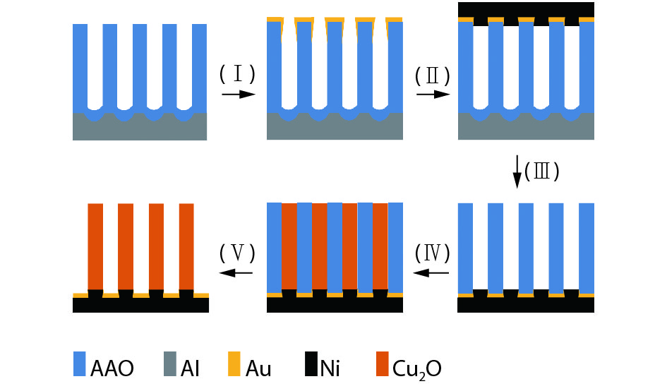
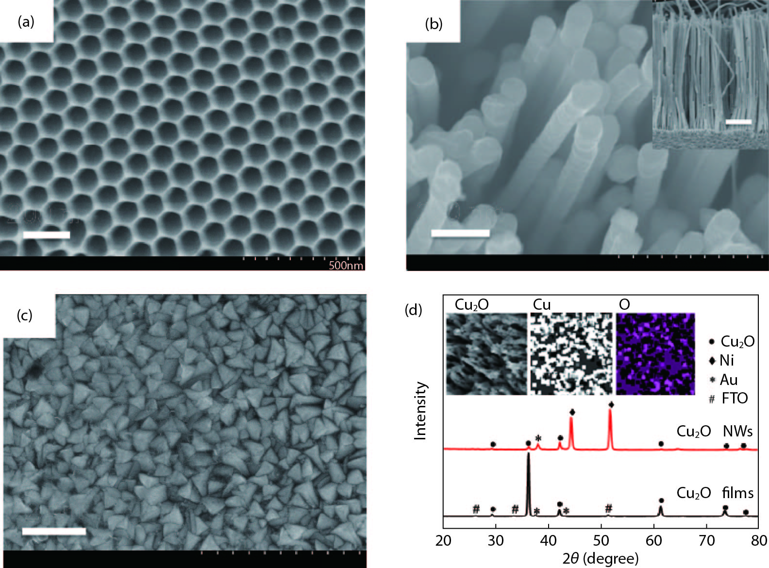
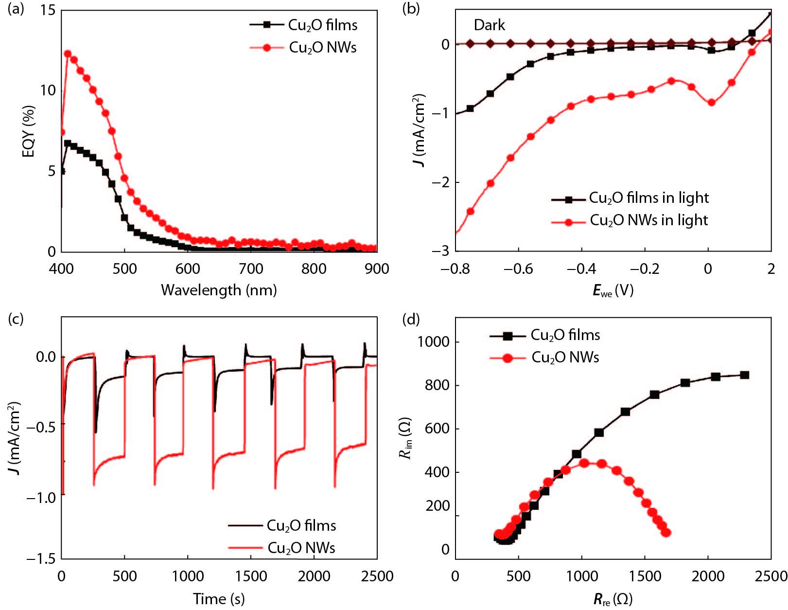
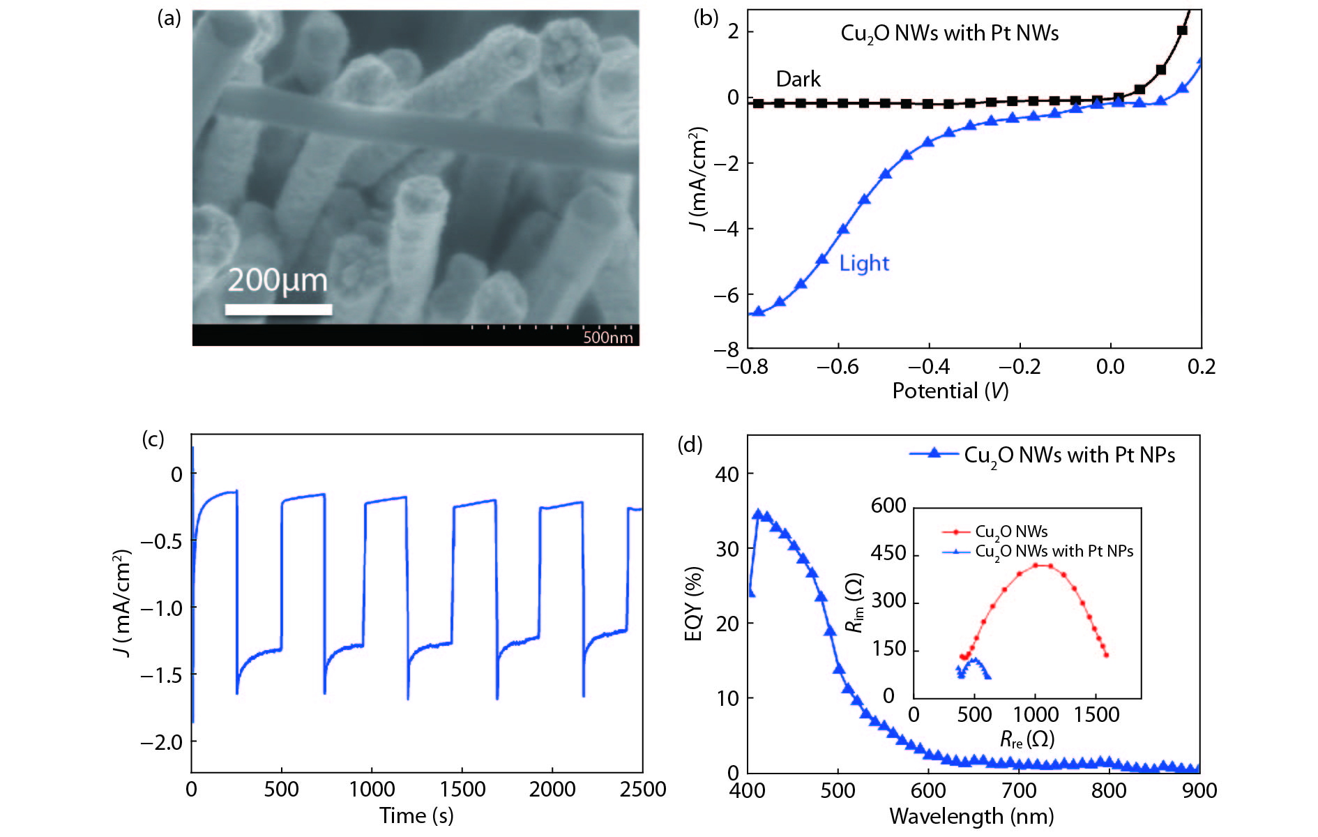
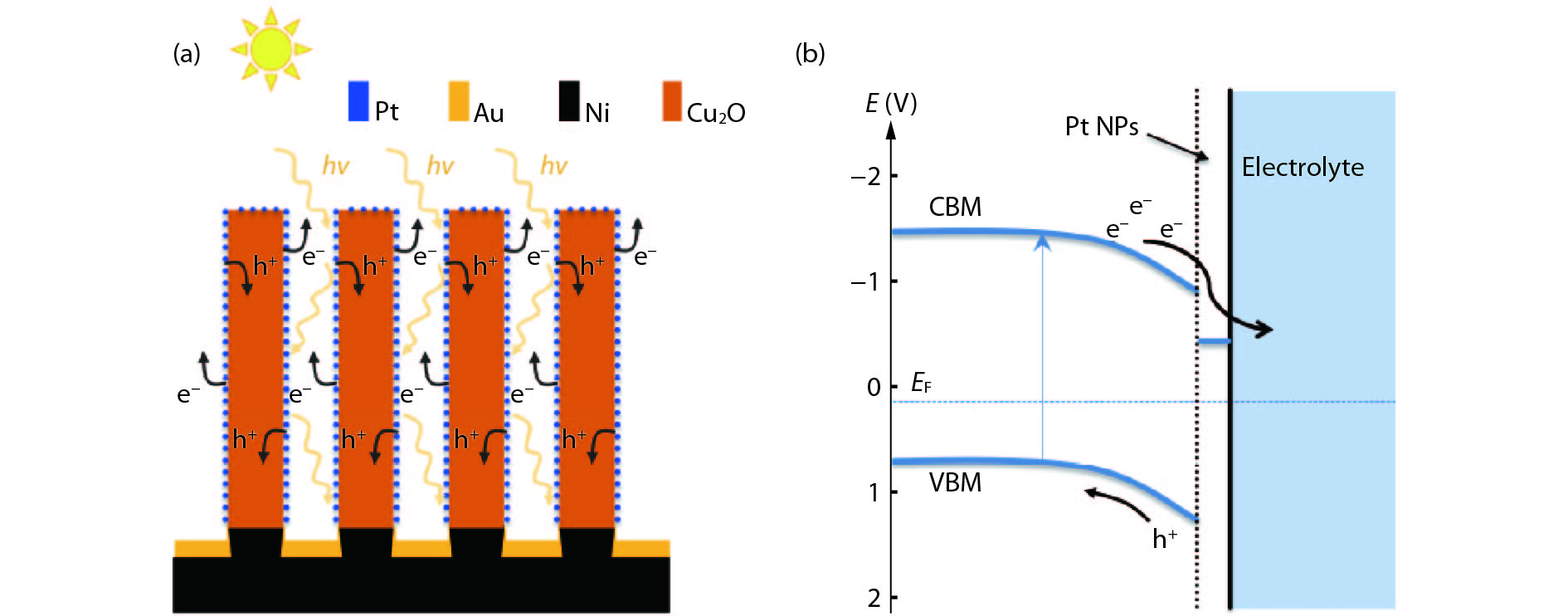
Nanowire (NW) structures is an alternative candidate for constructing the next generation photoelectrochemical water splitting system, due to the outstanding optical and electrical properties. NW photoelectrodes comparing to traditional semiconductor photoelectrodes shows the comparatively shorter transfer distance of photo-induced carriers and the increase amount of the surface reaction sites, which is beneficial for lowering the recombination probability of charge carriers and improving their photoelectrochemical (PEC) performances. Here, we demonstrate for the first time that super-long Cu2O NWs, more than 4.5 μm, with highly efficient water splitting performance, were synthesized using a cost-effective anodic alumina oxide (AAO) template method. In comparison with the photocathode with planar Cu2O films, the photocathode with Cu2O NWs demonstrates a significant enhancement in photocurrent, from –1.00 to –2.75 mA/cm2 at –0.8 V versus Ag/AgCl. After optimization of the photoelectrochemical electrode through depositing Pt NPs with atomic layer deposition (ALD) technology on the Cu2O NWs, the plateau of photocurrent has been enlarged to –7 mA/cm2 with the external quantum yield up to 34% at 410 nm. This study suggests that the photoelectrode based on Cu2O NWs is a hopeful system for establishing high-efficiency water splitting system under visible light.
J. Semicond.
2019, 40(5): 052801 doi: 10.1088/1674-4926/40/5/052801

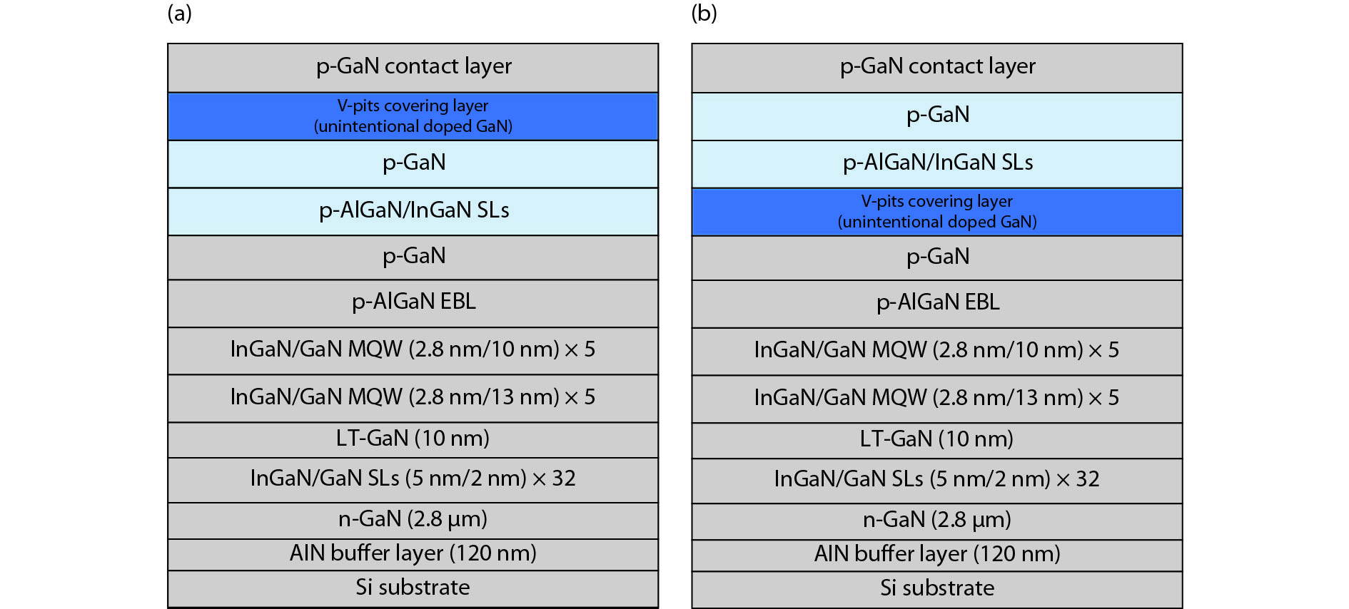
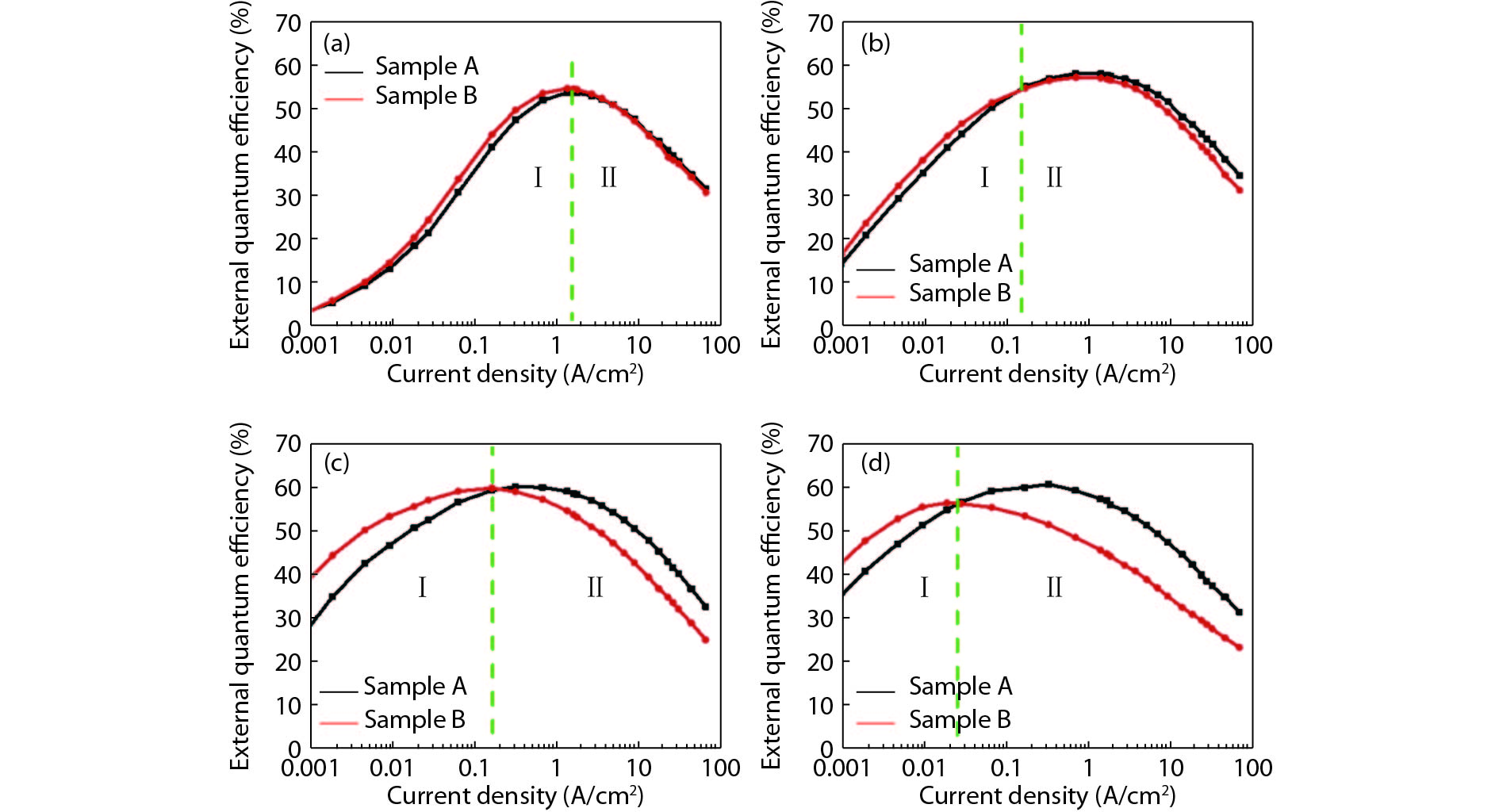
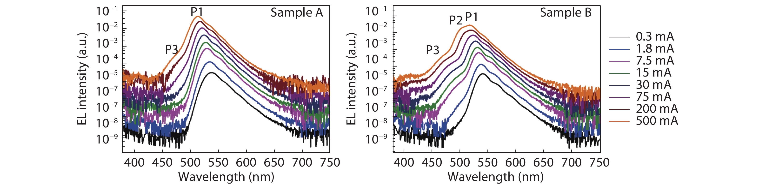
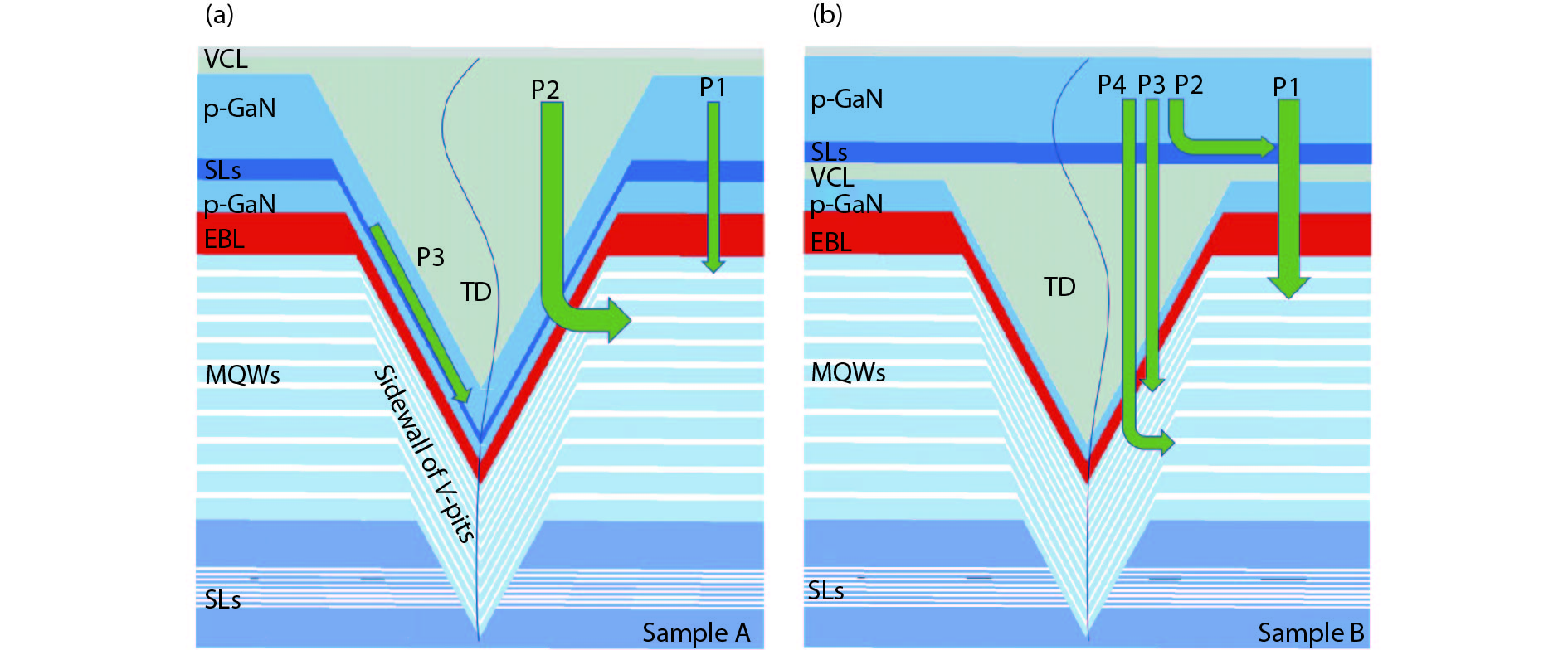
The impact of the V-pits covering layer (VCL) position on the optoelectronic performance of InGaN-based green light-emitting diodes (LEDs) was investigated. It is found that earlier covering of V-pits will hinder the hole injection via the sidewall of V-pits, and then result in less quantum wells (QWs) participating in radioluminescence. The current-voltage characteristics show that the LEDs with earlier covering of V-pits have higher operating voltage at room temperature, and a more dramatic voltage rise with the reduction of temperature. Meanwhile, more manifested emission peaks for sidewall QWs and deeper QWs near to n-type layer was observed in the sample with earlier coveing of V-pits at cryogenic temperatures, for the reason that the holes being injected via V-pits sidewall have higher kinetic energy and could transport to deeper QWs.


J. Semicond.
2019, 40(5): 052802 doi: 10.1088/1674-4926/40/5/052802
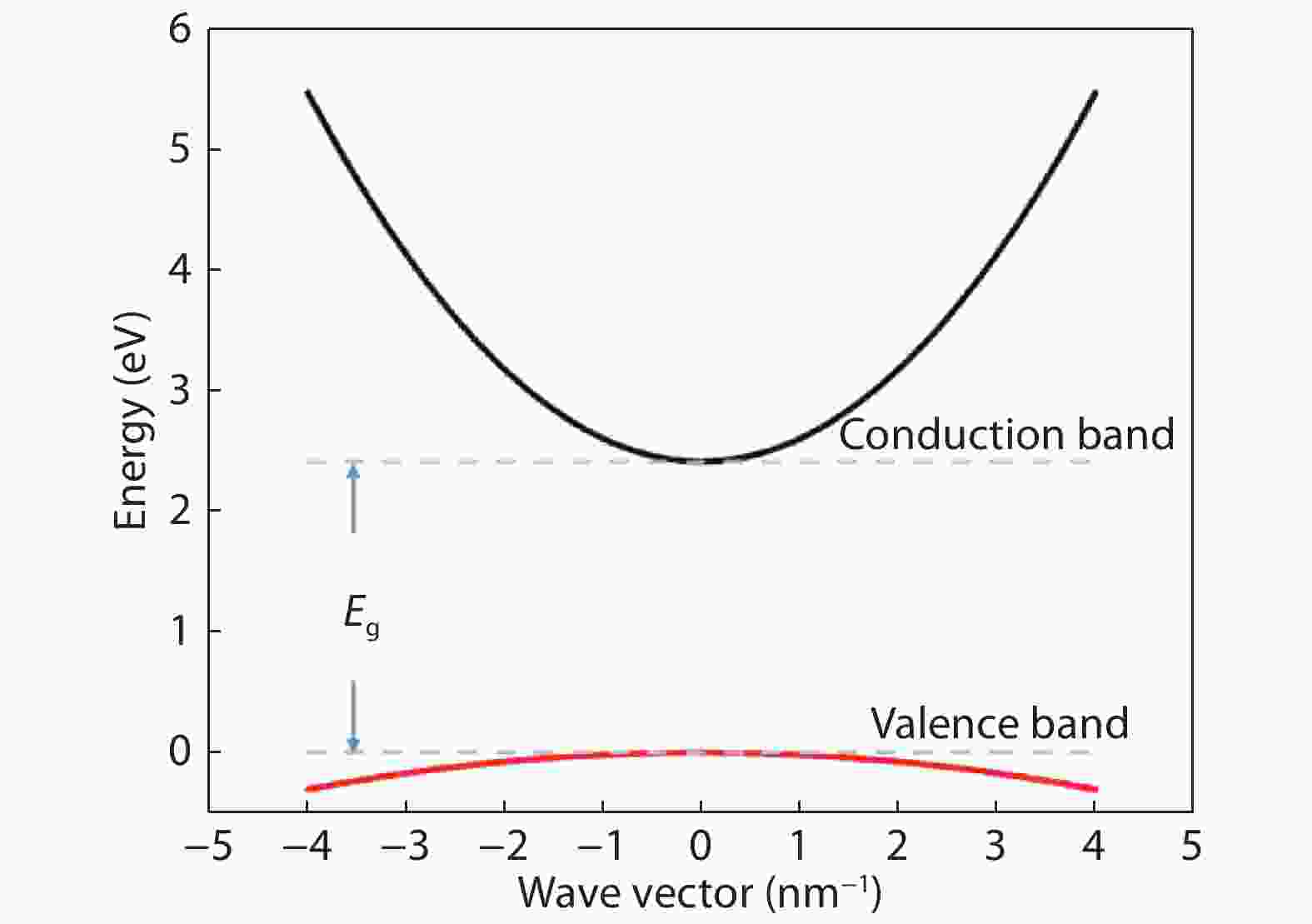
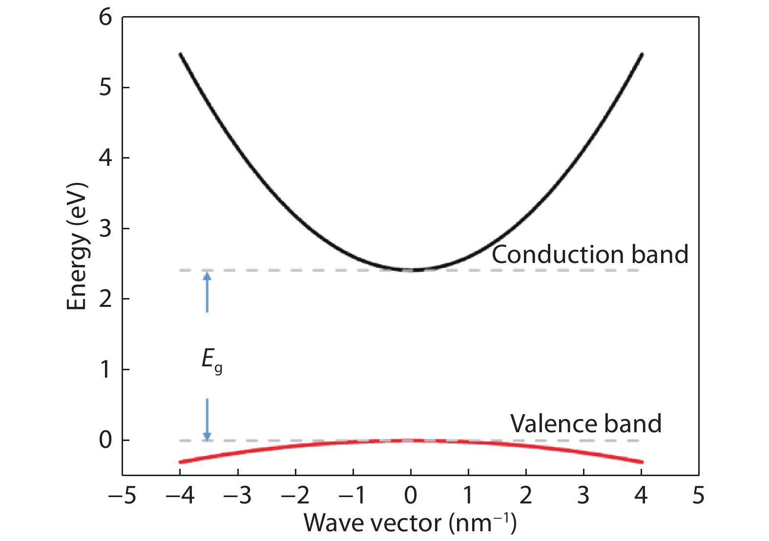
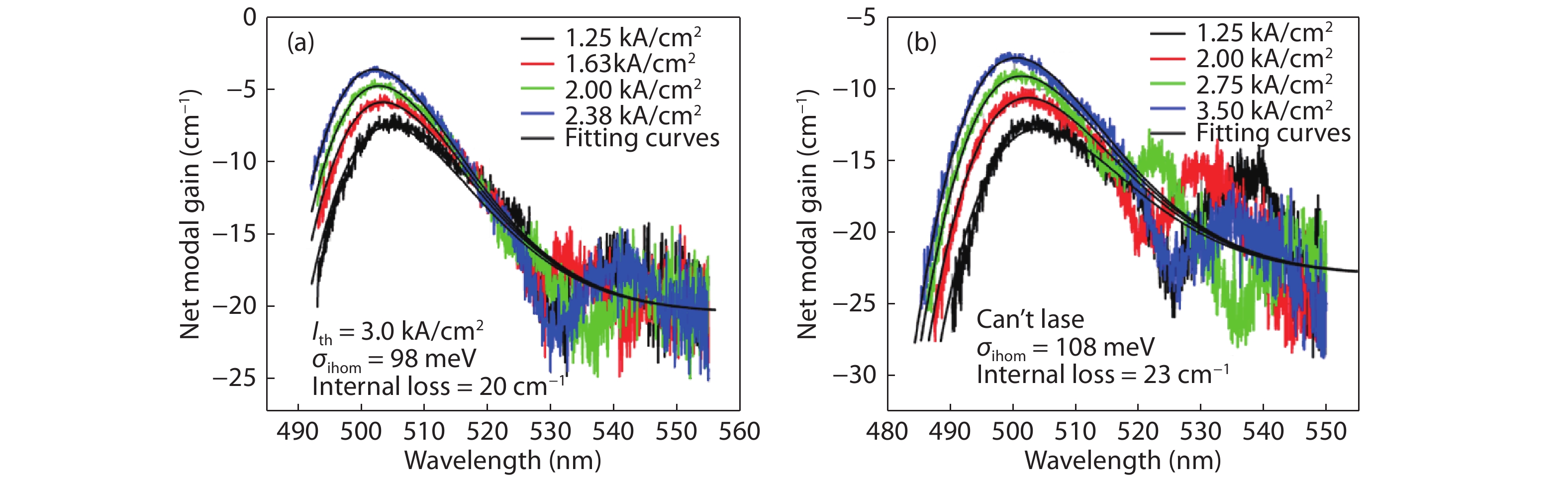
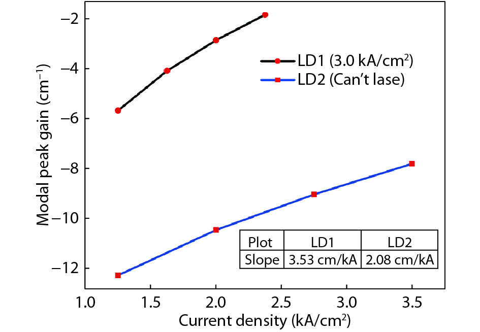
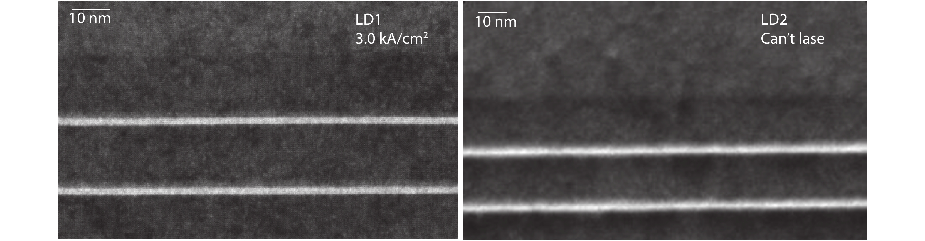
The inhomogeneous broadening parameter and the internal loss of green LDs are determined by experiments and theoretical fitting. It is found that the inhomogeneous broadening plays an important role on the threshold current density of green LDs. The green LD with large inhomogeneous broadening even cannot lase. Therefore, reducing inhomogeneous broadening is a key issue to improve the performance of green LDs.
J. Semicond.
2019, 40(5): 052803 doi: 10.1088/1674-4926/40/5/052803
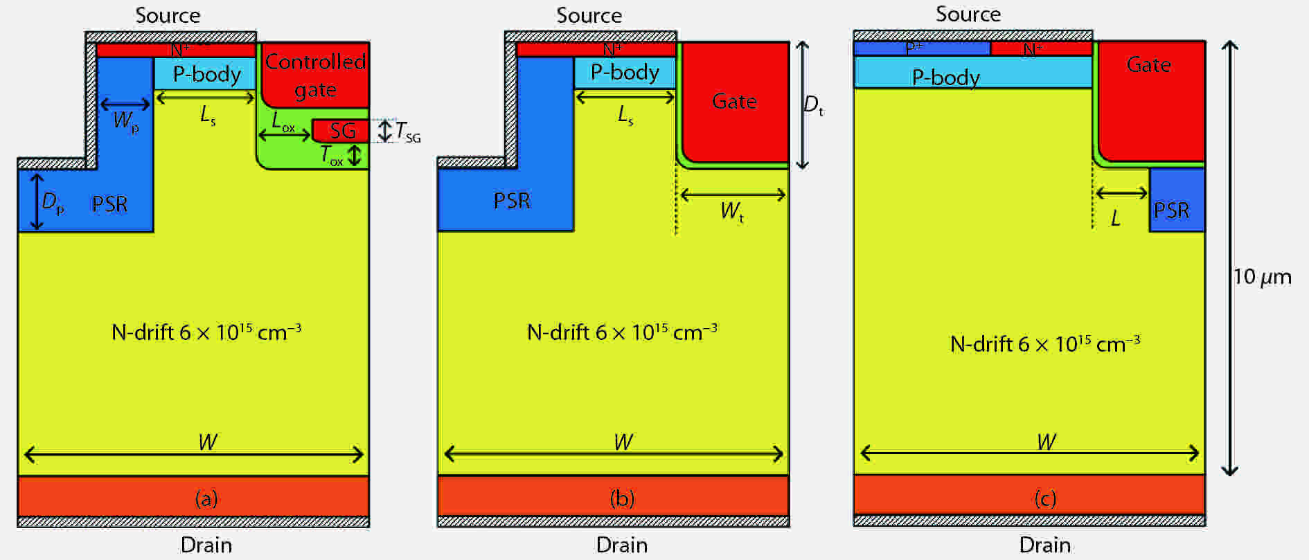
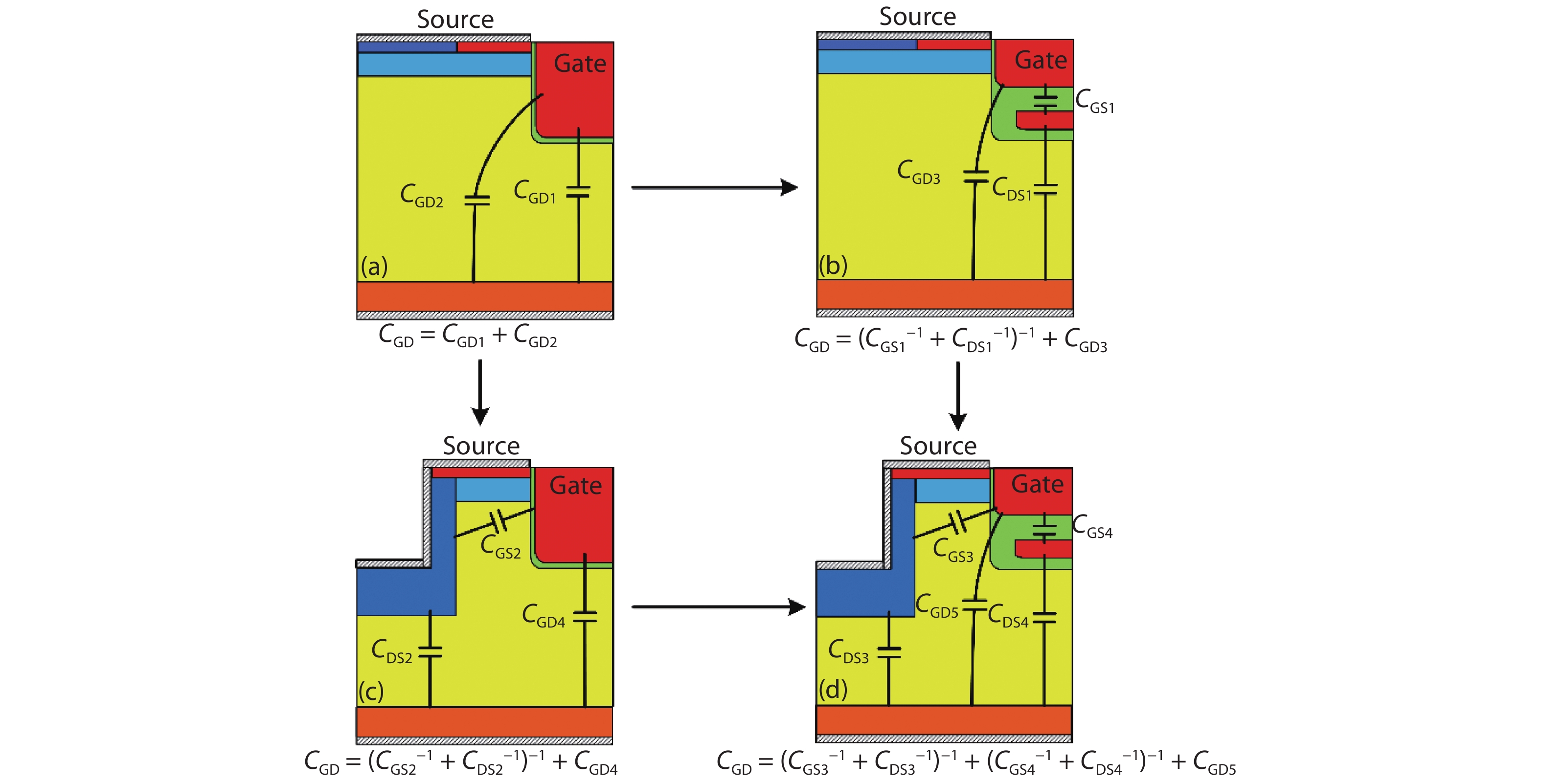
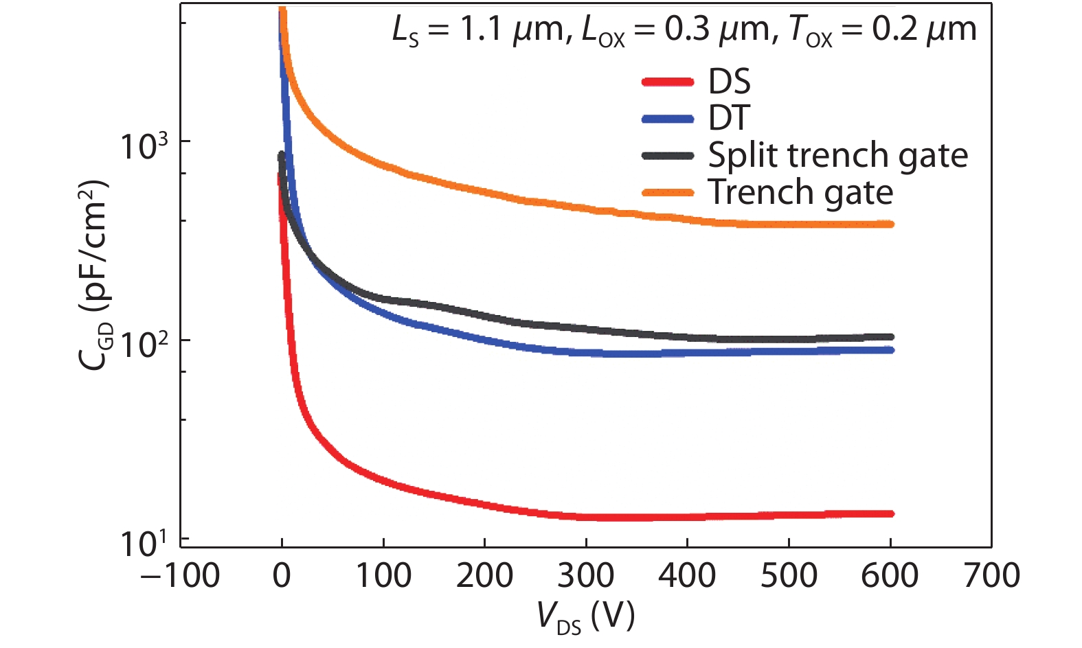
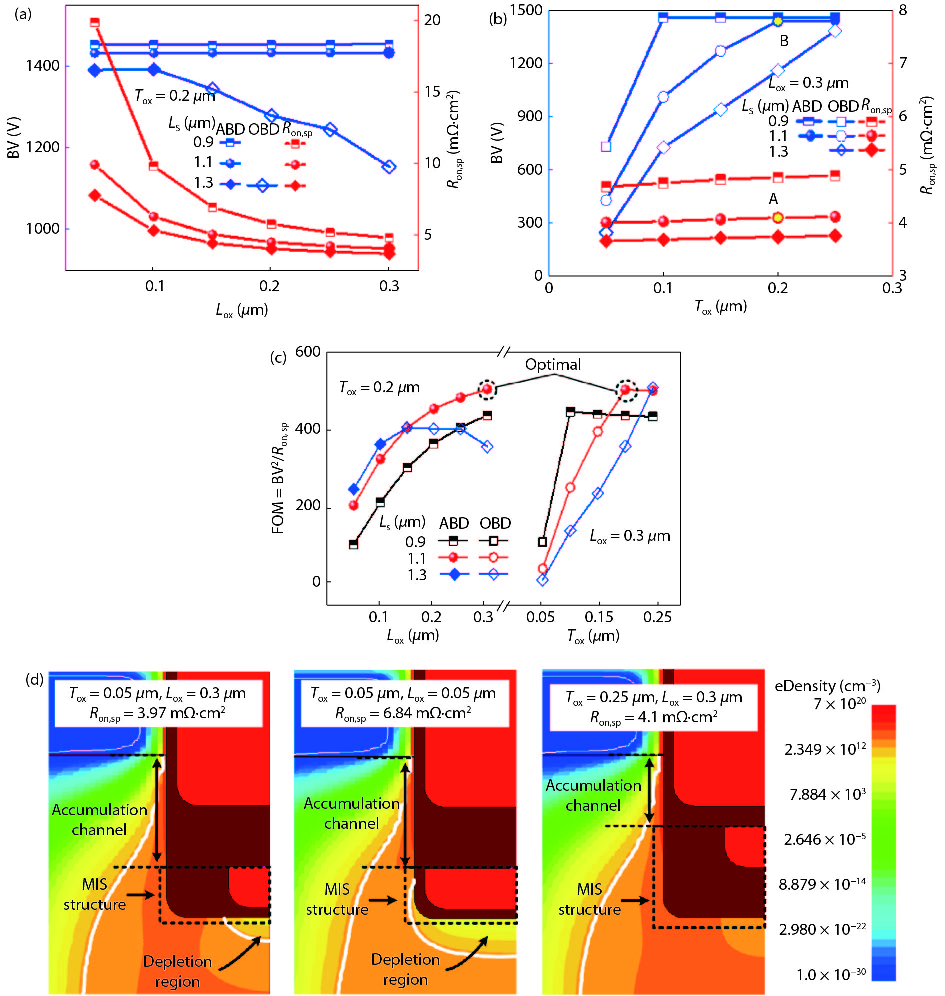
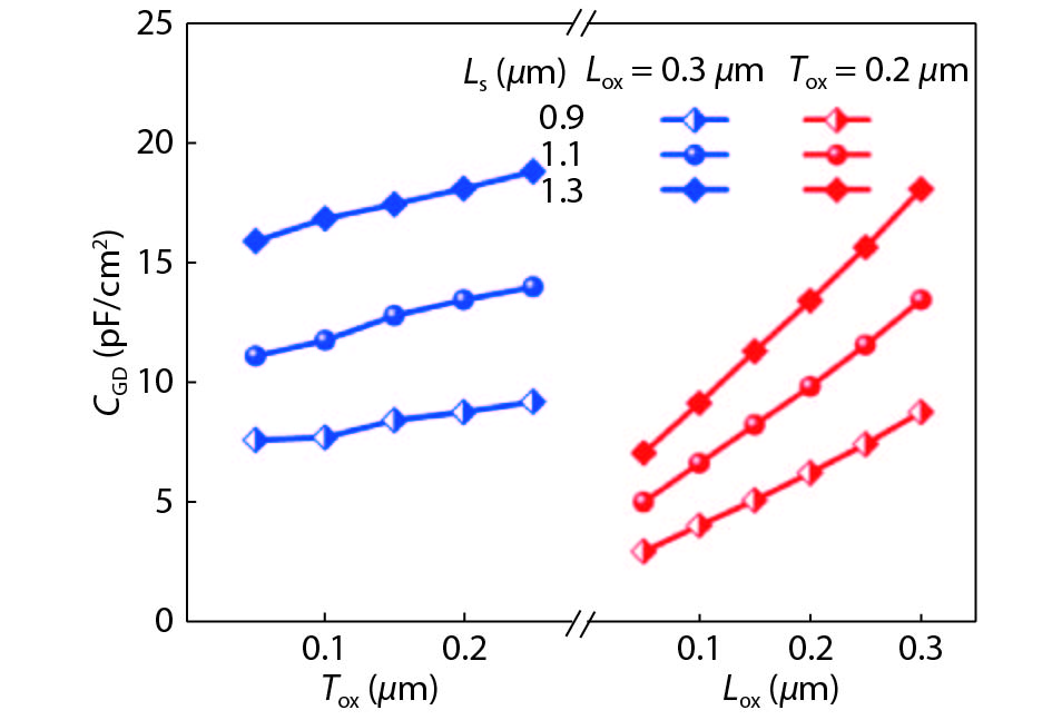
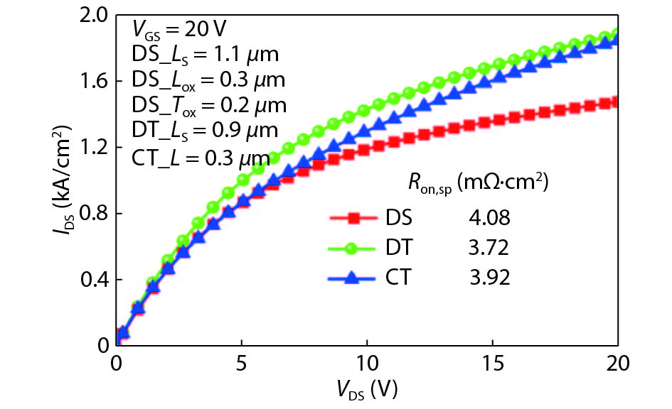
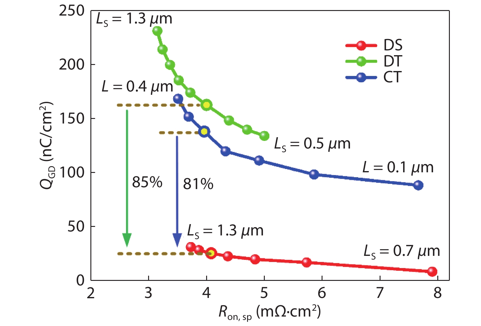
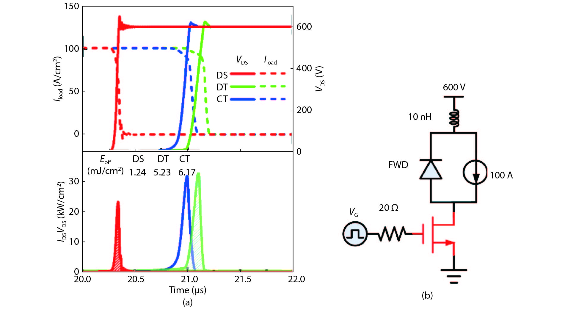
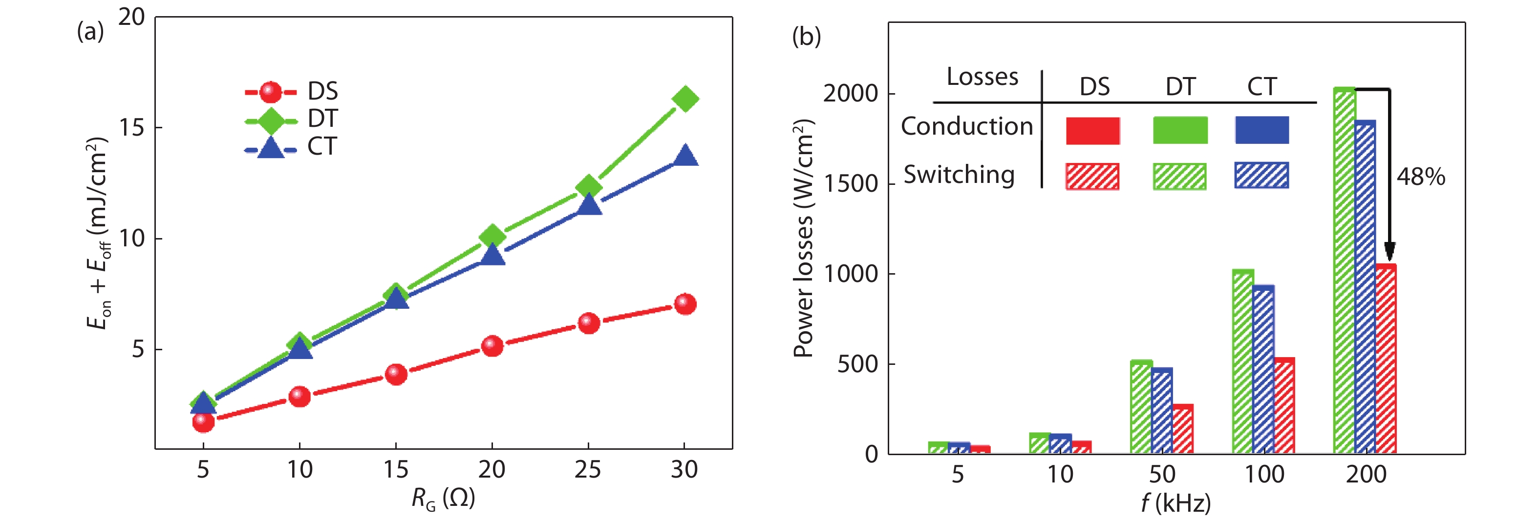
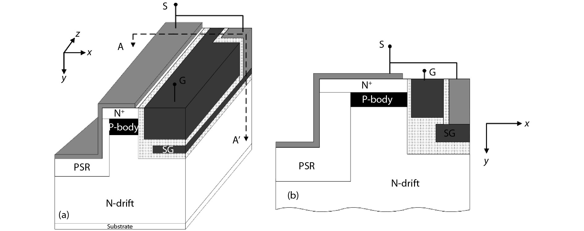
A new ultralow gate–drain charge (QGD) 4H-SiC trench MOSFET is presented and its mechanism is investigated by simulation. The novel MOSFET features double shielding structures (DS-MOS): one is the grounded split gate (SG), the other is the P+ shielding region (PSR). Both the SG and the PSR reduce the coupling effect between the gate and the drain, and transform the most part of the gate–drain capacitance (CGD) into the gate–source capacitance (CGS) and drain–source capacitance (CDS) in series. Thus the CGD is reduced and the proposed DS-MOS obtains ultralow QGD. Compared with the double-trench MOSFET (DT-MOS) and the conventional trench MOSFET (CT-MOS), the proposed DS-MOS decreases the QGD by 85% and 81%, respectively. Moreover, the figure of merit (FOM), defined as the product of specific on-resistance (Ron, sp) and QGD (Ron, spQGD), is reduced by 84% and 81%, respectively.


J. Semicond.
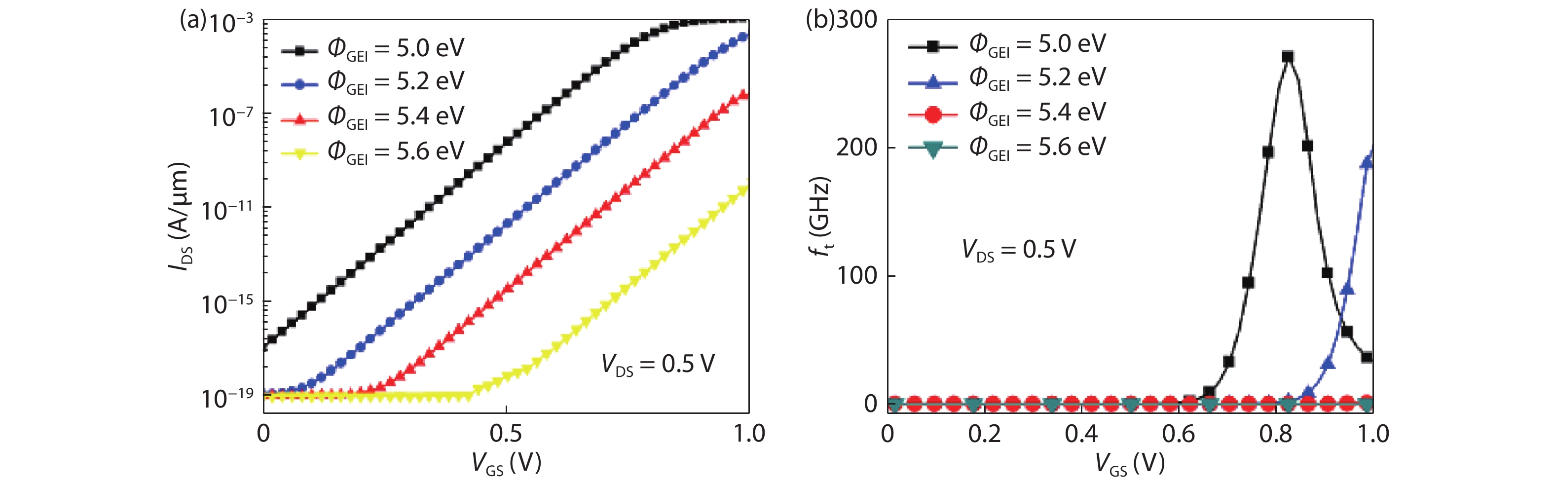
2019, 40(5): 052901 doi: 10.1088/1674-4926/40/5/052901

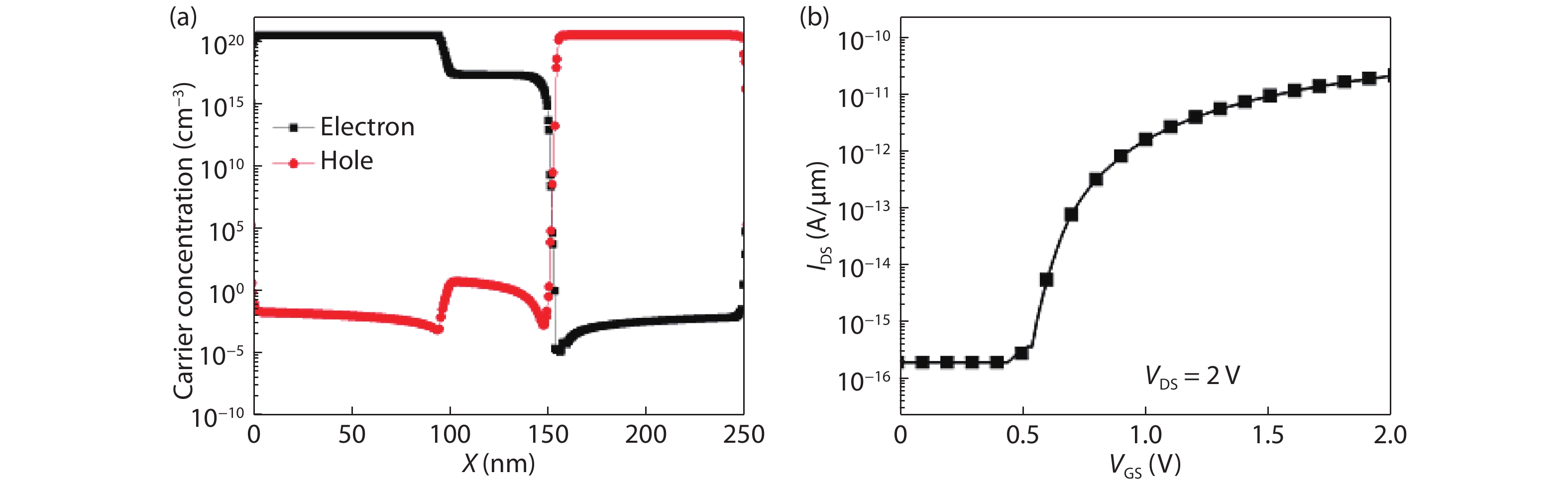
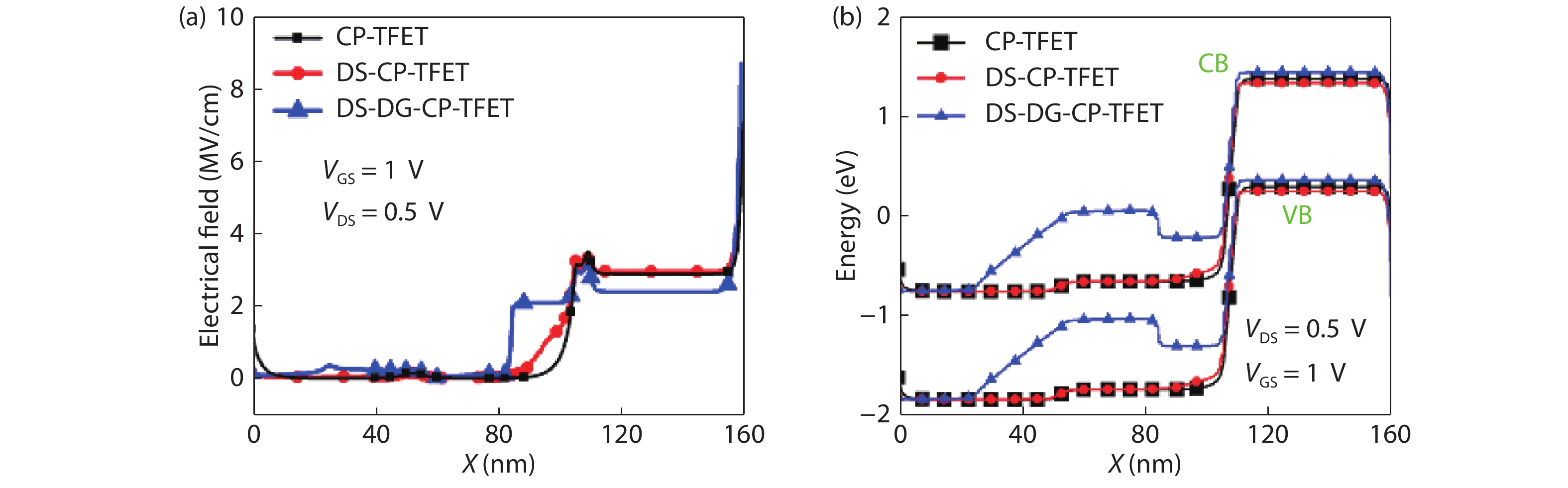
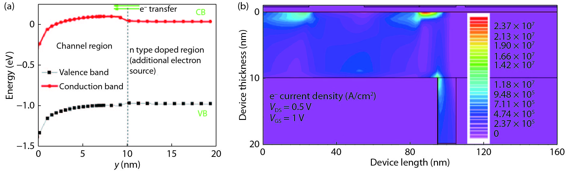
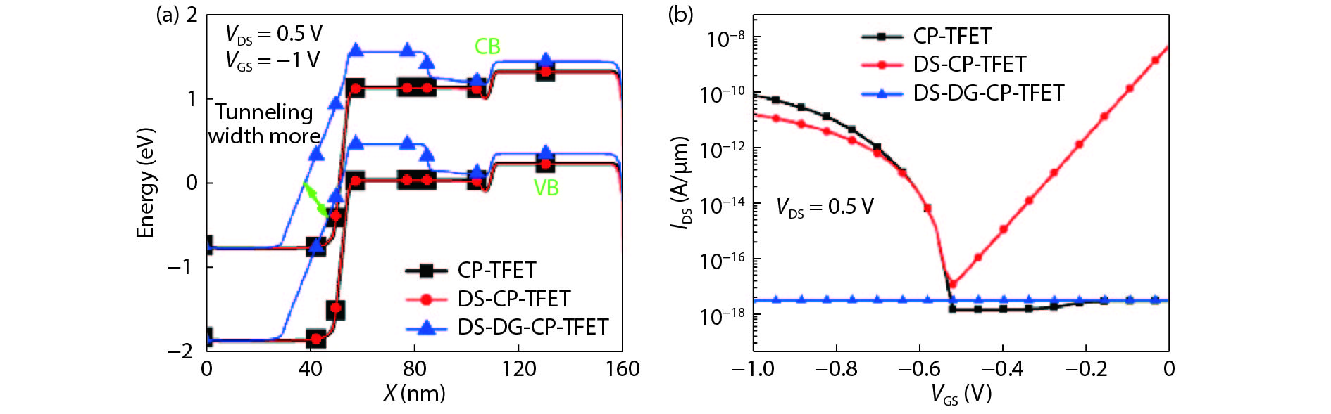
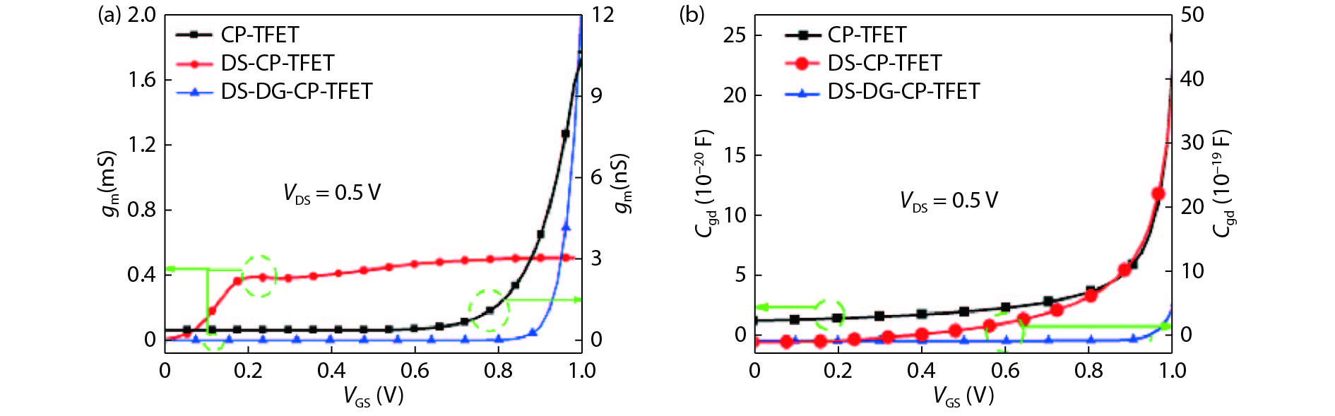
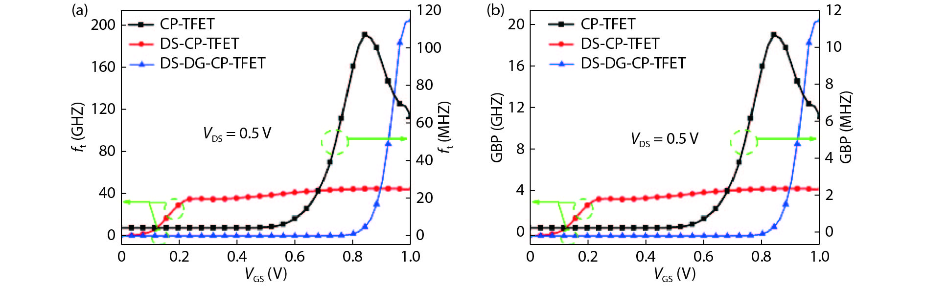
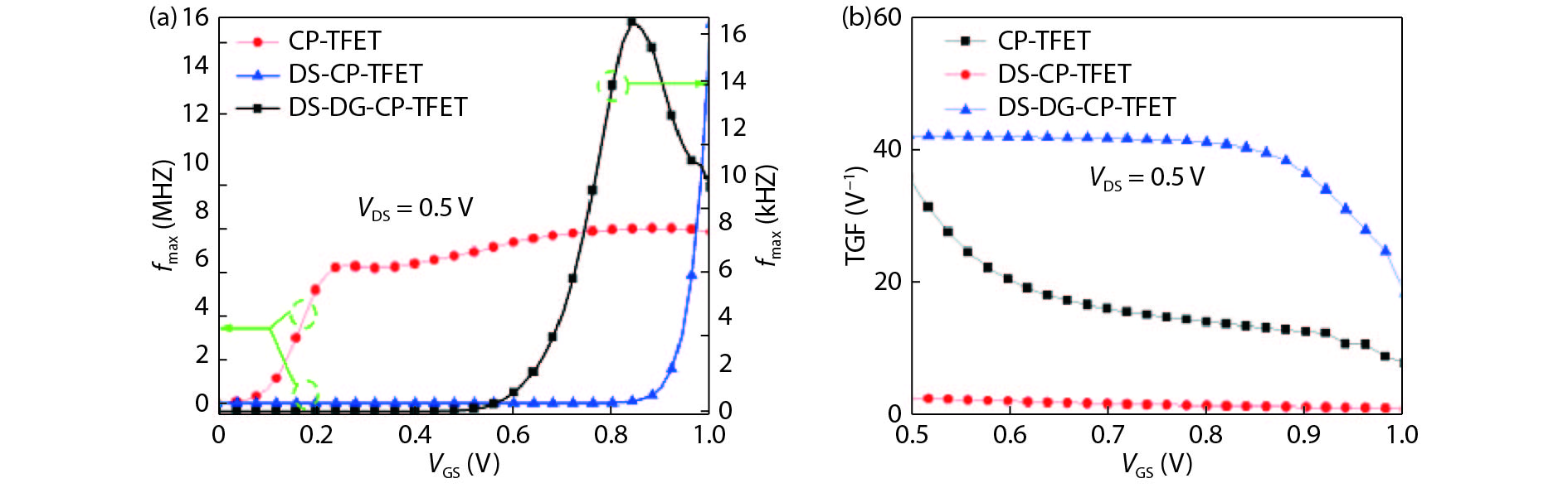
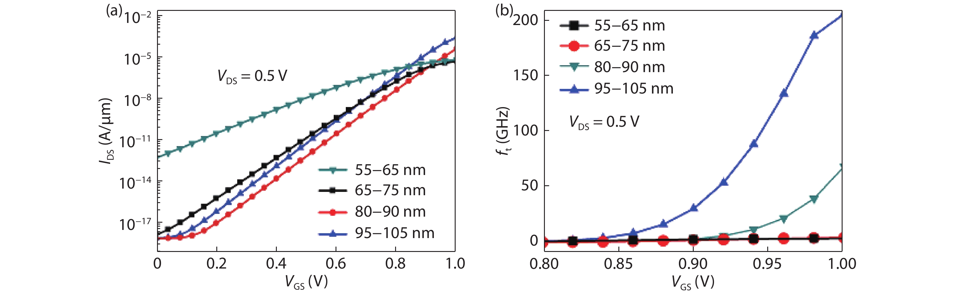
In this paper, the impact of extra electron source (EES) and dual metal gate engineering on conventional charge plasma TFET (CP-TFET) have been done for improving DC and analog/RF parameters. CP-TFET structure is upgraded to double source CP-TFET (DS-CP-TFET) by placing an EES below the source/channel junction for enhancing the device performance in terms of driving current and RF figures of merit (FOMs). But, in spite of these pros, the approach is having cons of higher leakage current similar to MOSFET and negative conductance (inherent nature of TFET). Both the issues have been resolved in the double source dual gate CP-TFET (DS-DG-CP-TFET) by gate workfunction engineering and drain underlapping respectively. Additionally, for getting the optimum performance of DS-DG-CP-TFET, the device sensitivity has been investigated in terms of position of EES, length of drain electrode and workfunction of gate electrode 1 (GE1).