Issue Browser
Volume 43, Issue 9,
Sep 2022
Column
J. Semicond.
2022, 43(9): 093101 doi: 10.1088/1674-4926/43/9/093101

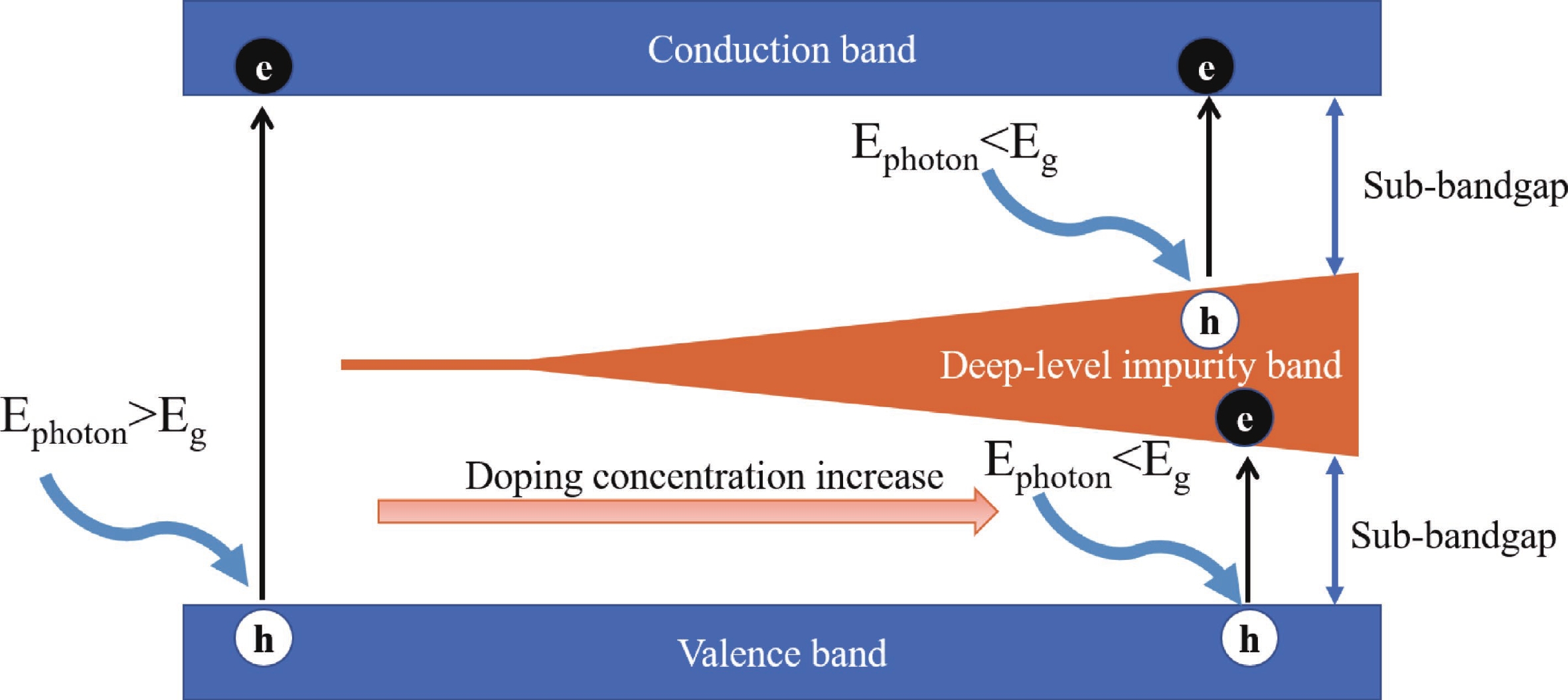
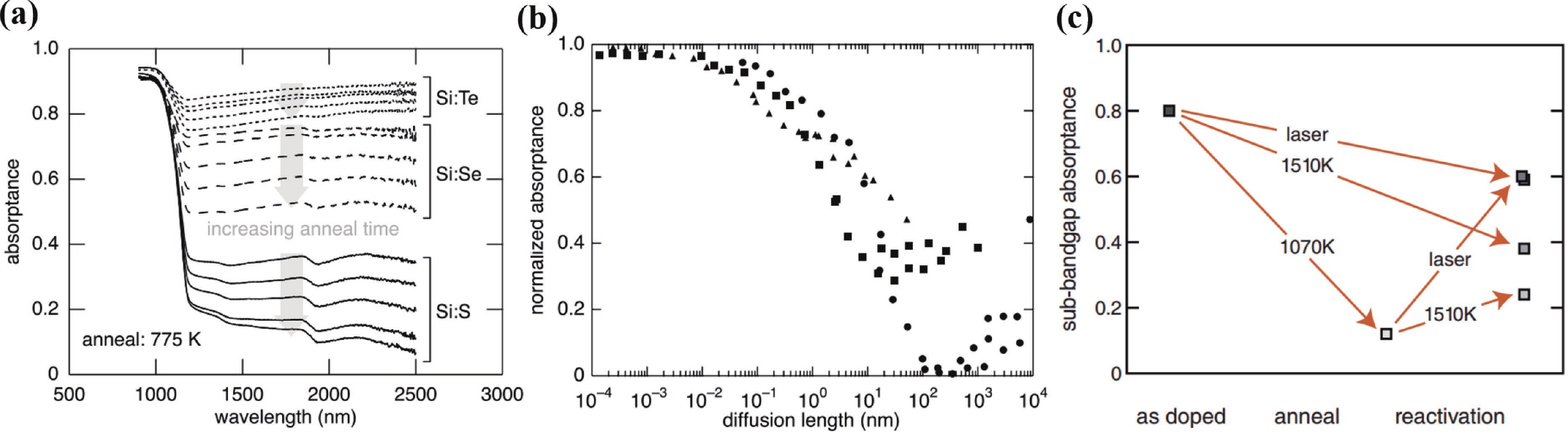
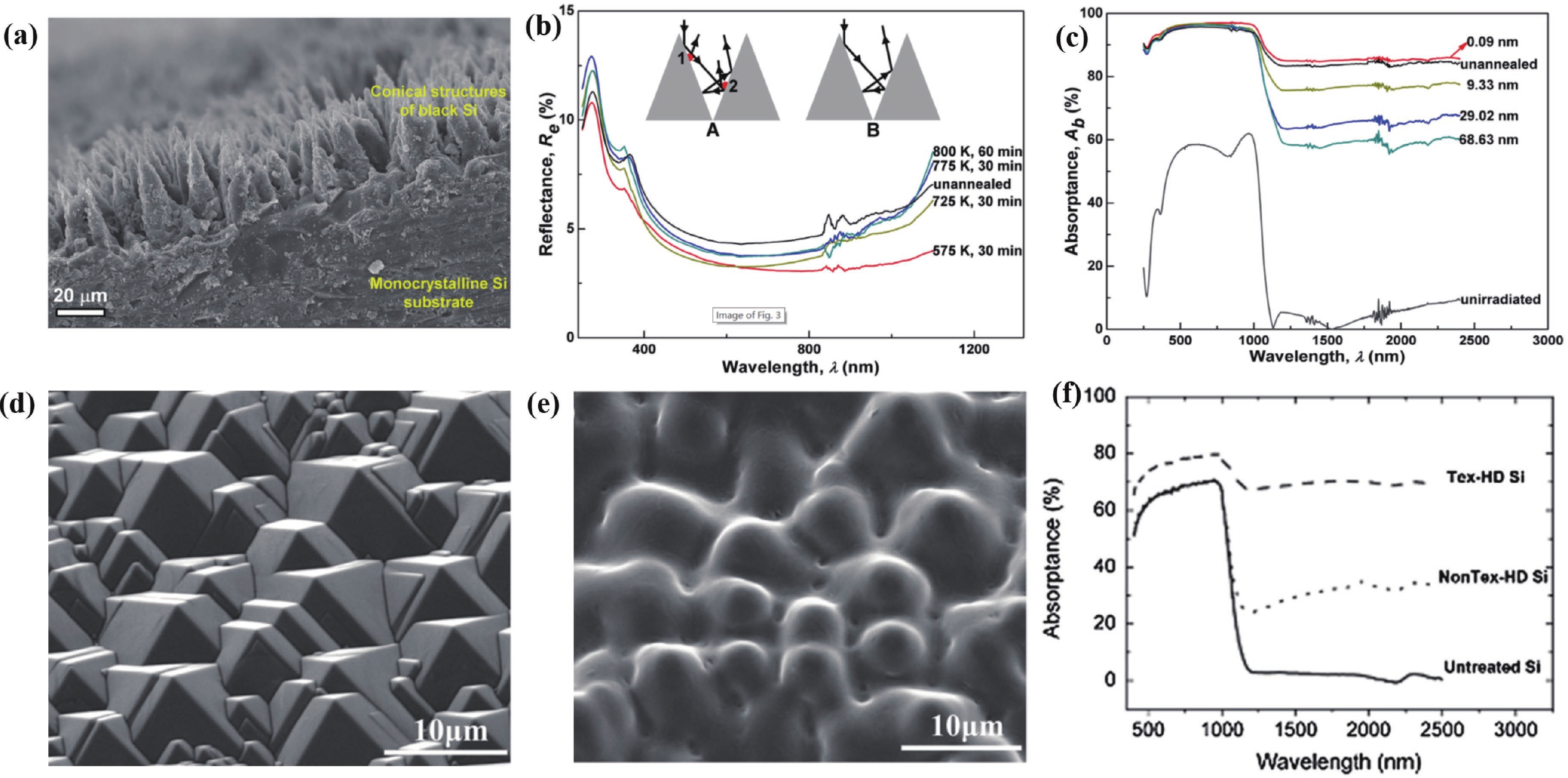
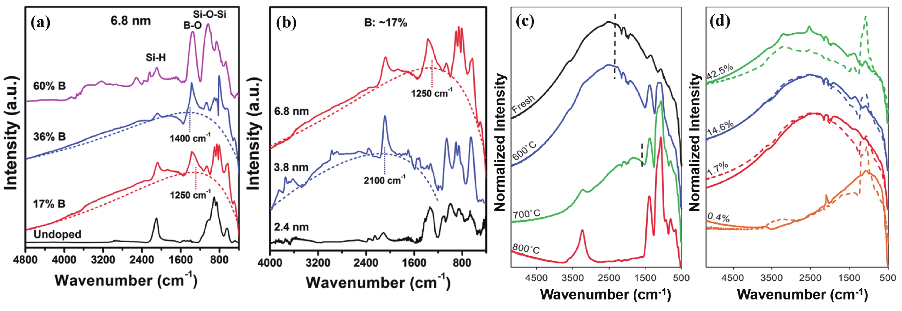
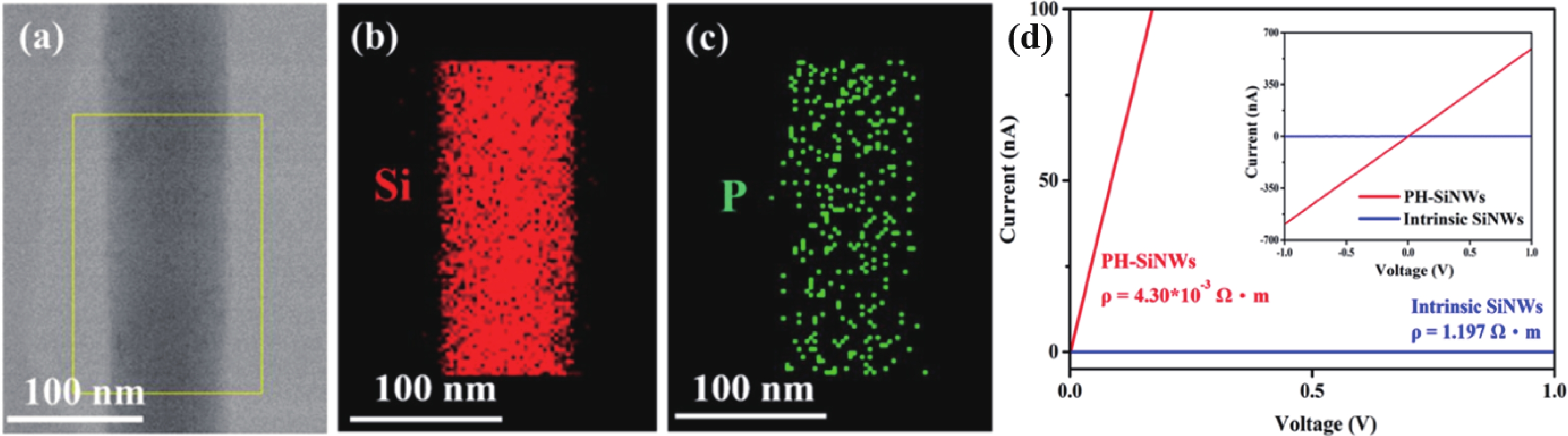
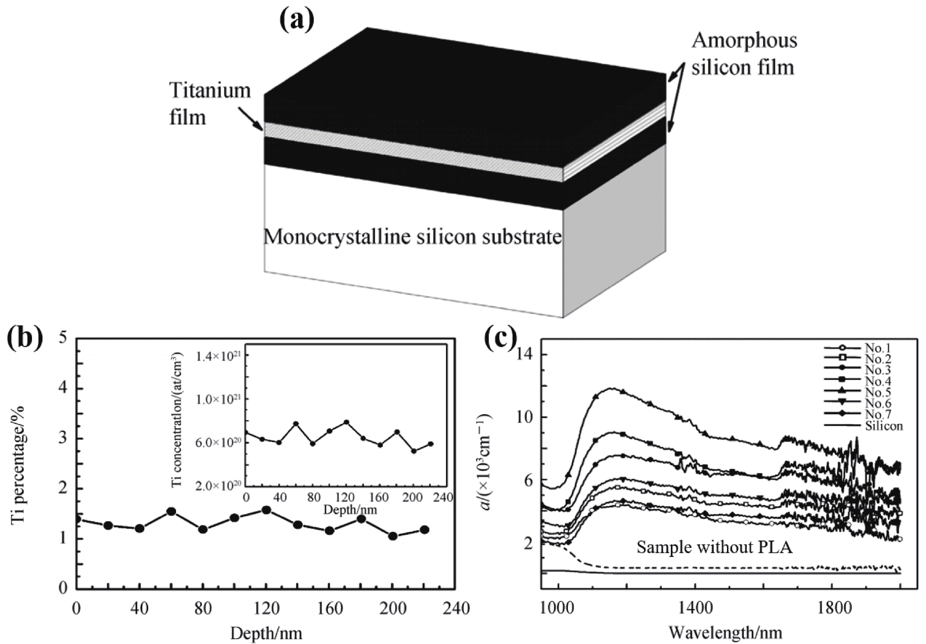
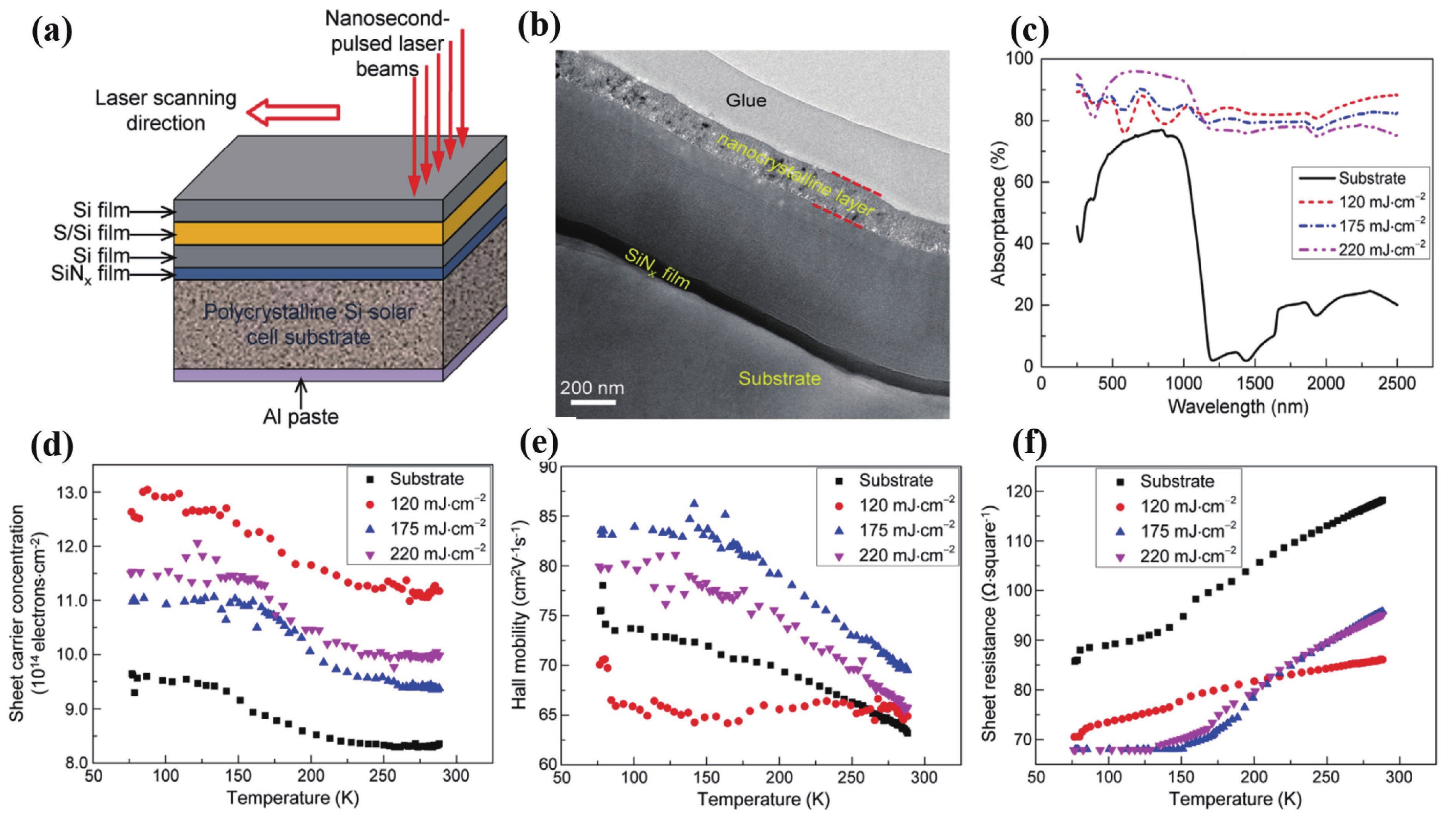
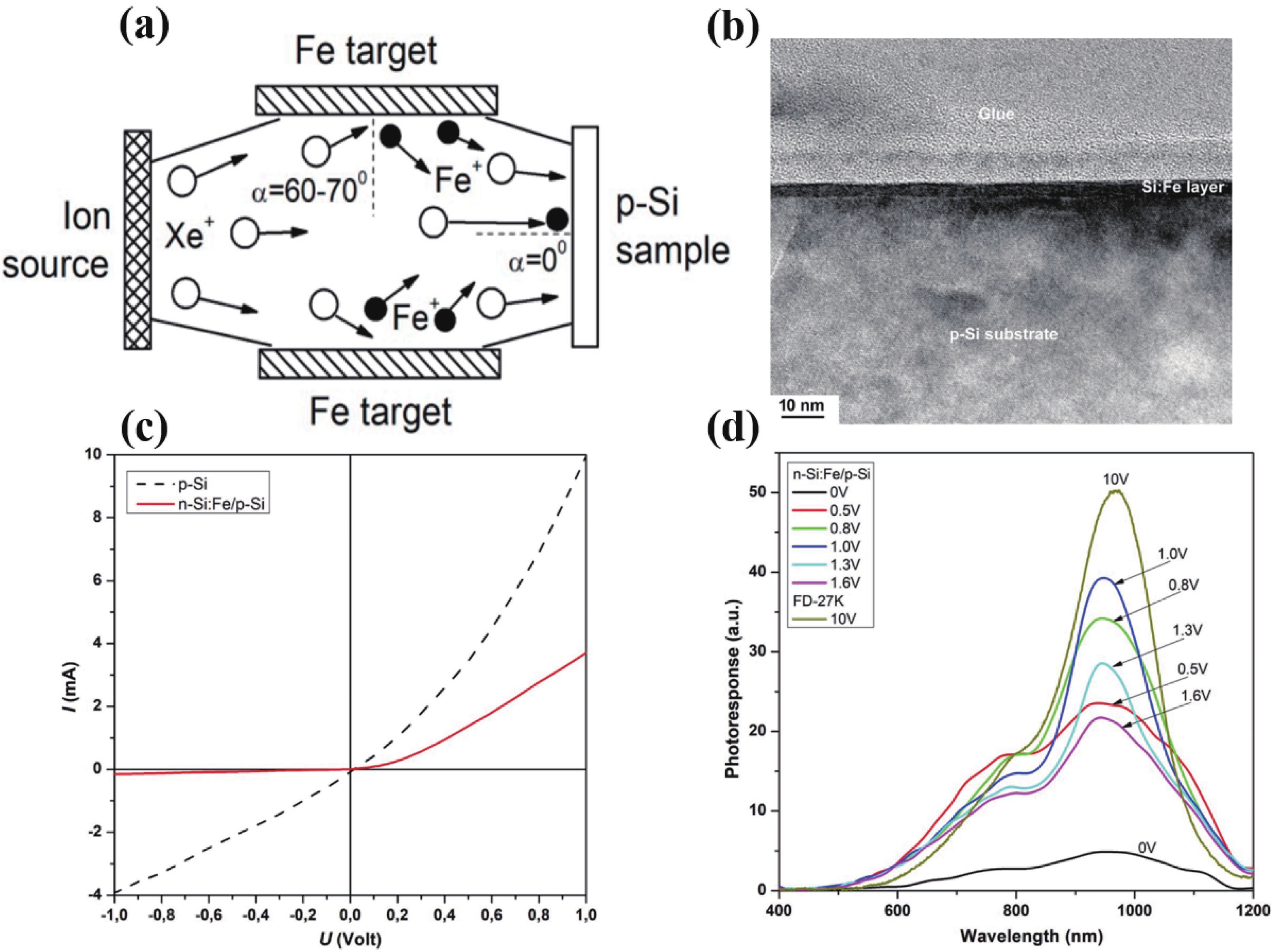
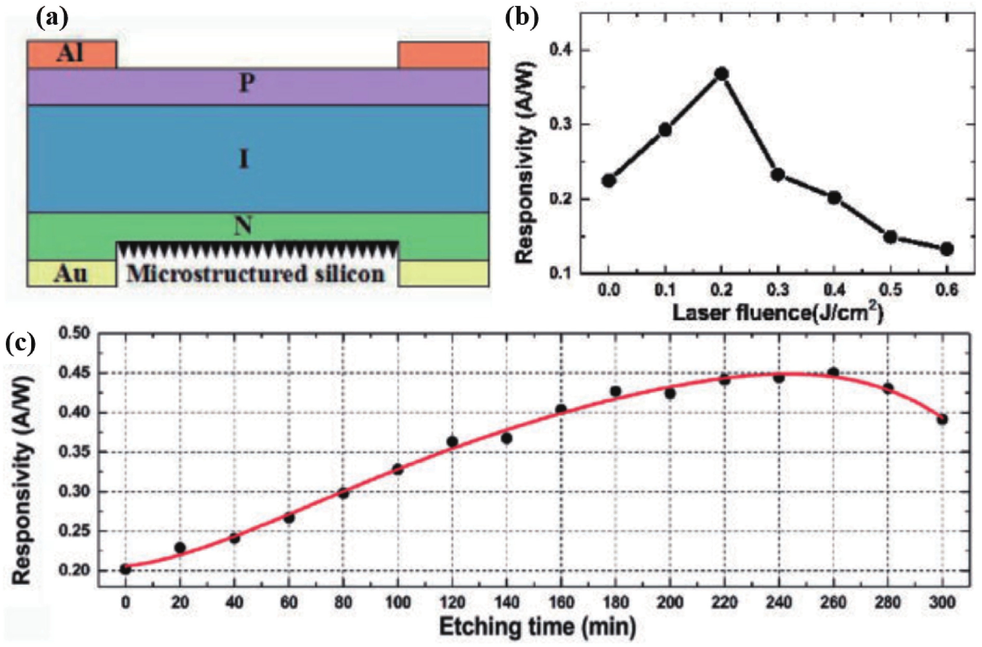
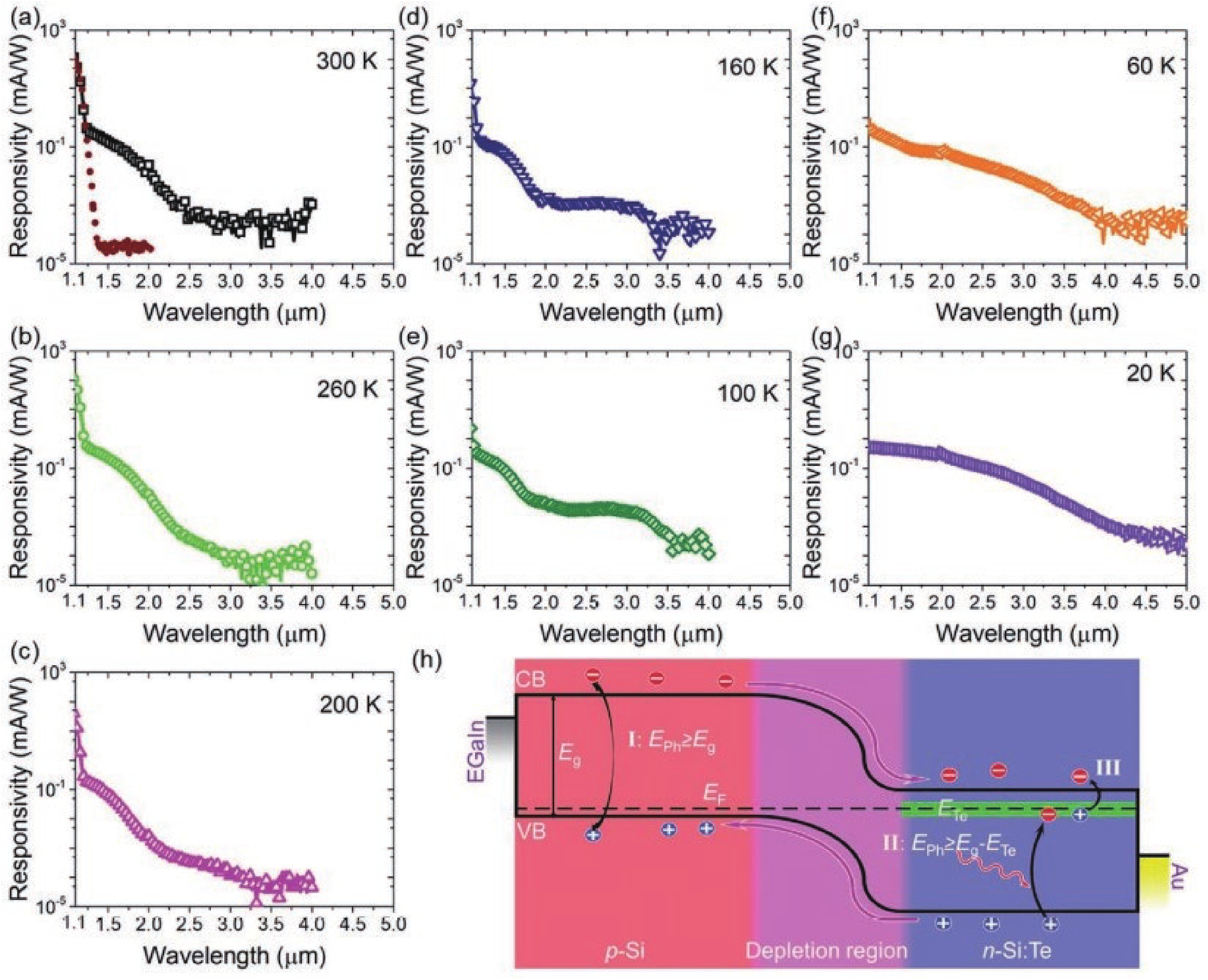
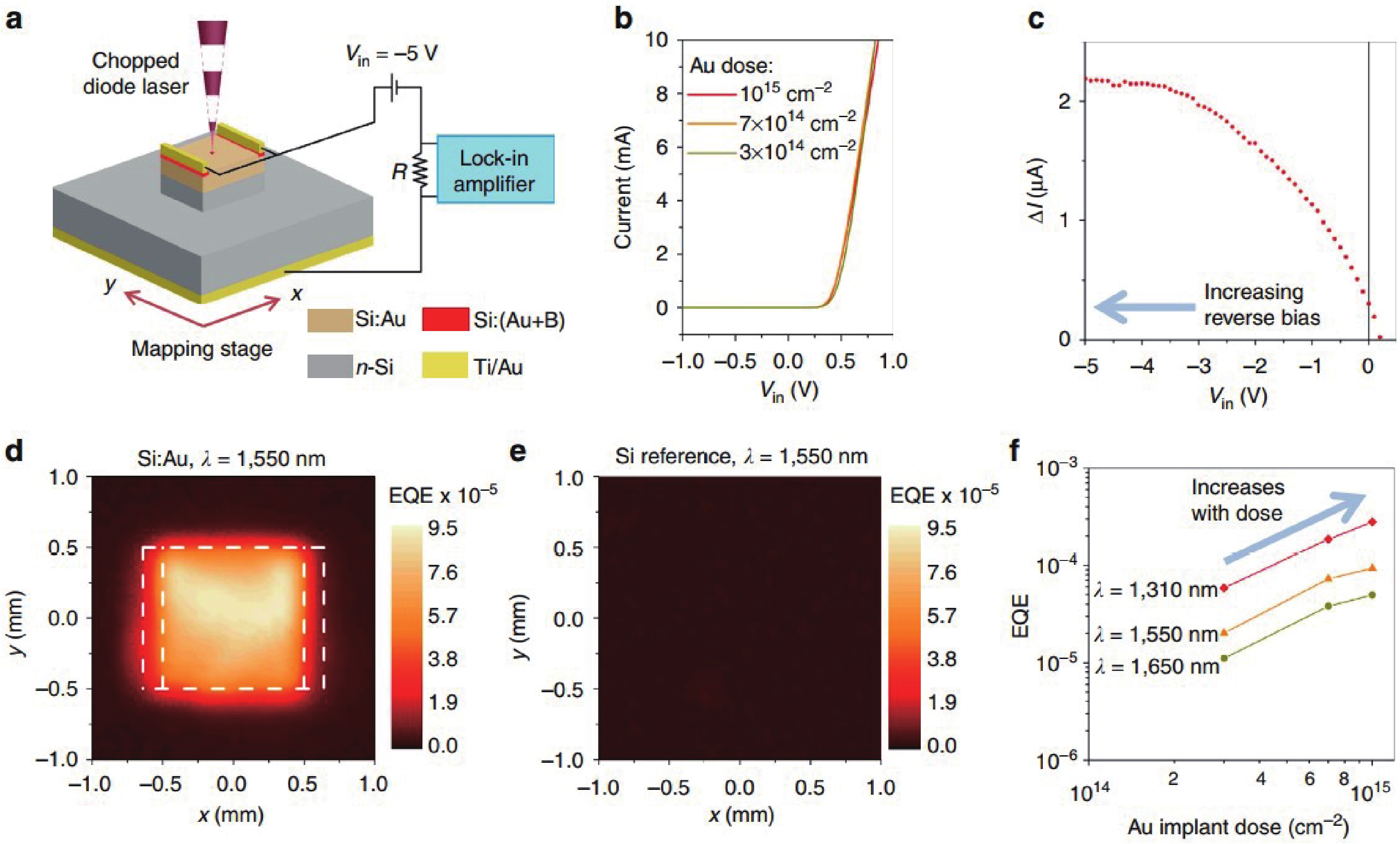
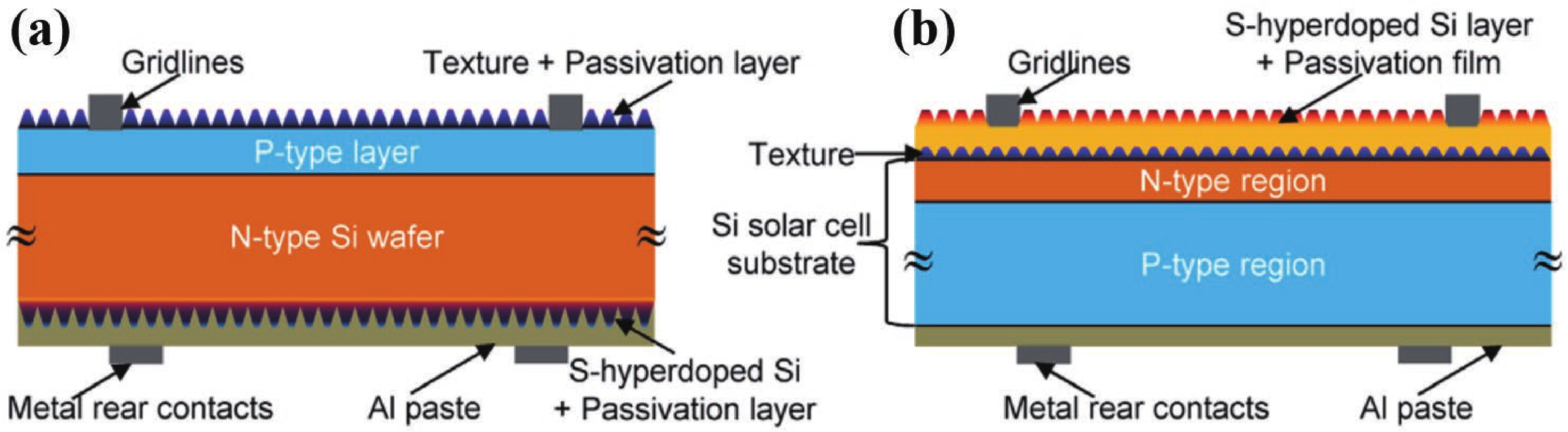
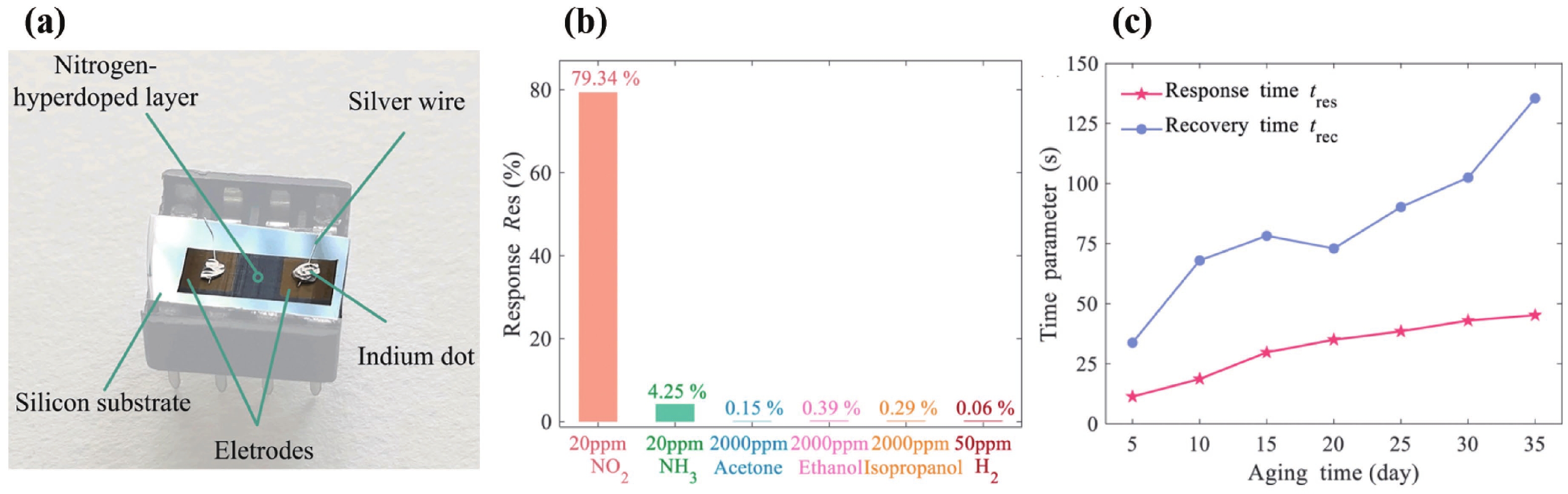
Hyperdoping that introduces impurities with concentrations exceeding their equilibrium solubility has been attracting great interest since the tuning of semiconductor properties increasingly relies on extreme measures. In this review we focus on hyperdoped silicon (Si) by introducing methods used for the hyperdoping of Si such as ion implantation and laser doping, discussing the electrical and optical properties of hyperdoped bulk Si, Si nanocrystals, Si nanowires and Si films, and presenting the use of hyperdoped Si for devices like infrared photodetectors and solar cells. The perspectives of the development of hyperdoped Si are also provided.

J. Semicond.
2022, 43(9): 092301 doi: 10.1088/1674-4926/43/9/092301
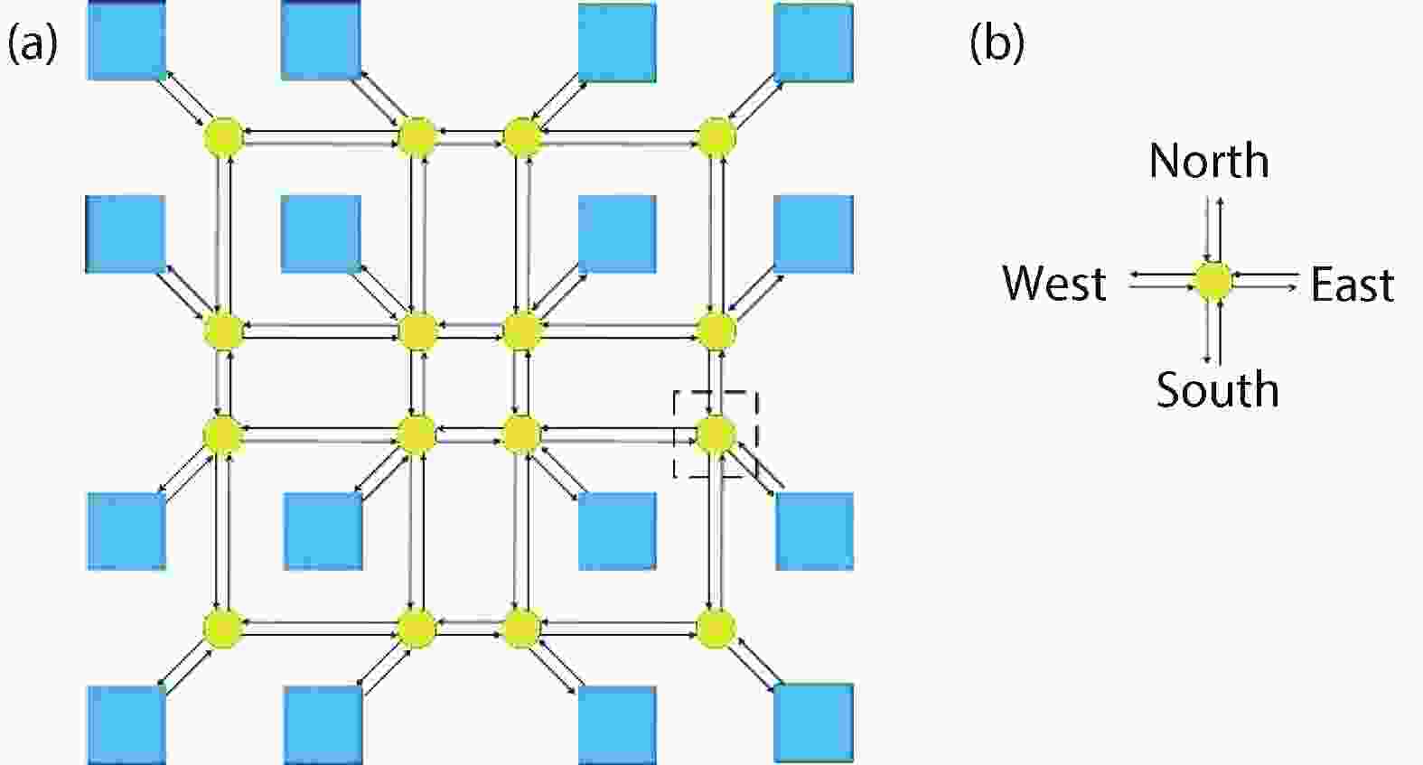
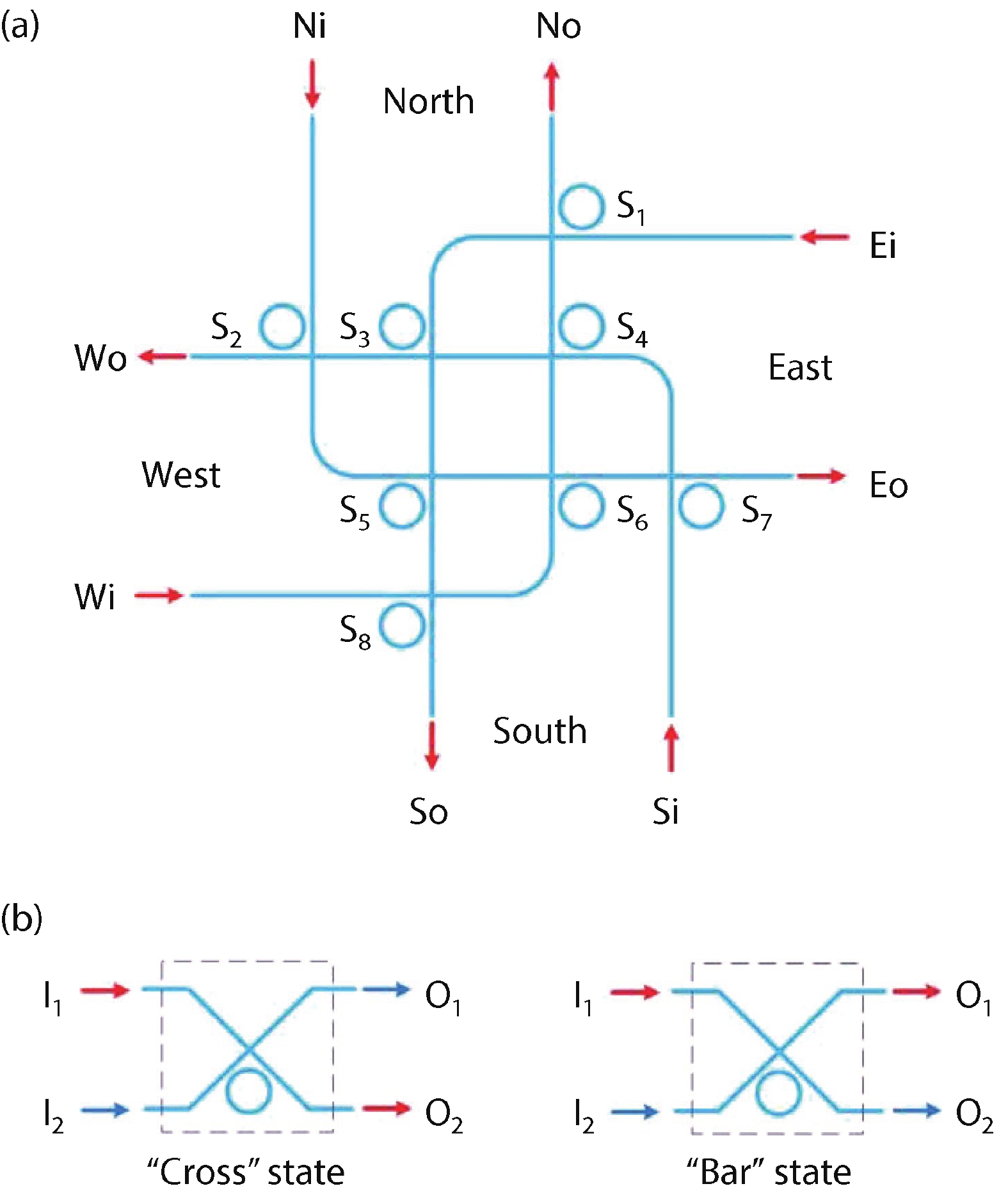
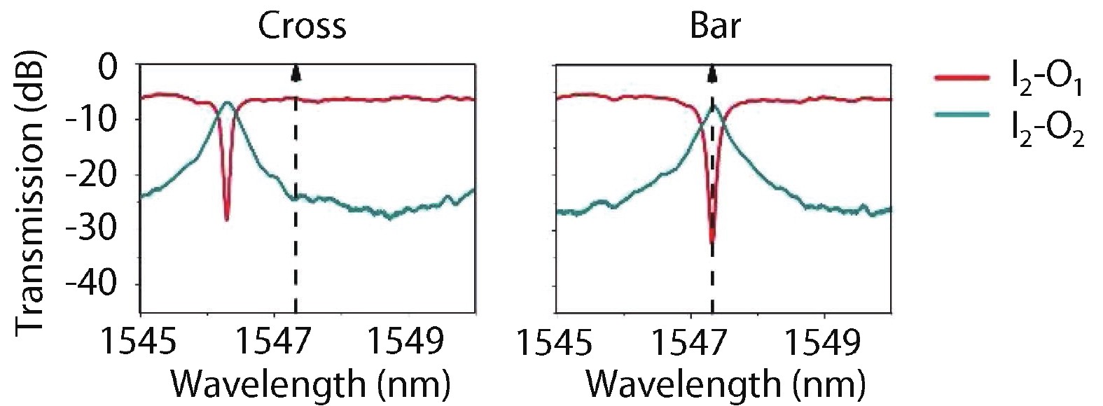
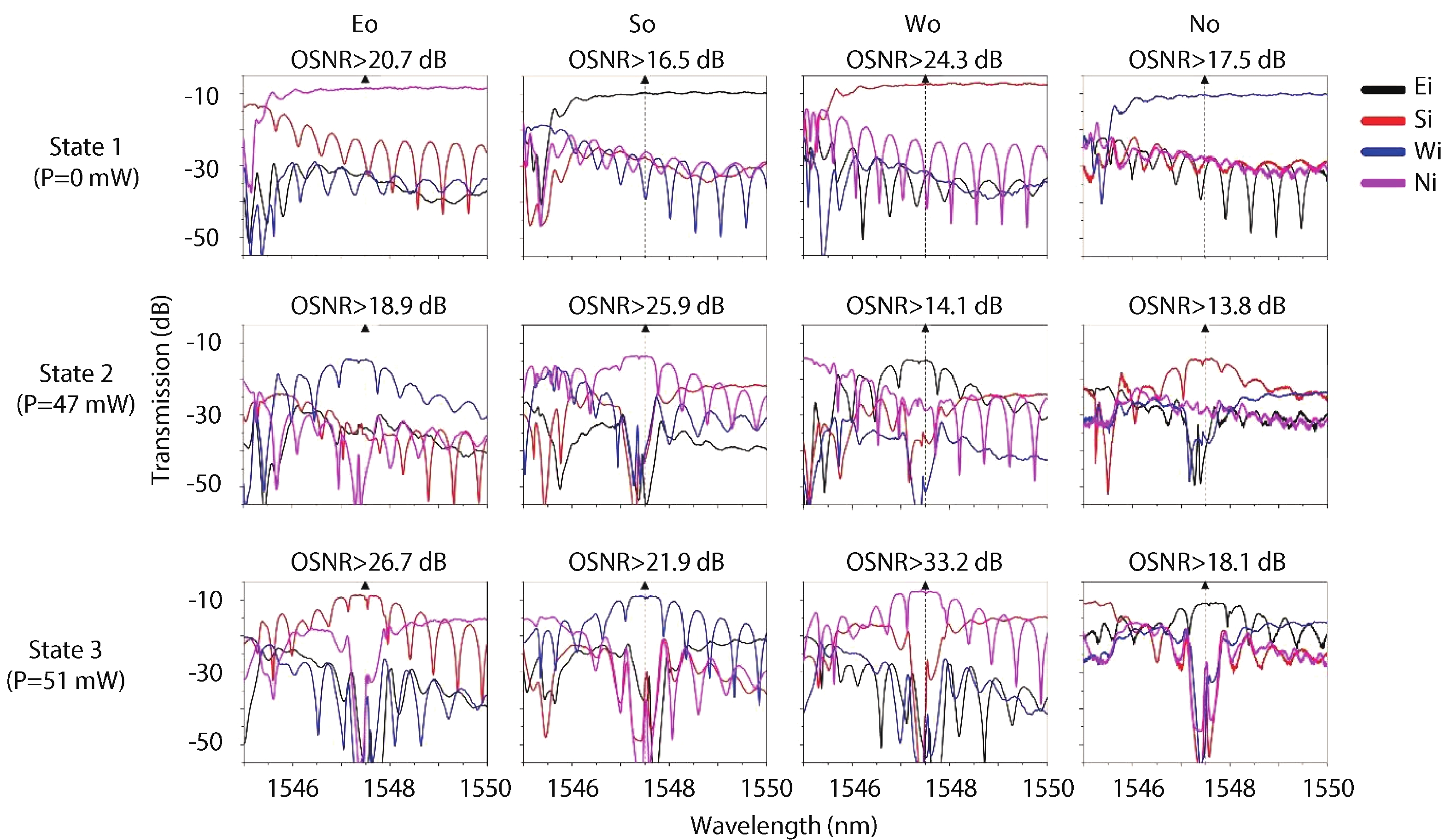
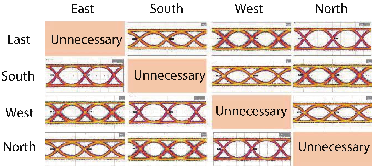
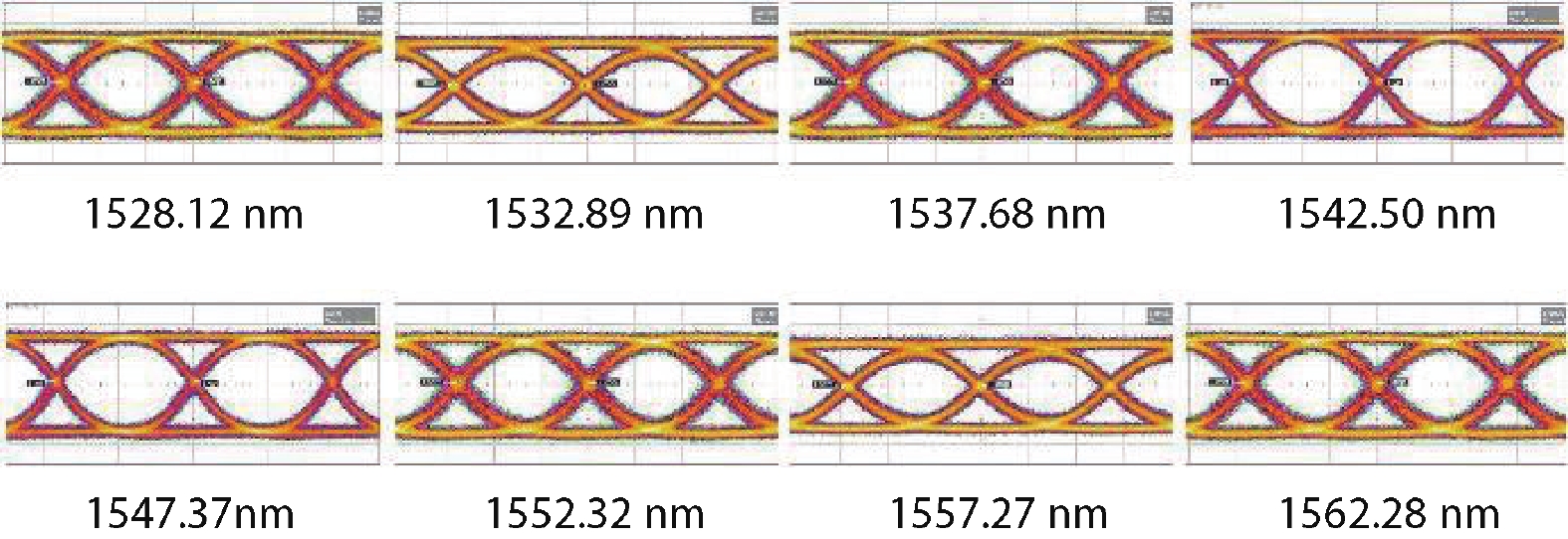
We report a strict non-blocking four-port optical router that is used for a mesh photonic network-on-chip on a silicon-on-insulator platform. The router consists of eight silicon microring switches that are tuned by the thermo-optic effect. For each tested rousting state, the signal-to-noise ratio of the optical router is larger than 13.8 dB at the working wavelength. The routing functionality of the device is verified. We perform 40 Gbps nonreturn to zero code data transmission on its 12 optical links. Meanwhile, data transmission using wavelength division multiplexing on eight channels in the C band (from 1525 to 1565 nm) has been adopted to increase the communication capacity. The optical router’s average energy efficiency is 25.52 fJ/bit. The rising times (10% to 90%) of the eight optical switch elements are less than 10 µs and the falling times (90%–10%) are less than 20 µs.

J. Semicond.
2022, 43(9): 092302 doi: 10.1088/1674-4926/43/9/092302
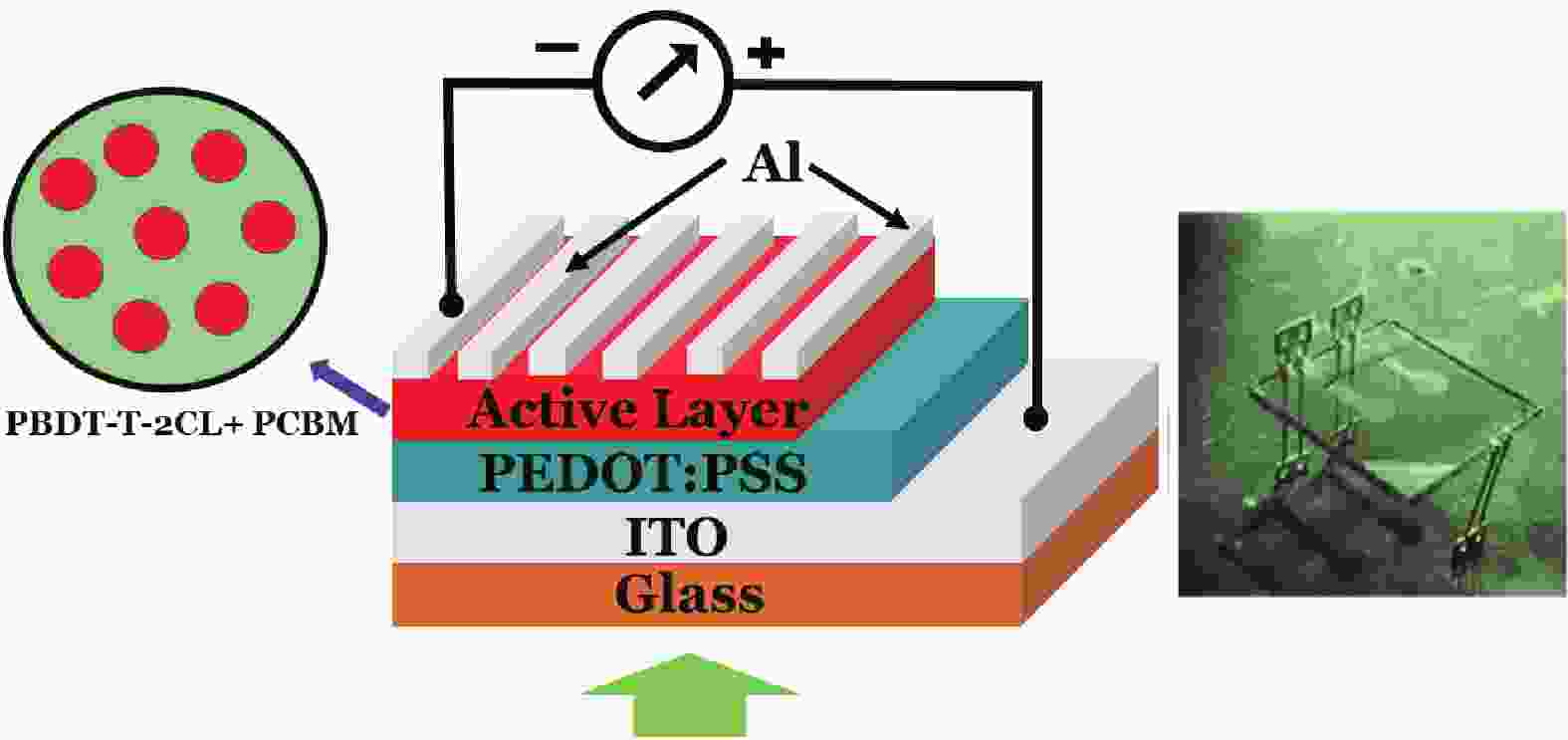
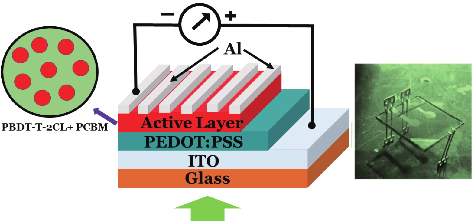
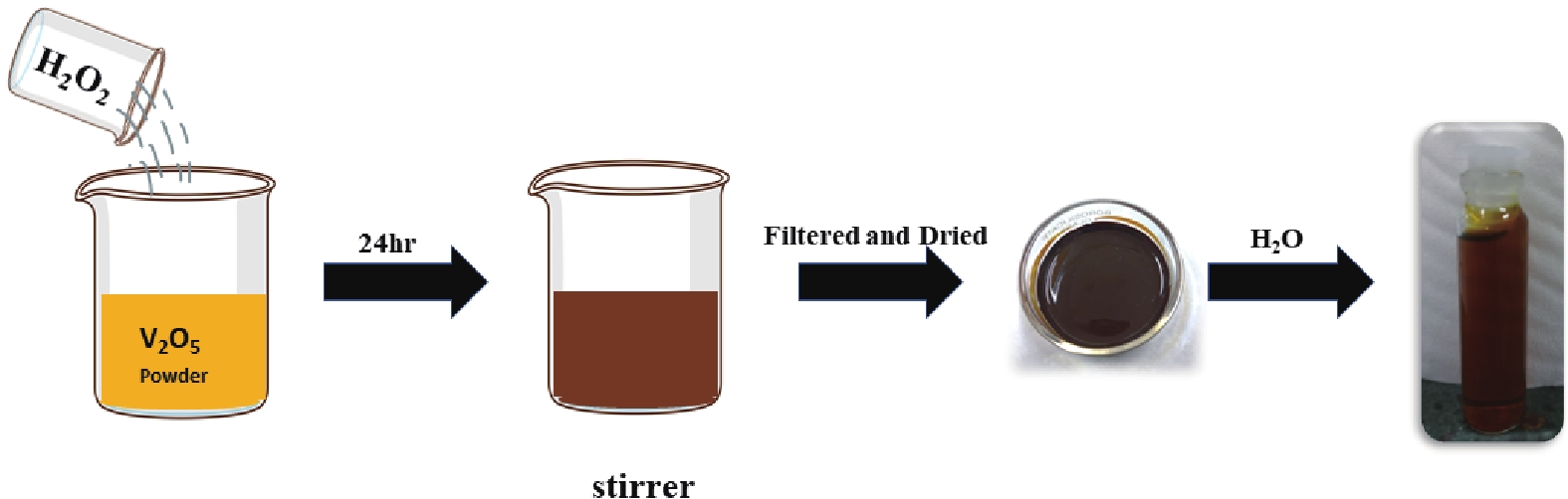
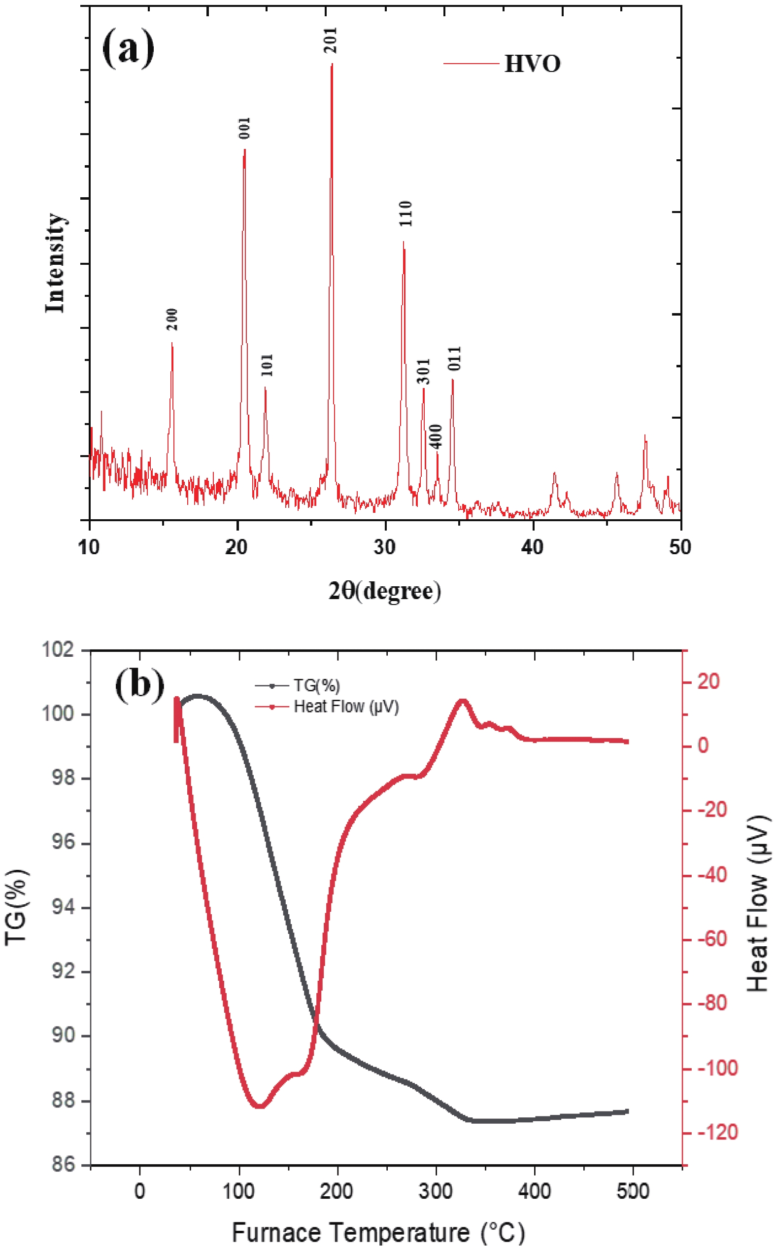
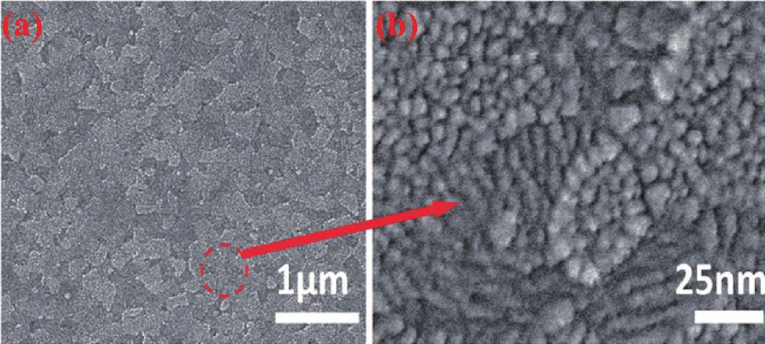
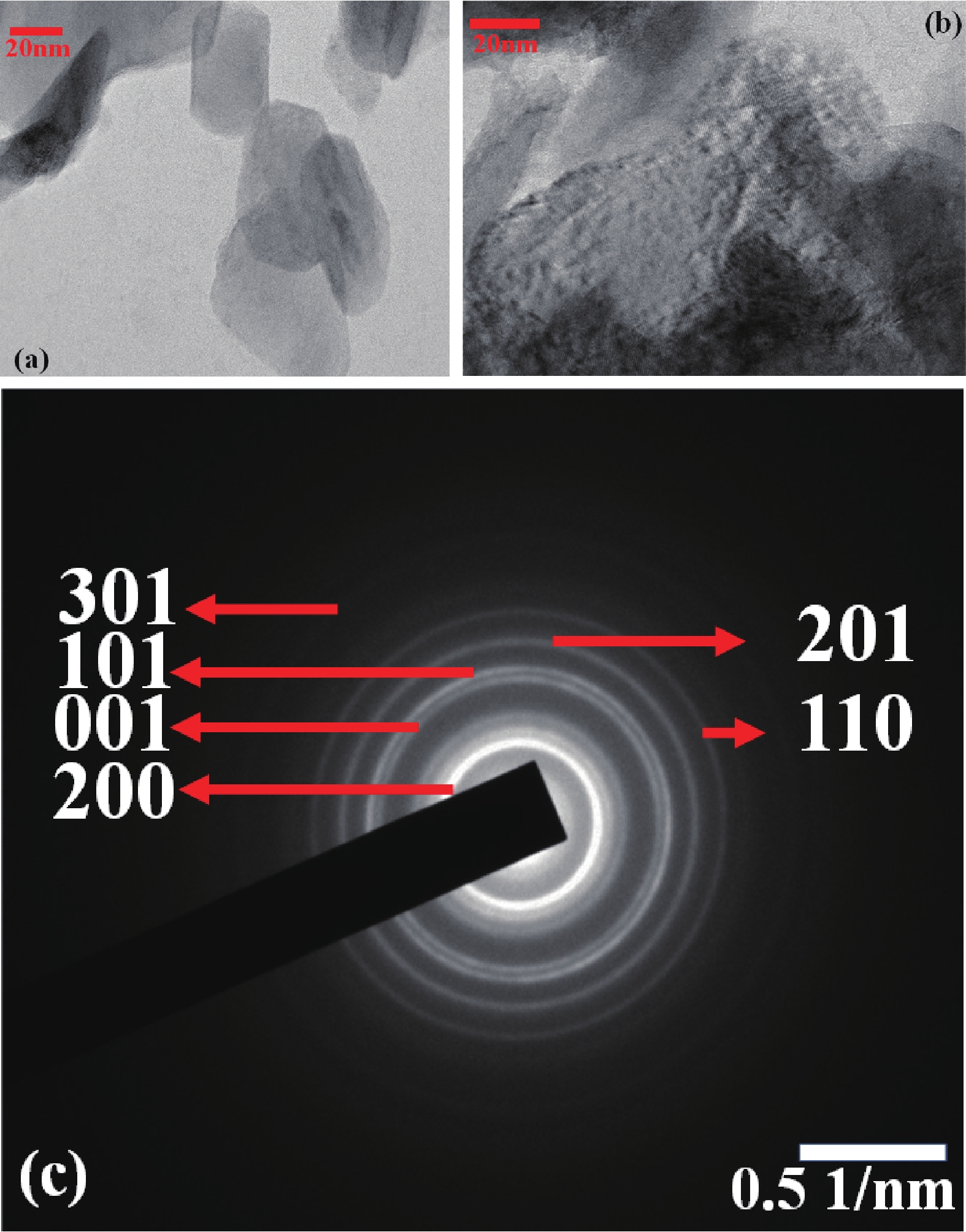
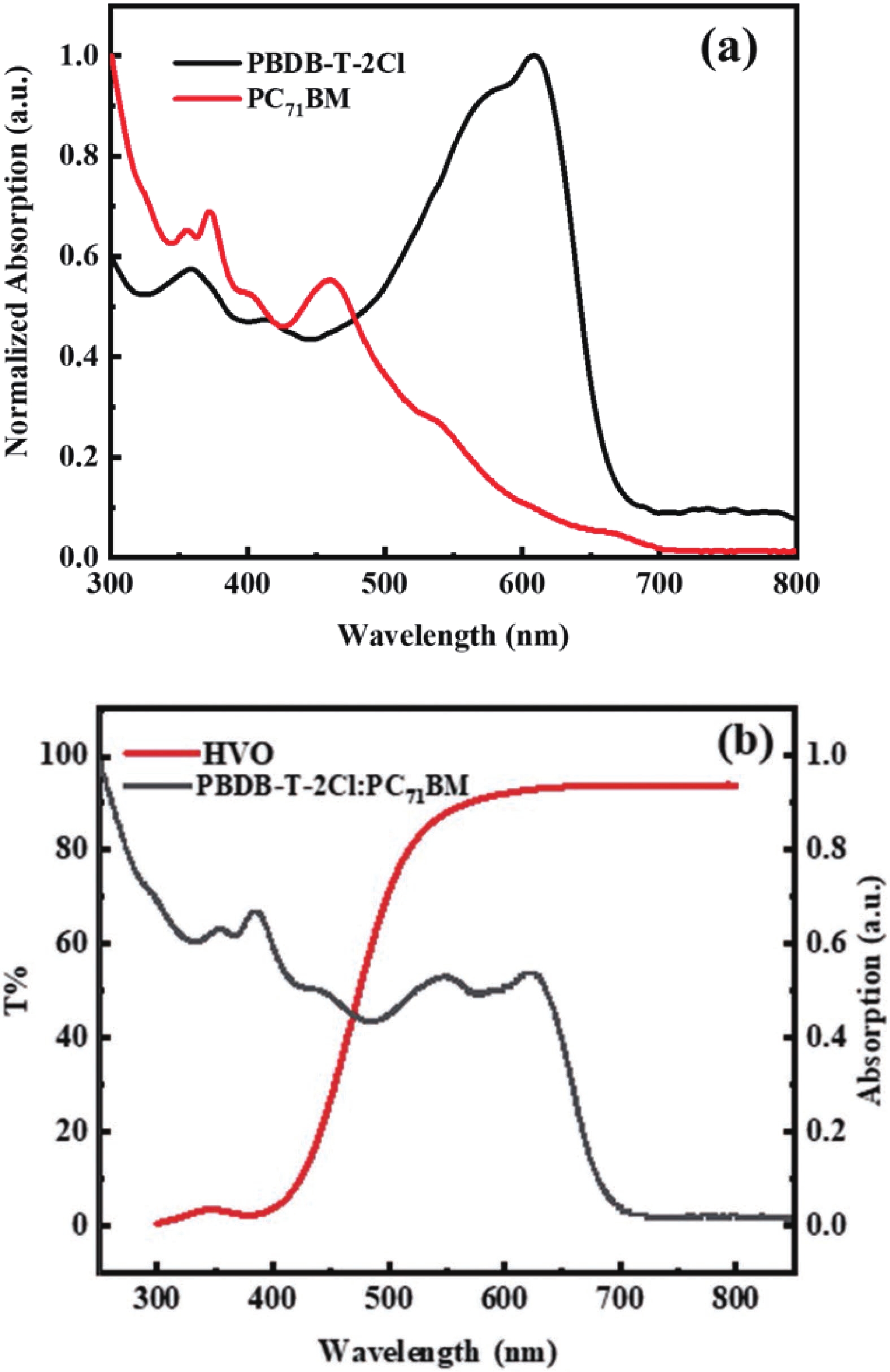
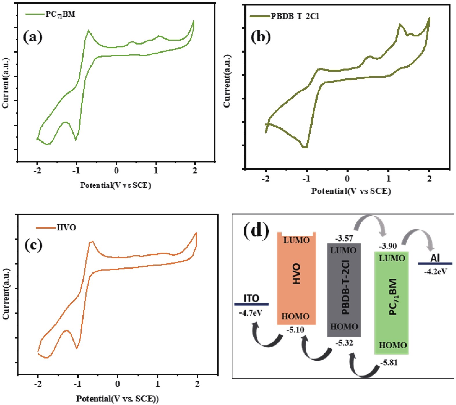
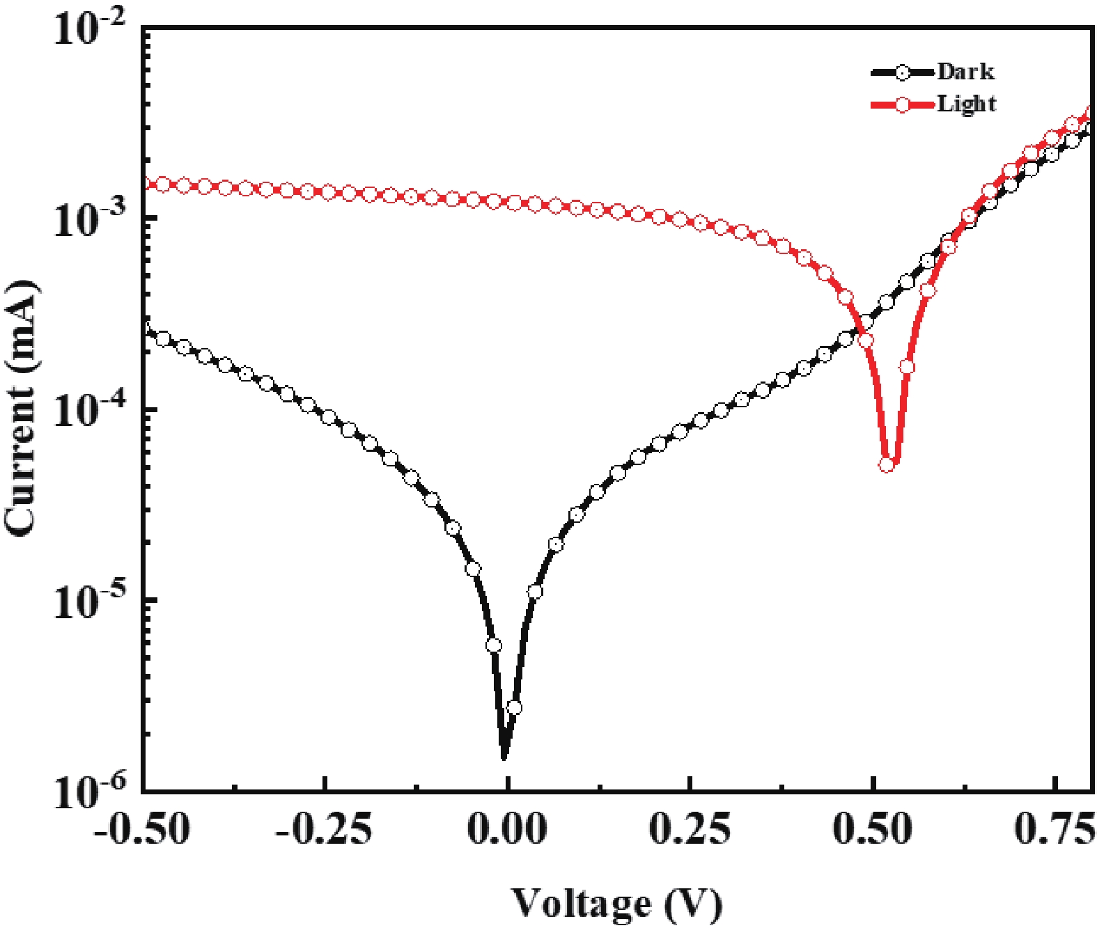
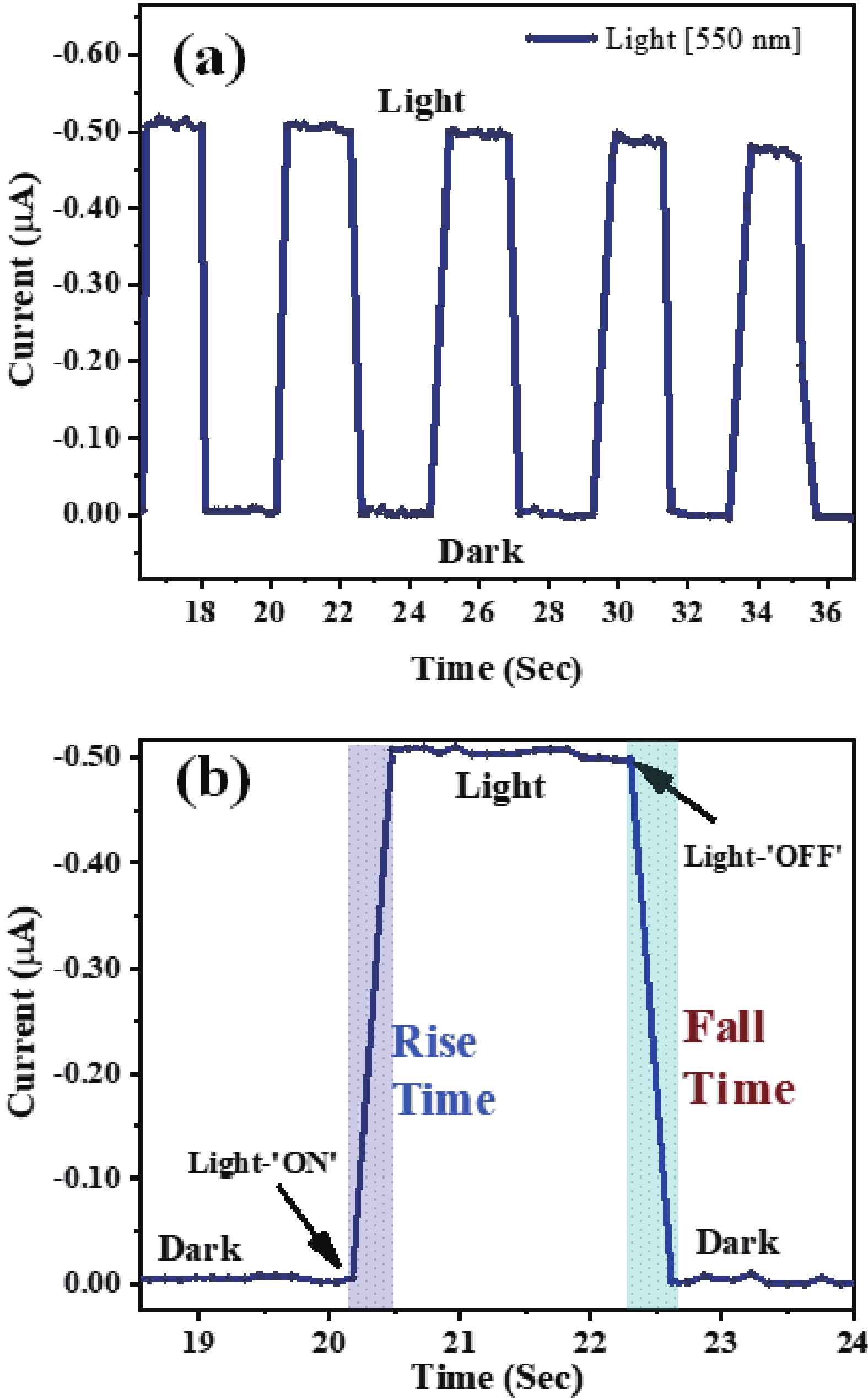
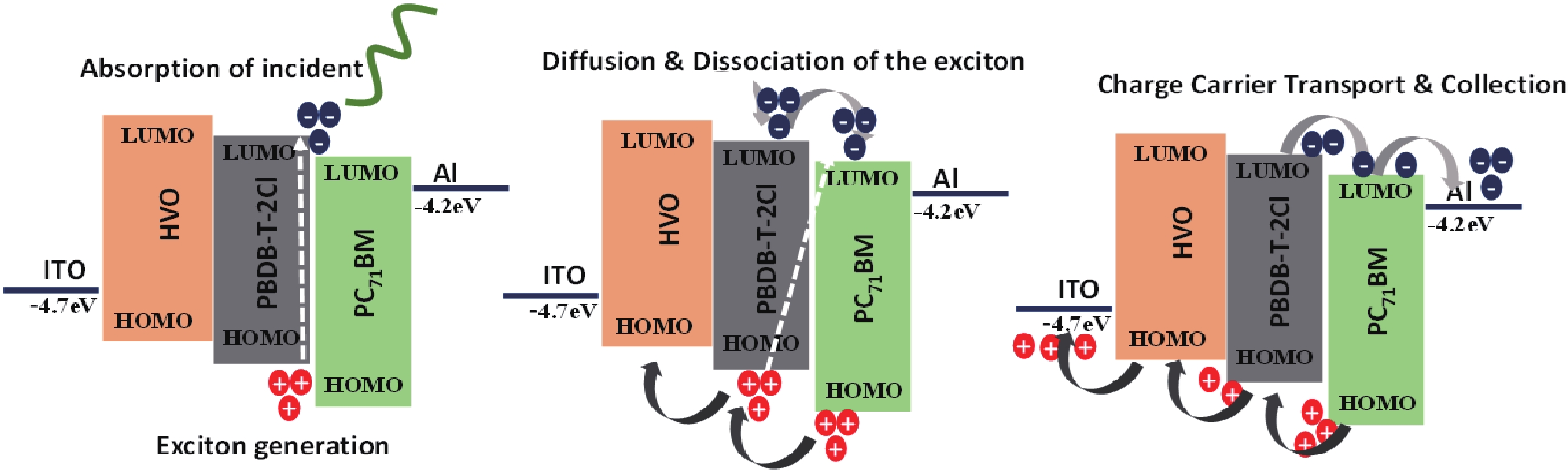
This article demonstrates the fabrication of organic-based devices using a low-cost solution-processable technique. A blended heterojunction of chlorine substituted 2D-conjugated polymer PBDB-T-2Cl, and PC71BM supported nanocapsules hydrate vanadium penta oxides (HVO) as hole transport layer (HTL) based photodetector fabricated on an ITO coated glass substrate under ambient condition. The device forms an excellent organic junction diode with a good rectification ratio of ~200. The device has also shown excellent photodetection properties under photoconductive mode (at reverse bias) and zero bias for green light wavelength. A very high responsivity of ~6500 mA/W and high external quantum efficiency (EQE) of 1400% have been reported in the article. The proposed organic photodetector exhibits an excellent response and recovery time of ~30 and ~40 ms, respectively.

J. Semicond.
2022, 43(9): 092401 doi: 10.1088/1674-4926/43/9/092401
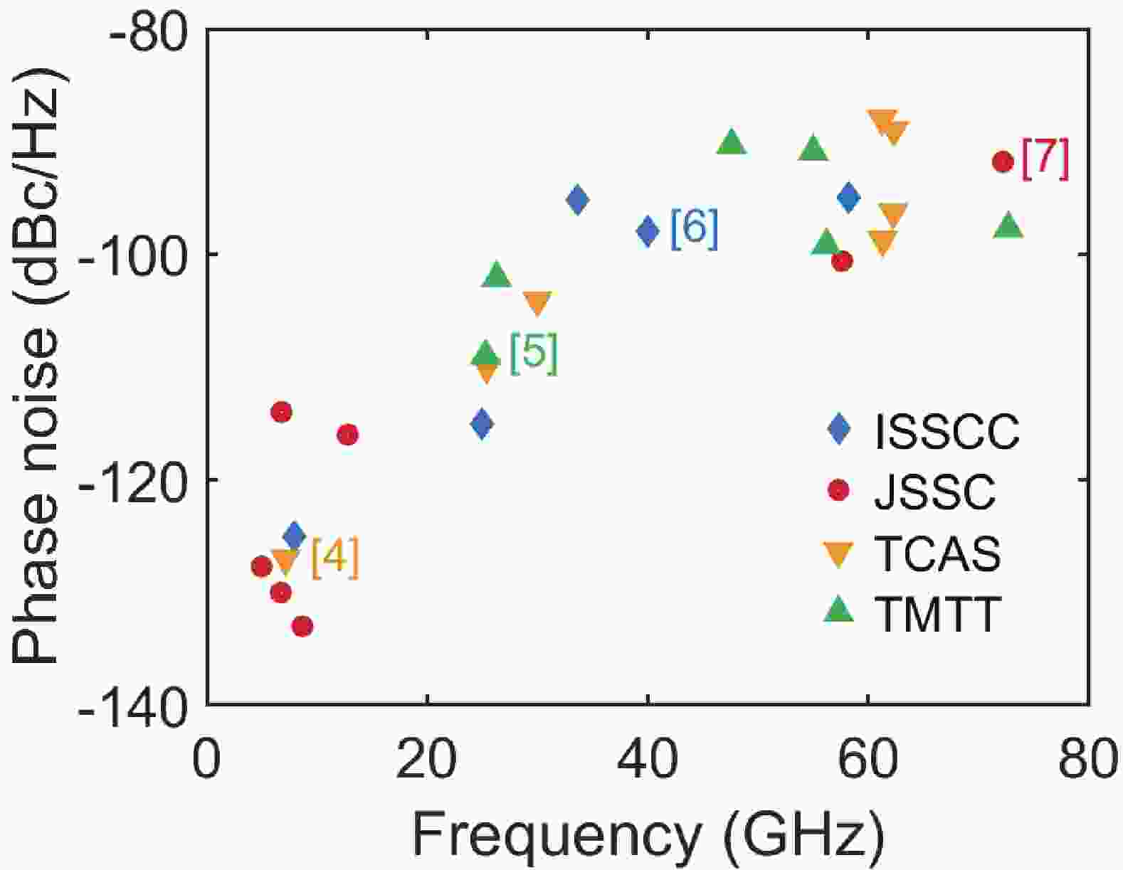
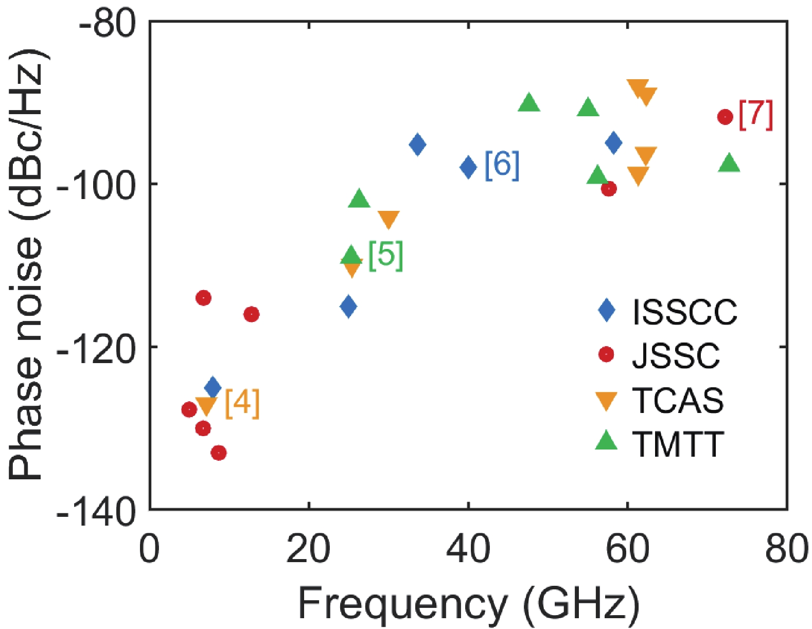
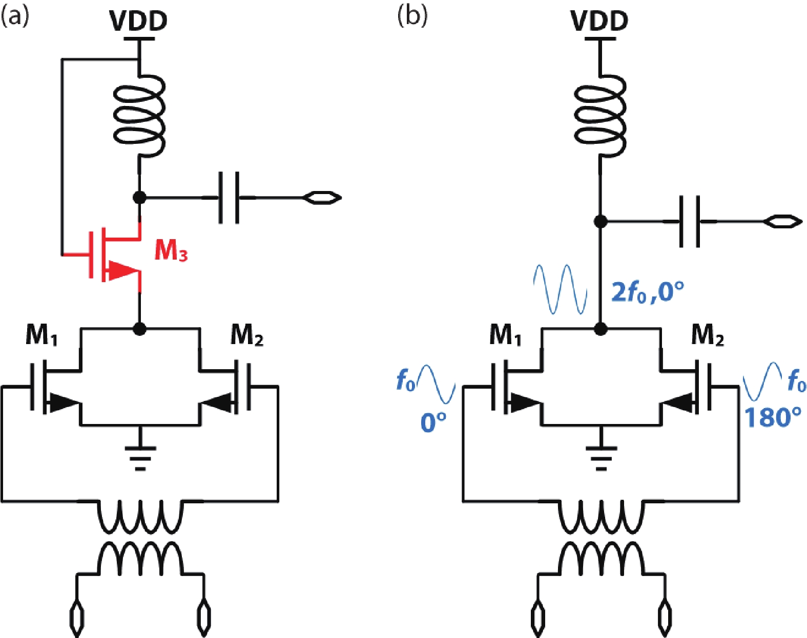
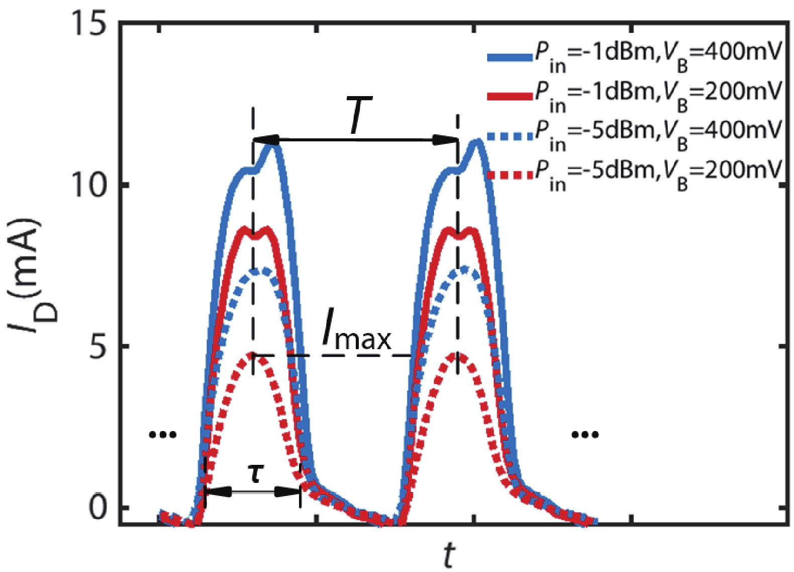
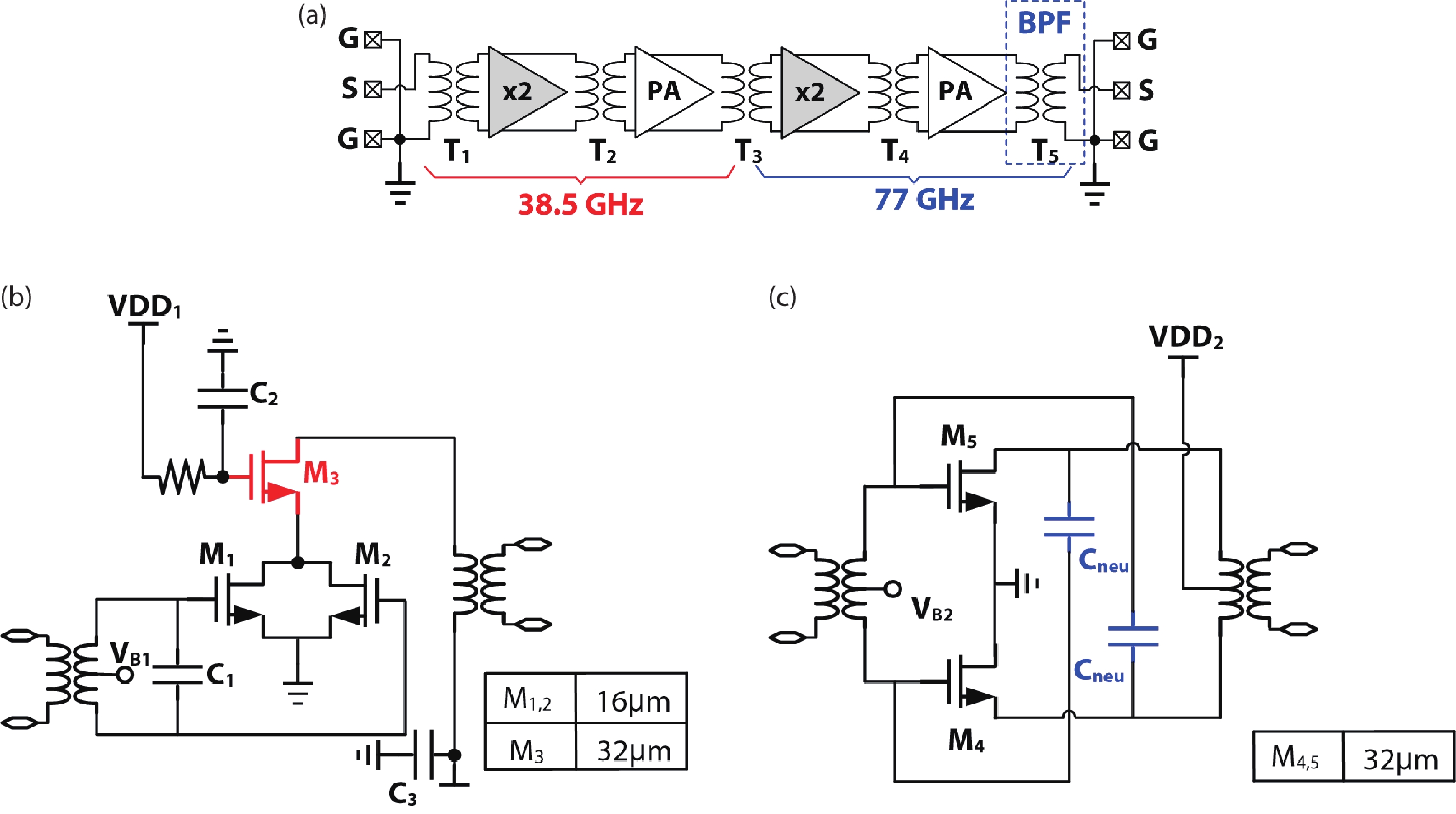
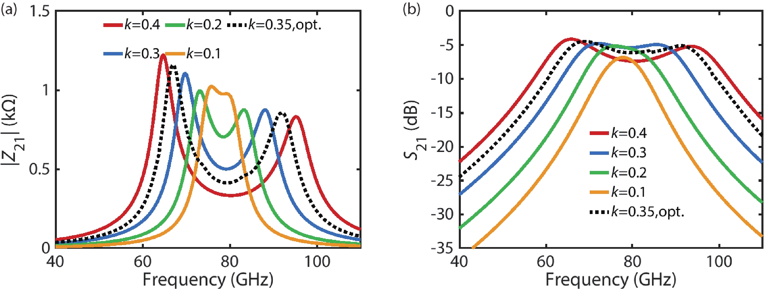
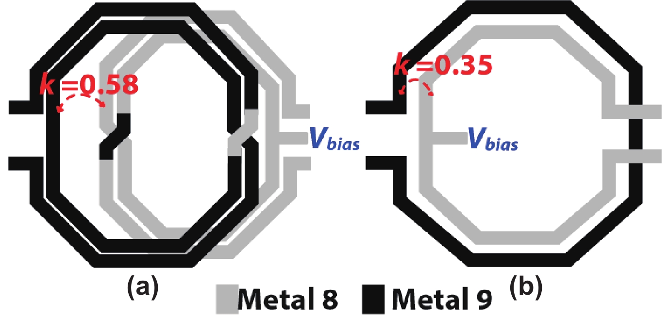
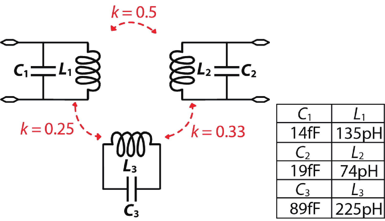
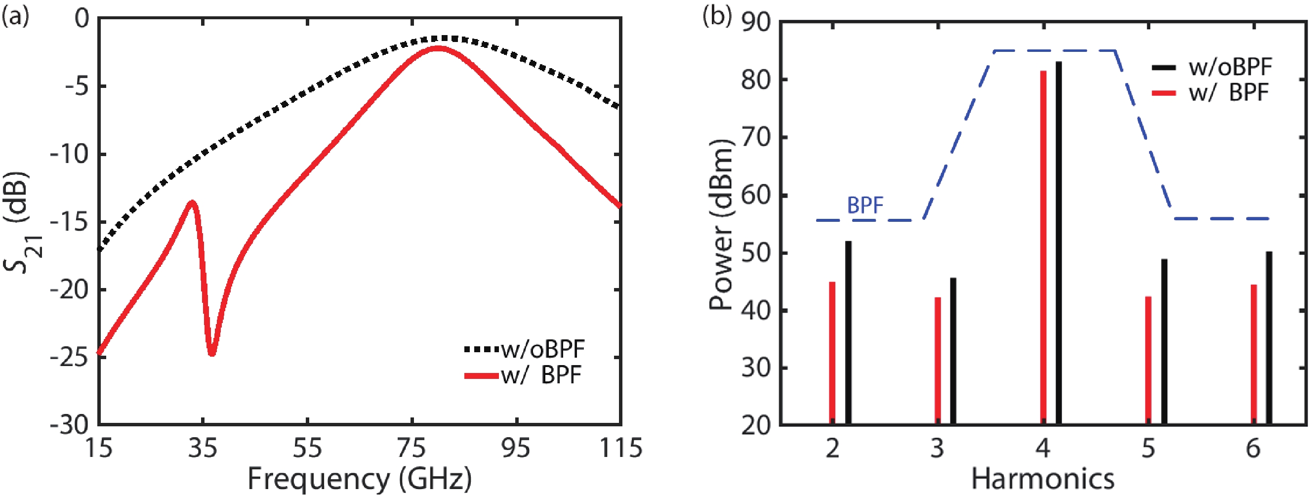
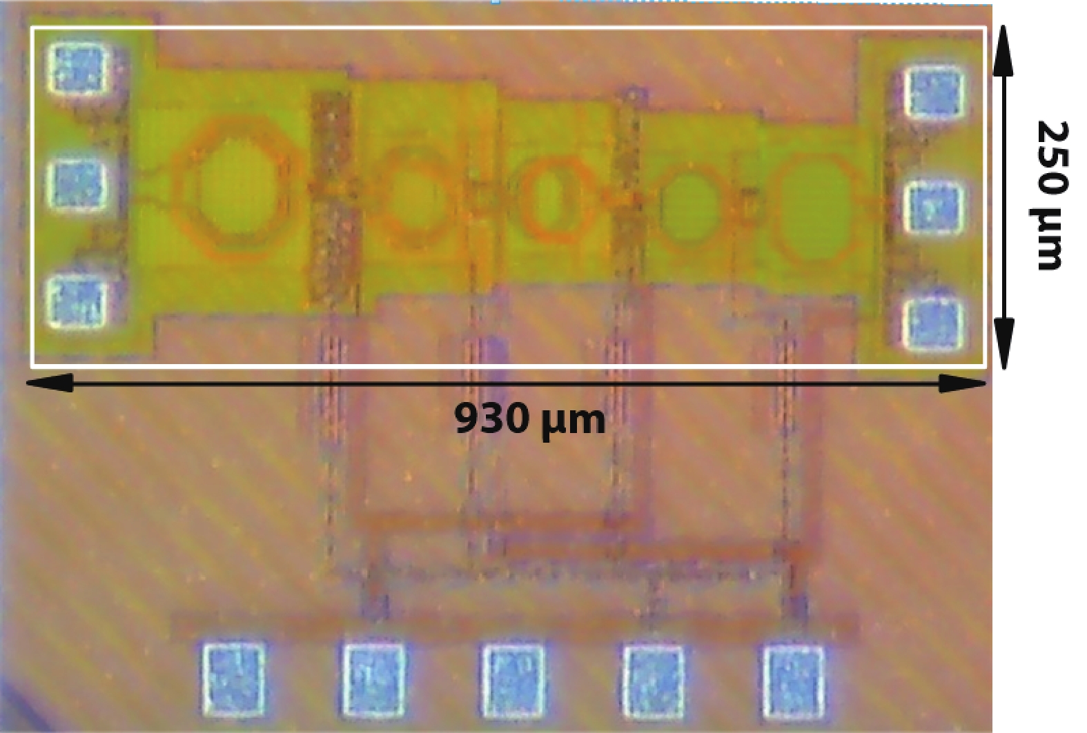
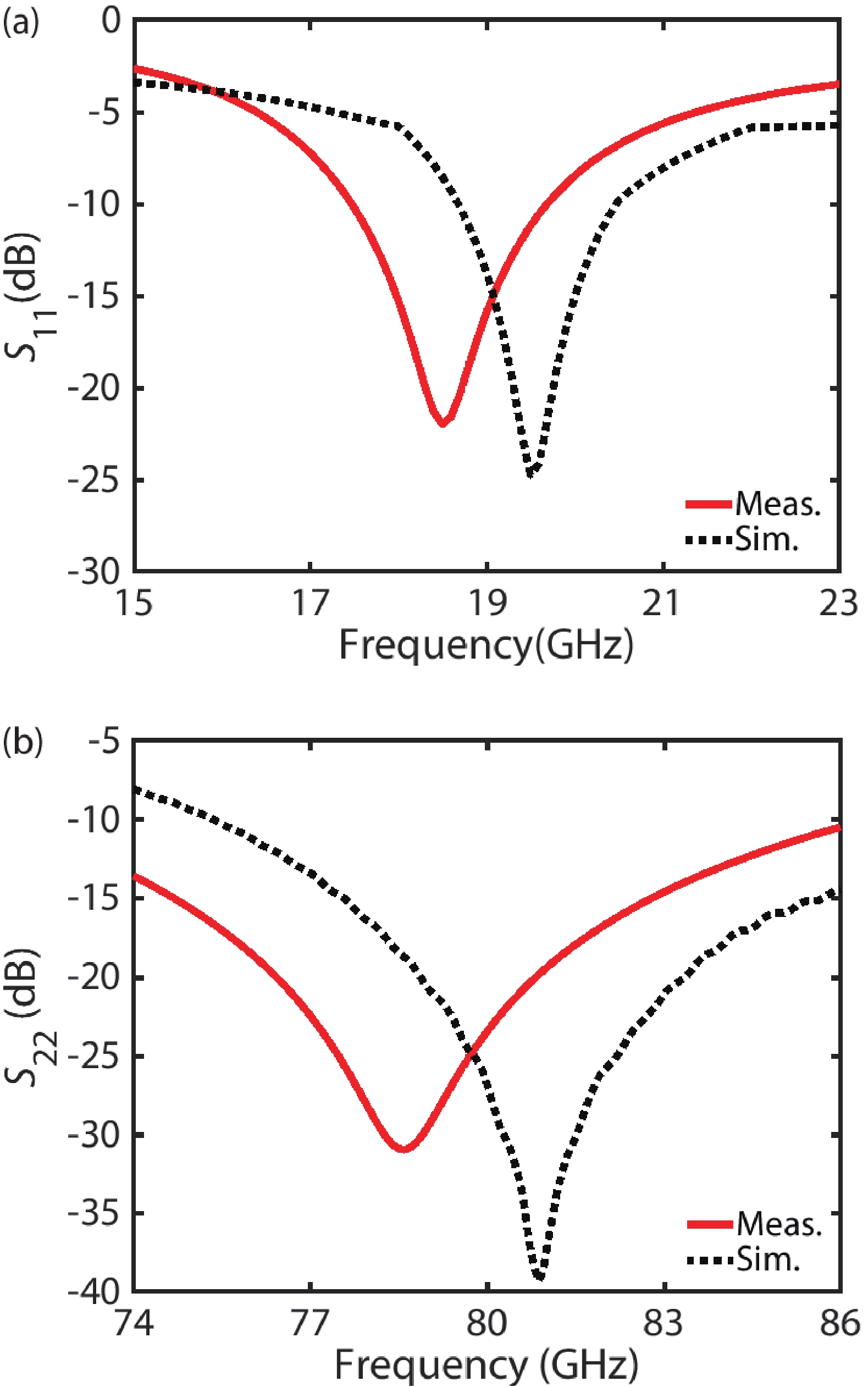
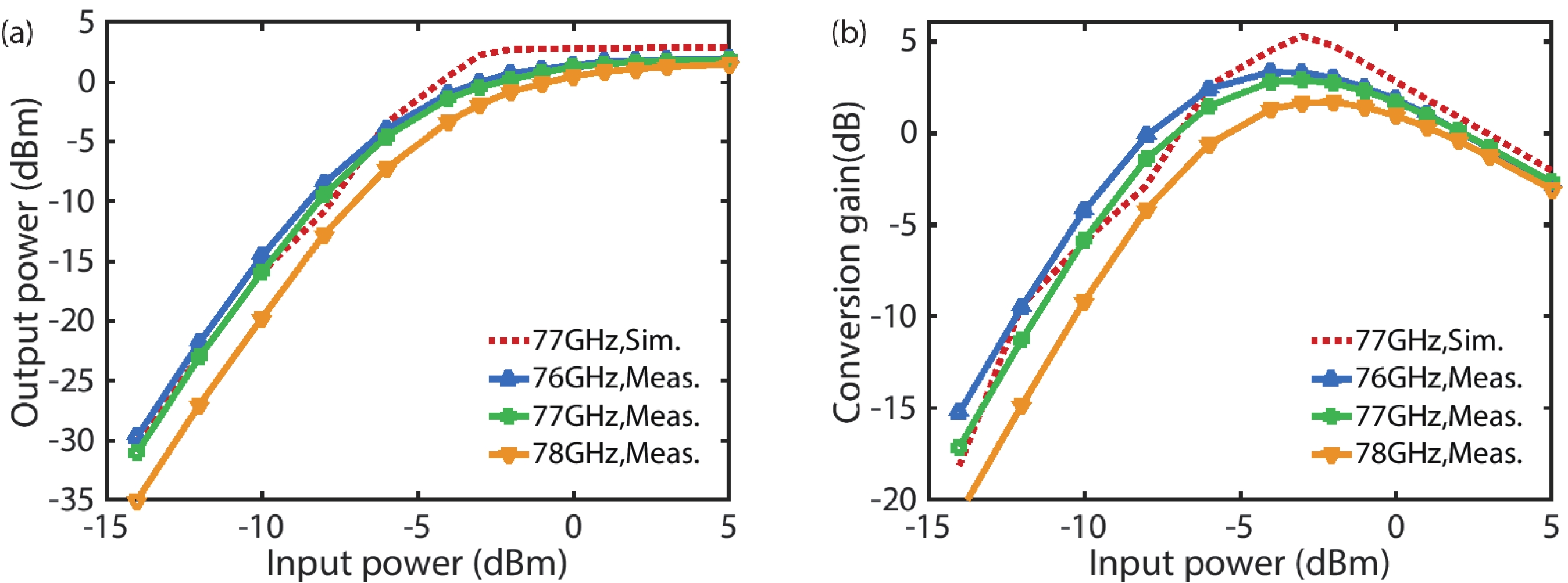
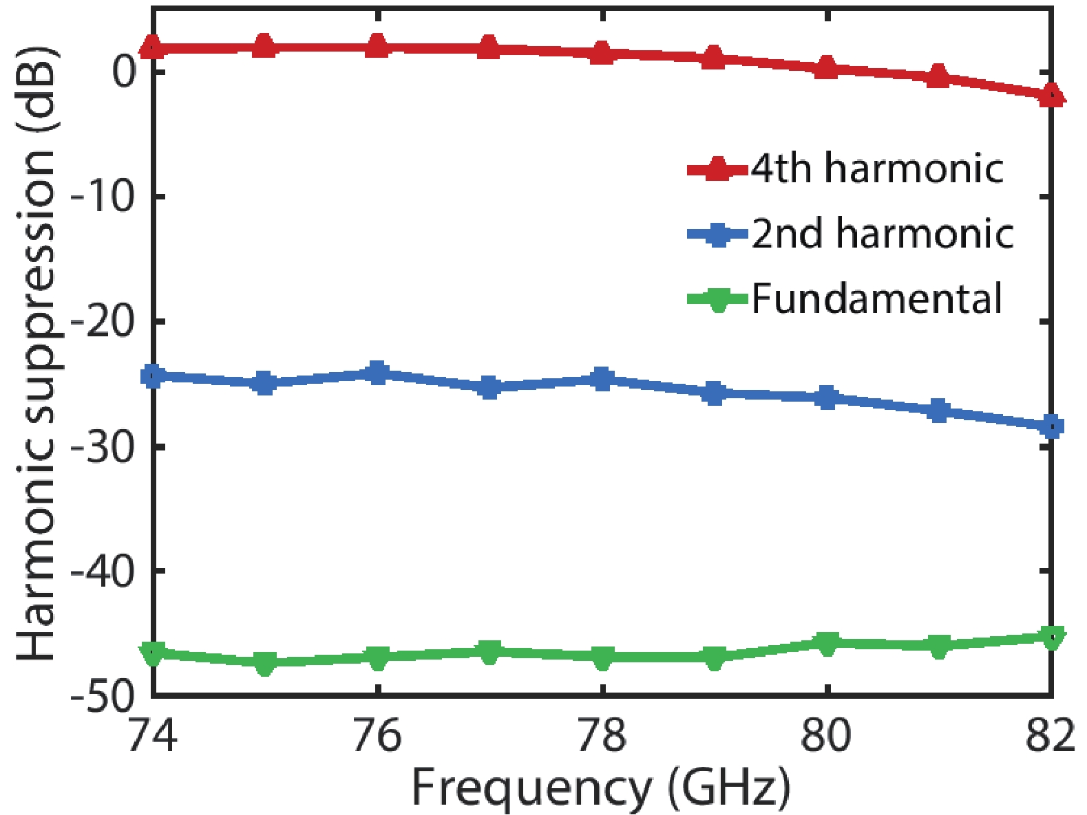
This paper presents an E-band frequency quadrupler in 40-nm CMOS technology. The circuit employs two push–push frequency doublers and two single-stage neutralized amplifiers. The pseudo-differential class-B biased cascode topology is adopted for the frequency doubler, which improves the reverse isolation and the conversion gain. Neutralization technique is applied to increase the stability and the power gain of the amplifiers simultaneously. The stacked transformers are used for single-ended-to-differential transformation as well as output bandpass filtering. The output bandpass filter enhances the 4th-harmonic output power, while rejecting the undesired harmonics, especially the 2nd harmonic. The core chip is 0.23 mm2 in size and consumes 34 mW. The measured 4th harmonic achieves a maximum output power of 1.7 dBm with a peak conversion gain of 3.4 dB at 76 GHz. The fundamental and 2nd-harmonic suppressions of over 45 and 20 dB are achieved for the spectrum from 74 to 82 GHz, respectively.


J. Semicond.
2022, 43(9): 092501 doi: 10.1088/1674-4926/43/9/092501
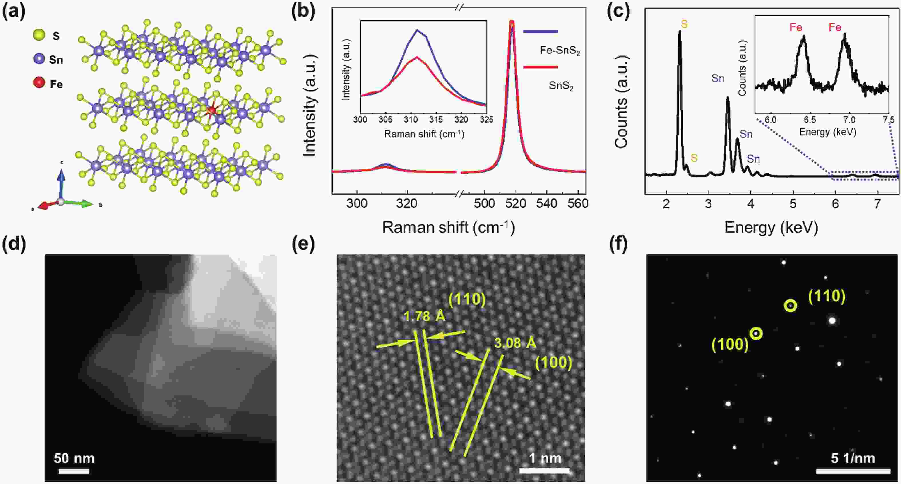
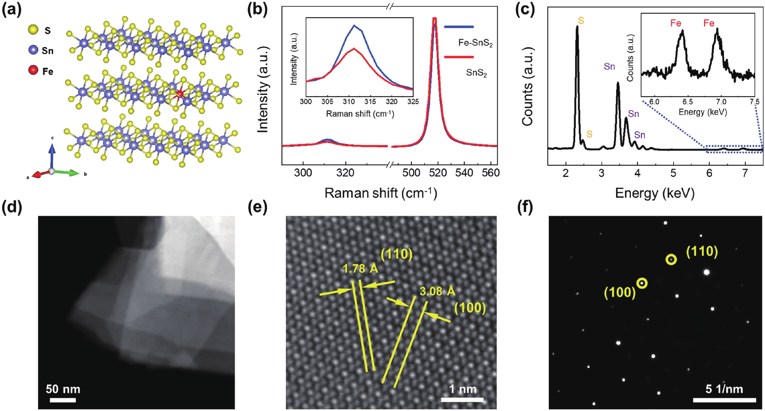
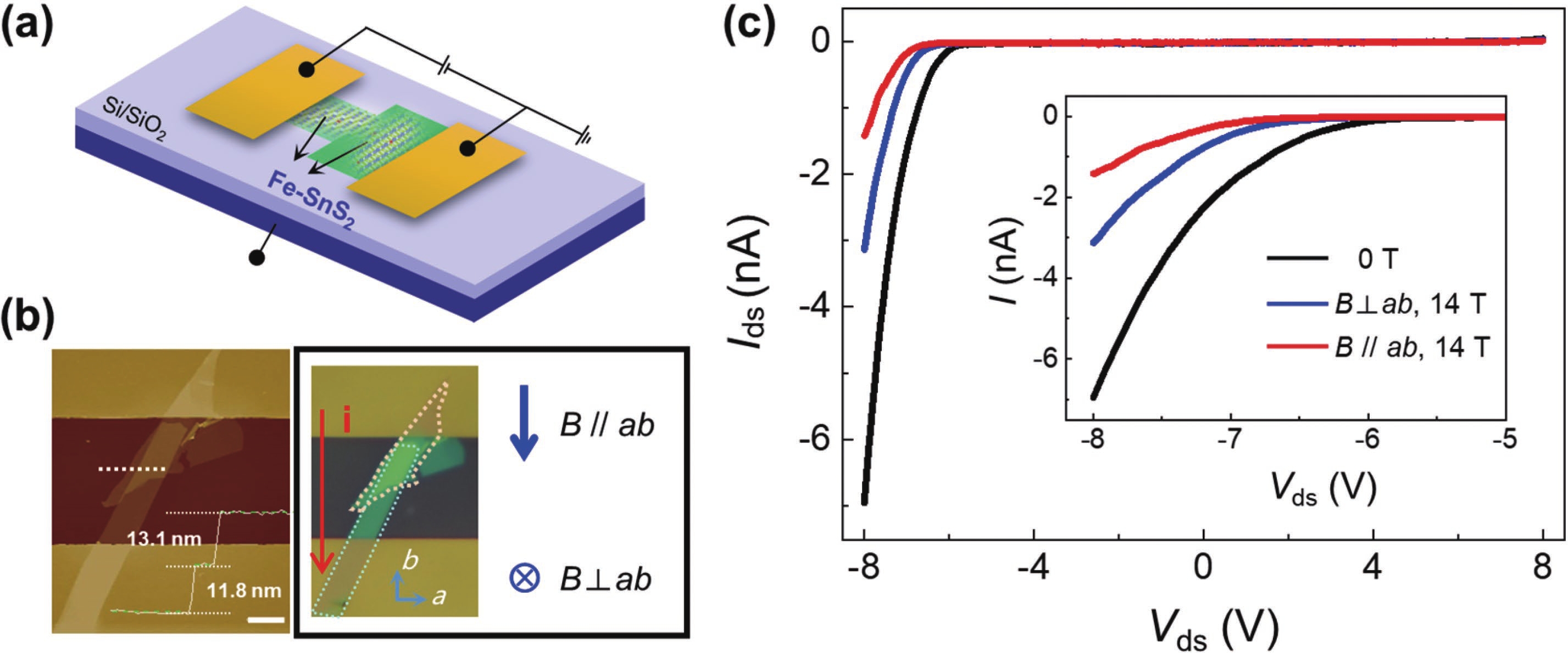
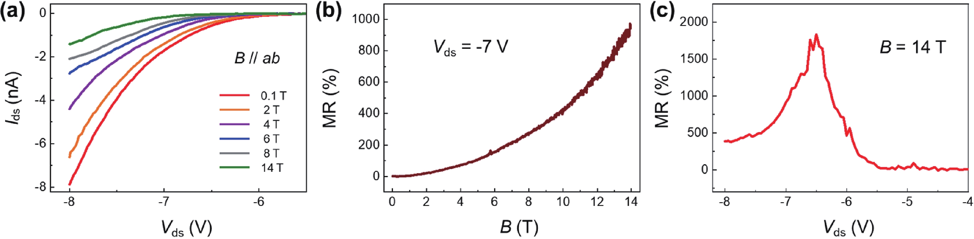
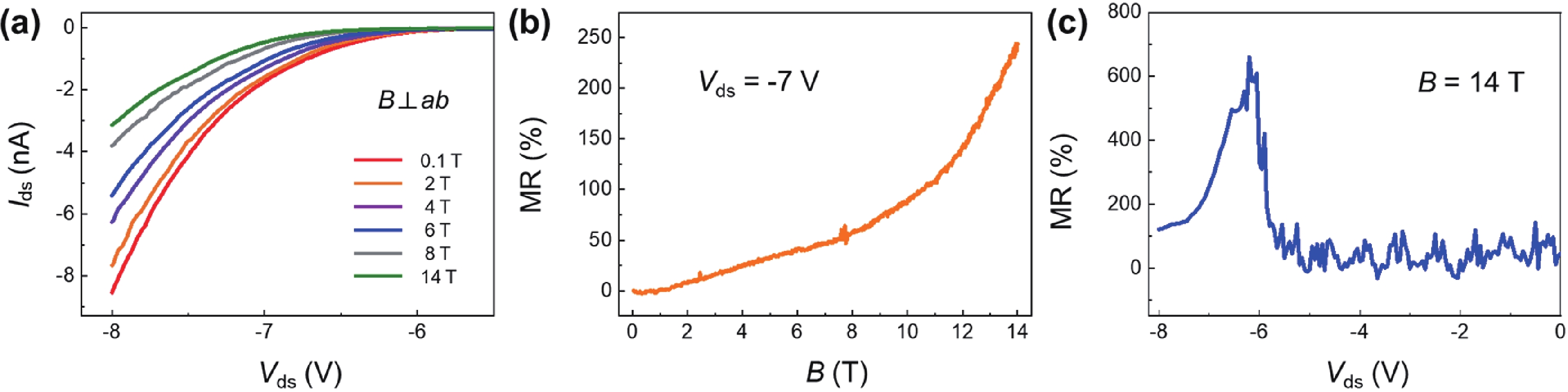
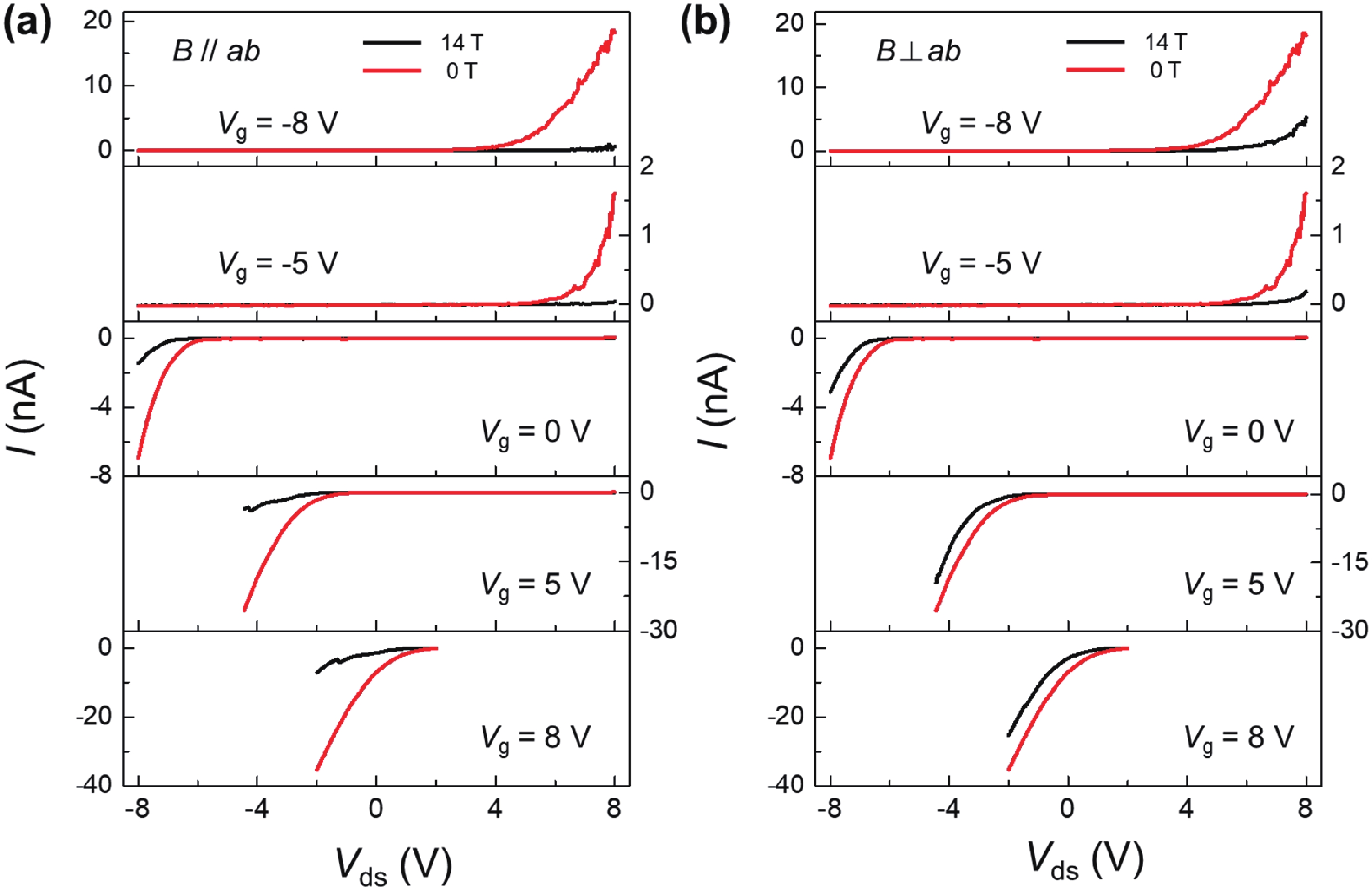
A magnetic semiconductor whose electronic charge and spin can be regulated together will be an important component of future spintronic devices. Here, we construct a two-dimensional (2D) Fe doped SnS2 (Fe-SnS2) homogeneous junction and investigate its electromagnetic transport feature. The Fe-SnS2 homojunction device showed large positive and unsaturated magnetoresistance (MR) of 1800% in the parallel magnetic field and 600% in the vertical magnetic field, indicating an obvious anisotropic MR feature. In contrast, The MR of Fe-SnS2 homojunction is much larger than the pure diamagnetic SnS2 and most 2D materials. The application of a gate voltage can regulate the MR effect of Fe-SnS2 homojunction devices. Moreover, the stability of Fe-SnS2 in air has great application potential. Our Fe-SnS2 homojunction has a significant potential in future magnetic memory applications.
J. Semicond.
2022, 43(9): 092601 doi: 10.1088/1674-4926/43/9/092601
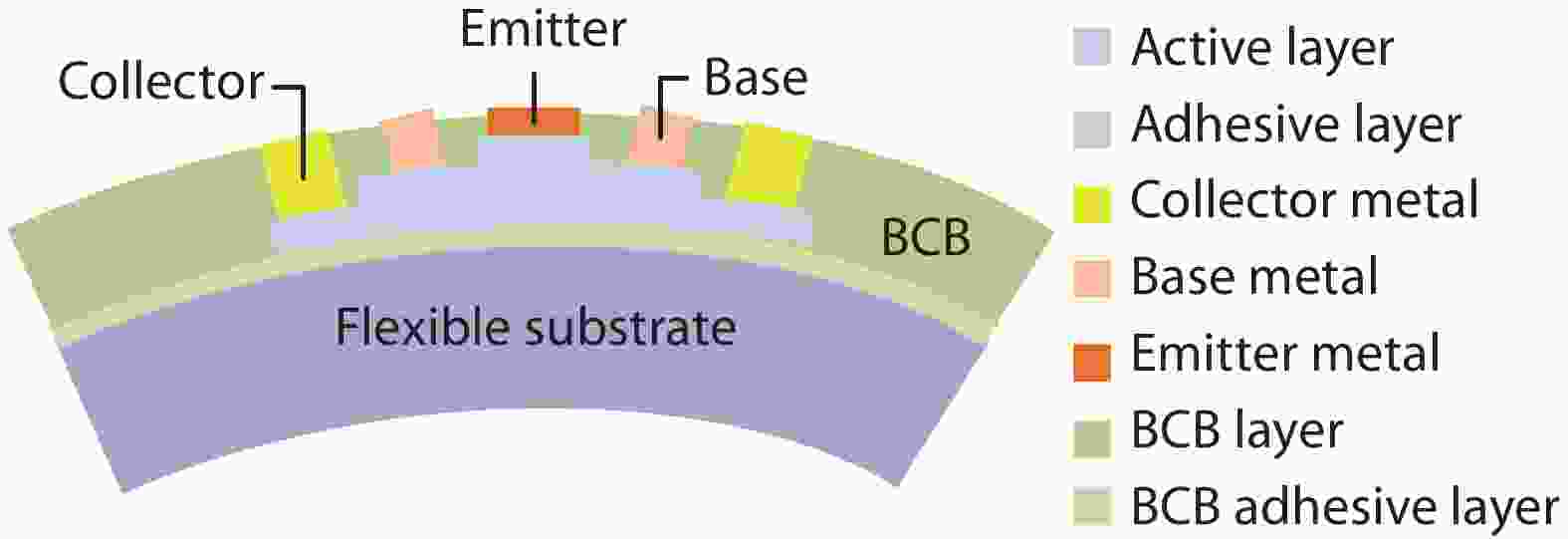
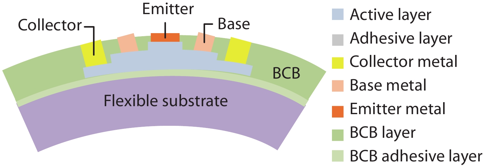
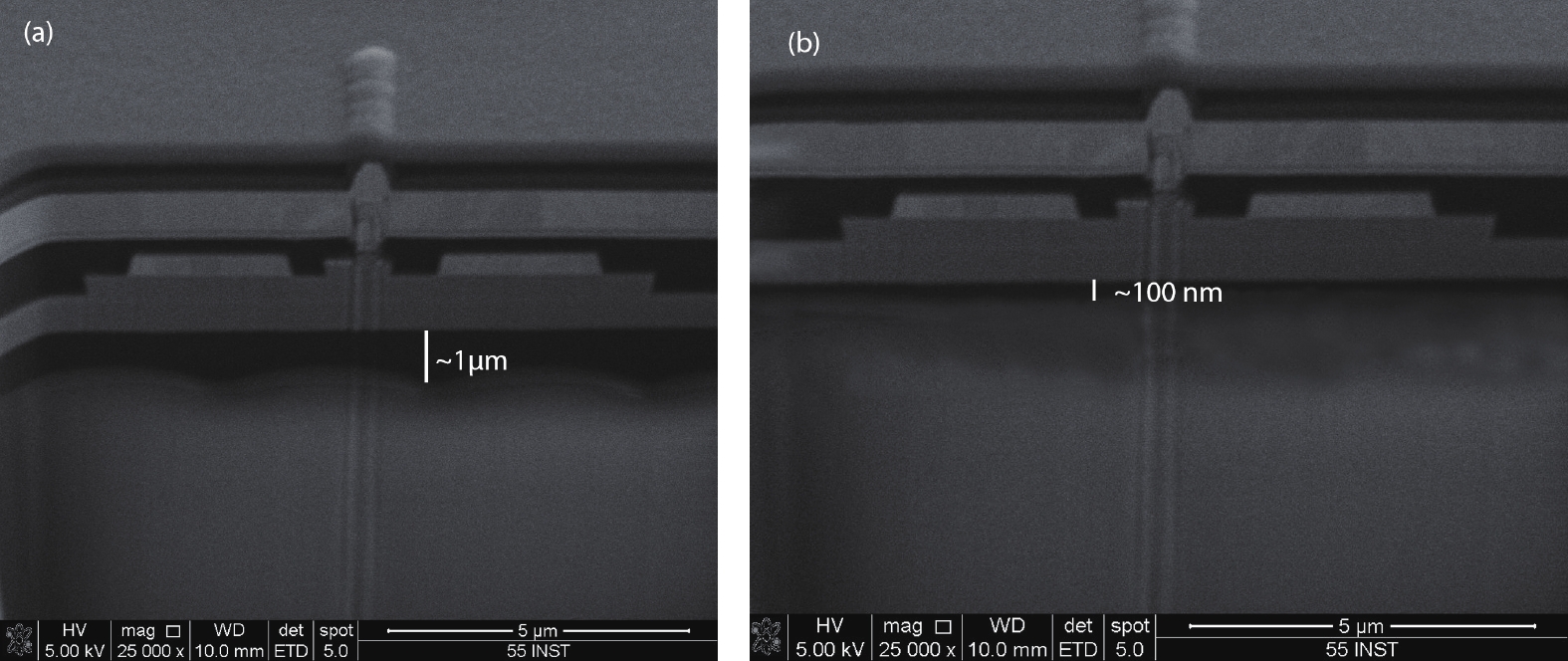
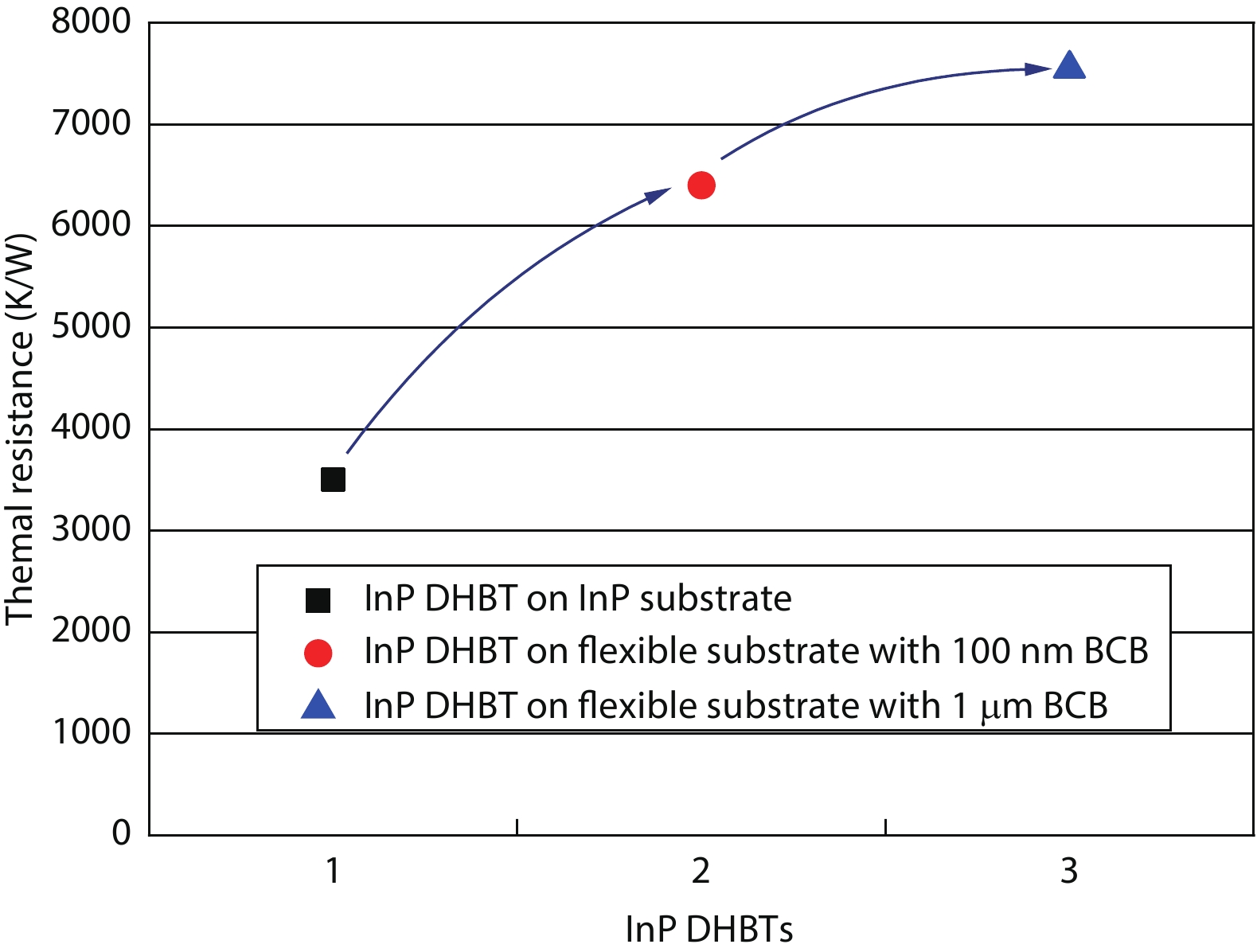
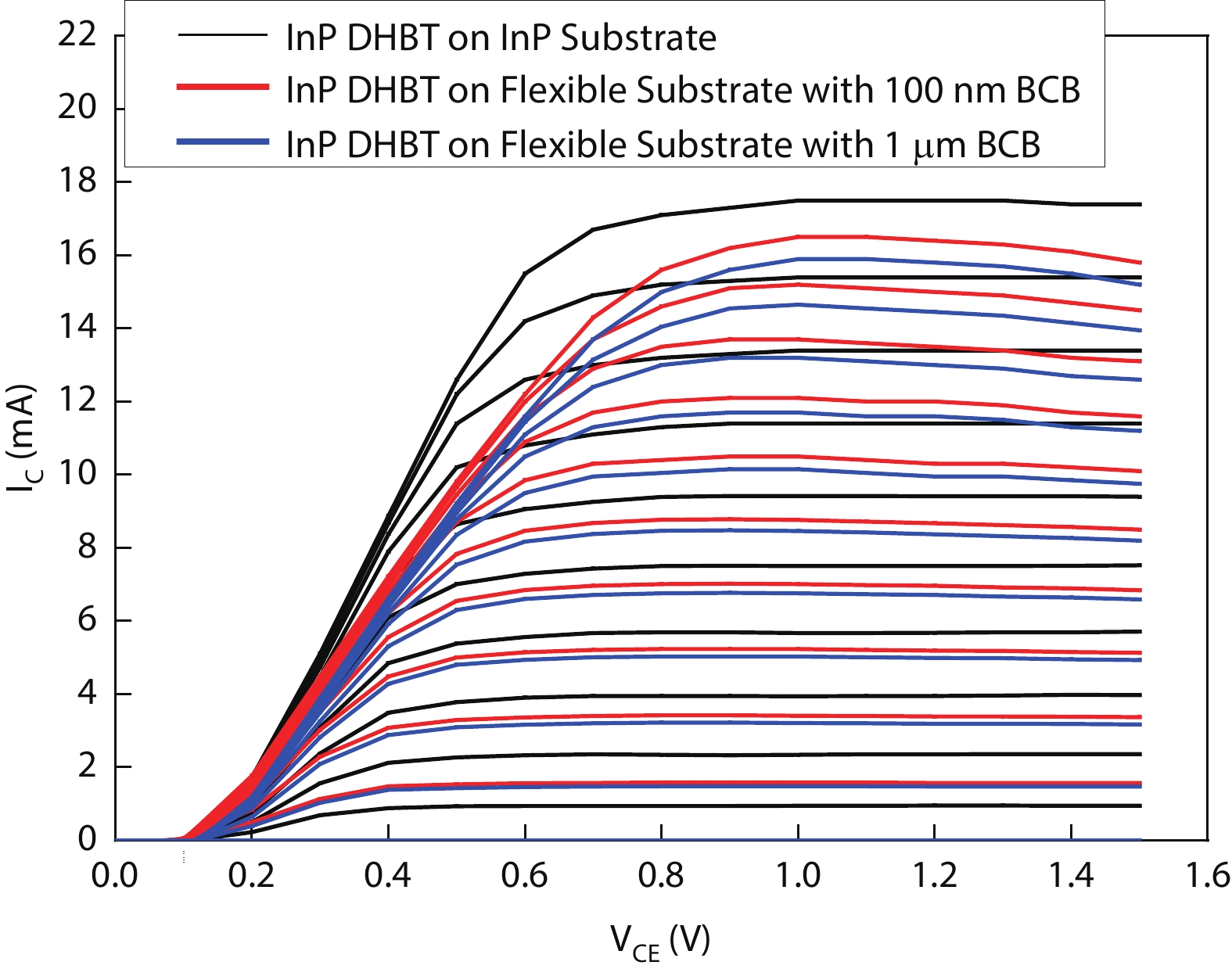
This letter presents the fabrication of InP double heterojunction bipolar transistors (DHBTs) on a 3-inch flexible substrate with various thickness values of the benzocyclobutene (BCB) adhesive bonding layer, the corresponding thermal resistance of the InP DHBT on flexible substrate is also measured and calculated. InP DHBT on a flexible substrate with 100 nm BCB obtains cut-off frequency fT = 358 GHz and maximum oscillation frequency fMAX = 530 GHz. Moreover, the frequency performance of the InP DHBT on flexible substrates at different bending radii are compared. It is shown that the bending strain has little effect on the frequency characteristics (less than 8.5%), and these bending tests prove that InP DHBT has feasible flexibility.


J. Semicond.
2022, 43(9): 092801 doi: 10.1088/1674-4926/43/9/092801

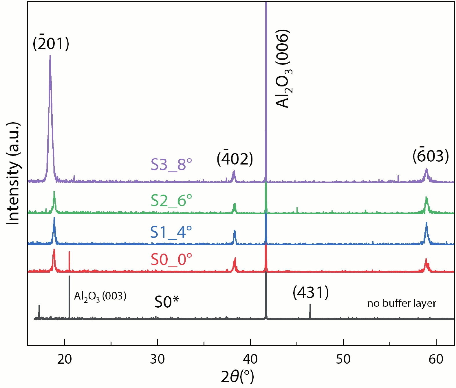
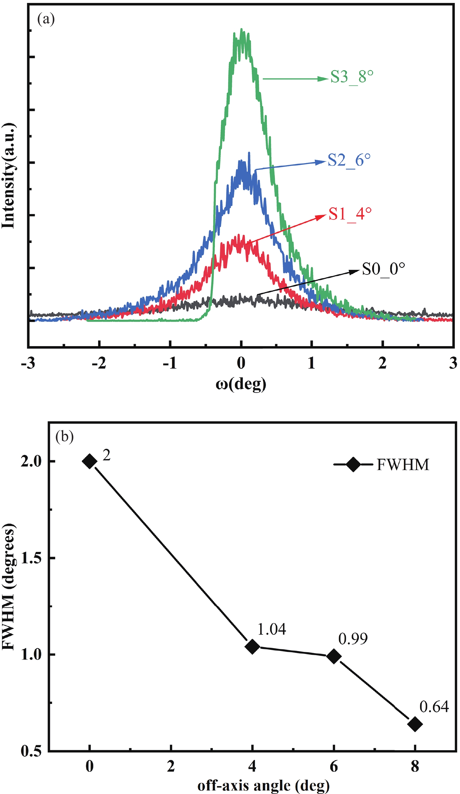
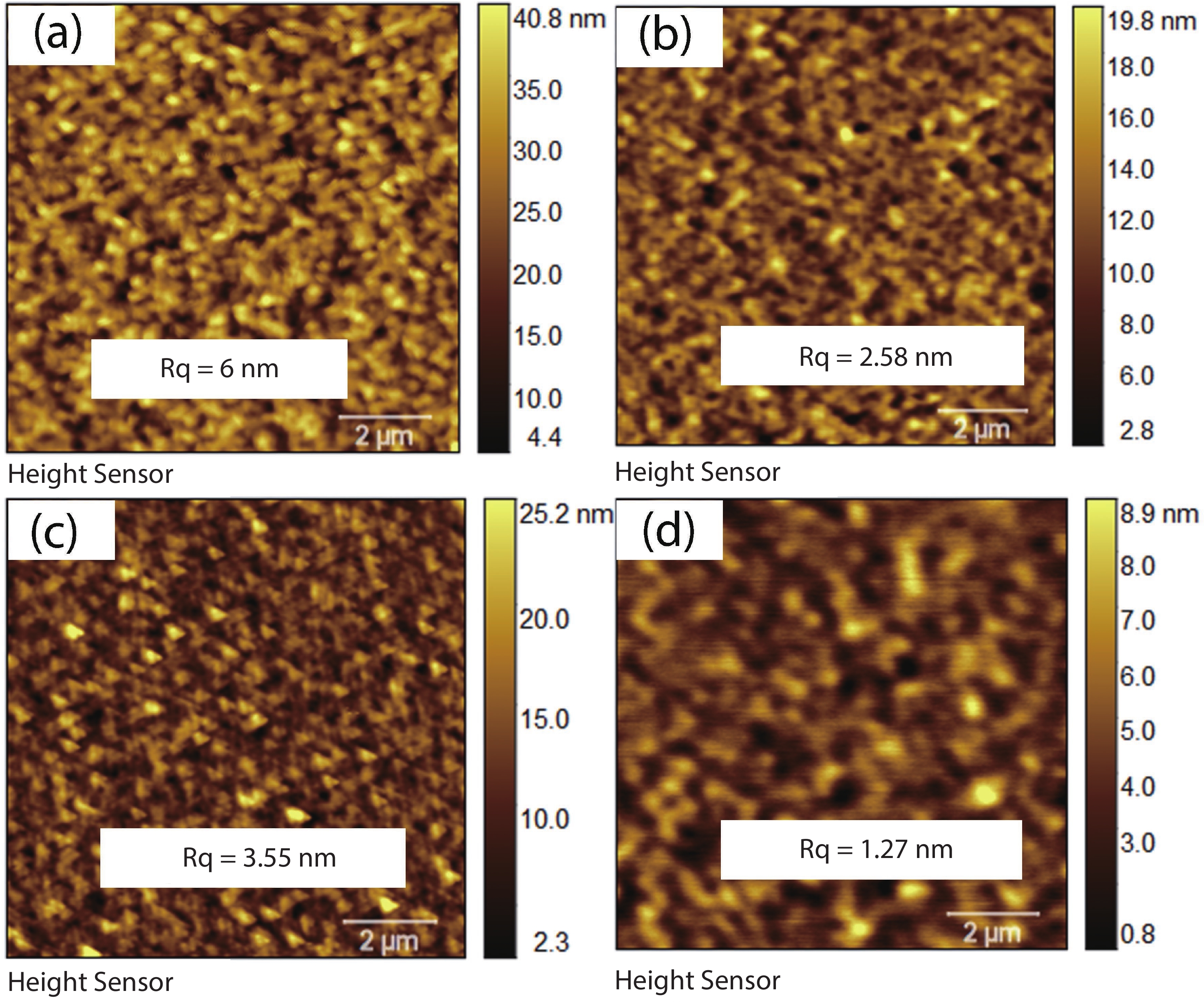
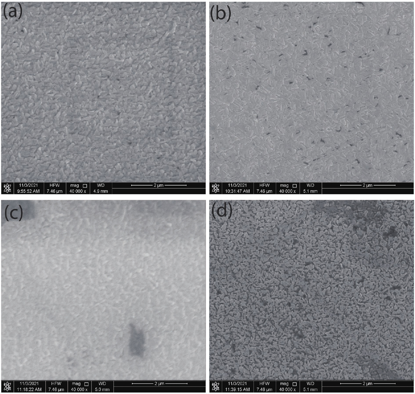
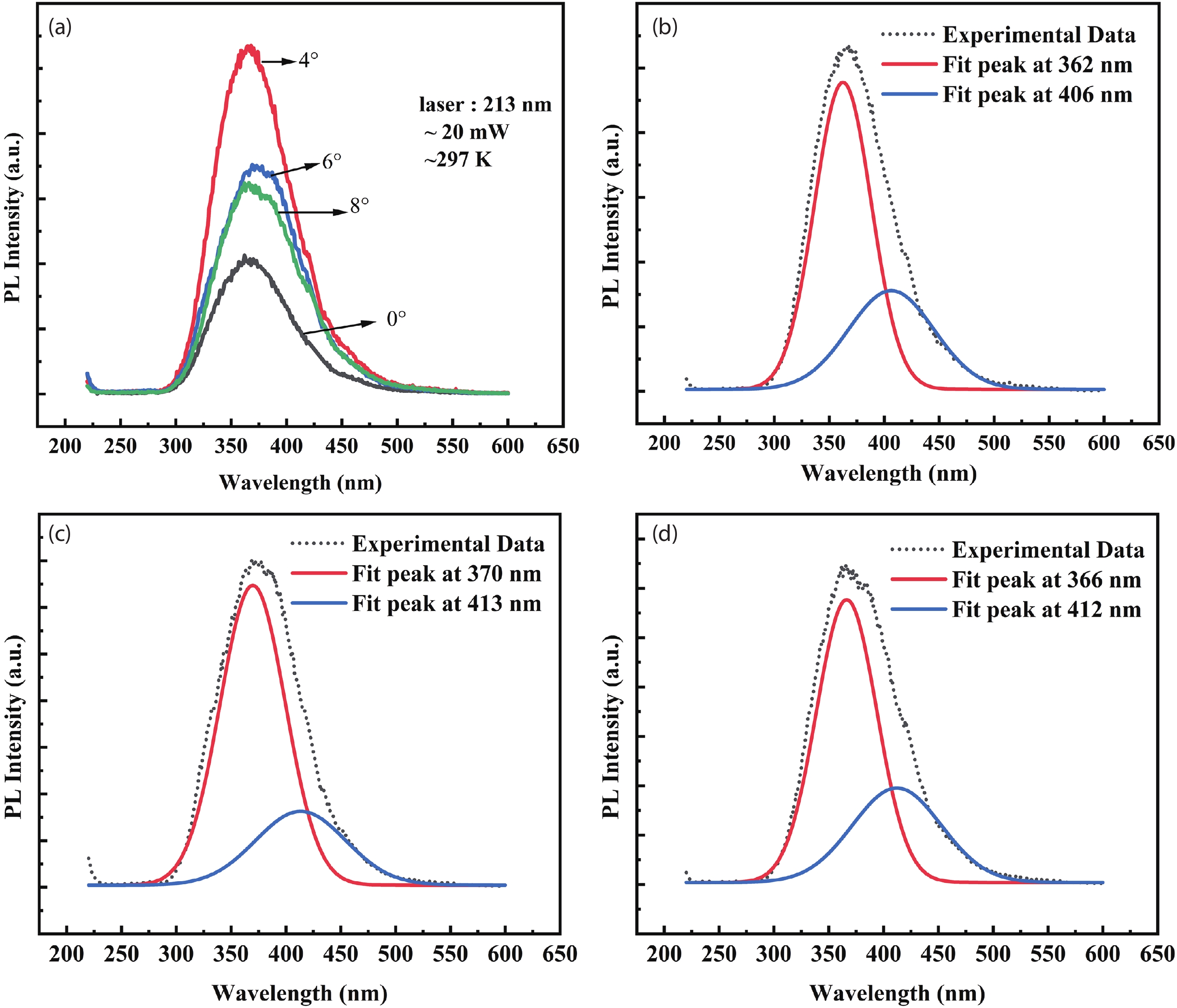
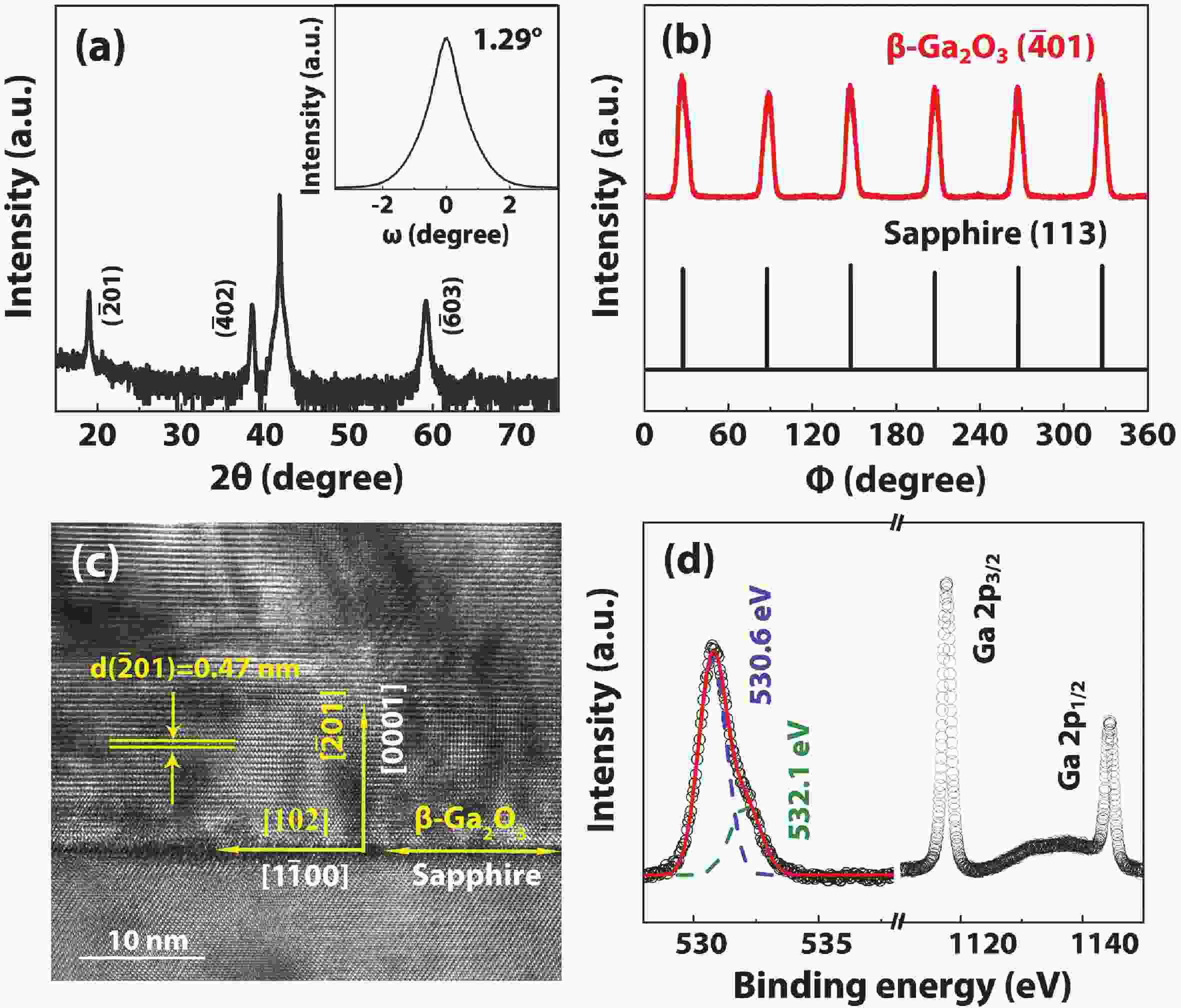
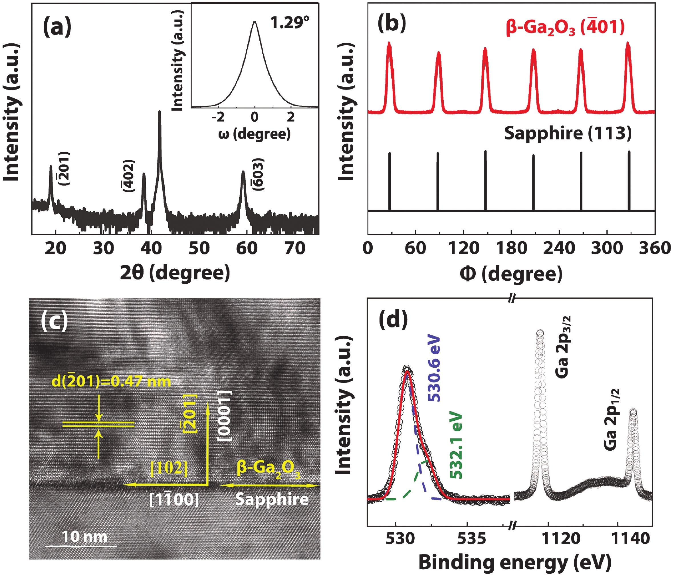
Beta-gallium oxide (β-Ga2O3) thin films were deposited on c-plane (0001) sapphire substrates with different mis-cut angles along <


J. Semicond.
2022, 43(9): 092802 doi: 10.1088/1674-4926/43/9/092802
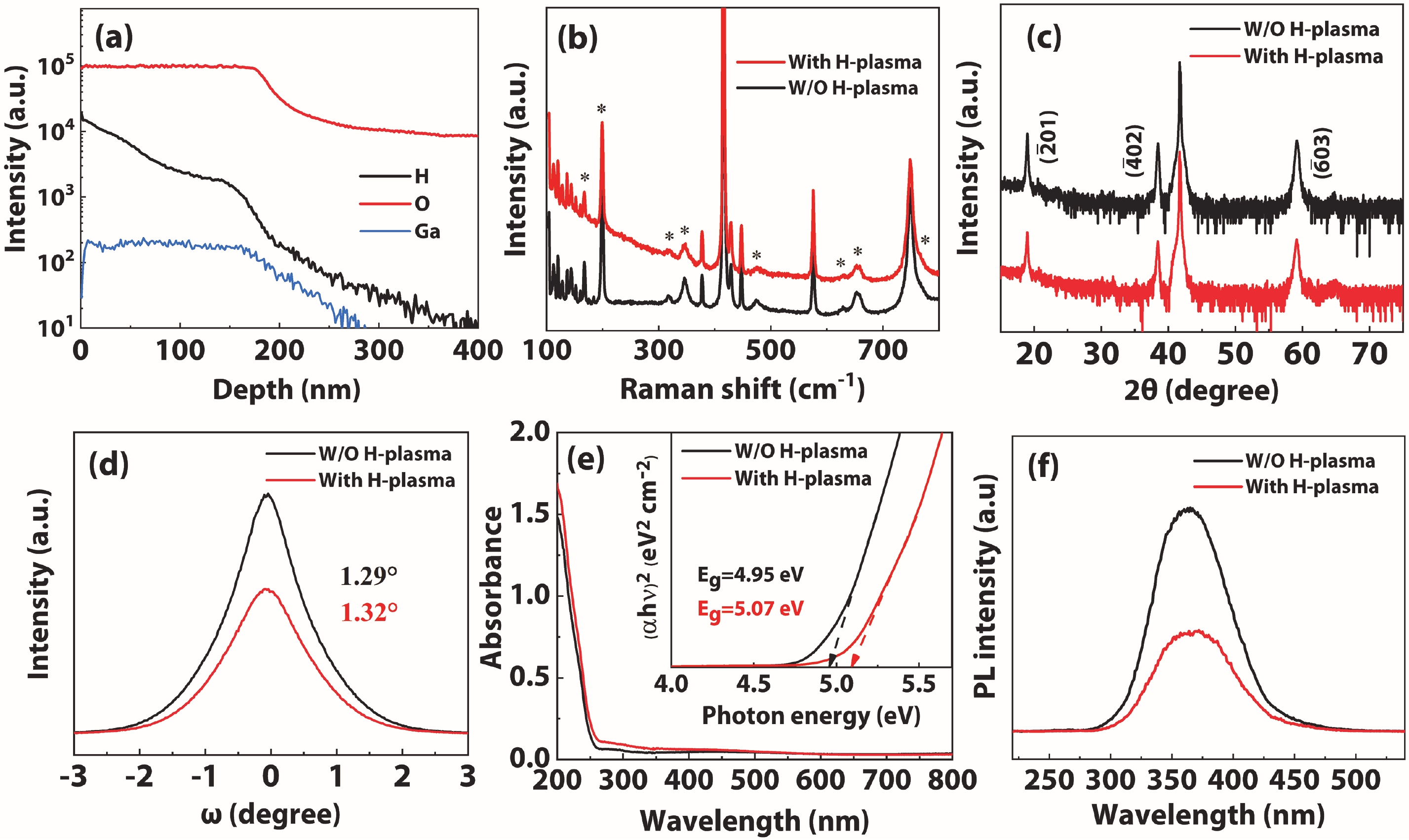
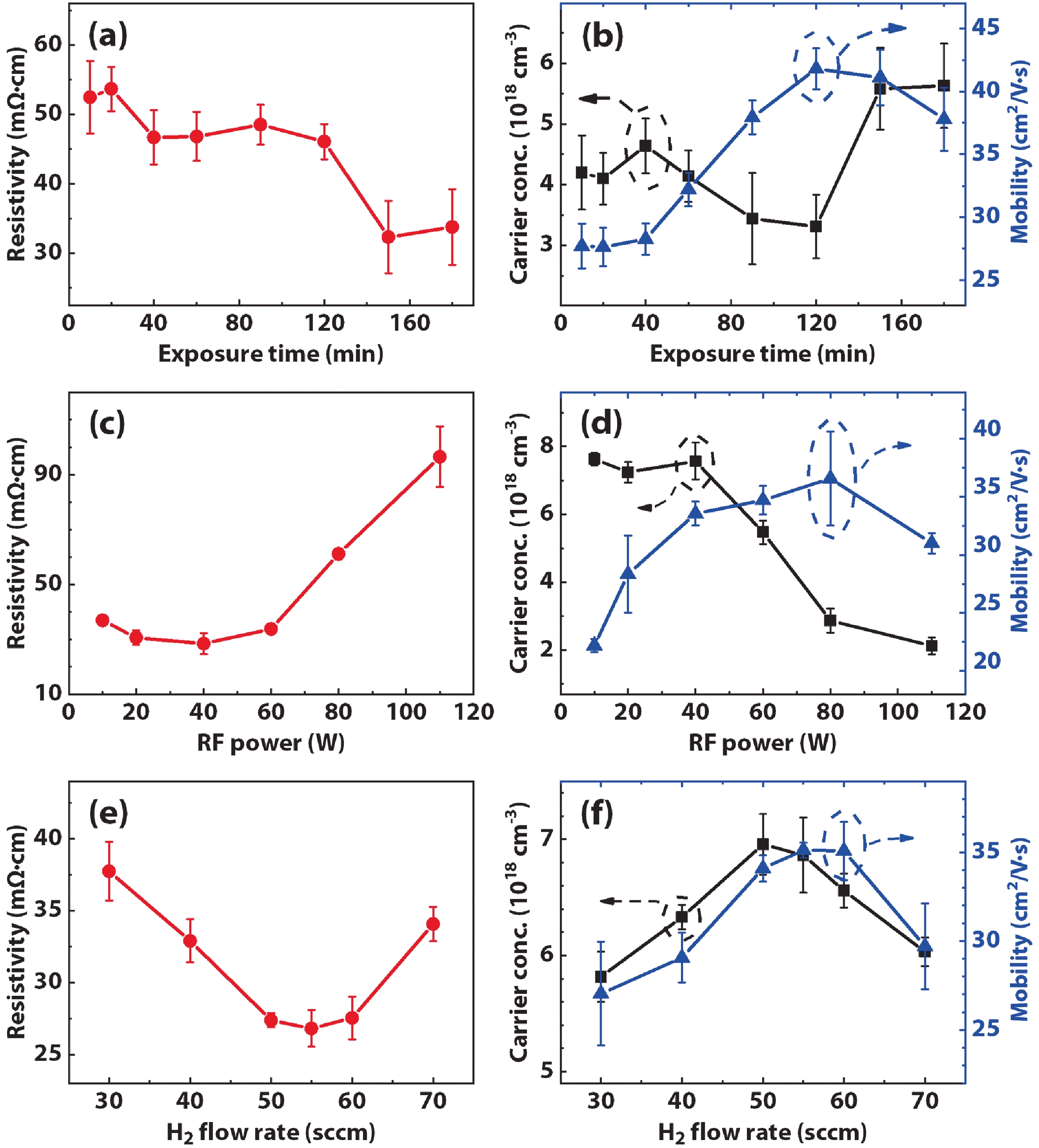
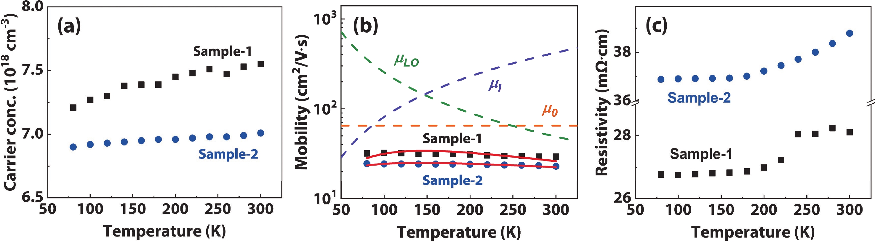
The behavior of H in β-Ga2O3 is of substantial interest because it is a common residual impurity that is present in β-Ga2O3, regardless of the synthesis methods. Herein, we report the influences of H-plasma exposure on the electric and optical properties of the heteroepitaxial β-Ga2O3 thin films grown on sapphire substrates by chemical vapor deposition. The results indicate that the H incorporation leads to a significantly increased electrical conductivity, a greatly reduced defect-related photoluminescence emission, and a slightly enhanced transmittance, while it has little effect on the crystalline quality of the β-Ga2O3 films. The significant changes in the electrical and optical properties of β-Ga2O3 may originate from the formation of shallow donor states and the passivation of the defects by the incorporated H. Temperature dependent electrical properties of the H-incorporated β-Ga2O3 films are also investigated, and the dominant scattering mechanisms at various temperatures are discussed.
J. Semicond.
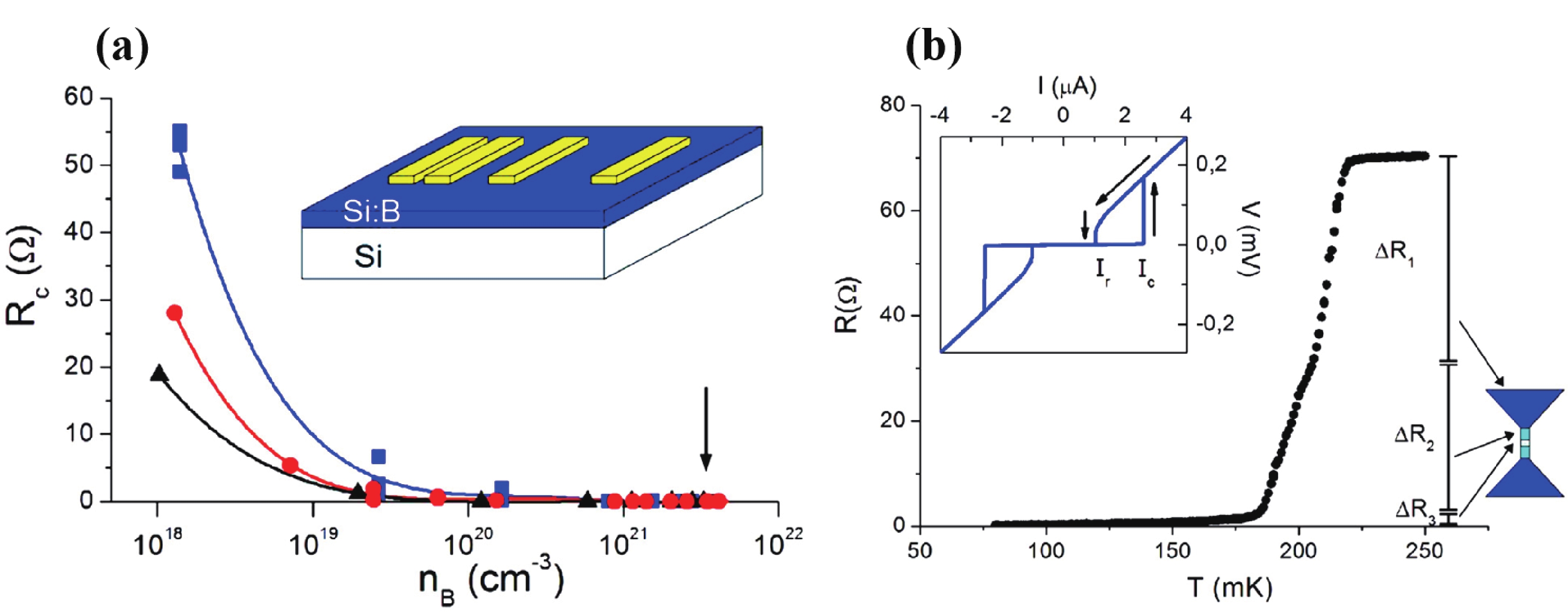
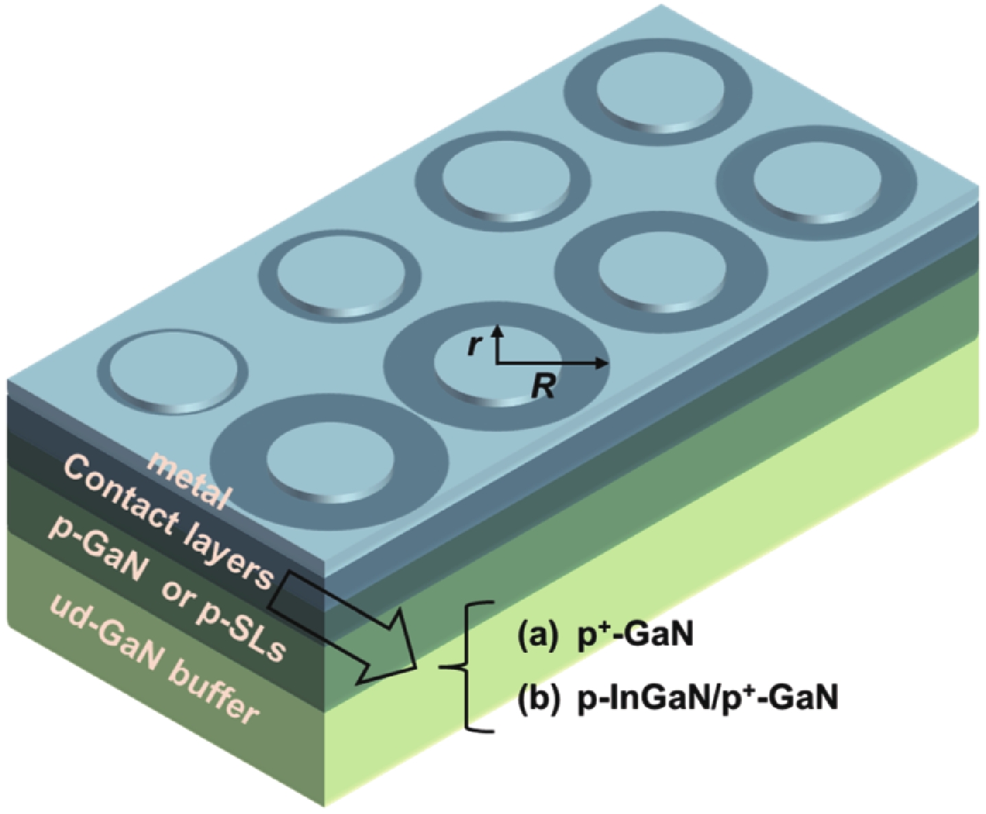
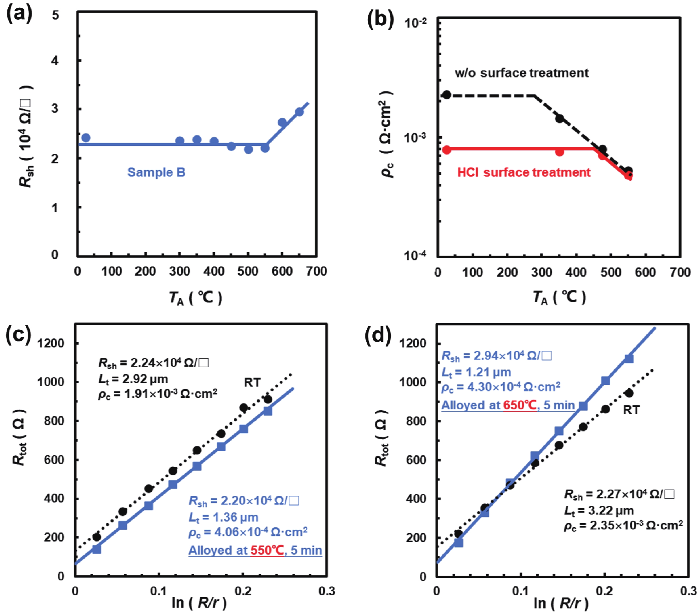
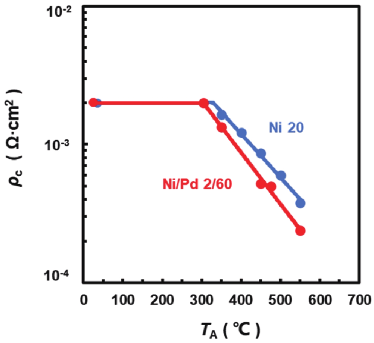
2022, 43(9): 092803 doi: 10.1088/1674-4926/43/9/092803
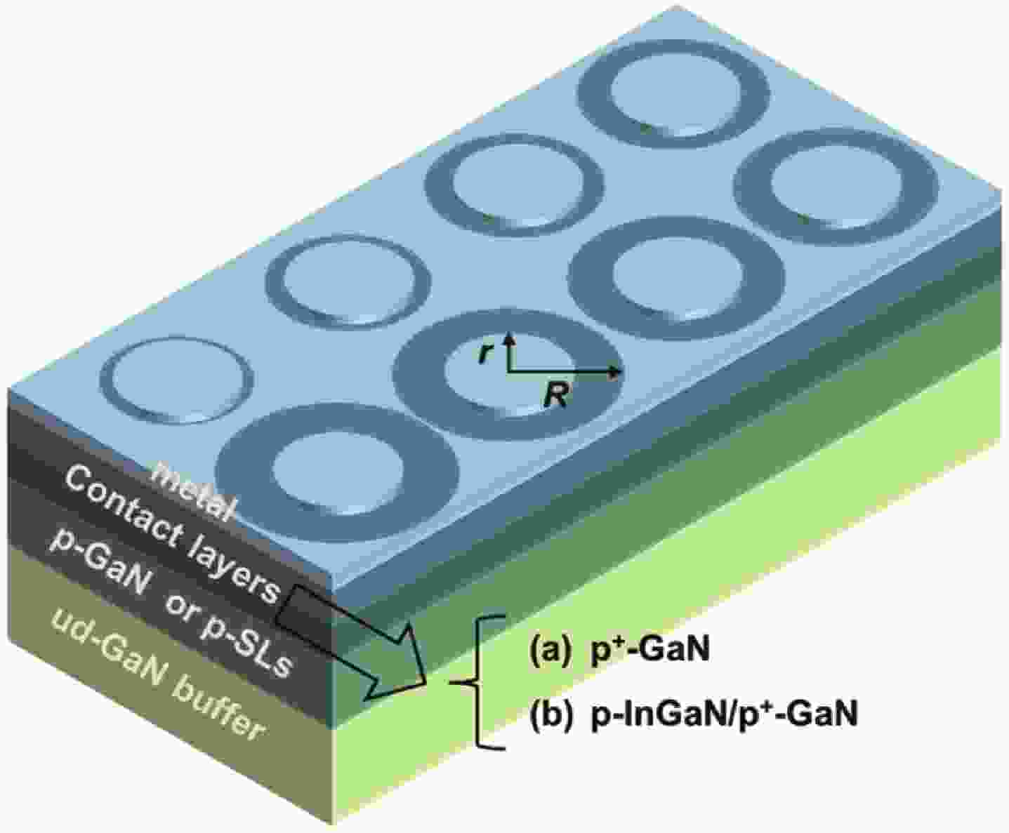
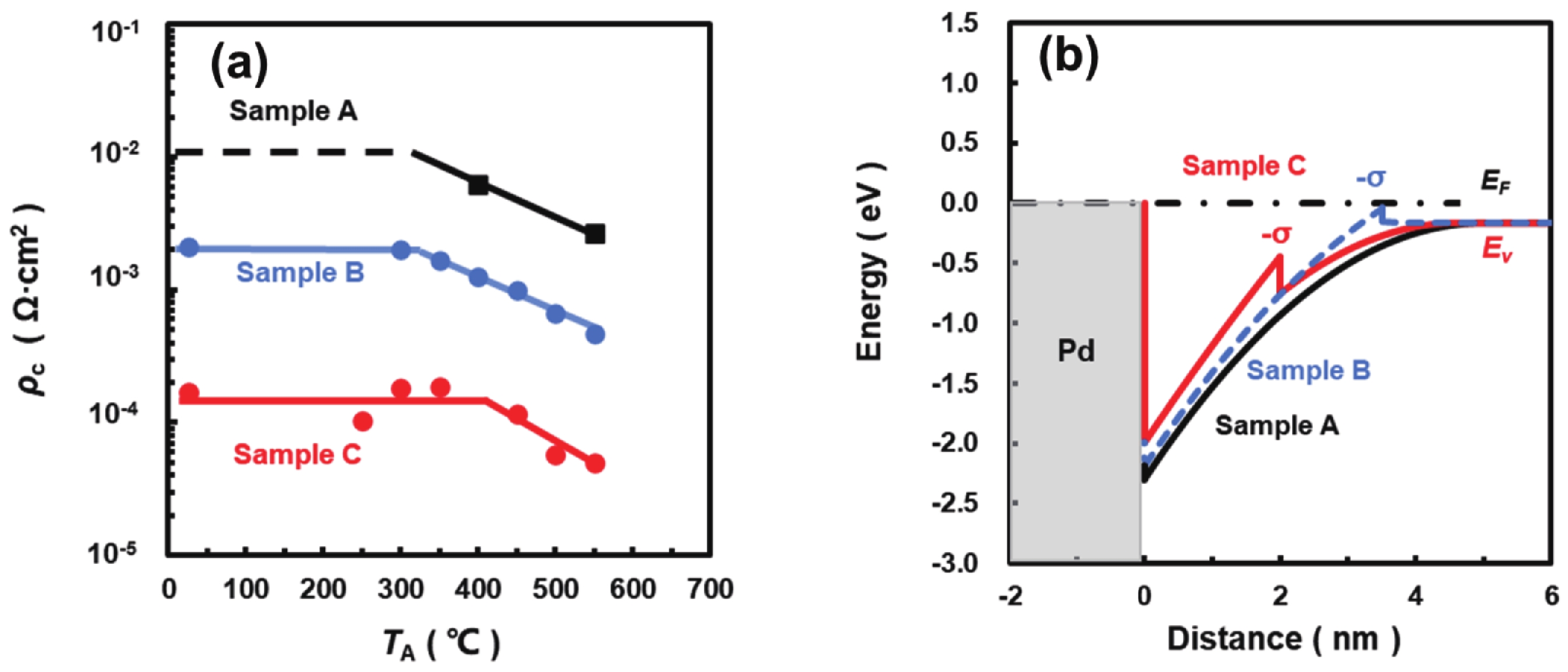
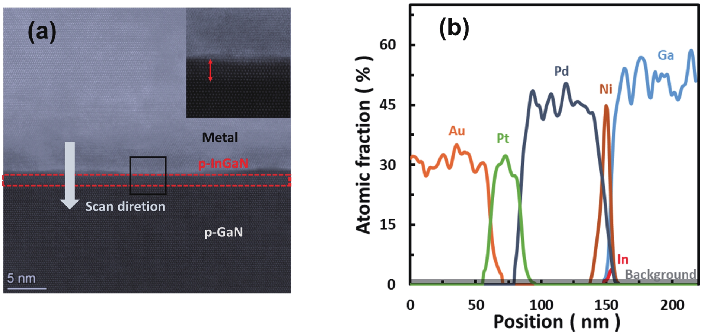
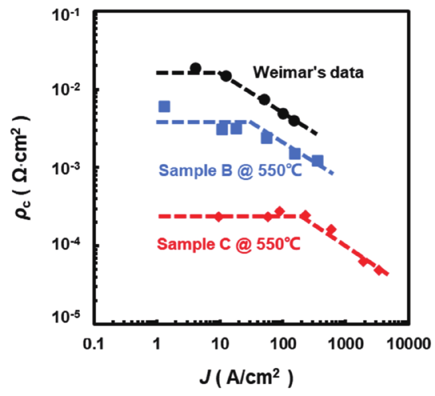
Specific contact resistance

J. Semicond.
2022, 43(9): 092201 doi: 10.1088/1674-4926/43/9/092201
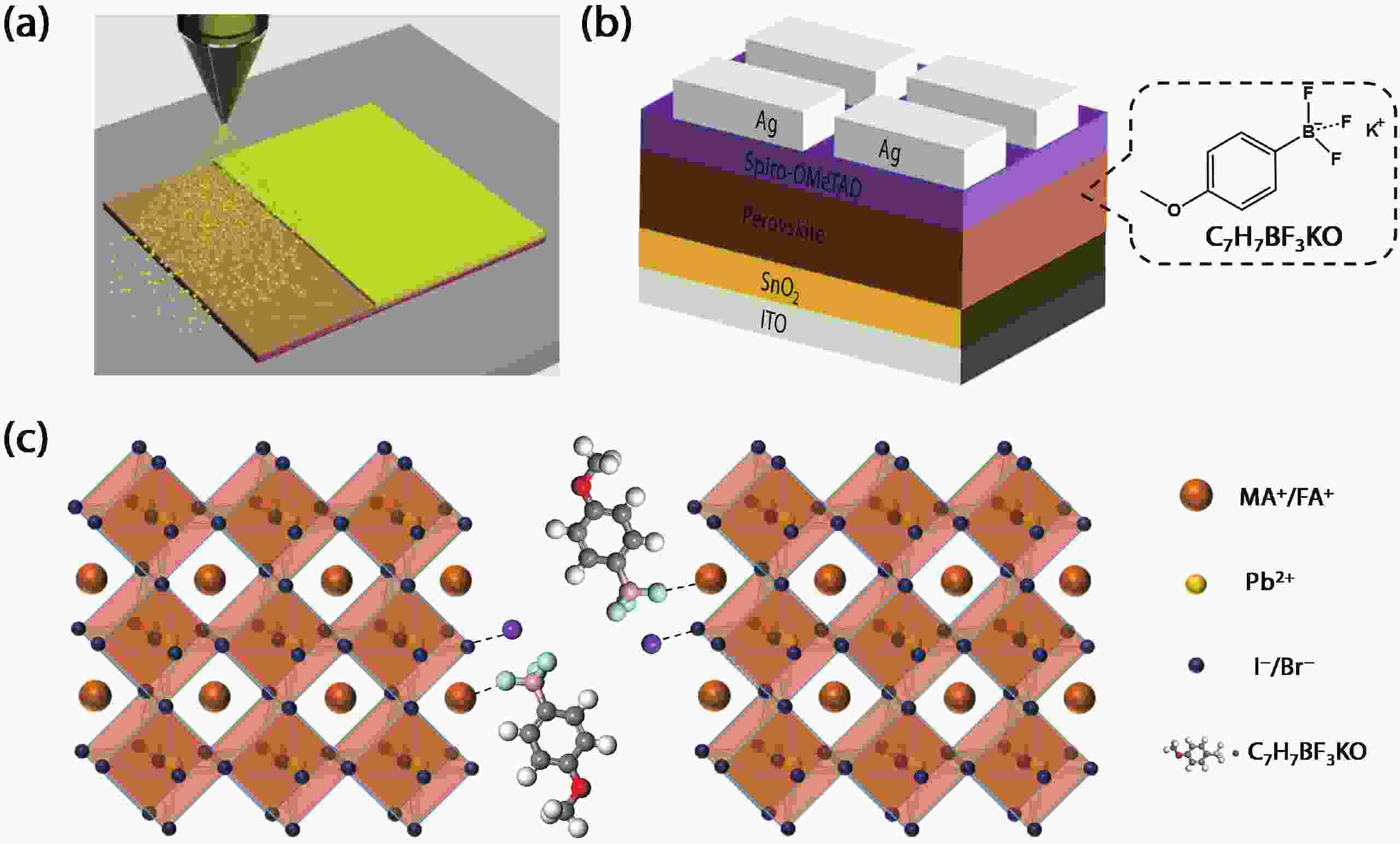
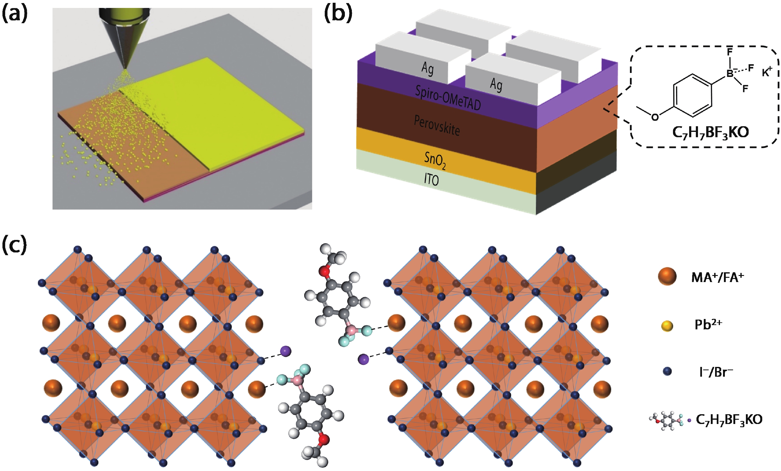
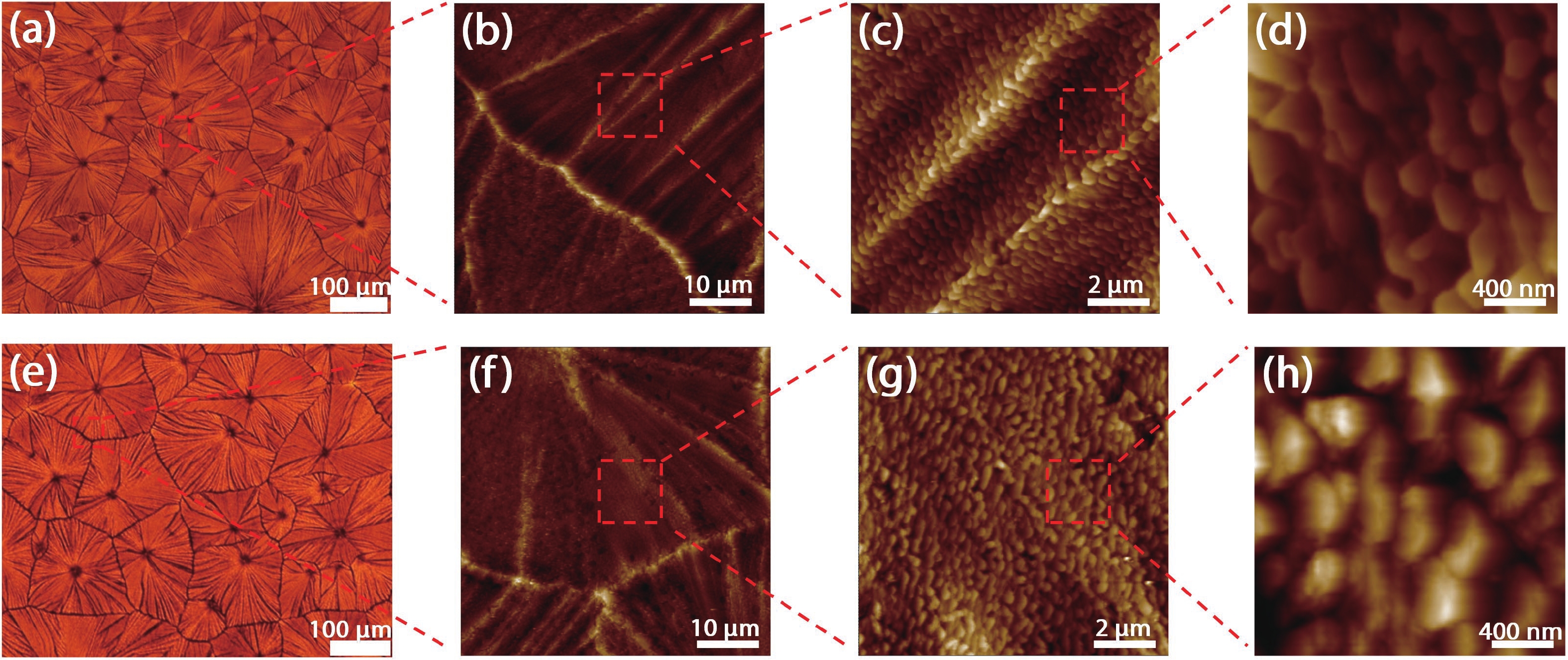
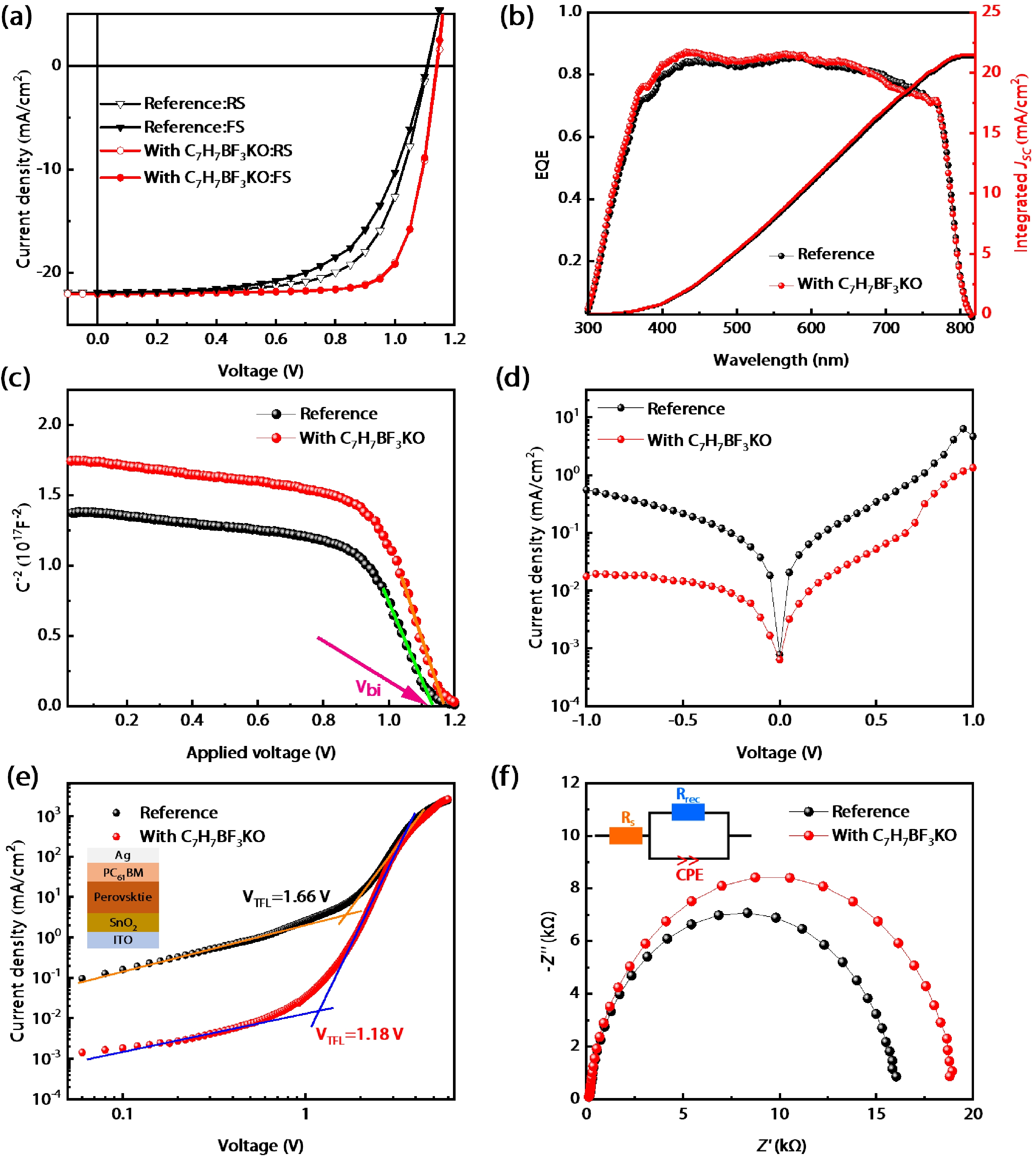
Defects as non-radiative recombination centers hinder the further efficiency improvements of perovskite solar cells (PSCs). Additive engineering has been demonstrated to be an effective method for defect passivation in perovskite films. Here, we employed (4-methoxyphenyl) potassium trifluoroborate (C7H7BF3KO) with ${{\rm{BF}}_3^-}$ and K+ functional groups to passivate spray-coated (FAPbI3)x(MAPbBr3)1–x perovskite and eliminate hysteresis. It is shown that the F of ${{\rm{BF}}_3^-}$ can form hydrogen bonds with the H atom in the amino group of MA+/FA+ ions of perovskite, thus reducing the generation of MA+/FA+ vacancies and improving device efficiency. Meanwhile, K+ and reduced MA+/FA+ vacancies can inhibit ion migration, thereby eliminating hysteresis. With the aid of C7H7BF3KO, we obtained hysteresis-free PSCs with the maximum efficiency of 19.5% by spray-coating in air. Our work demonstrates that additive engineering is promising to improve the performance of spray-coated PSCs.