Issue Browser
Volume 43, Issue 11,
Nov 2022
Column


J. Semicond.
2022, 43(11): 113101 doi: 10.1088/1674-4926/43/11/113101
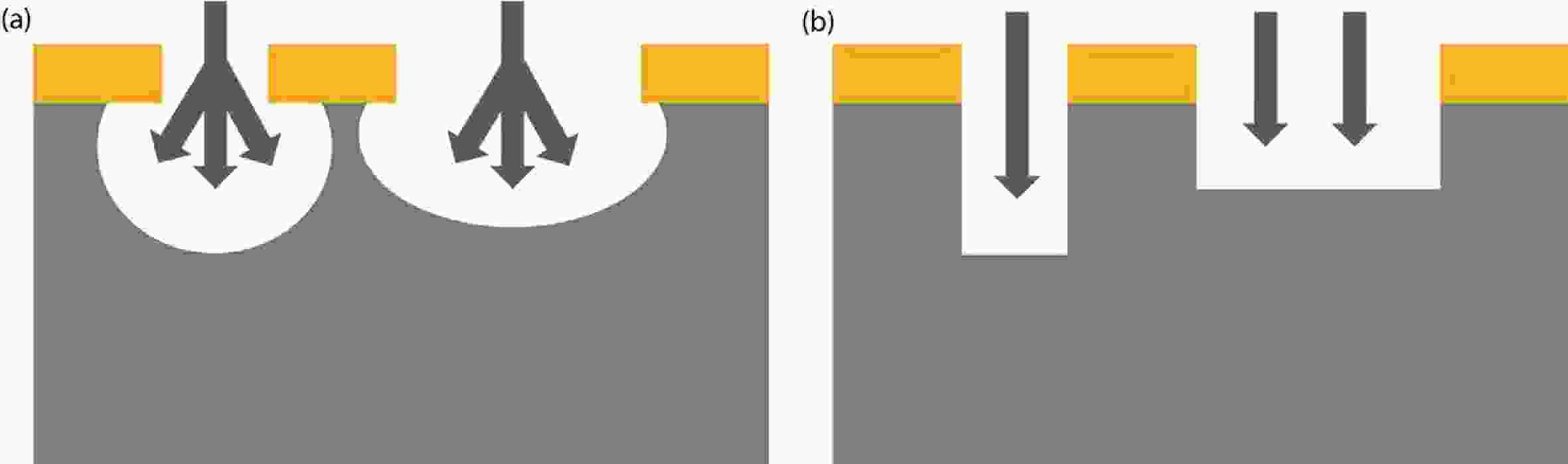
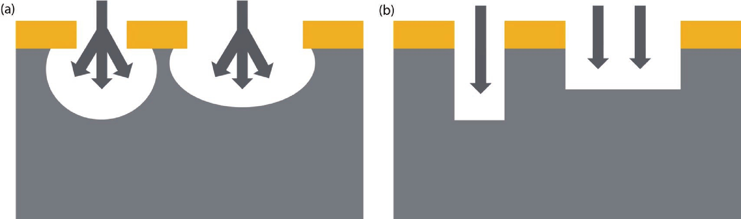
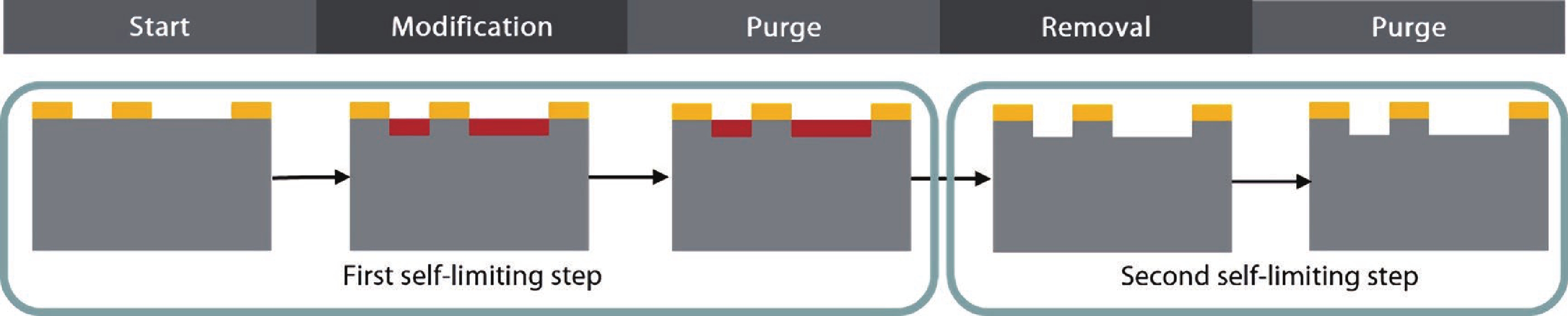
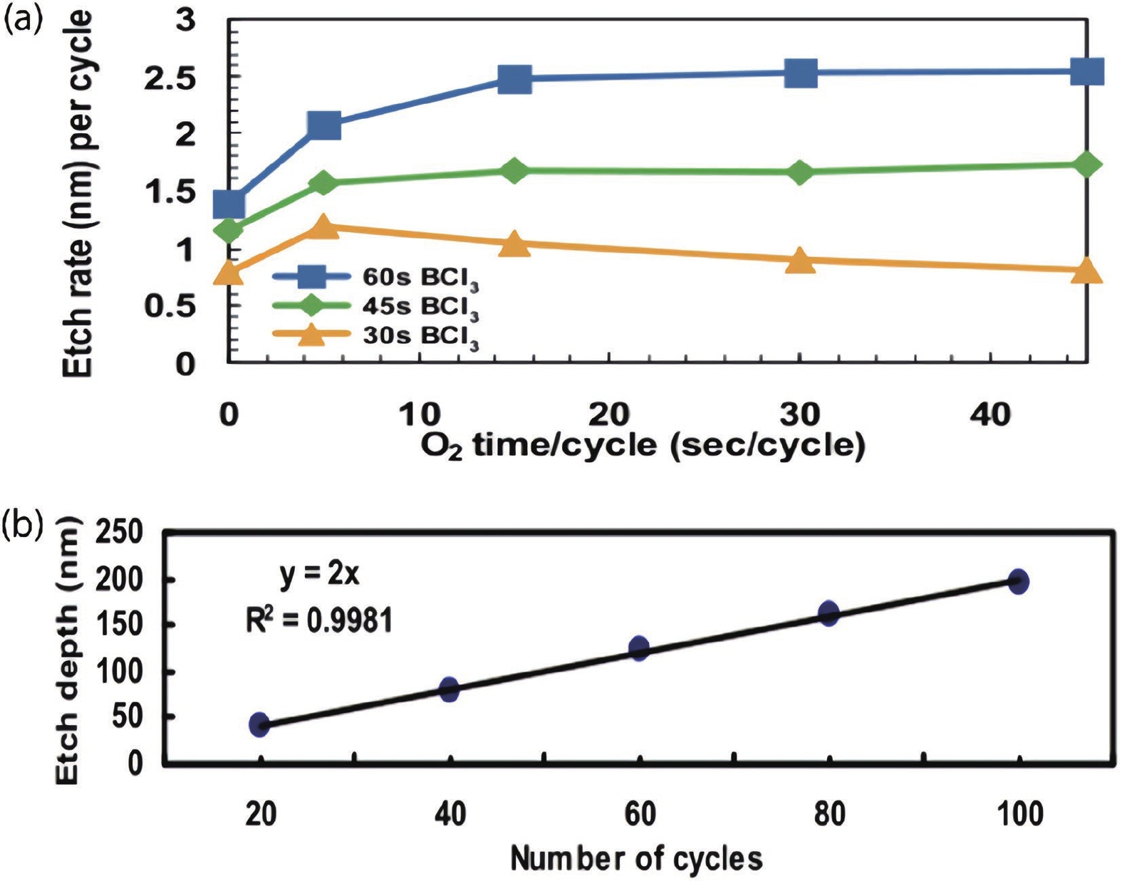
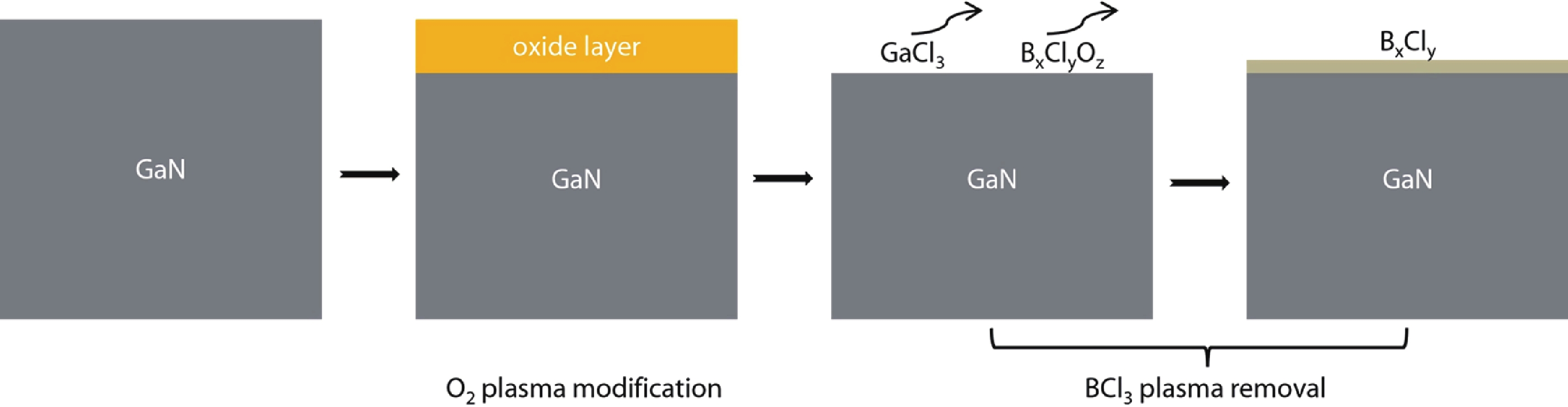
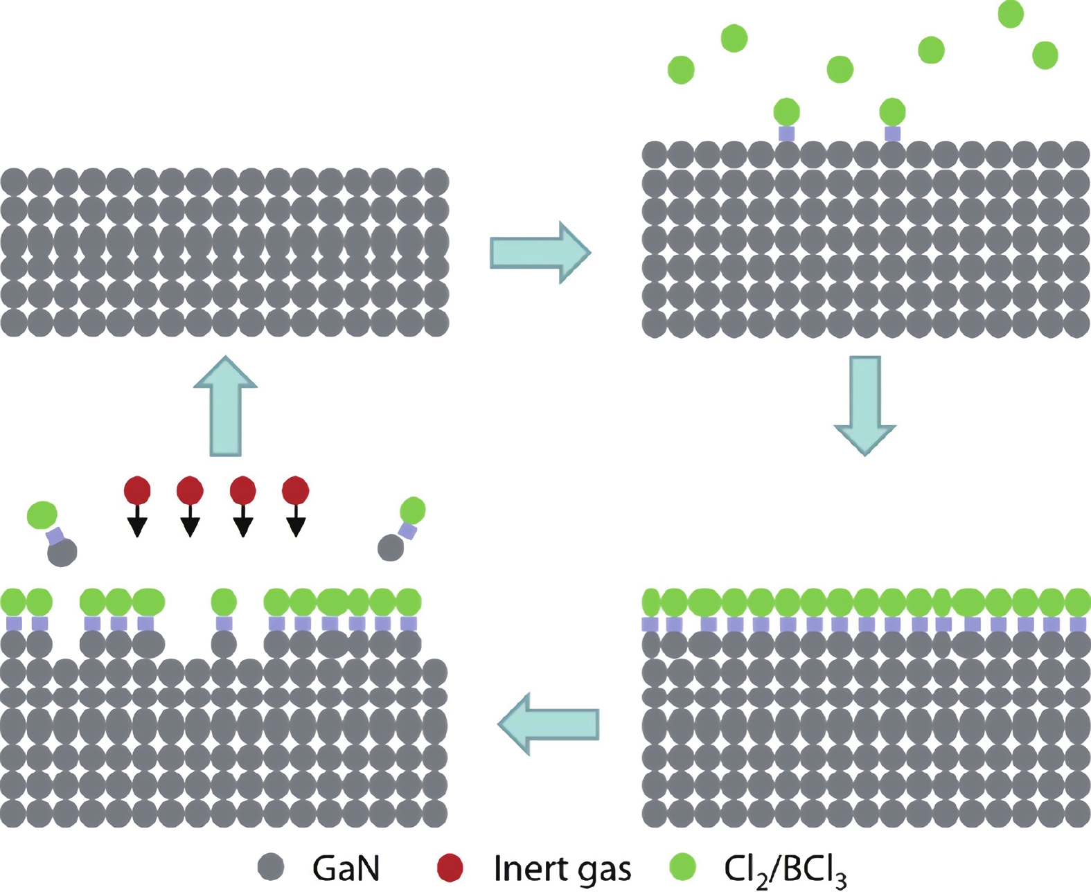
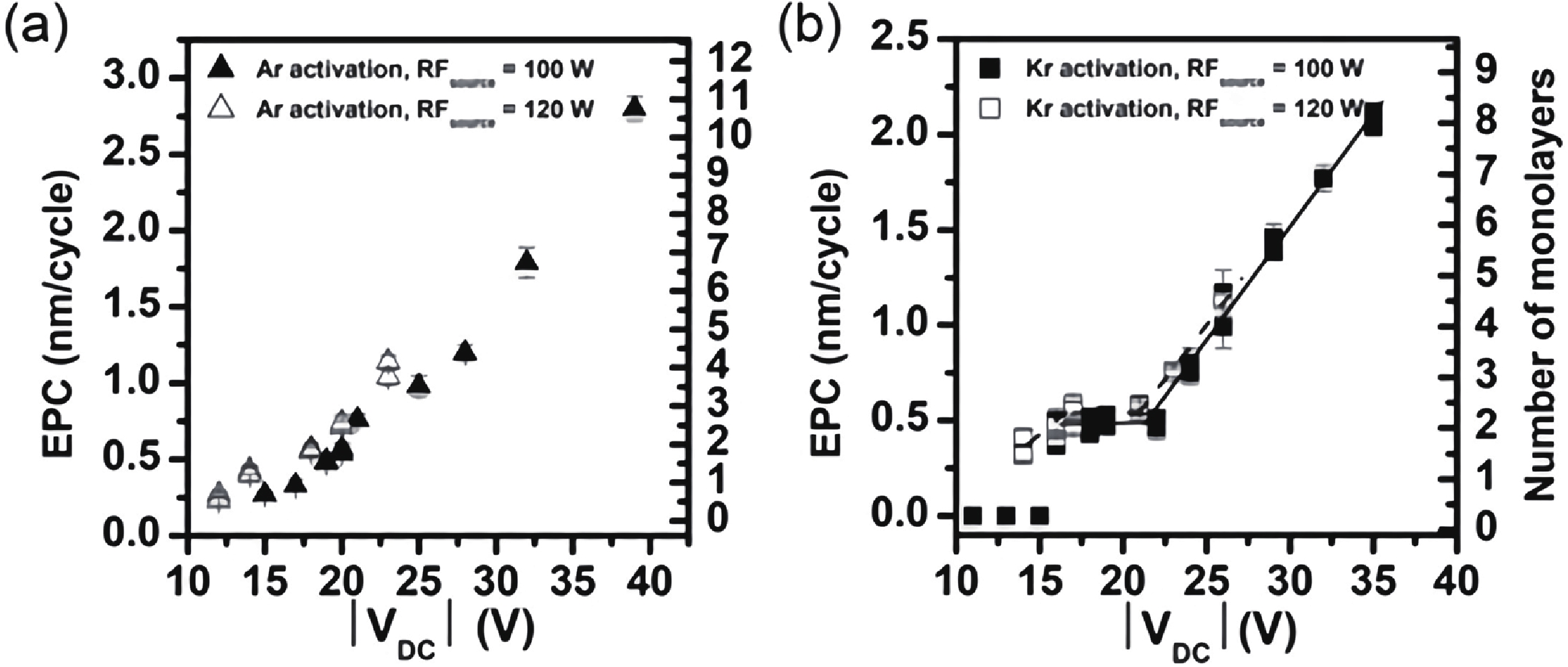
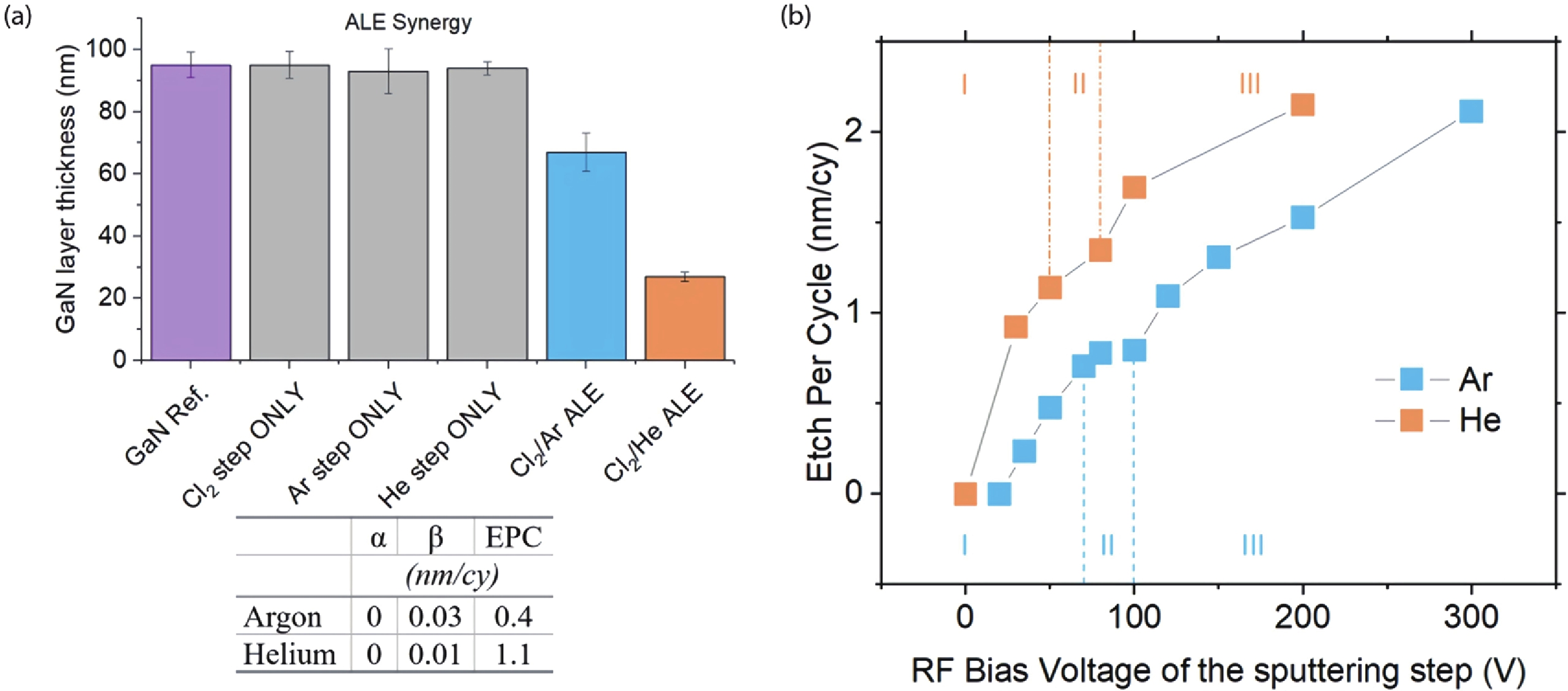
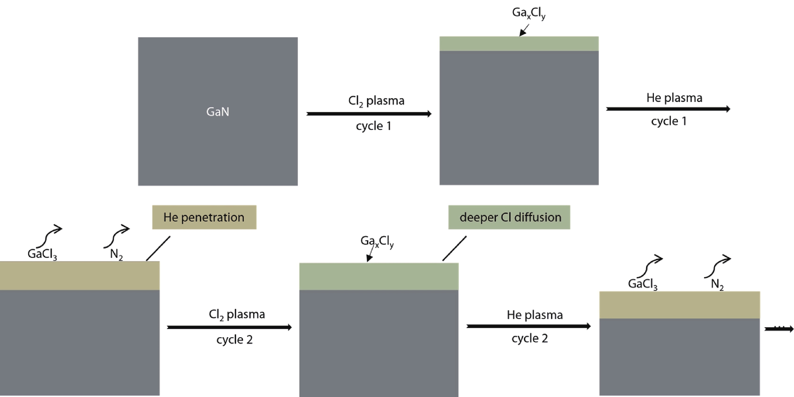
With the development of the third generation of semiconductor devices, it is essential to achieve precise etching of gallium nitride (GaN) materials that is close to the atomic level. Compared with the traditional wet etching and continuous plasma etching, plasma atomic layer etching (ALE) of GaN has the advantages of self-limiting etching, high selectivity to other materials, and smooth etched surface. In this paper the basic properties and applications of GaN are presented. It also presents the various etching methods of GaN. GaN plasma ALE systems are reviewed, and their similarities and differences are compared. In addition, the industrial application of GaN plasma ALE is outlined.


J. Semicond.
2022, 43(11): 112301 doi: 10.1088/1674-4926/43/11/112301

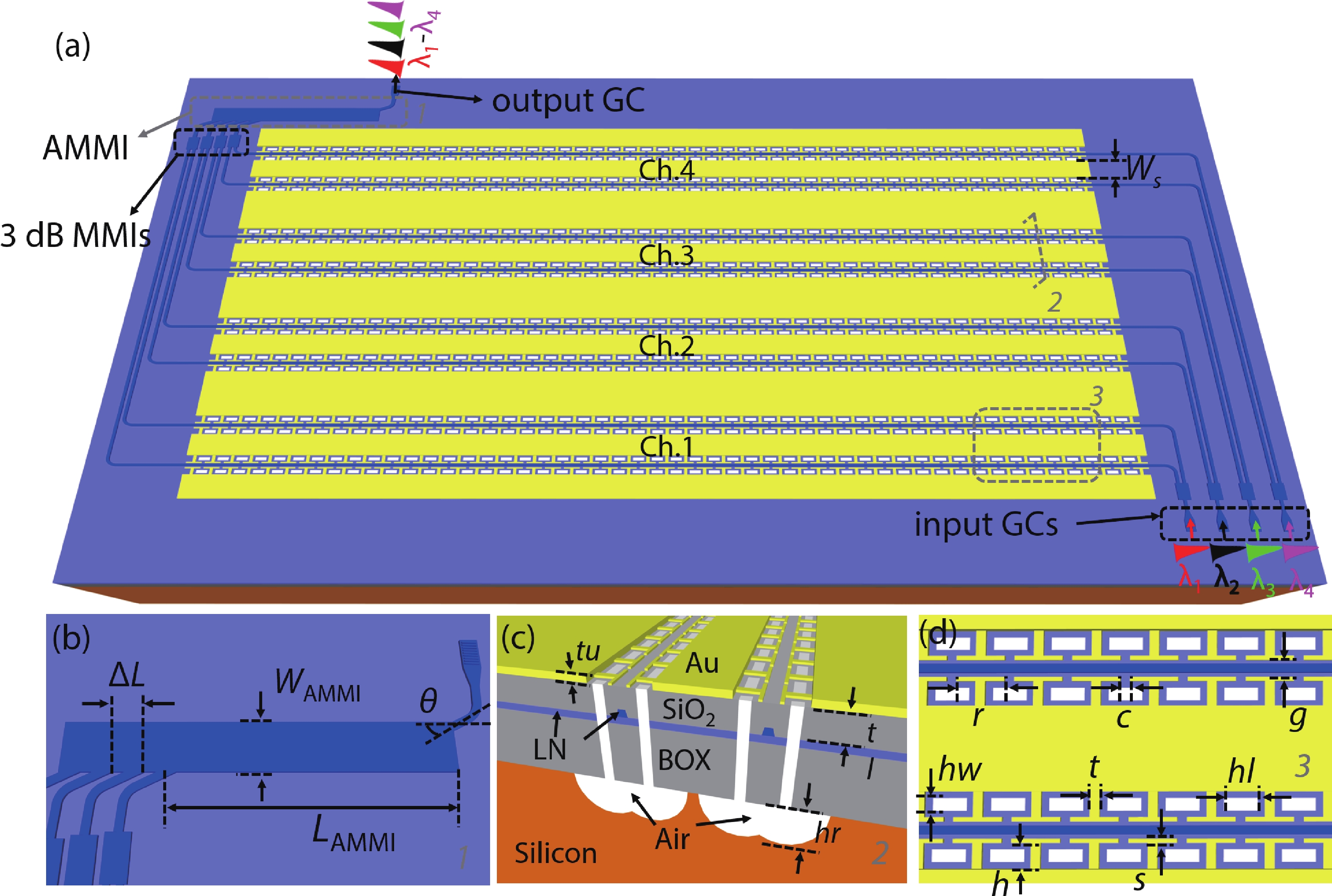
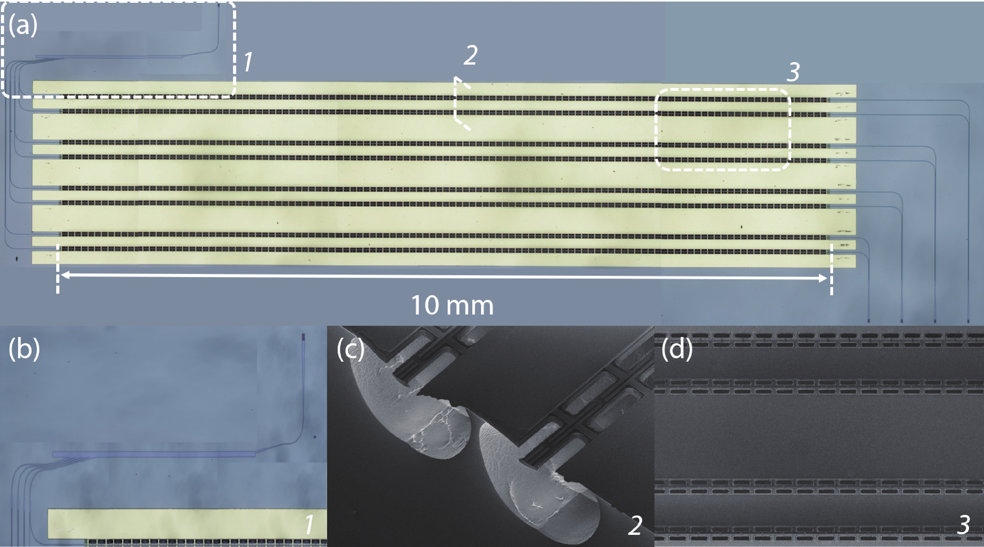
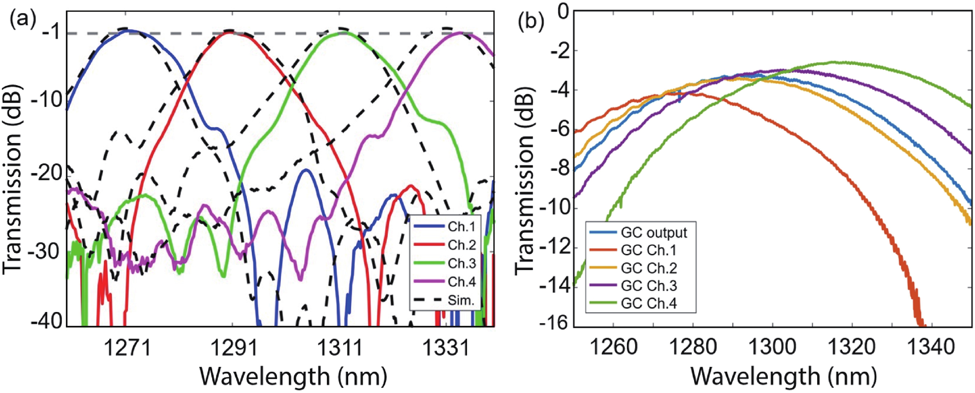
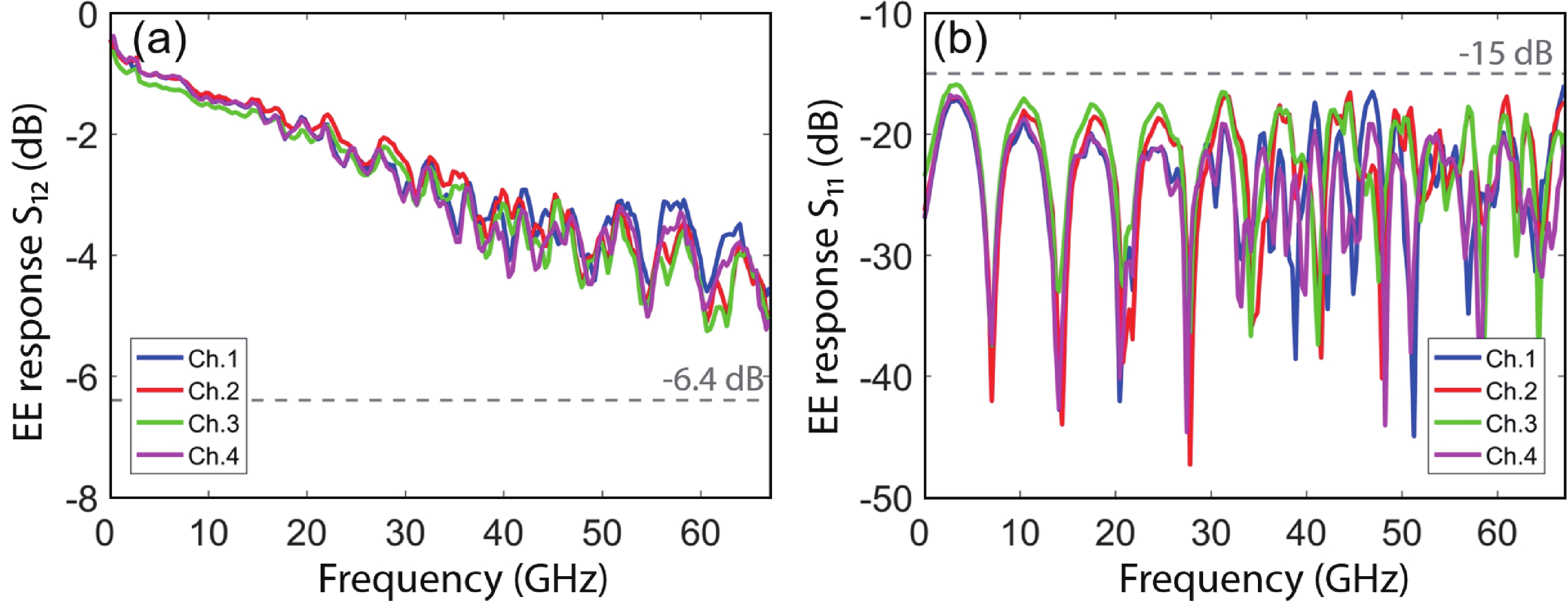
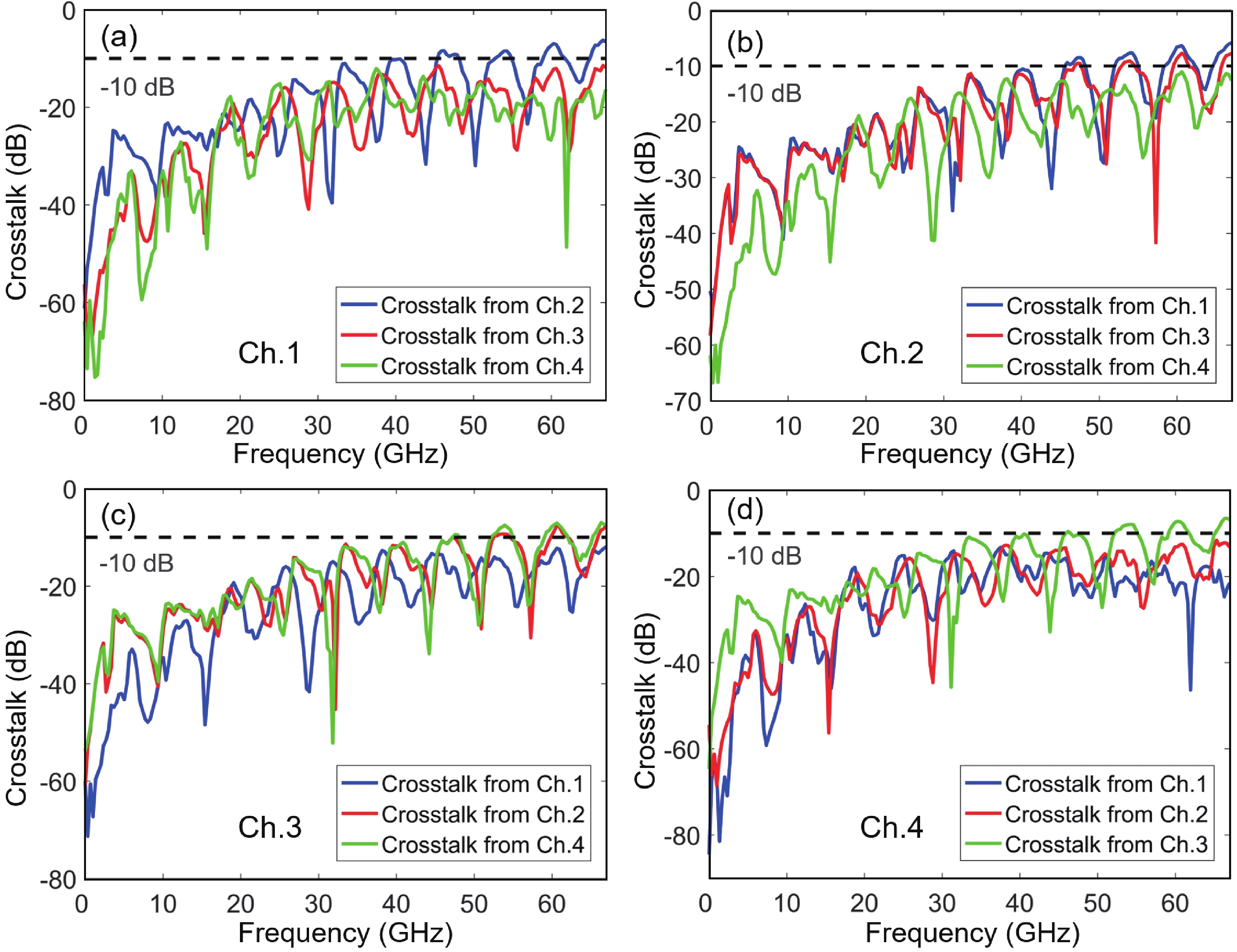
Multi-lane integrated transmitter chips are key components in future compact optical modules to realize high-speed optical interconnects. Thin-film lithium niobate (TFLN) photonics have emerged as a promising platform for achieving high-performance chip-scale optical systems. Combining a coarse wavelength-division multiplexing (CWDM) devices using fabrication-tolerant angled multimode interferometer structure and high-performance electro-optical modulators, we demonstrate monolithic on-chip four-channel CWDM transmitter on the TFLN platform for the first time. The four-channel CWDM transmitter enables high-speed transmissions of 100 Gb/s data rate per wavelength channel (i.e., an aggregated date rate of 400 Gb/s).


J. Semicond.
2022, 43(11): 112501 doi: 10.1088/1674-4926/43/11/112501
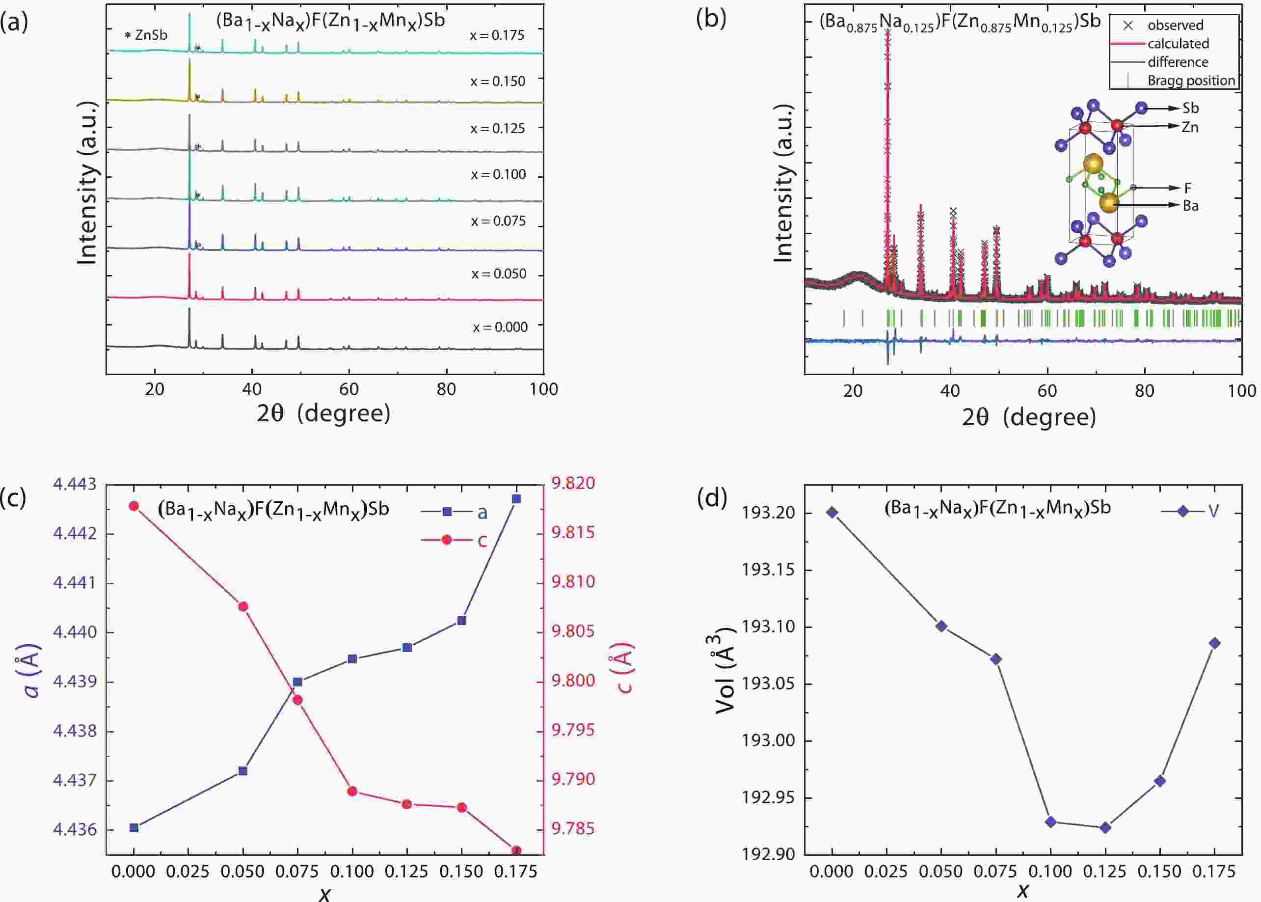
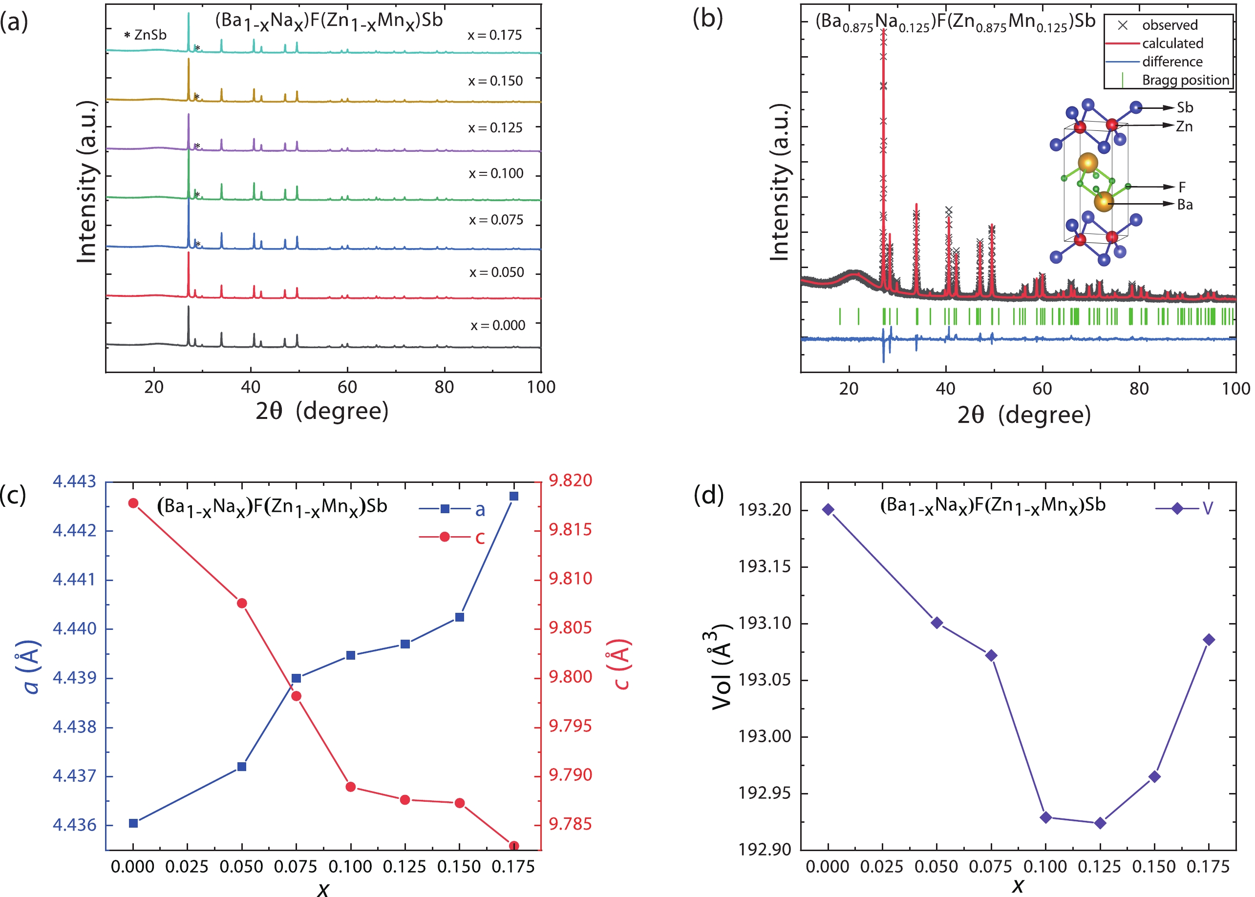
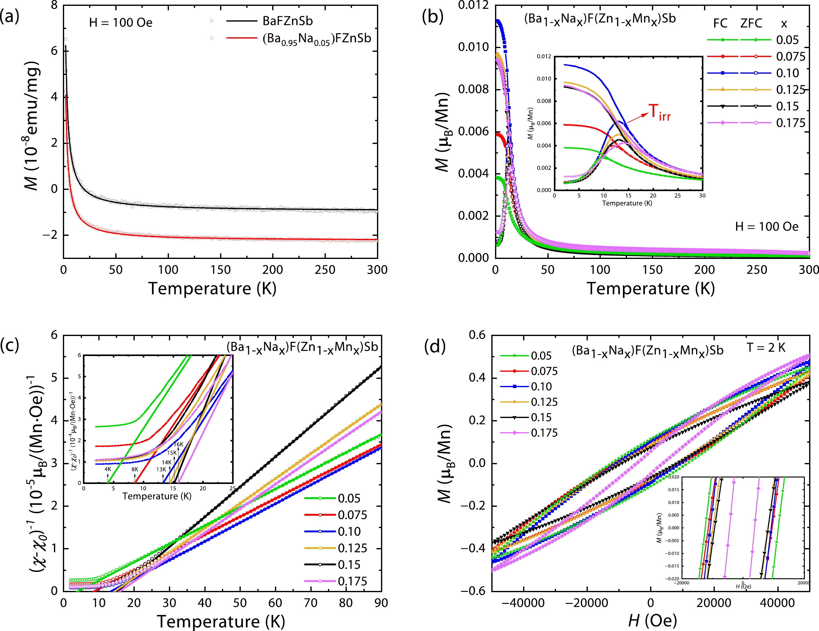
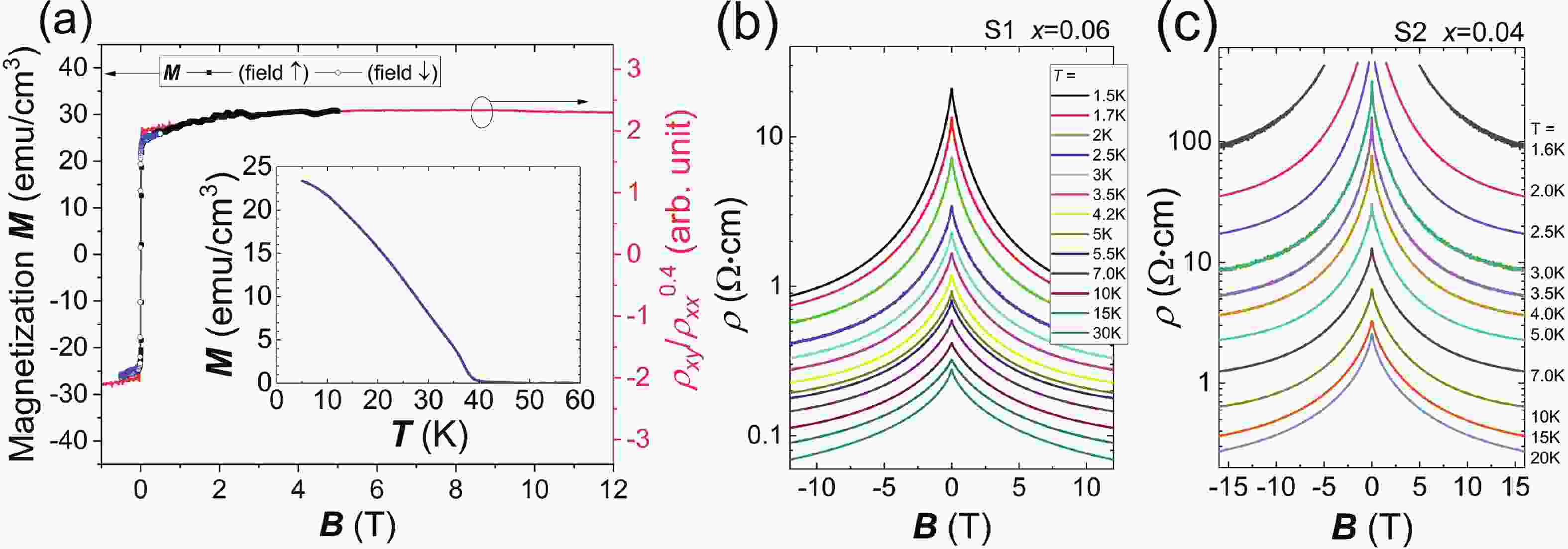
We report the successful synthesis and characterization of a novel 1111-type magnetic semiconductor (Ba1−xNax)F(Zn1−xMnx)Sb (0.05 ≤ x ≤ 0.175) with tetragonal ZrSiCuAs-type structure, which is isostructural to the layered iron-based superconductor La(O,F)FeAs. Na substitutions for Ba and Mn substitutions for Zn introduce carriers and local magnetic moments, respectively. Ferromagnetic interaction is formed when Na and Mn are codoped, demonstrating that local magnetic moments are mediated by carriers. Iso-thermal magnetization shows that the coercive field is as large as ~ 12 000 Oe, which is also reflected in the large split between the temperature-dependent magnetization in zero-field-cooling and field-cooling condition. AC susceptibility under zero field demonstrates that samples evolve into spin-glass state below spin freezing temperature Tf. The measurements of temperature-dependent resistivity indicate that (Ba1−xNax)F(Zn1−xMnx)Sb exhibits semiconducting behaviour.


J. Semicond.
2022, 43(11): 112701 doi: 10.1088/1674-4926/43/11/112701
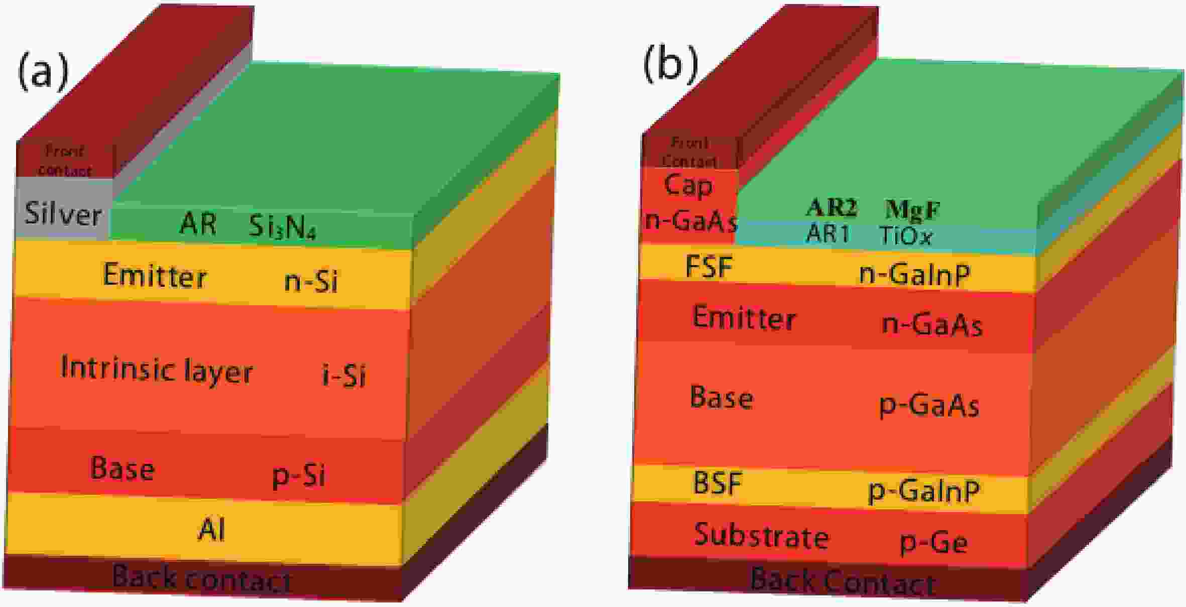
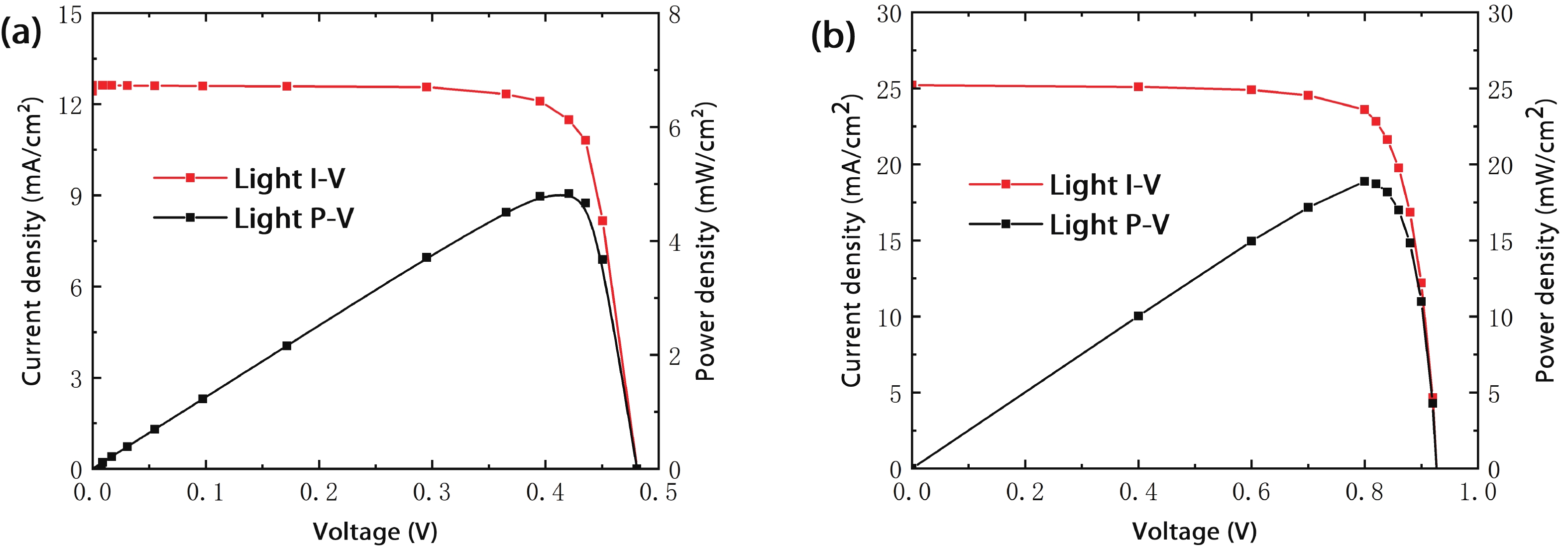
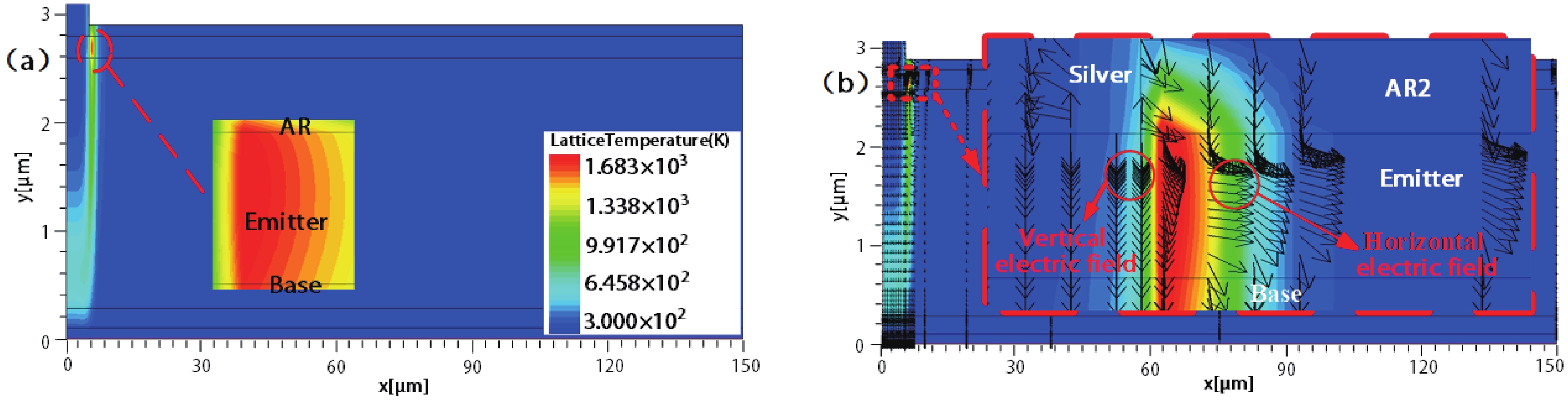
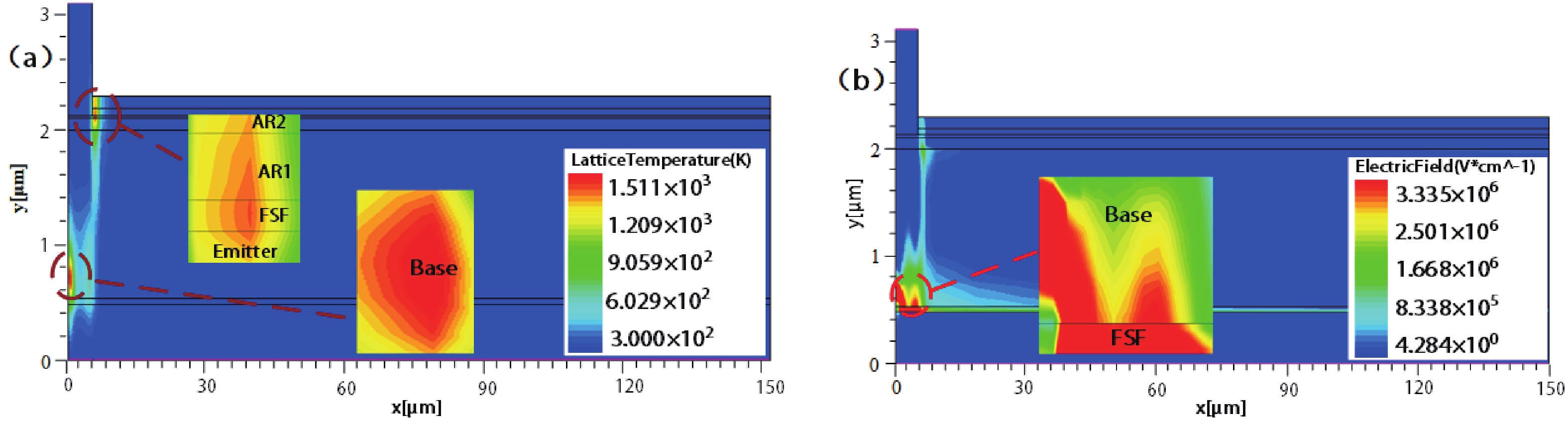
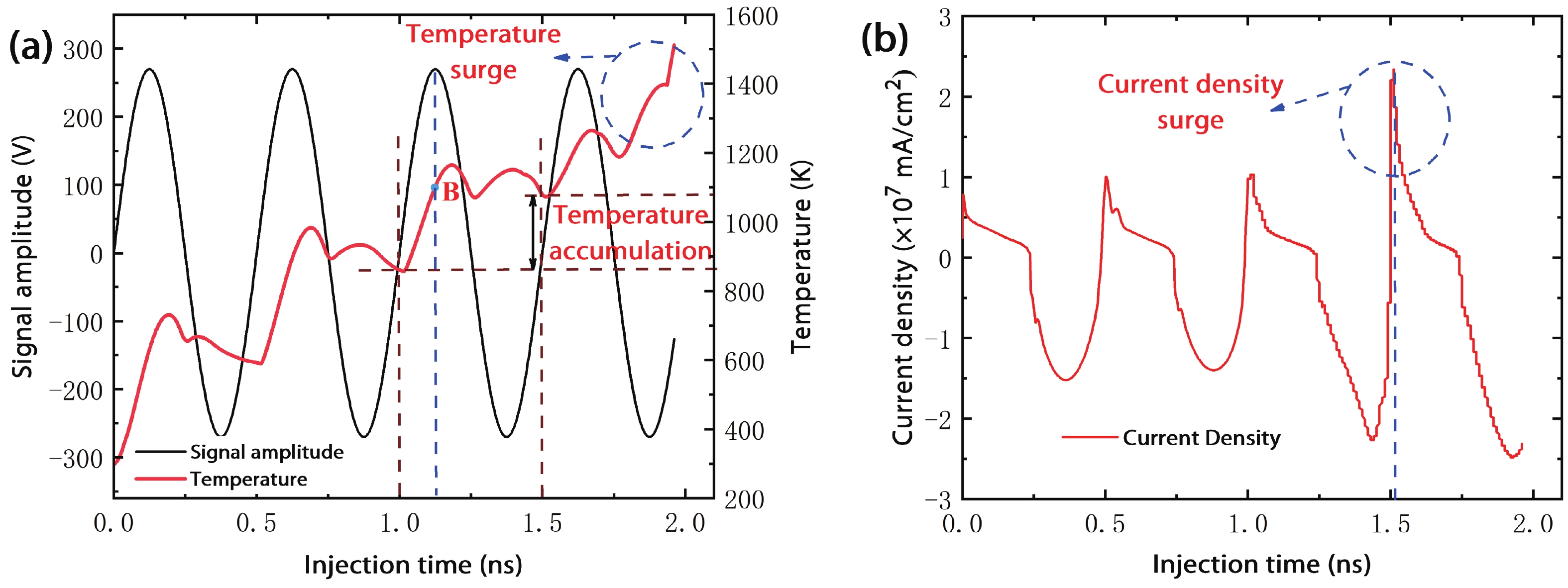
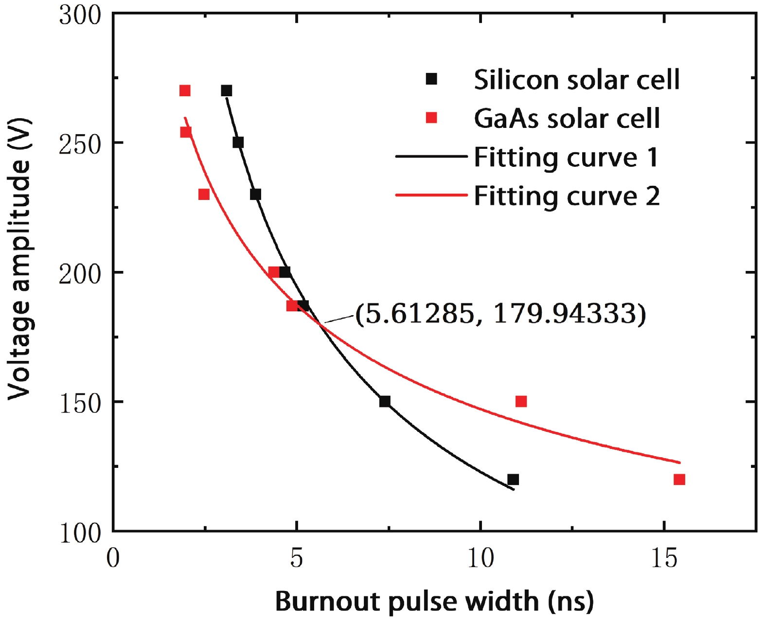
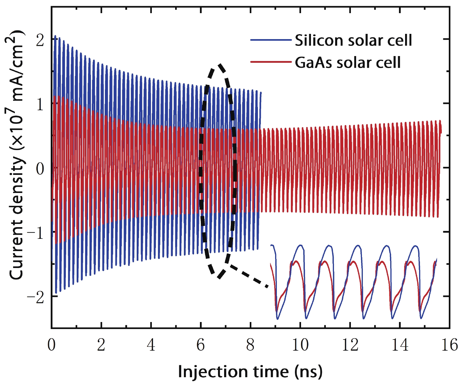
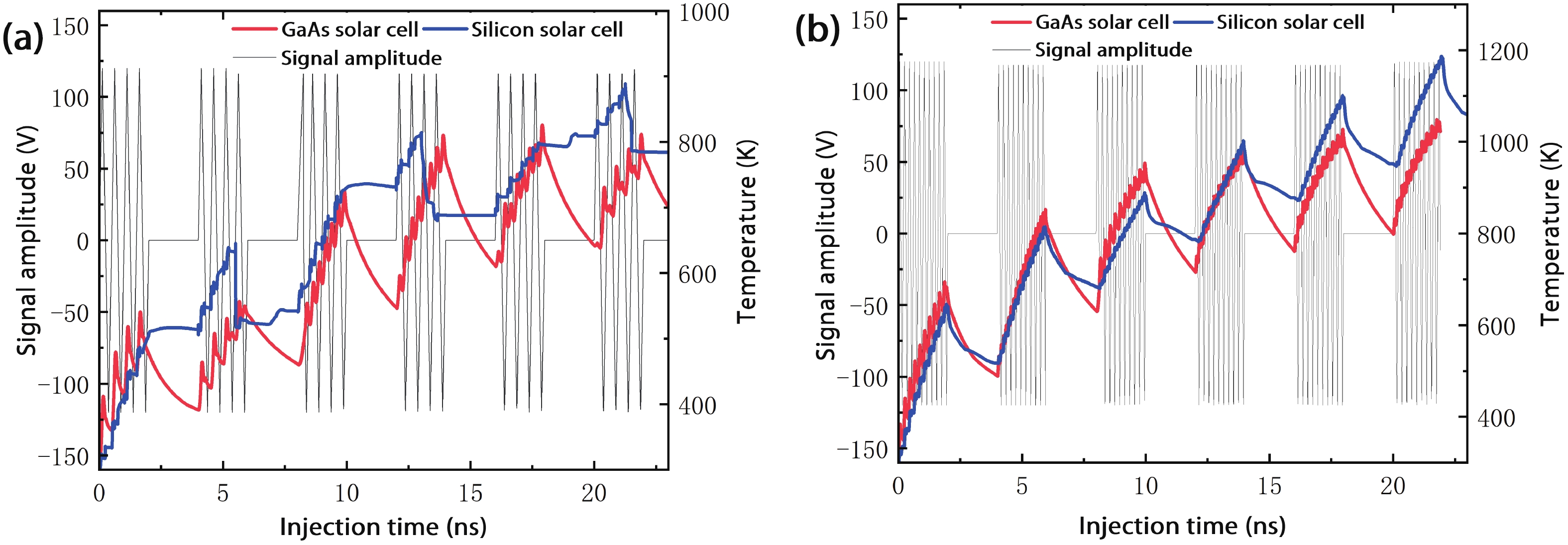
The high-power microwave (HPM) effect heats solar cells, which is an important component of a satellite. This creates a serious reliability problem and affects the normal operation of a satellite. In this paper, the different HPM response characteristics of two kinds of solar cells are comparatively researched by simulation. The results show that there are similarities and differences in hot spot distribution and damage mechanisms between both kinds of solar cell, which are related to the amplitude of HPM. In addition, the duty cycle of repetition frequency contributes more to the temperature accumulation of the solar cells than the carrier frequency. These results will help future research of damage assessment technology, reliability enhancement and the selection of materials for solar cells.


J. Semicond.
2022, 43(11): 112801 doi: 10.1088/1674-4926/43/11/112801
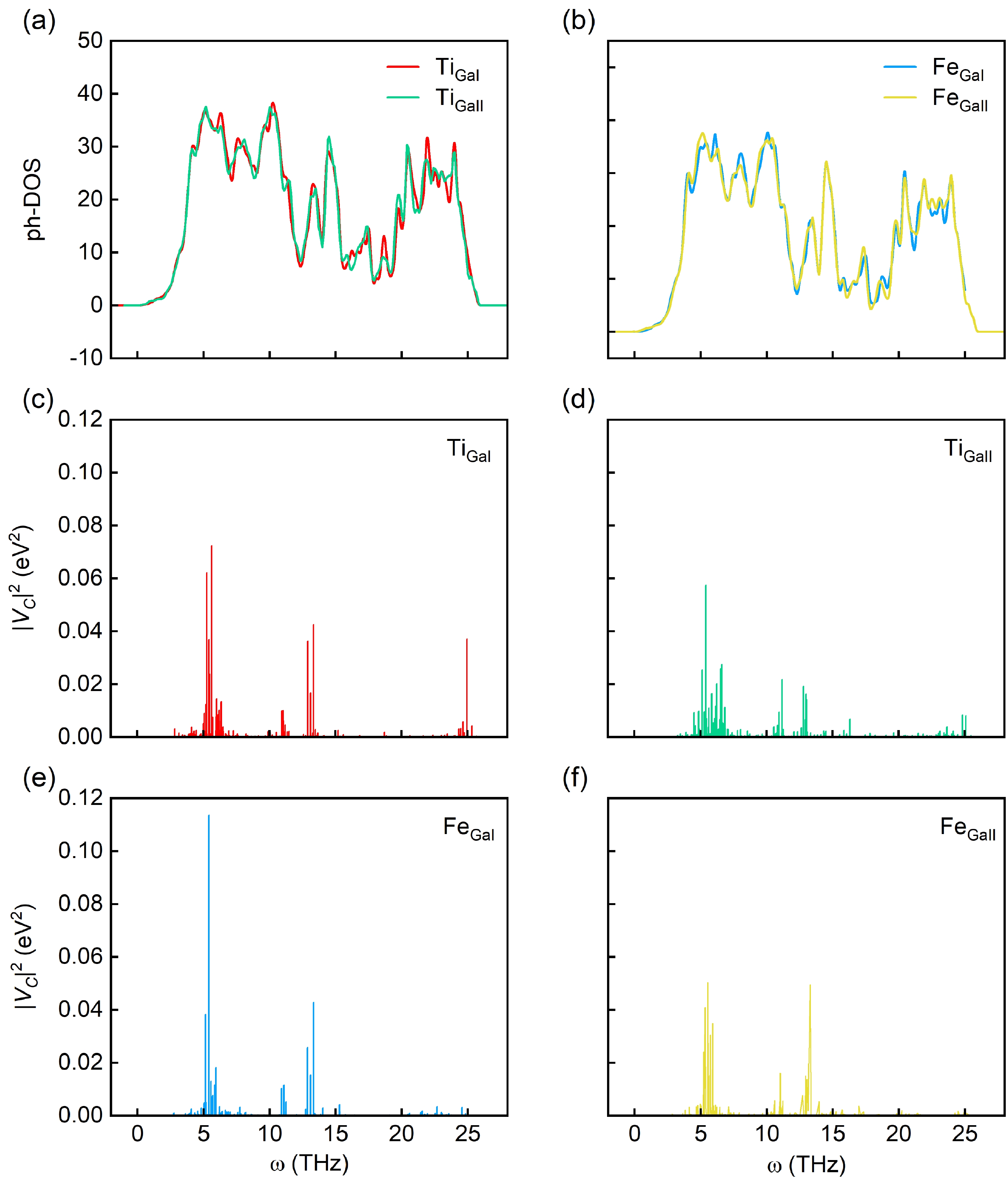
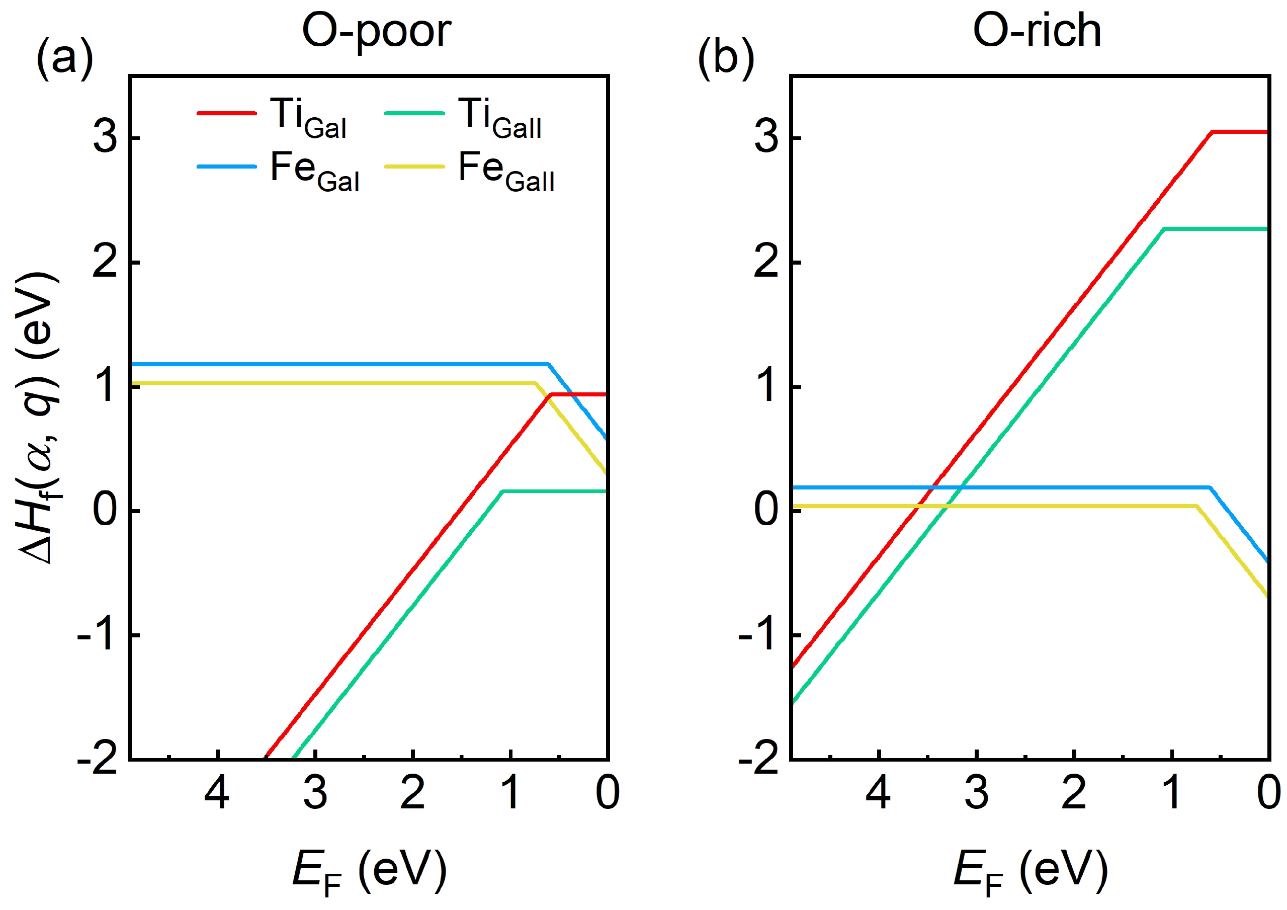
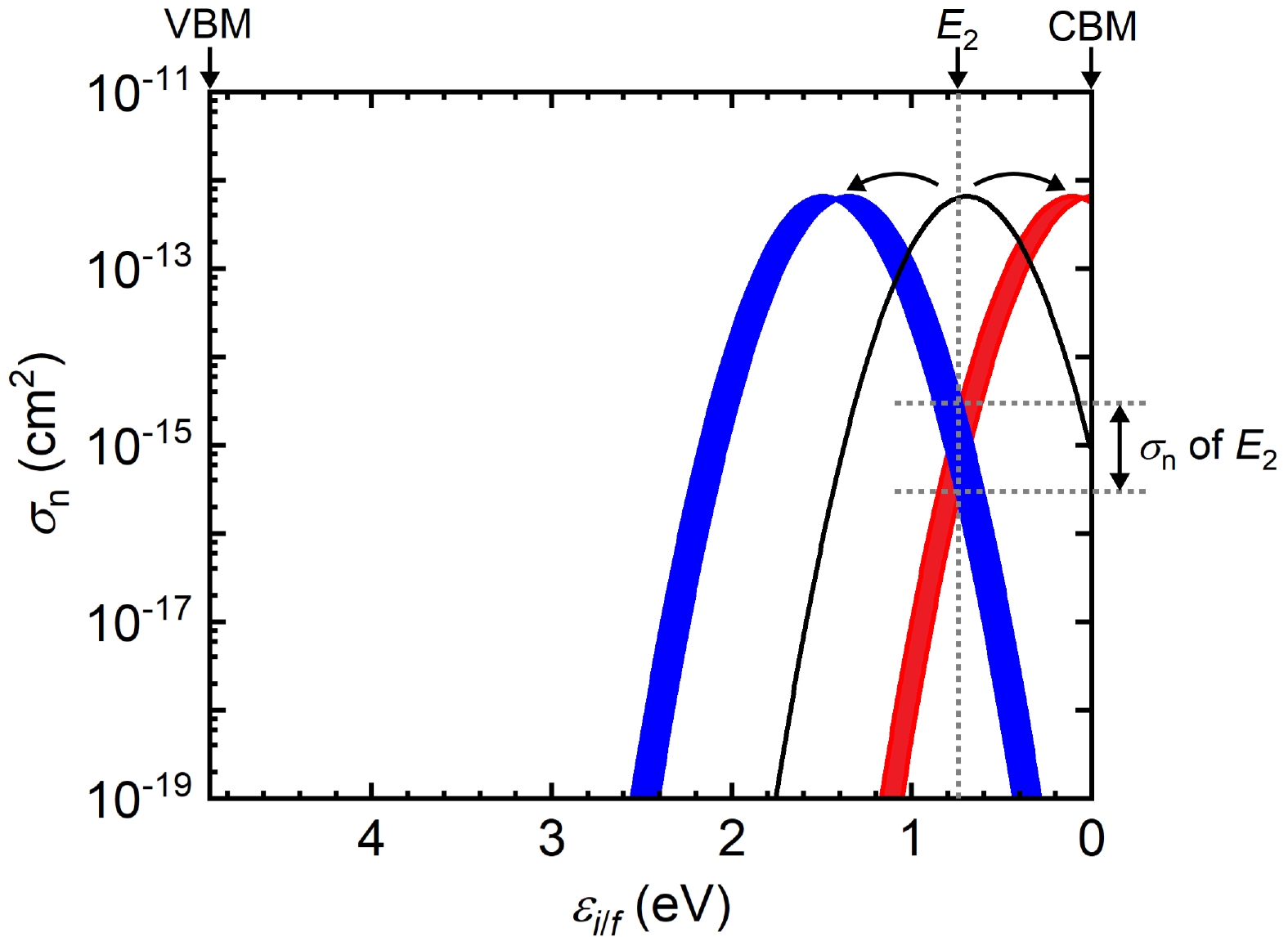
The emerging wide bandgap semiconductor


J. Semicond.
2022, 43(11): 114101 doi: 10.1088/1674-4926/43/11/114101
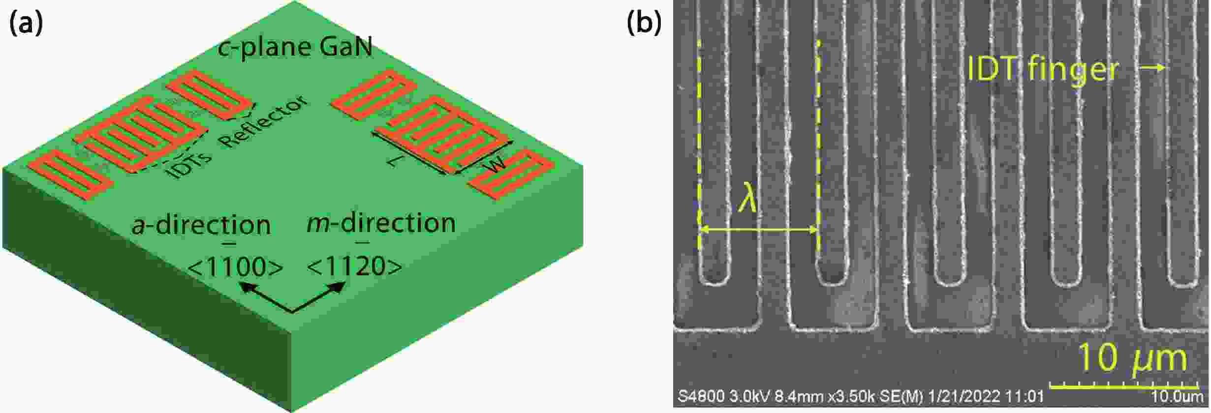
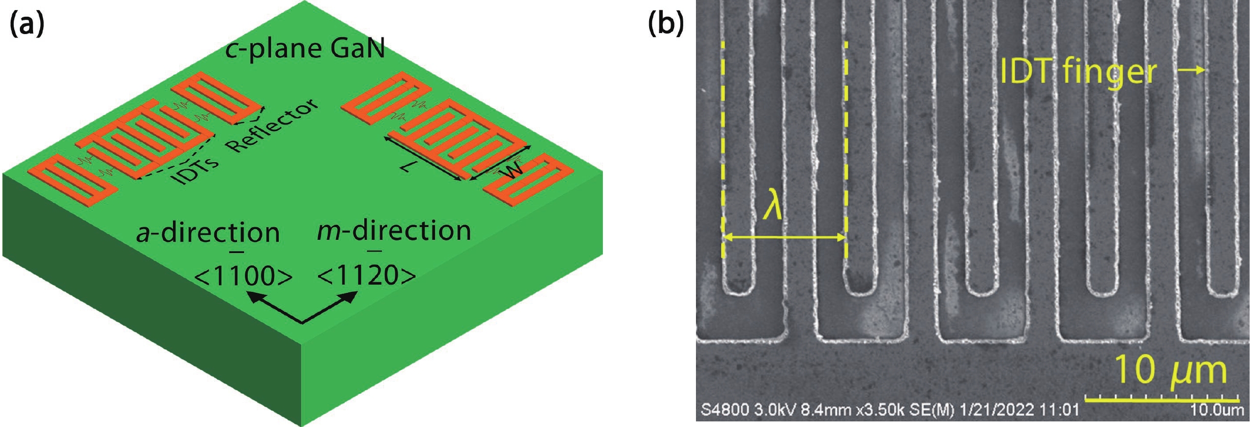
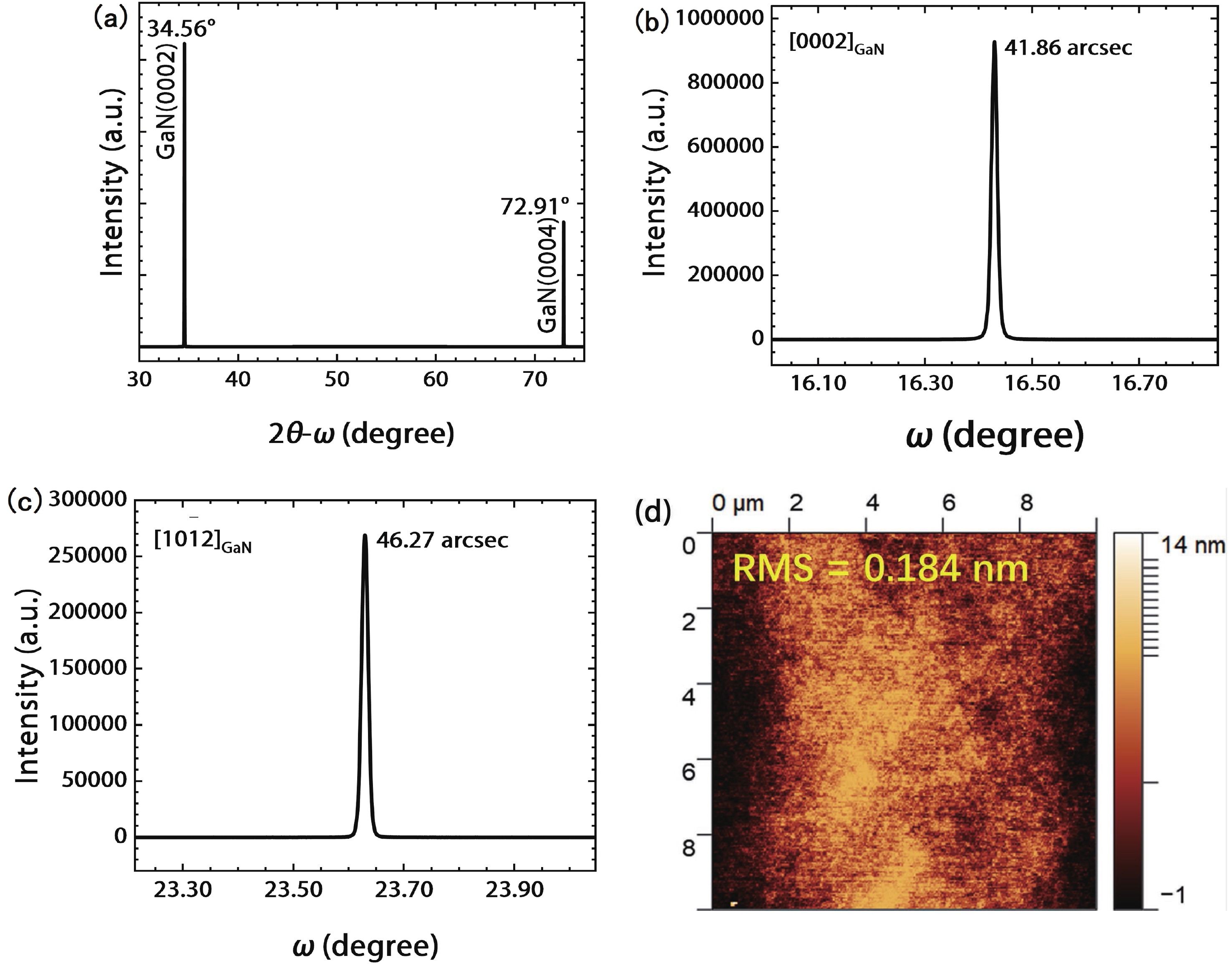
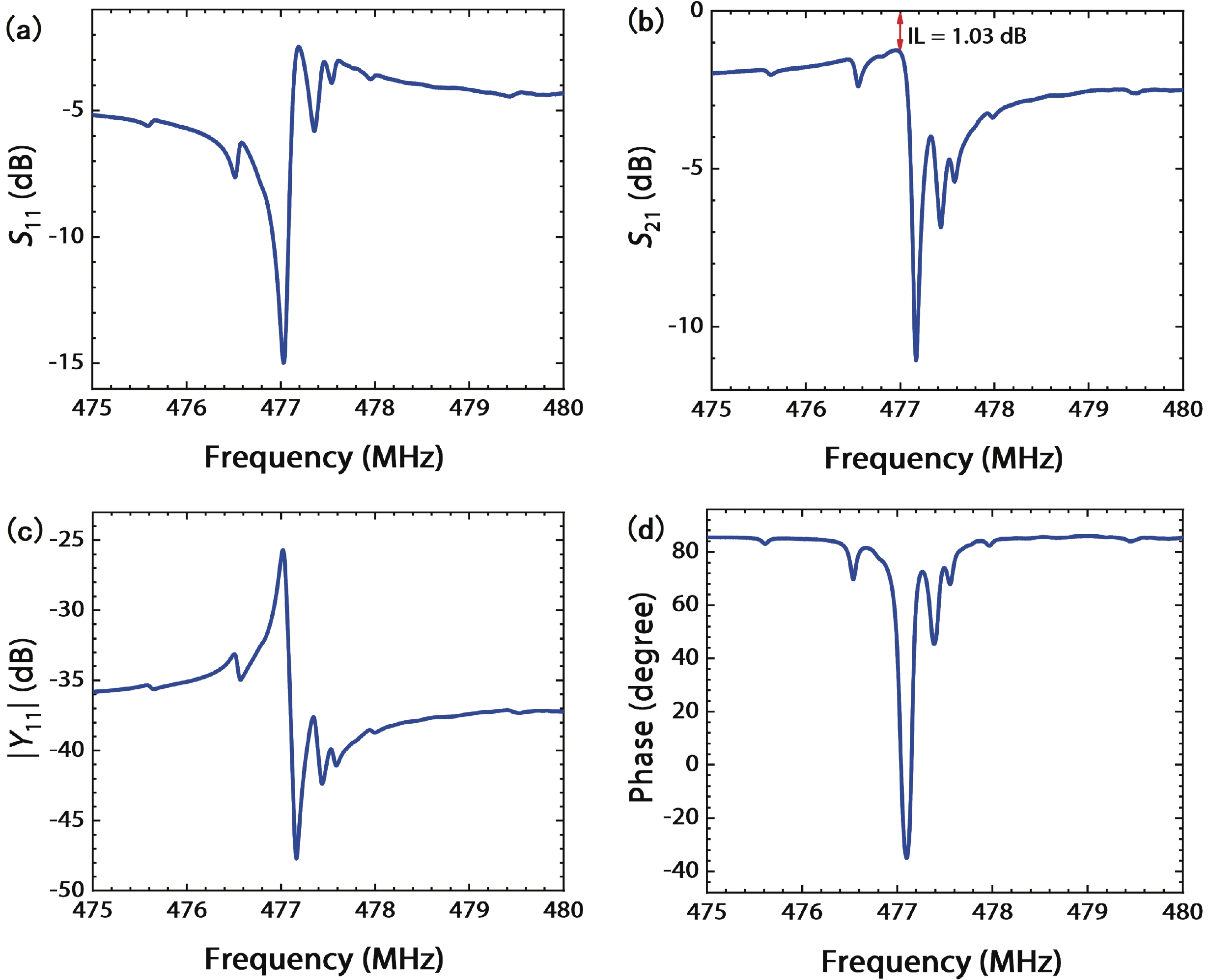
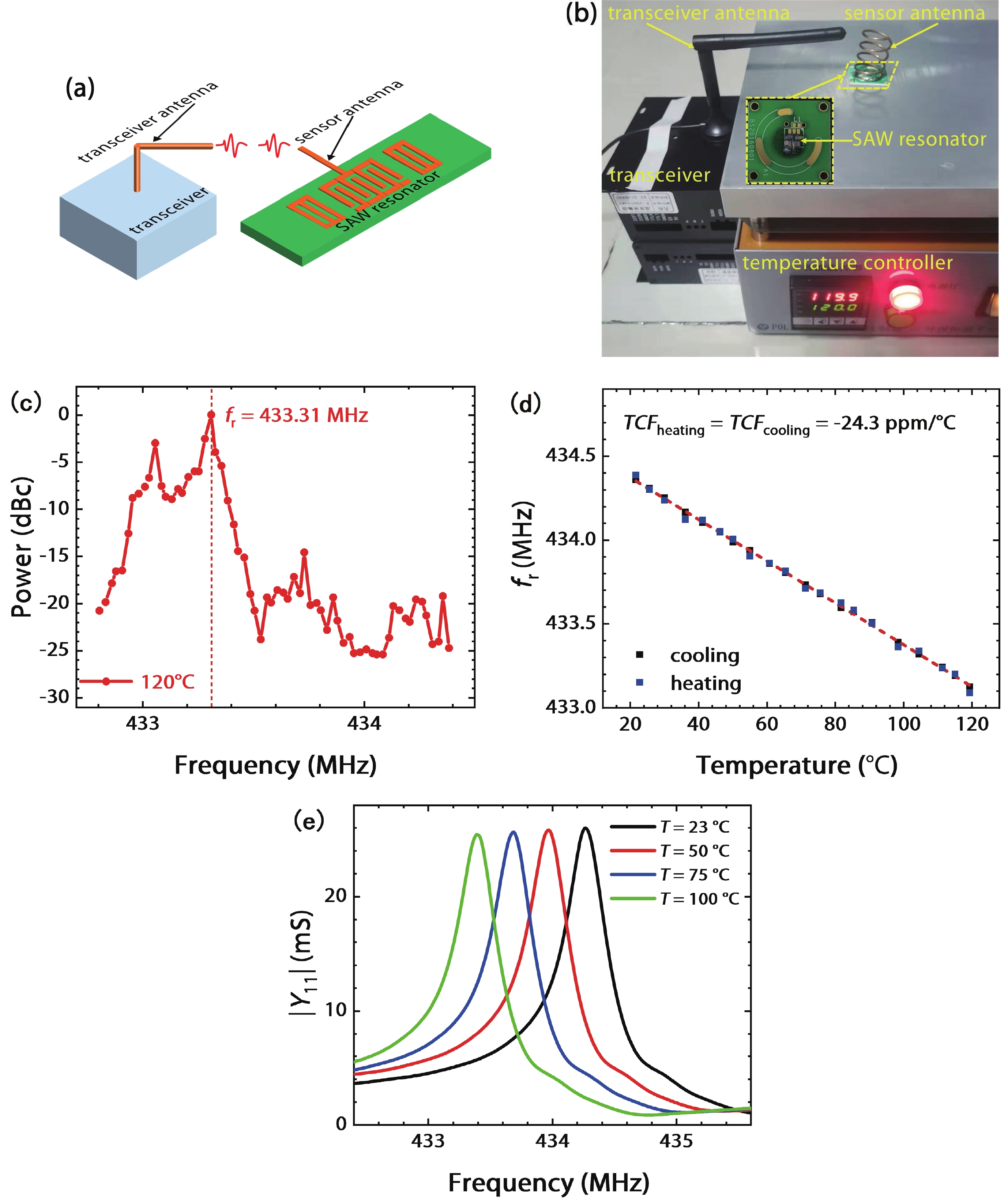
Surface acoustic wave (SAW) resonator with outstanding quality factors of 4829/6775 at the resonant/anti-resonant frequencies has been demonstrated on C-doped semi-insulating bulk GaN. The impact of device parameters including aspect ratio of length to width of resonators, number of interdigital transducers, and acoustic propagation direction on resonator performance have been studied. For the first time, we demonstrate wireless temperature sensing from 21.6 to 120 °C with a stable temperature coefficient of frequency of –24.3 ppm/°C on bulk GaN-based SAW resonators.
J. Semicond.
2022, 43(11): 112201 doi: 10.1088/1674-4926/43/11/112201
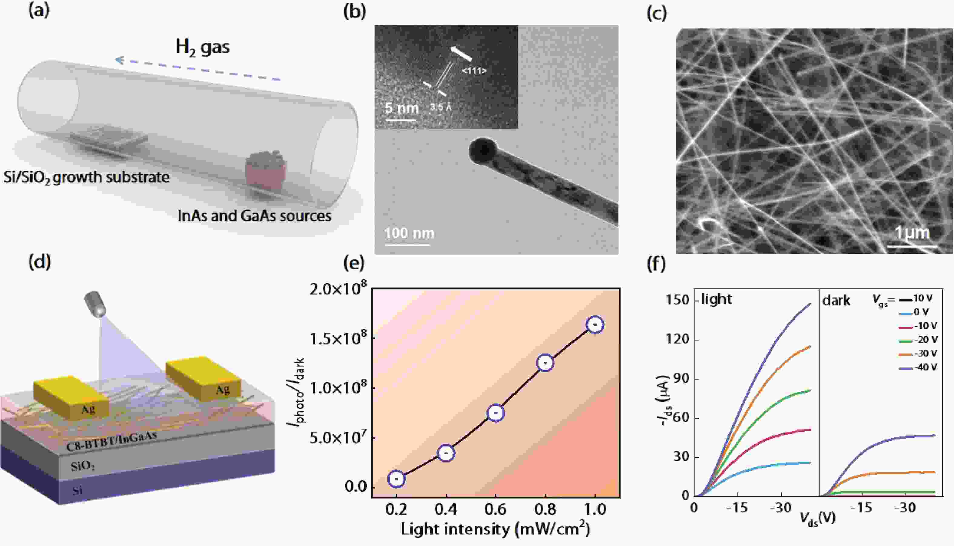
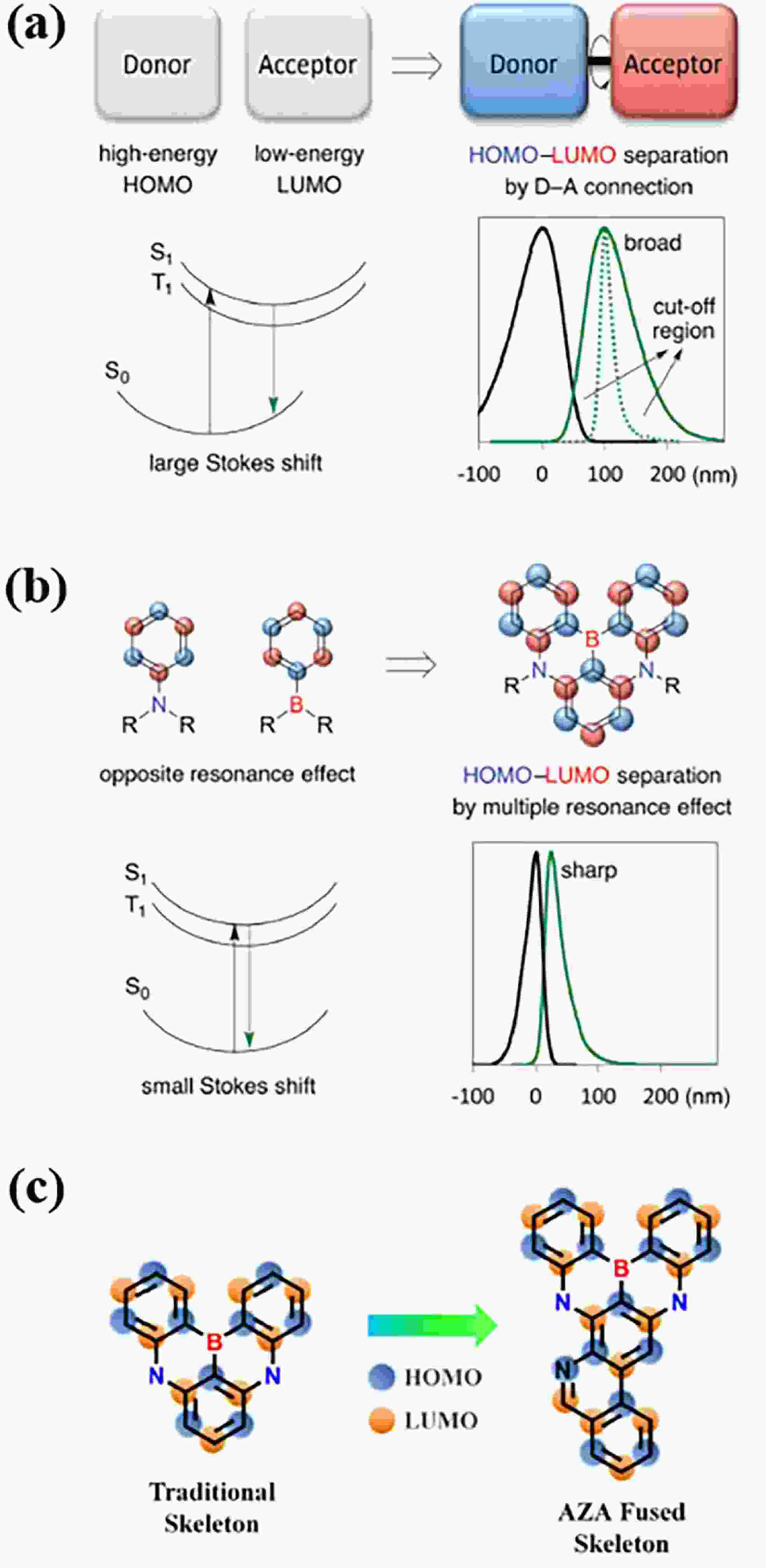
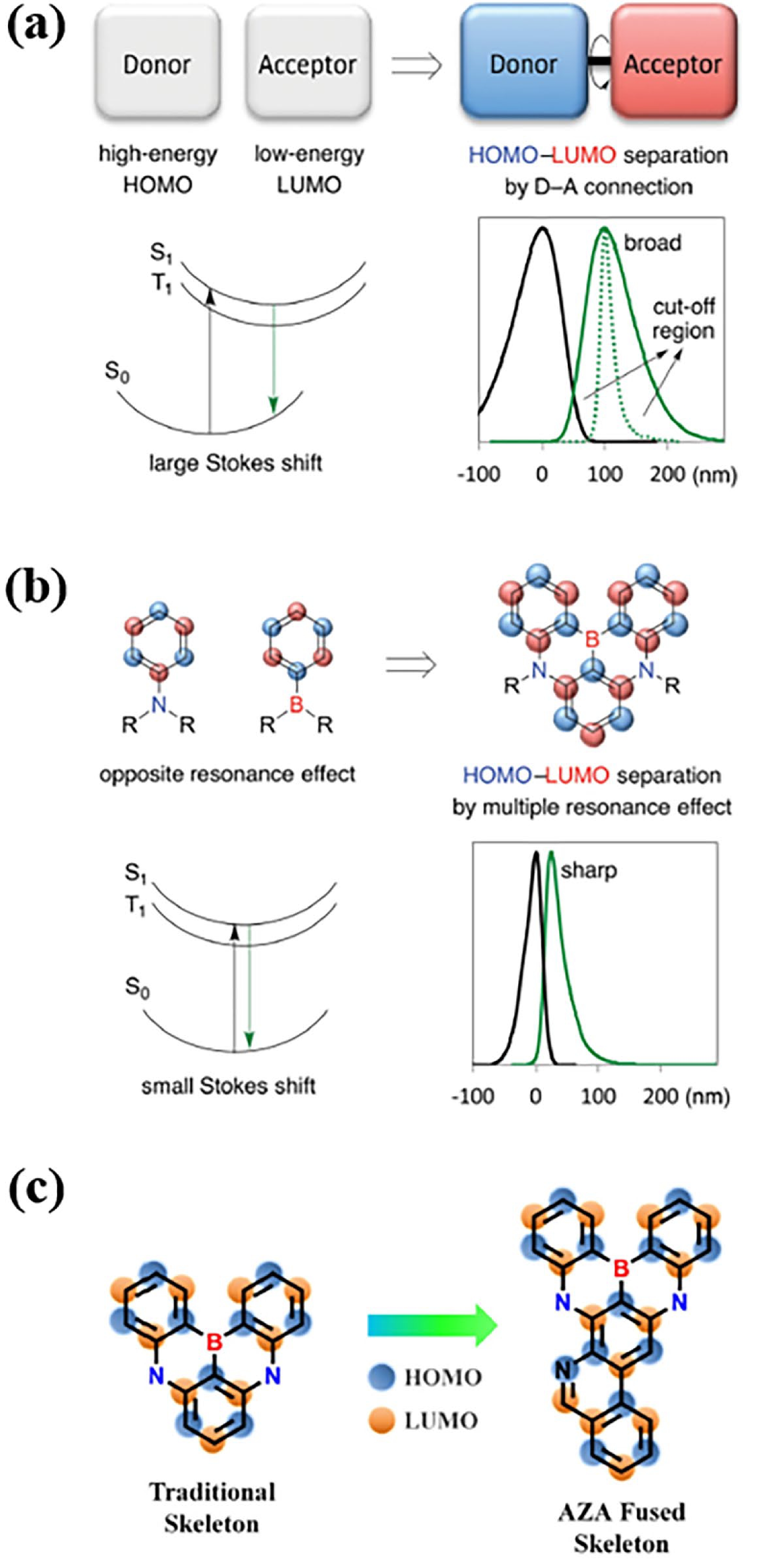
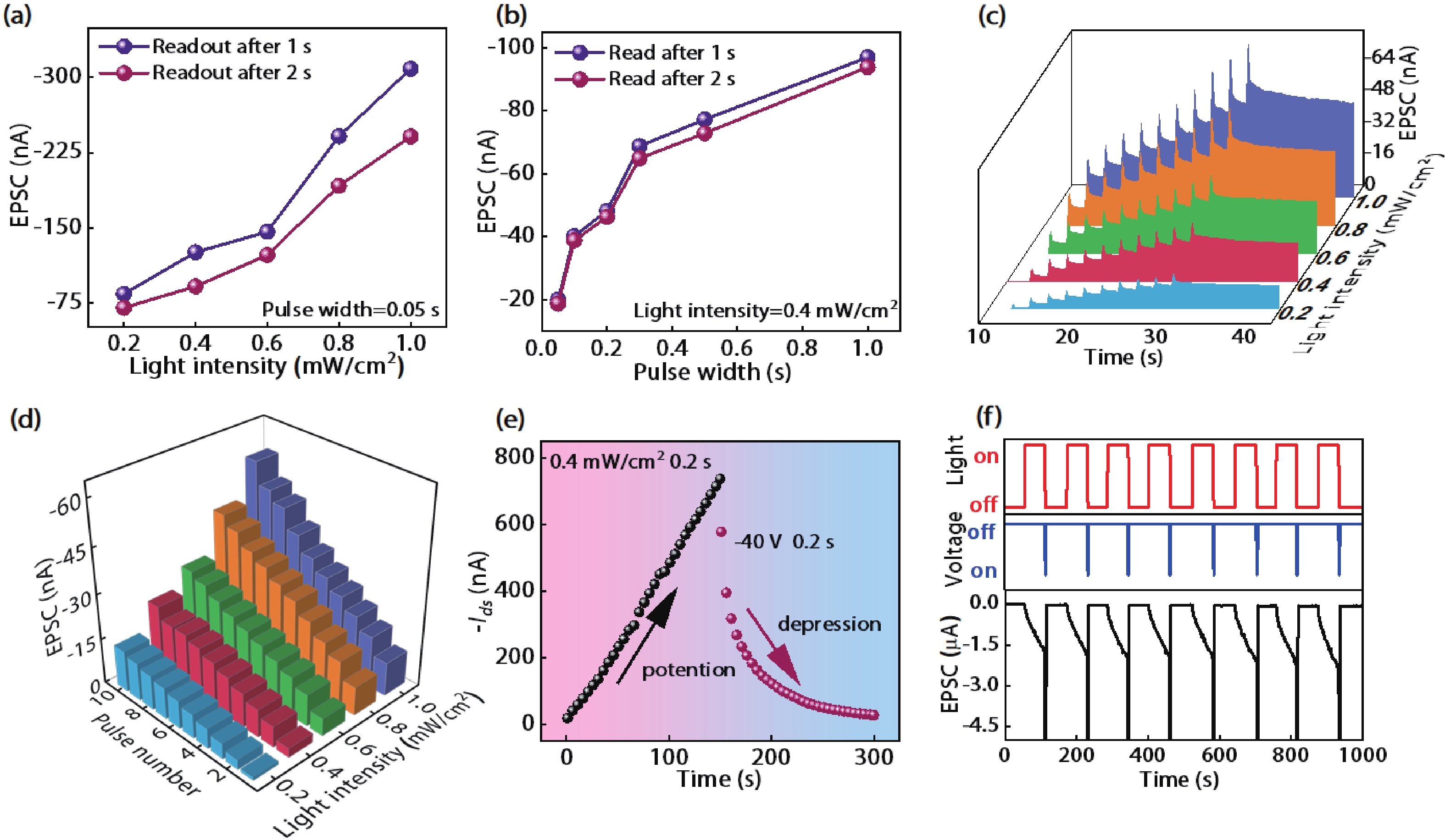
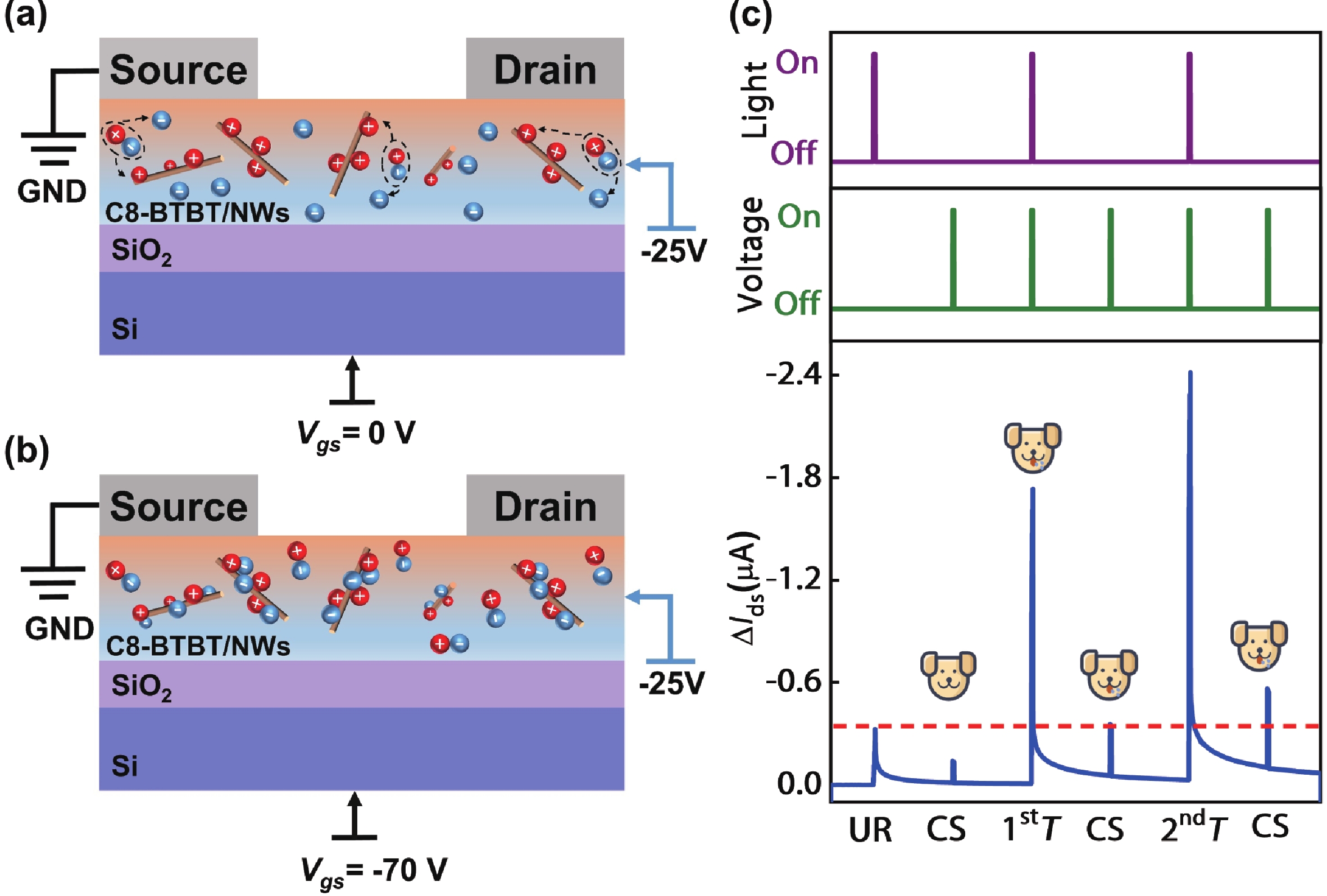
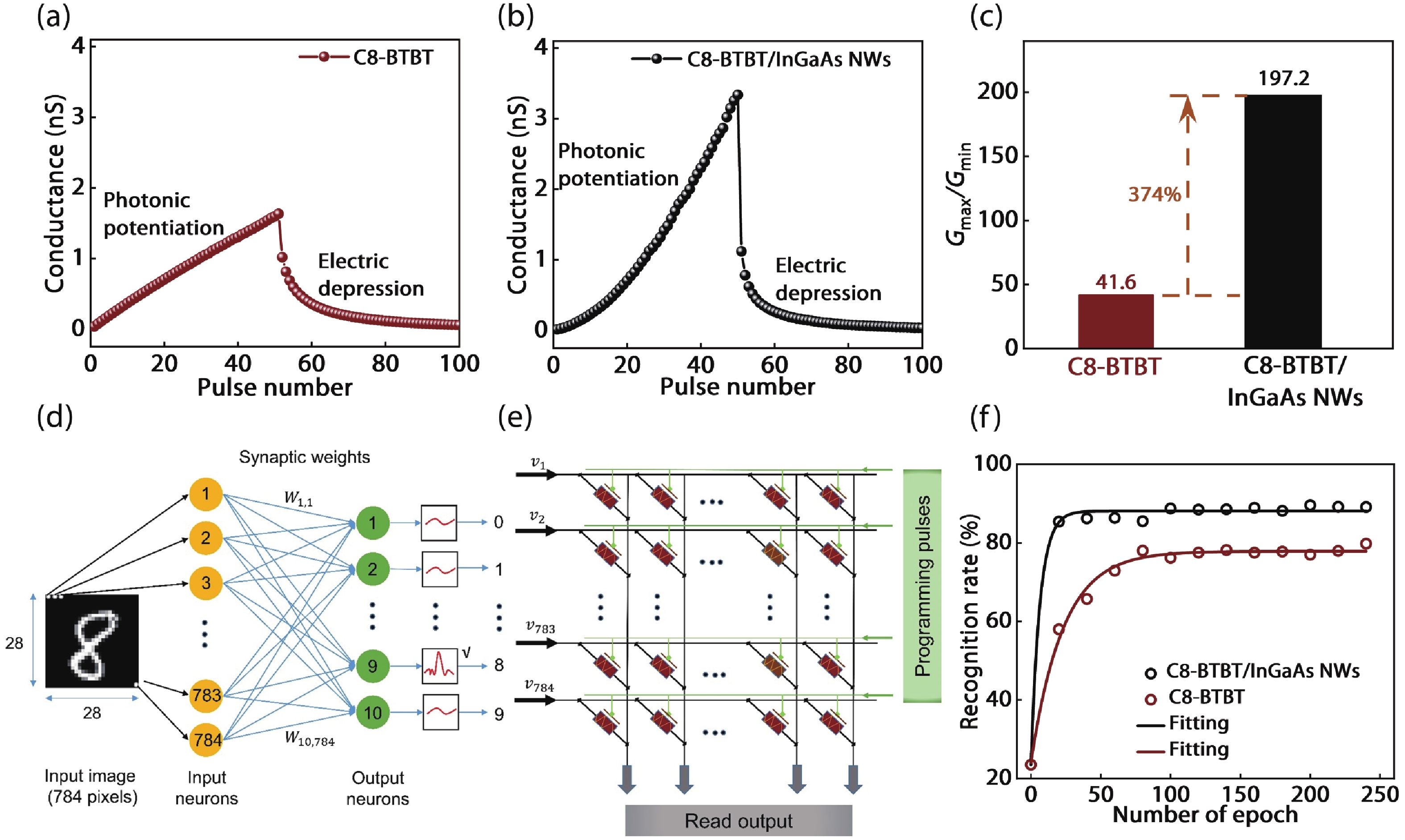
The emergence of light-tunable synaptic transistors provides opportunities to break through the von Neumann bottleneck and enable neuromorphic computing. Herein, a multifunctional synaptic transistor is constructed by using 2,7-dioctyl[1]benzothieno[3,2-b][1]benzothiophene (C8-BTBT) and indium gallium arsenide (InGaAs) nanowires (NWs) hybrid heterojunction thin film as the active layer. Under illumination, the Type-I C8-BTBT/InGaAs NWs heterojunction would make the dissociated photogenerated excitons more difficult to recombine. The persistent photoconductivity caused by charge trapping can then be used to mimic photosynaptic behaviors, including excitatory postsynaptic current, long/short-term memory and Pavlovian learning. Furthermore, a high classification accuracy of 89.72% can be achieved through the single-layer-perceptron hardware-based neural network built from C8-BTBT/InGaAs NWs synaptic transistors. Thus, this work could provide new insights into the fabrication of high-performance optoelectronic synaptic devices.


J. Semicond.
2022, 43(11): 112302 doi: 10.1088/1674-4926/43/11/112302
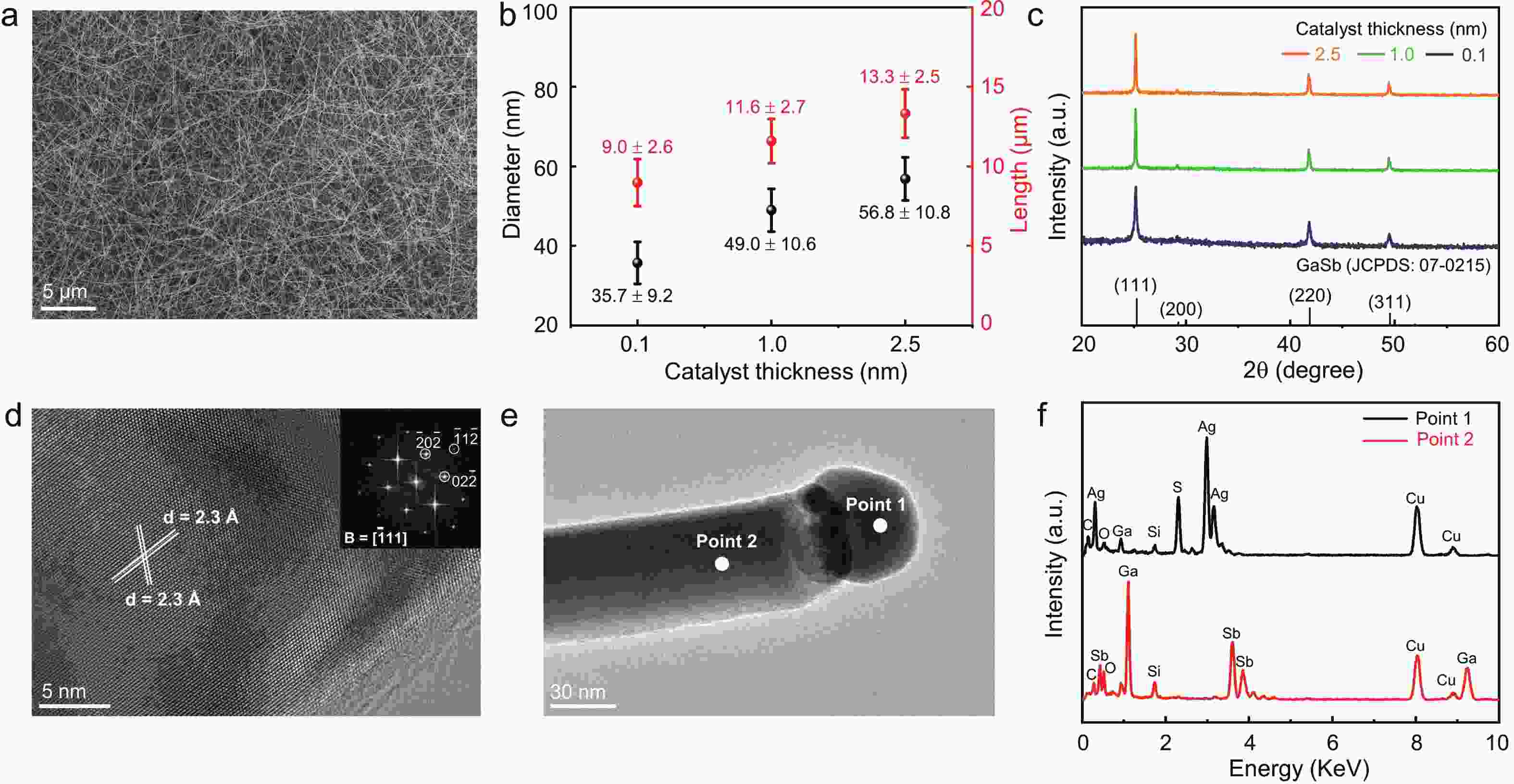
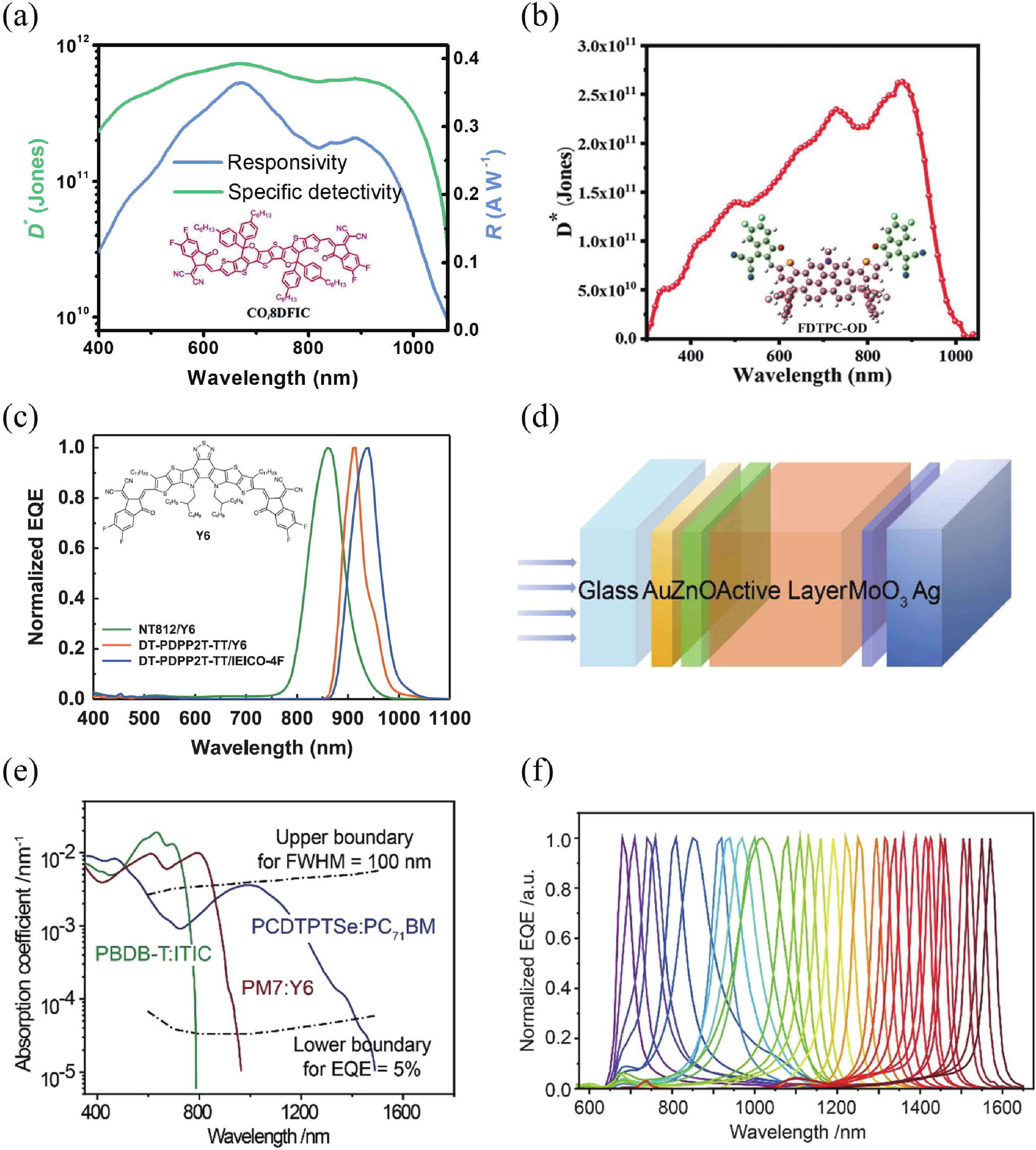
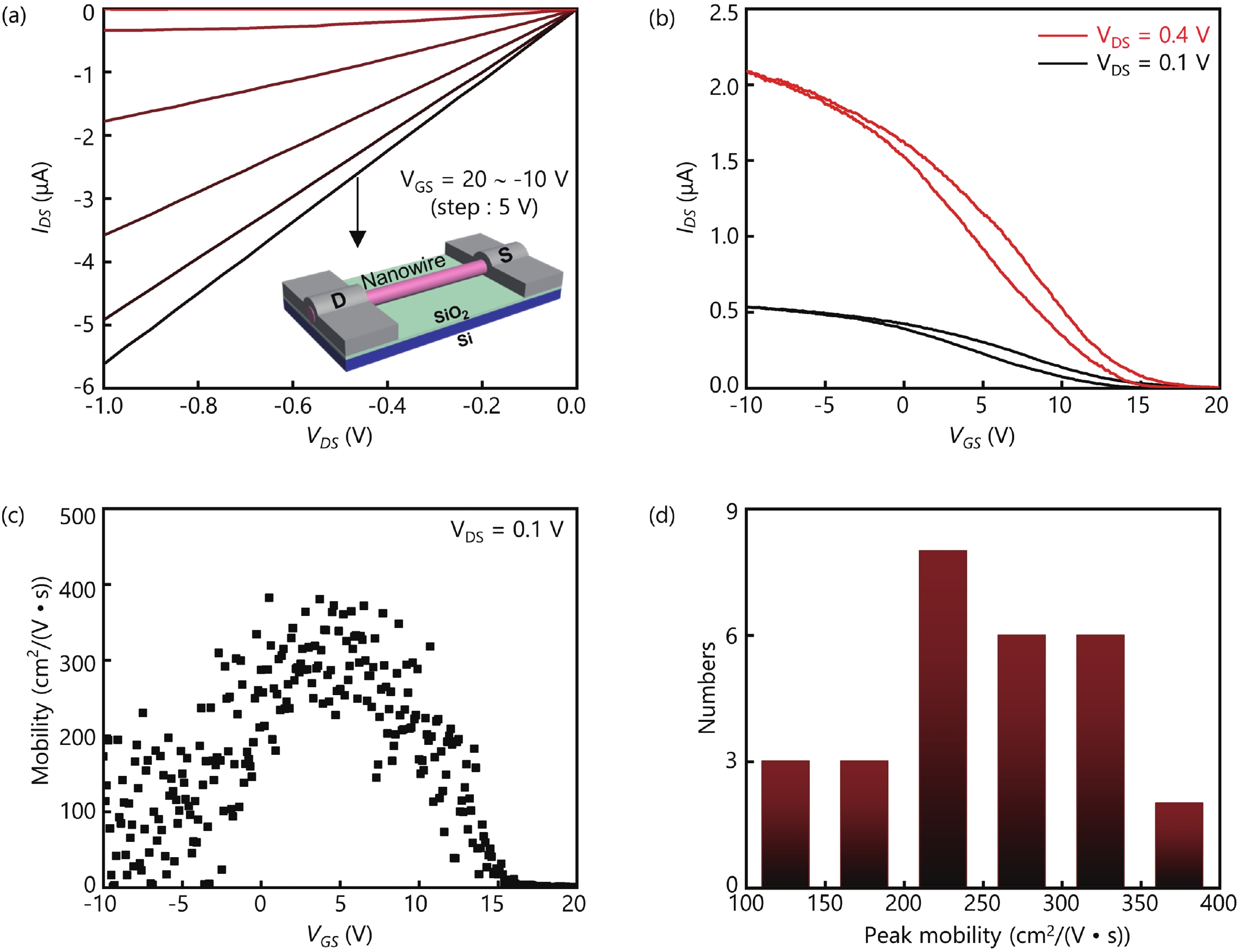
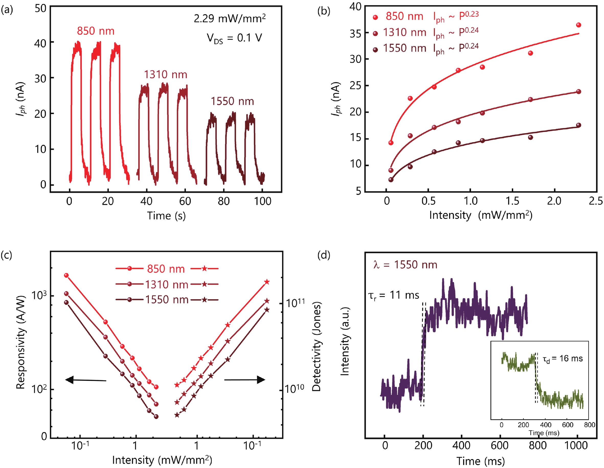
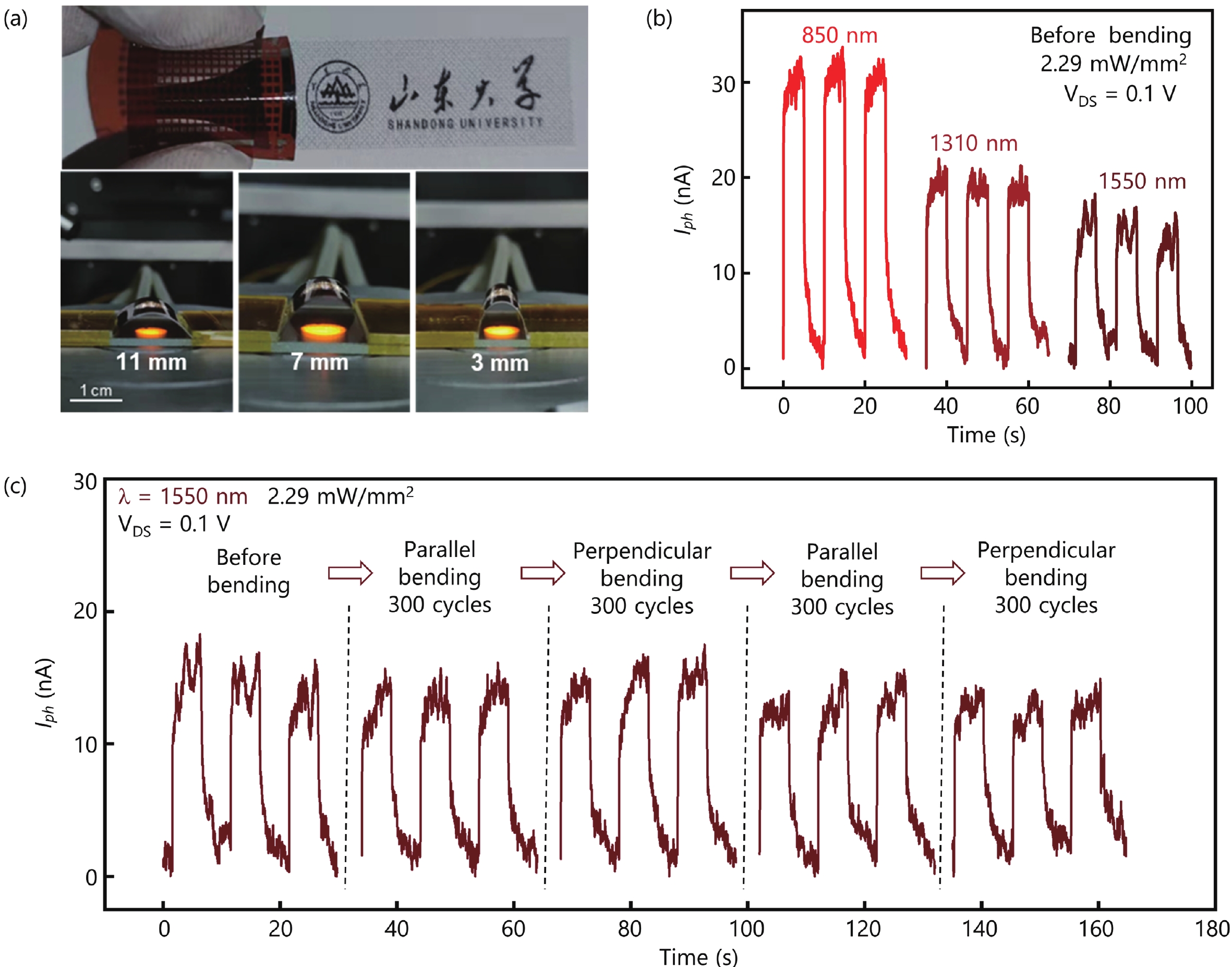
High-quality narrow bandgap semiconductors nanowires (NWs) challenge the flexible near-infrared (NIR) photodetectors in next-generation imaging, data communication, environmental monitoring, and bioimaging applications. In this work, complementary metal oxide semiconductor-compatible metal of Ag is deposited on glass as the growth catalyst for the surfactant-assisted chemical vapor deposition of GaSb NWs. The uniform morphology, balance stoichiometry, high-quality crystallinity, and phase purity of as-prepared NWs are checked by scanning electron microscopy, energy dispersive X-ray spectroscopy, high-resolution transmission electron microscopy, and X-ray diffraction. The electrical properties of as-prepared NWs are studied by constructing back-gated field-effect-transistors, displaying a high Ion/Ioff ratio of 104 and high peak hole mobility of 400 cm2/(V·s). Benefiting from the excellent electrical and mechanical flexibility properties, the as-fabricated NW flexible NIR photodetector exhibits high sensitivity and excellent photoresponse, with responsivity as high as 618 A/W and detectivity as high as 6.7 × 10¹⁰ Jones. Furthermore, there is no obvious decline in NIR photodetection behavior, even after parallel and perpendicular folding with 1200 cycles.

J. Semicond.
2022, 43(11): 112502 doi: 10.1088/1674-4926/43/11/112502
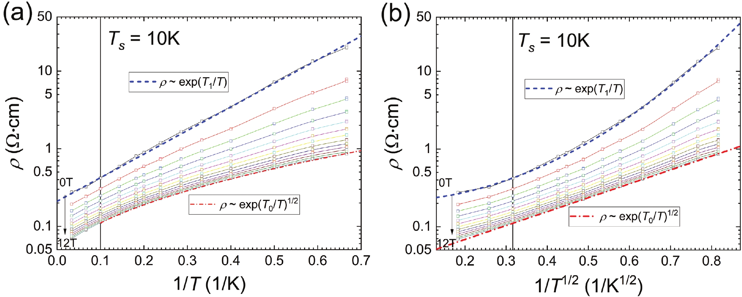
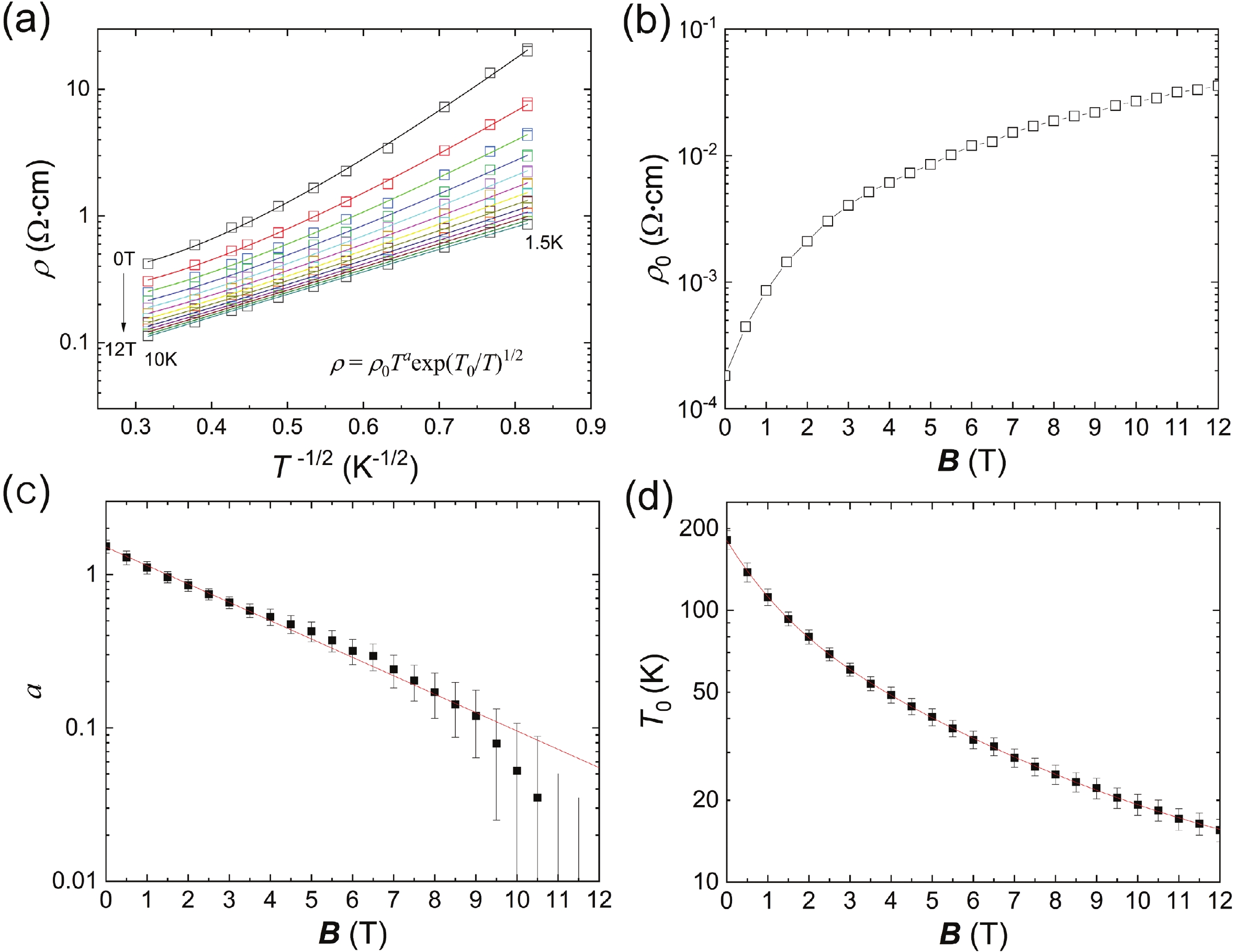
Ferromagnetic semiconductor Ga1–xMnxAs1–yPy thin films go through a metal–insulator transition at low temperature where electrical conduction becomes driven by hopping of charge carriers. In this regime, we report a colossal negative magnetoresistance (CNMR) coexisting with a saturated magnetic moment, unlike in the traditional magnetic semiconductor Ga1–xMnxAs. By analyzing the temperature dependence of the resistivity at fixed magnetic field, we demonstrate that the CNMR can be consistently described by the field dependence of the localization length, which relates to a field dependent mobility edge. This dependence is likely due to the random environment of Mn atoms in Ga1–xMnxAs1–yPy which causes a random spatial distribution of the mobility that is suppressed by an increasing magnetic field.