Issue Browser
Volume 42, Issue 5,
May 2021


J. Semicond.
2021, 42(5): 051001 doi: 10.1088/1674-4926/42/5/051001
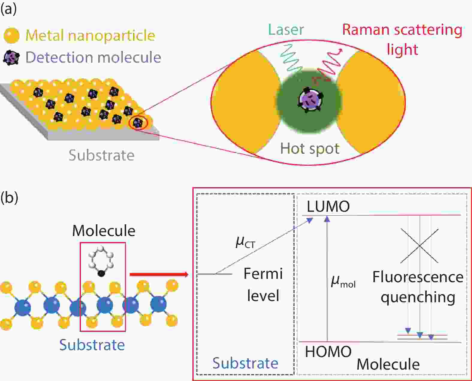
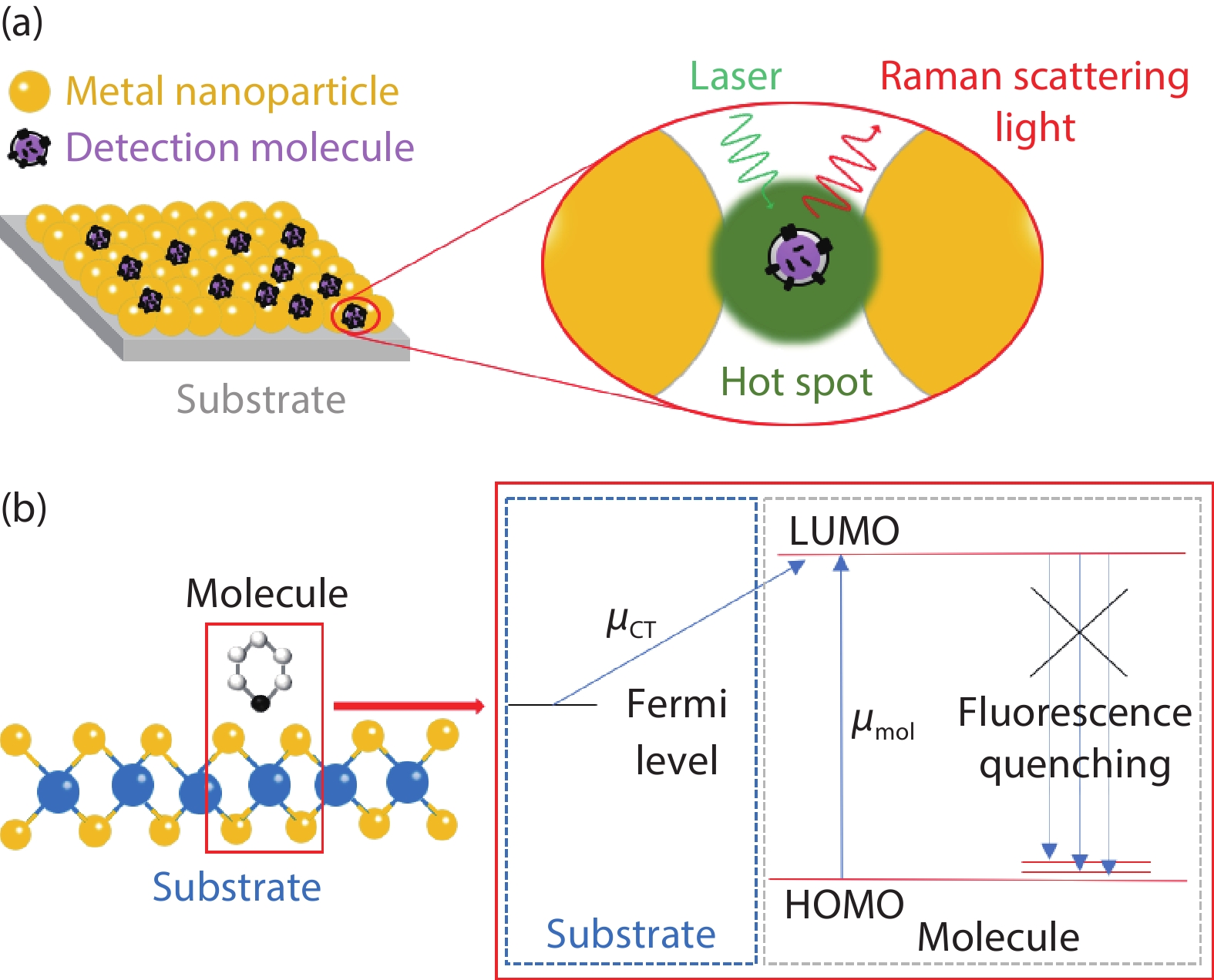
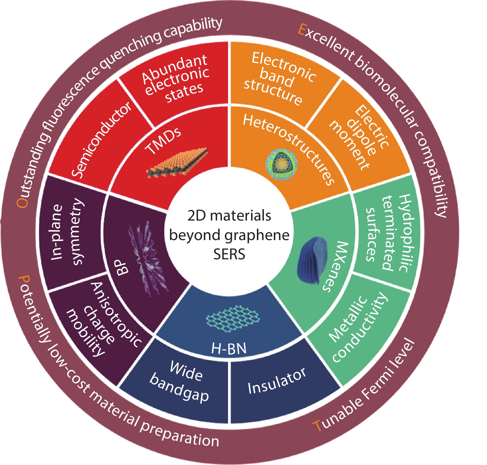
Surface-enhanced Raman spectroscopy (SERS) based on two-dimensional (2D) materials has attracted great attention over the past decade. Compared with metallic materials, which enhance Raman signals via the surface plasmon effect, 2D materials integrated on silicon substrates are ideal for use in the fabrication of plasmon-free SERS chips, with the advantages of outstanding fluorescence quenching capability, excellent biomolecular compatibility, tunable Fermi levels, and potentially low-cost material preparation. Moreover, recent studies have shown that the limits of detection of 2D-material-based SERS may be comparable with those of metallic substrates, which has aroused significant research interest. In this review, we comprehensively summarize the advances in SERS chips based on 2D materials. As several excellent reviews of graphene-enhanced Raman spectroscopy have been published in the past decade, here, we focus only on 2D materials beyond graphene, i.e., transition metal dichalcogenides, black phosphorus, hexagonal boron nitride, 2D titanium carbide or nitride, and their heterostructures. We hope that this paper can serve as a useful reference for researchers specializing in 2D materials, spectroscopy, and diverse applications related to chemical and biological sensing.
J. Semicond.
2021, 42(5): 051801 doi: 10.1088/1674-4926/42/5/051801

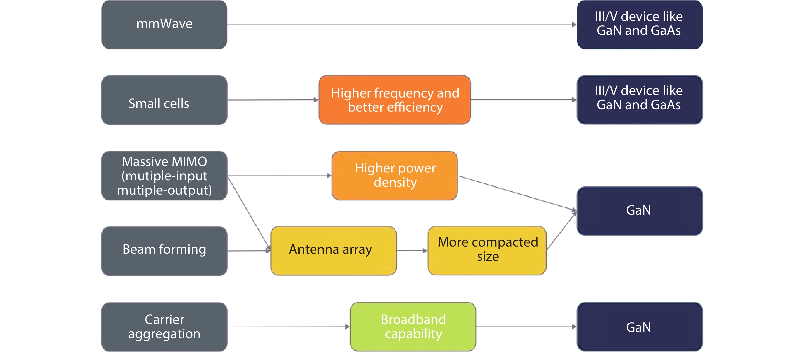
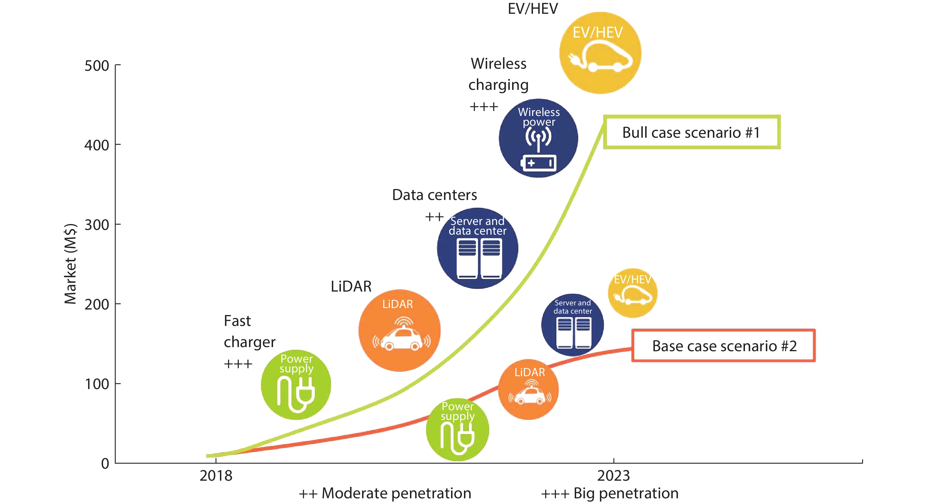
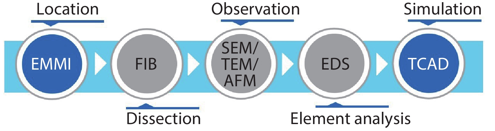
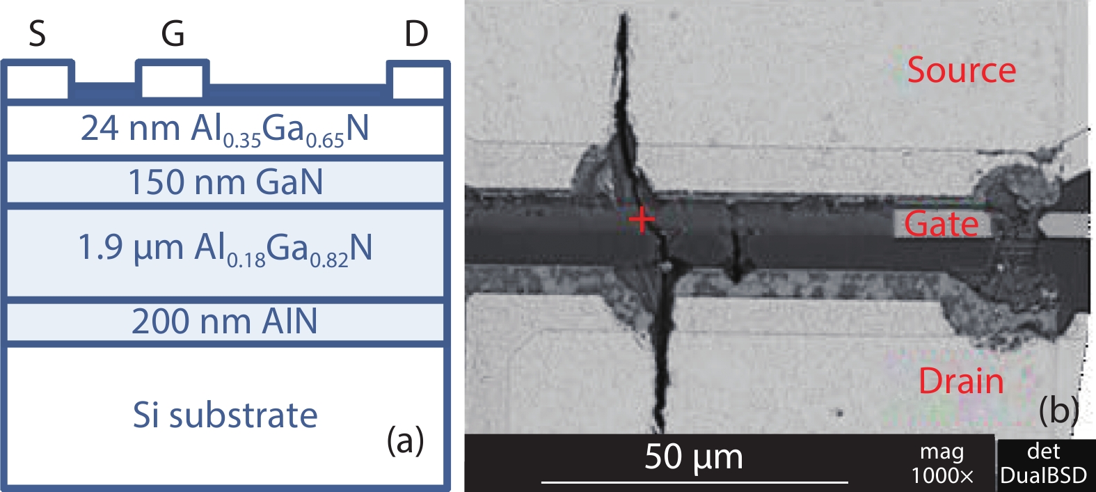
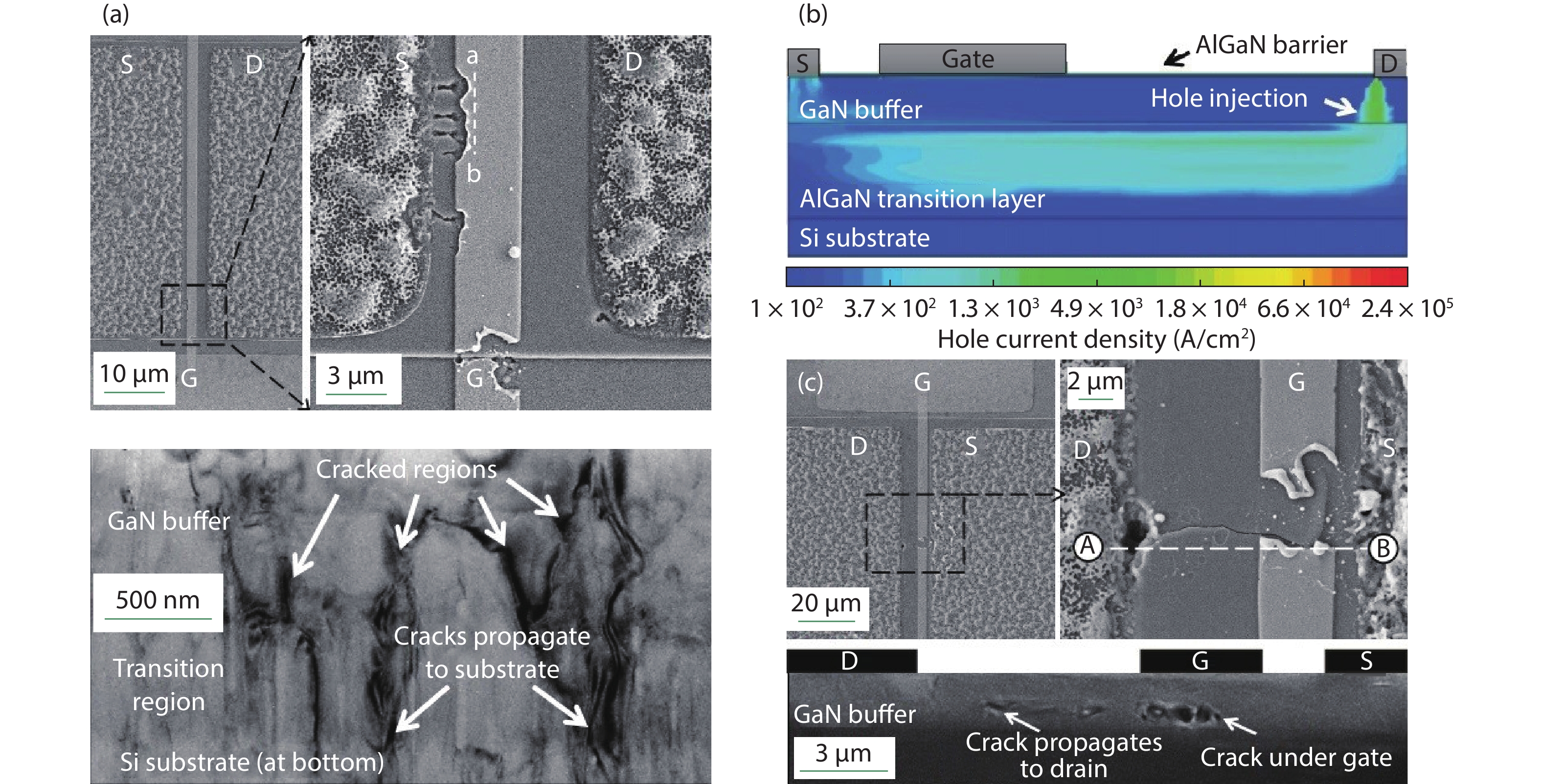
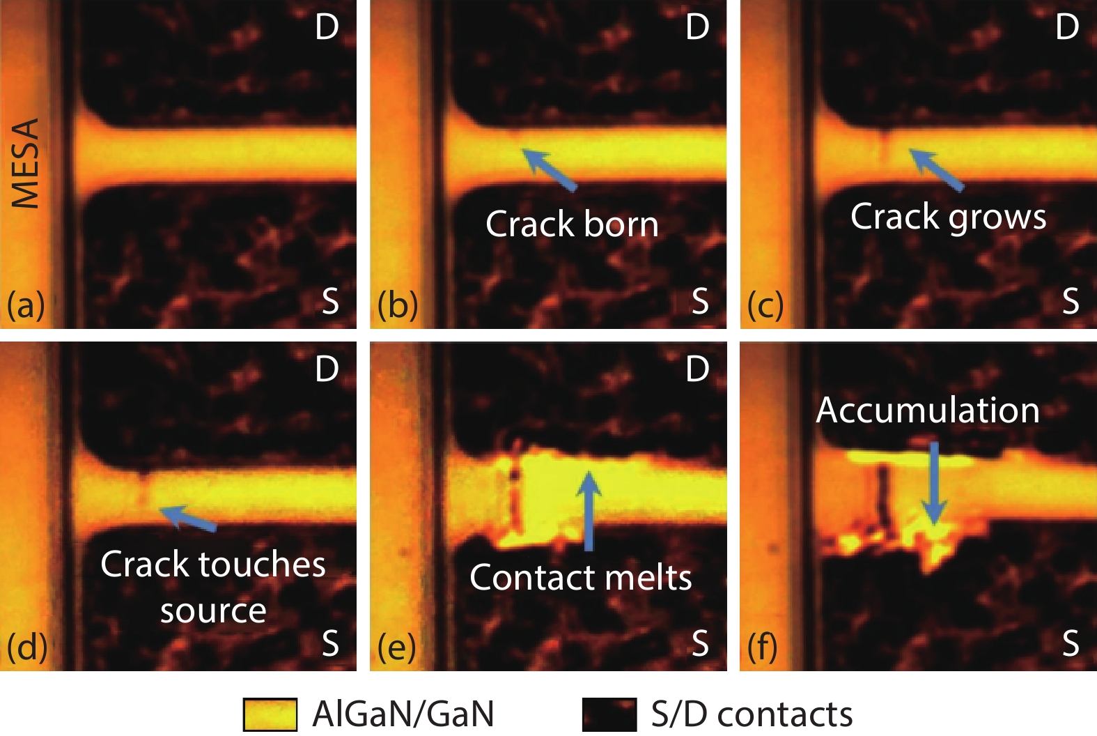
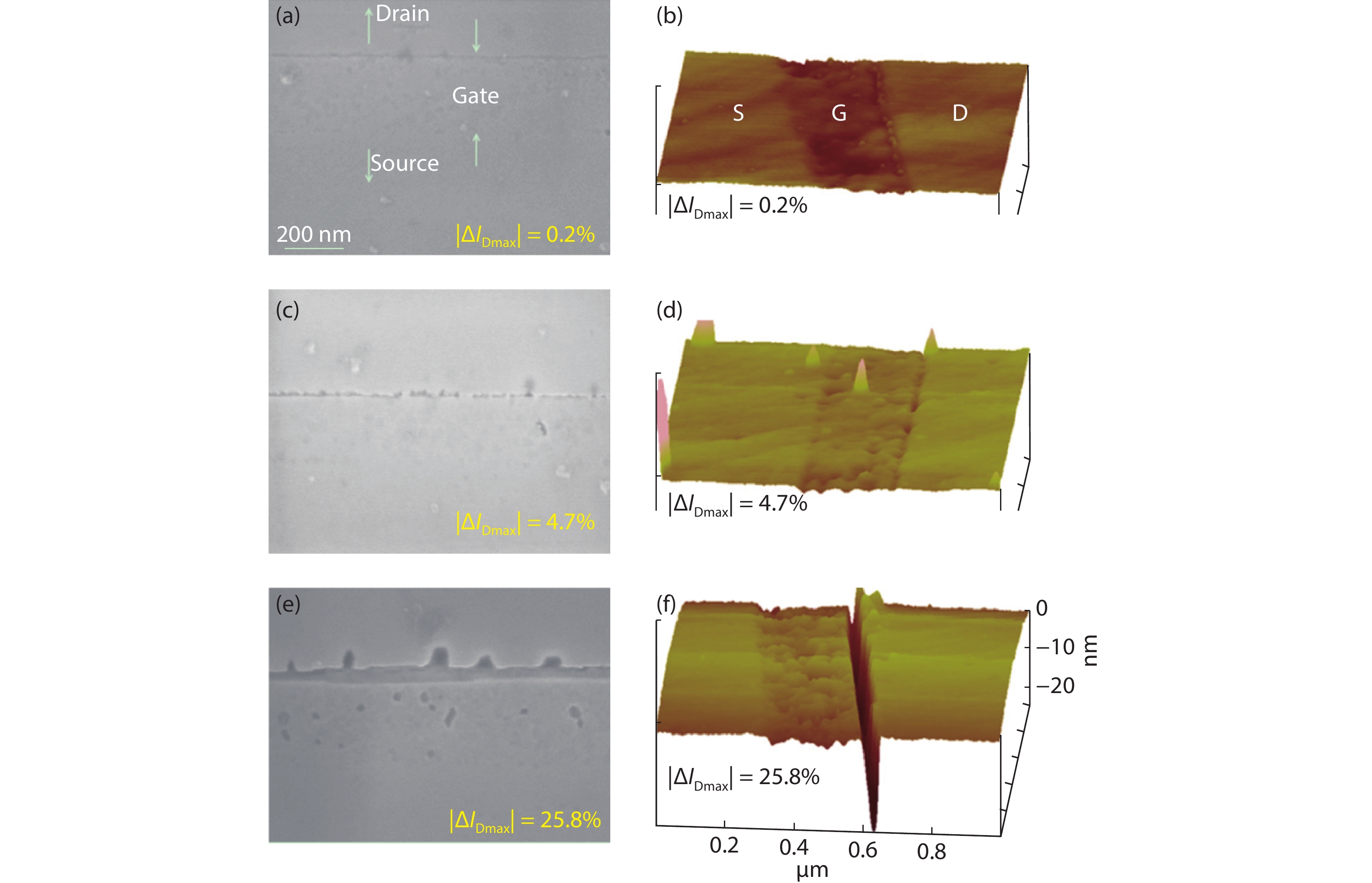
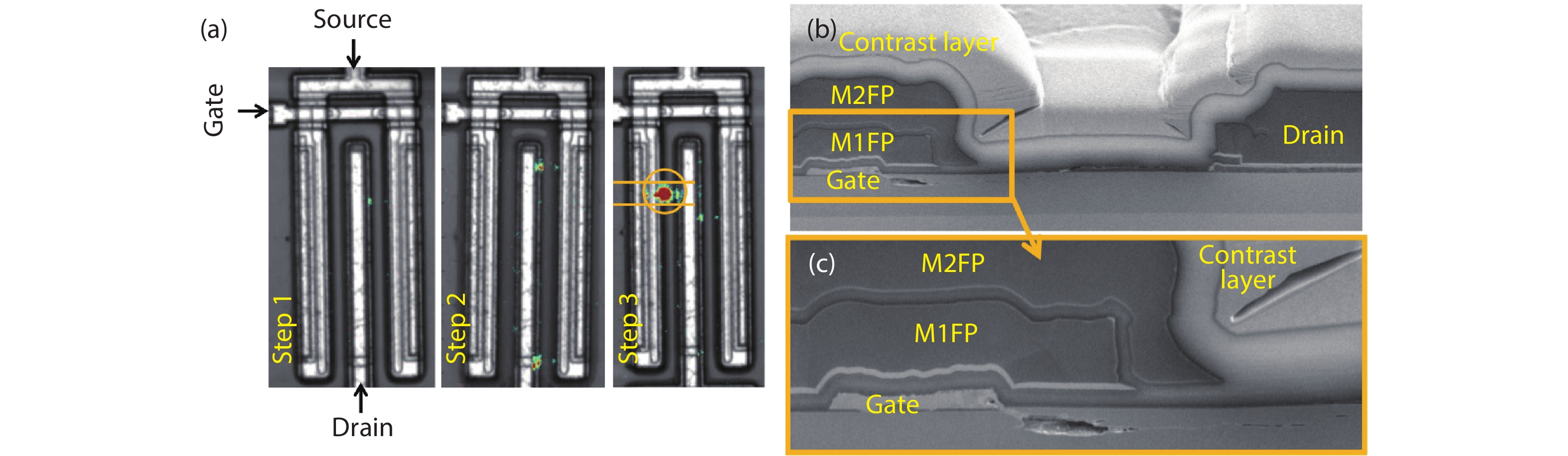
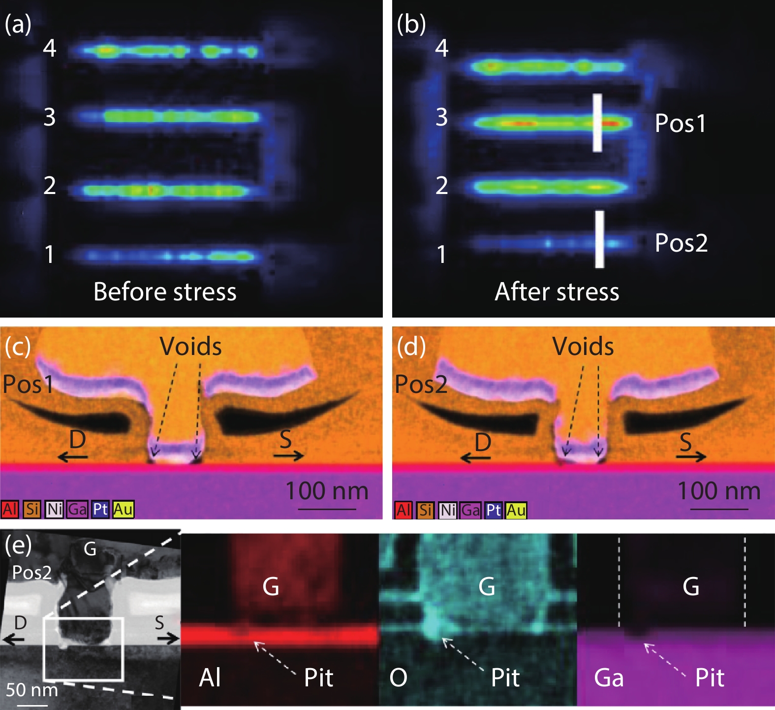
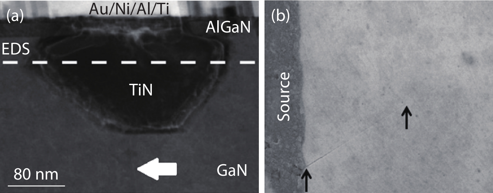
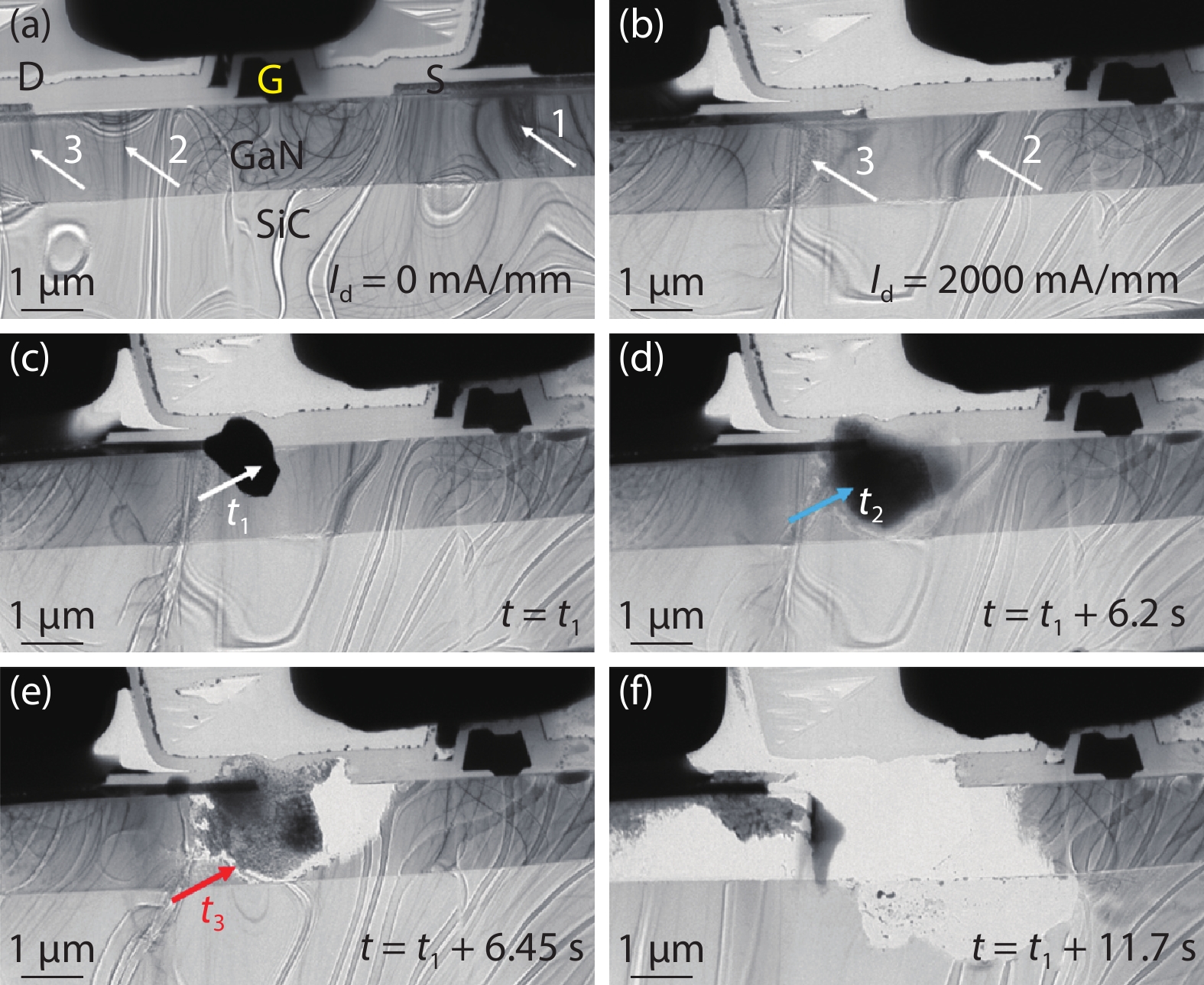
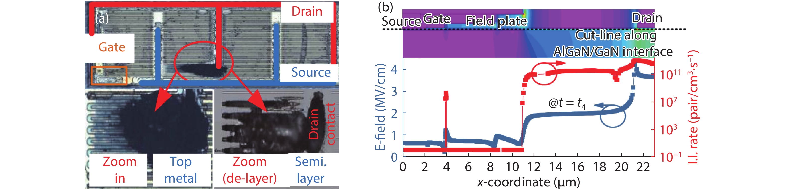
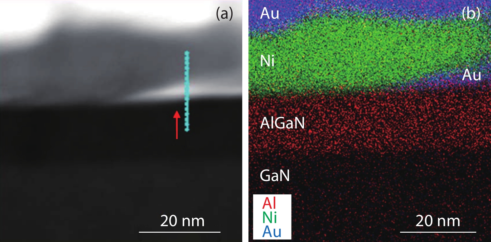
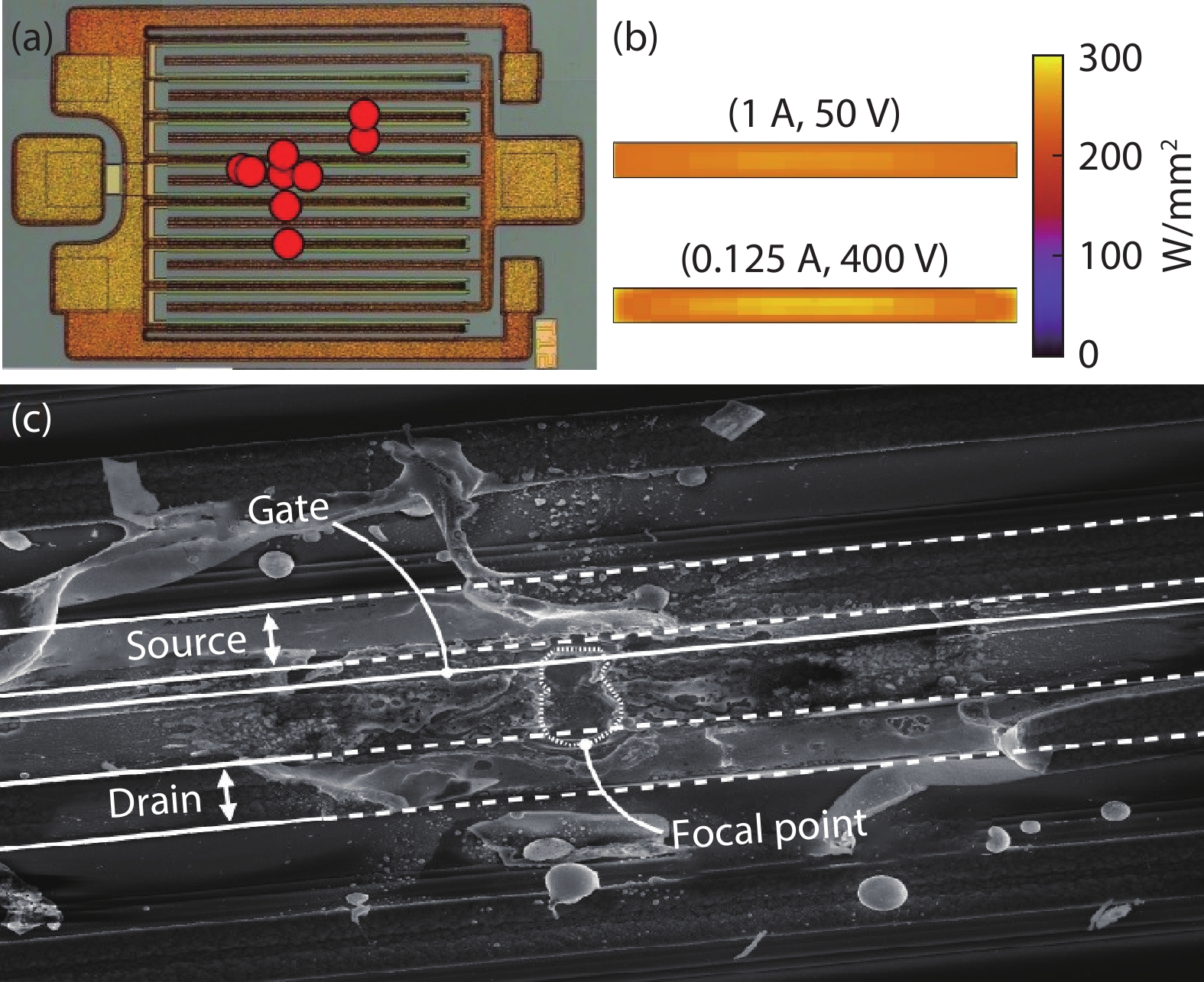
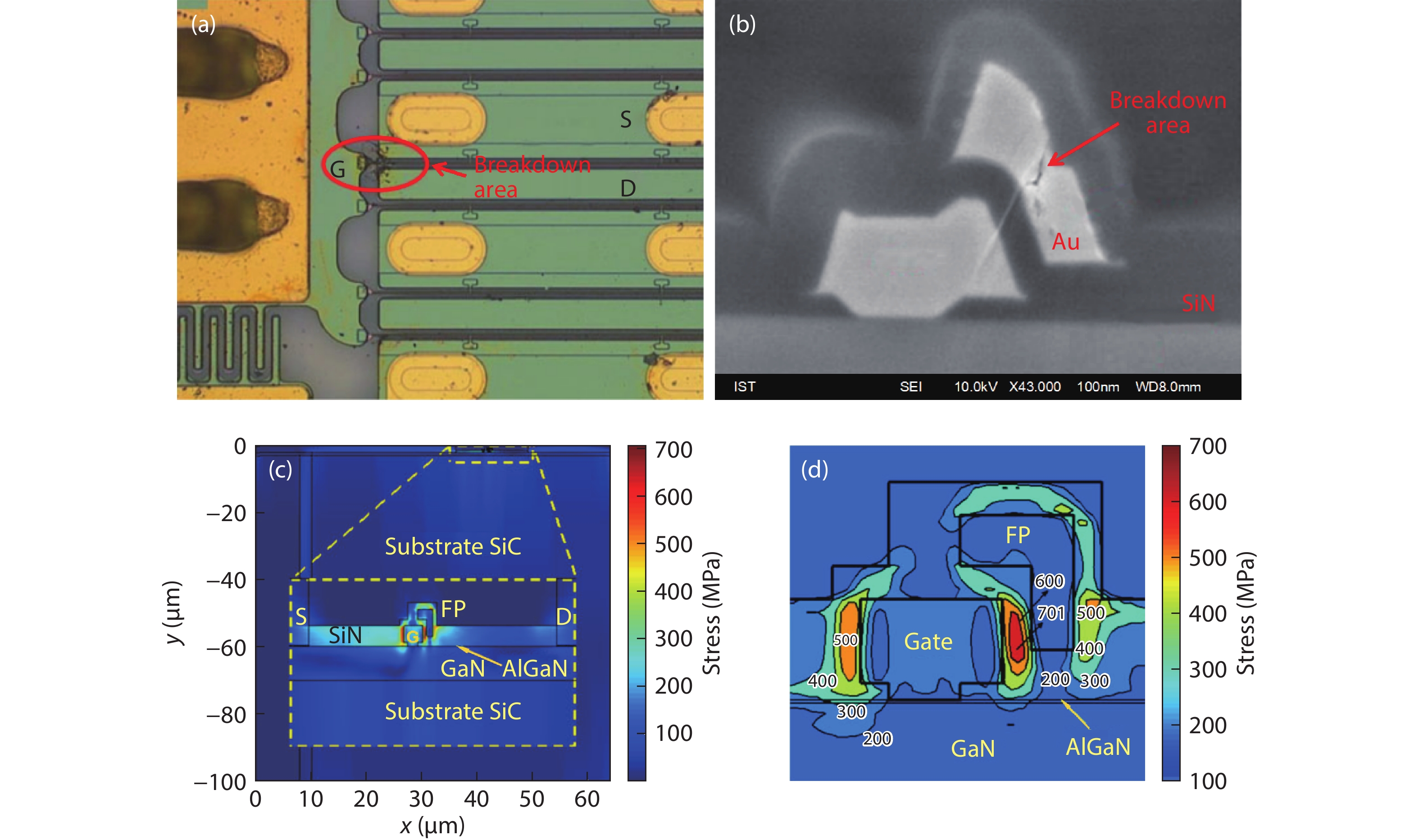
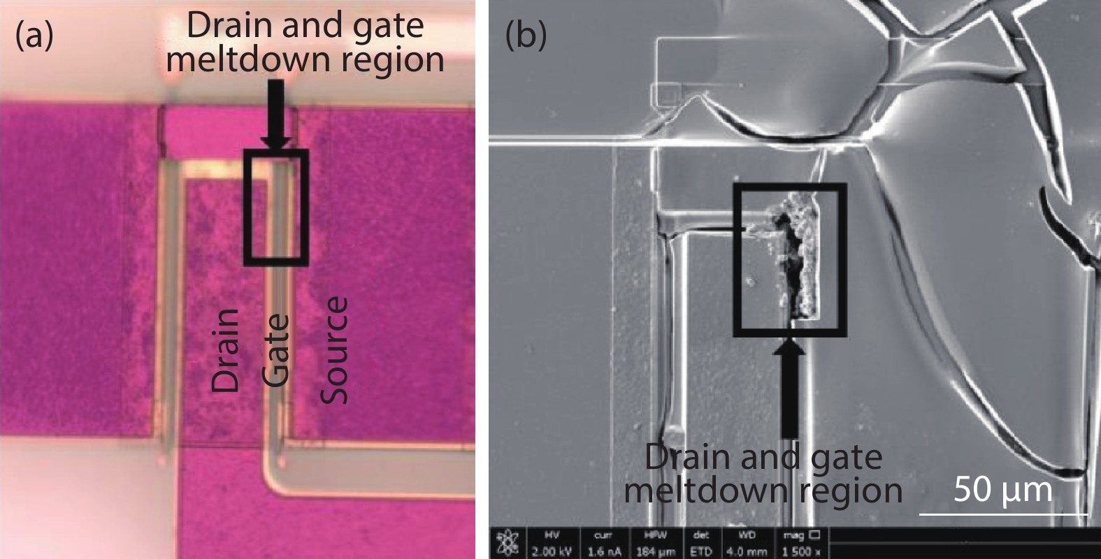
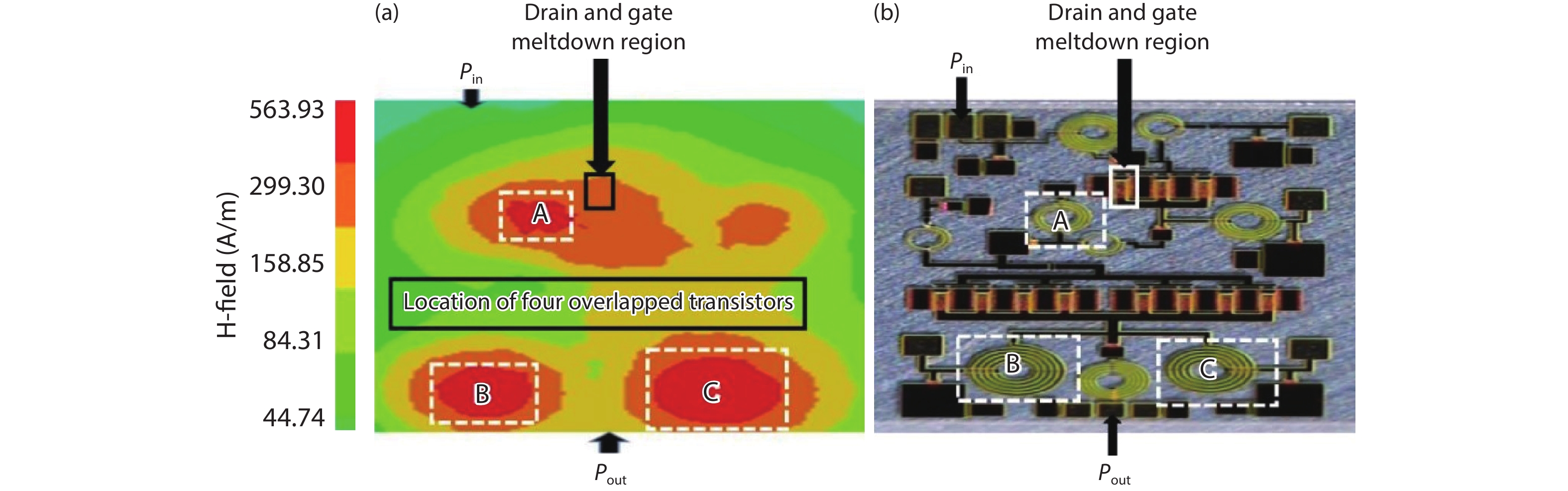
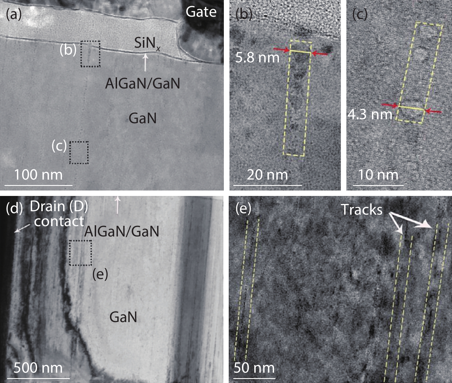
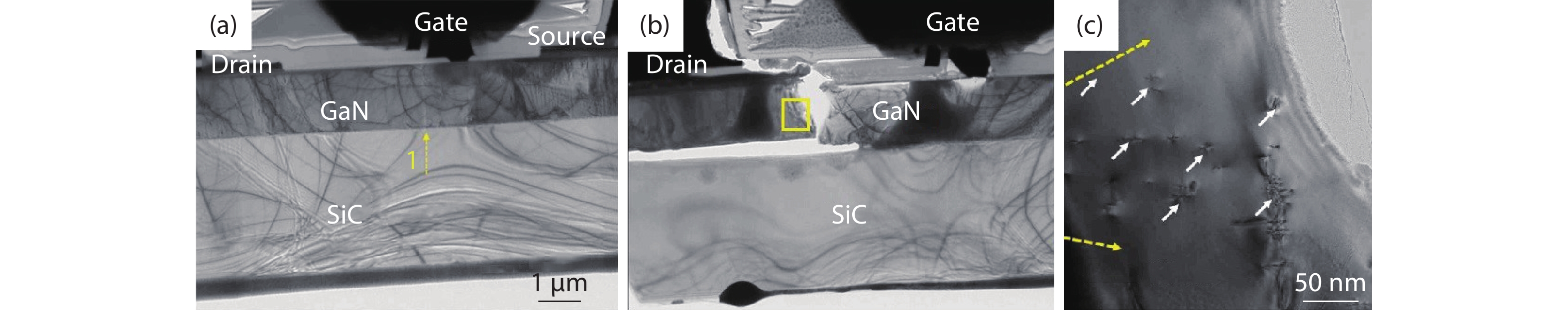
Gallium nitride (GaN)-based high-electron mobility transistors (HEMTs) are widely used in high power and high frequency application fields, due to the outstanding physical and chemical properties of the GaN material. However, GaN HEMTs suffer from degradations and even failures during practical applications, making physical analyses of post-failure devices extremely significant for reliability improvements and further device optimizations. In this paper, common physical characterization techniques for post failure analyses are introduced, several failure mechanisms and corresponding failure phenomena are reviewed and summarized, and finally device optimization methods are discussed.
J. Semicond.
2021, 42(5): 052001 doi: 10.1088/1674-4926/42/5/052001
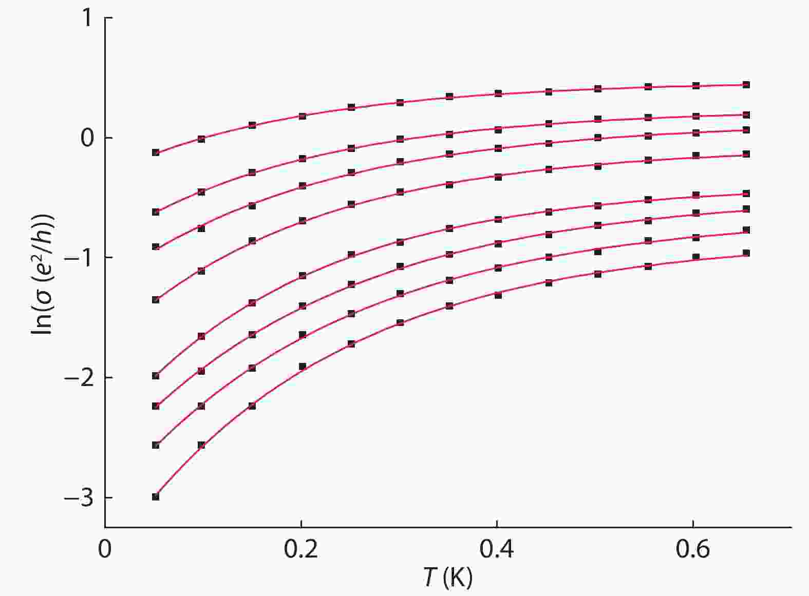
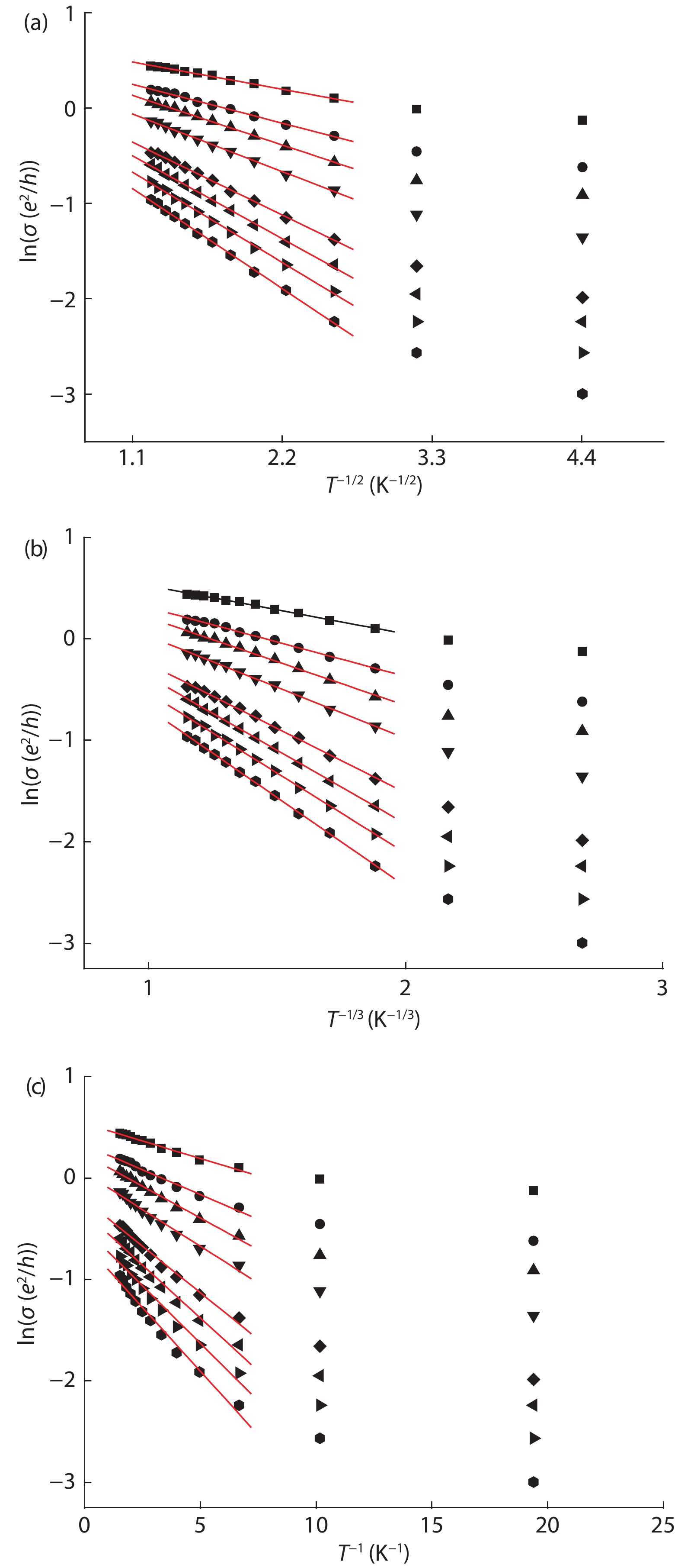
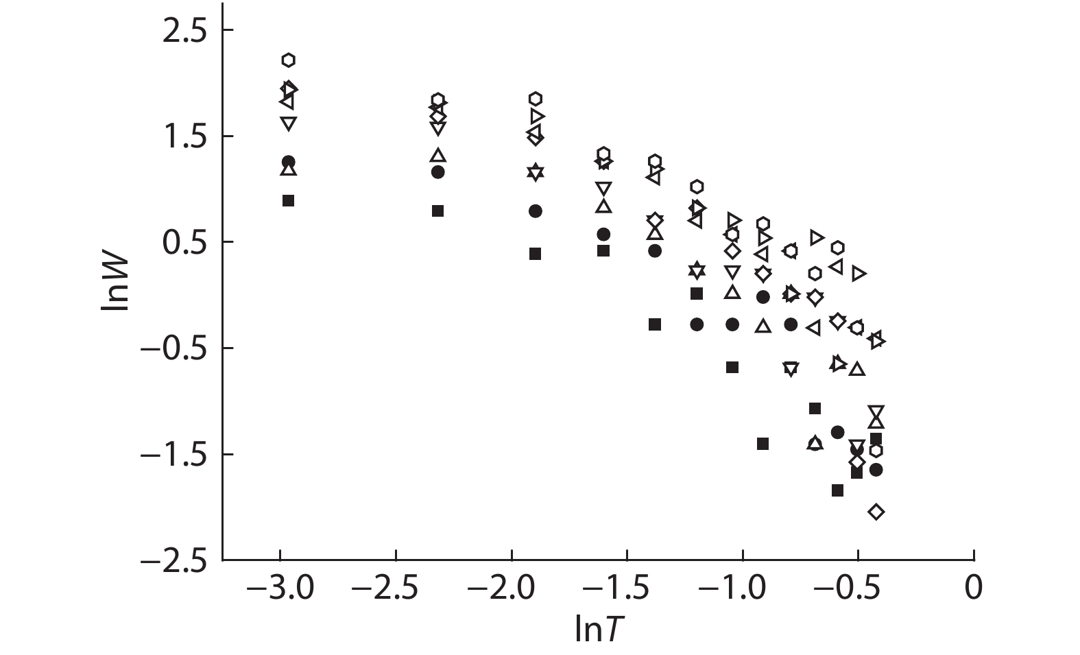
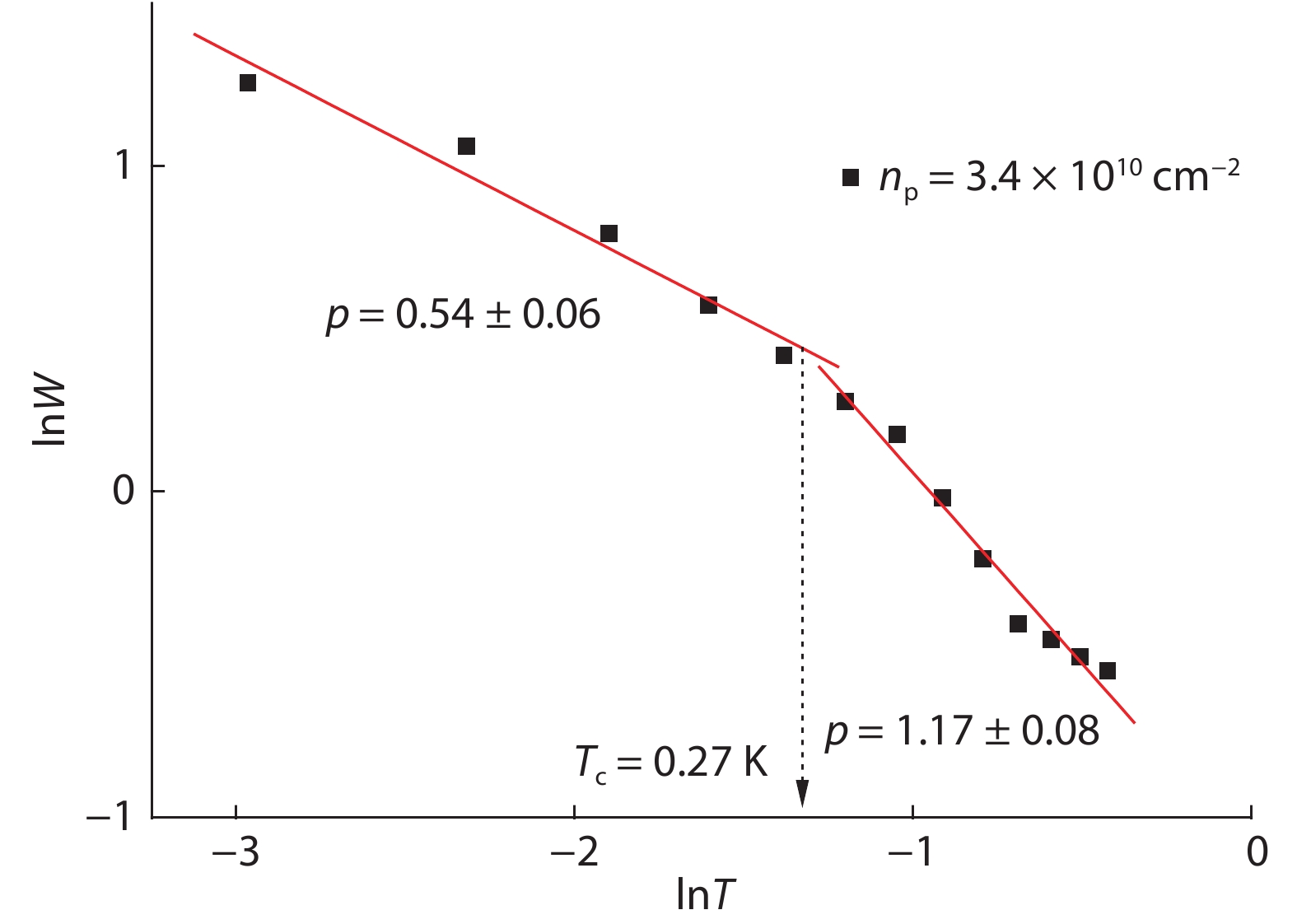
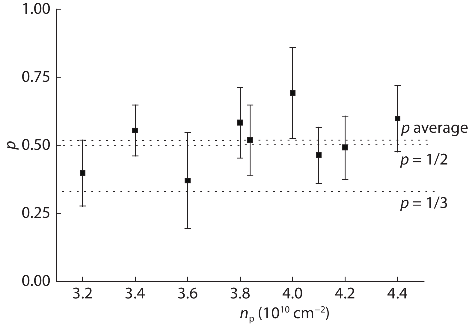
In this paper, we discuss low-temperature hopping-conductivity behavior in the insulating phase, in the absence of a magnetic field. We conduct a theoretical study of the crossover from hopping to activated transport in a GaAs two-dimensional hole system at low temperatures, finding that a crossover takes place from the Efros-Shklovskii variable-range hopping (VRH) regime to an activated regime in this system. This conductivity behavior in p-GaAs quantum wells is qualitatively consistent with the laws laid down in theories of localized electron interactions. Given sufficiently strong interactions, the holes in the localized states are able to hop collectively.


J. Semicond.
2021, 42(5): 052101 doi: 10.1088/1674-4926/42/5/052101
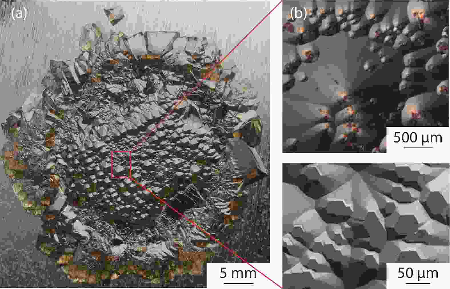
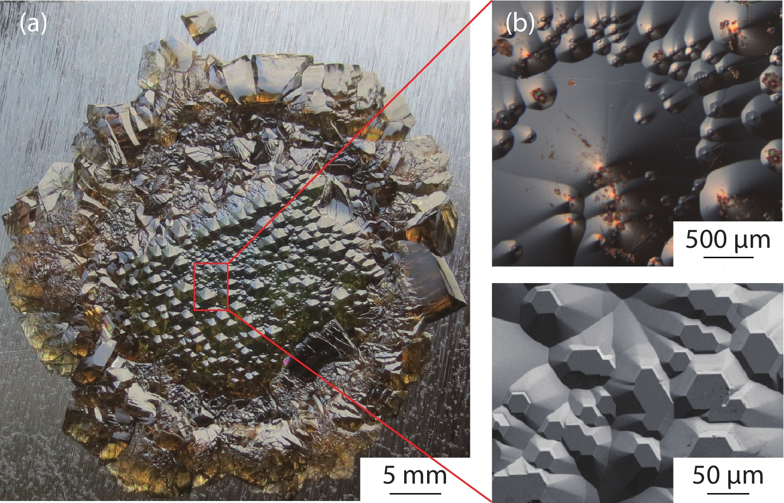
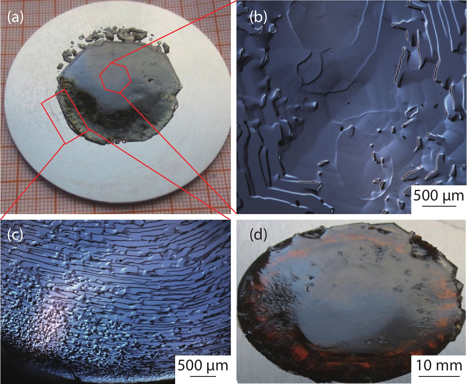
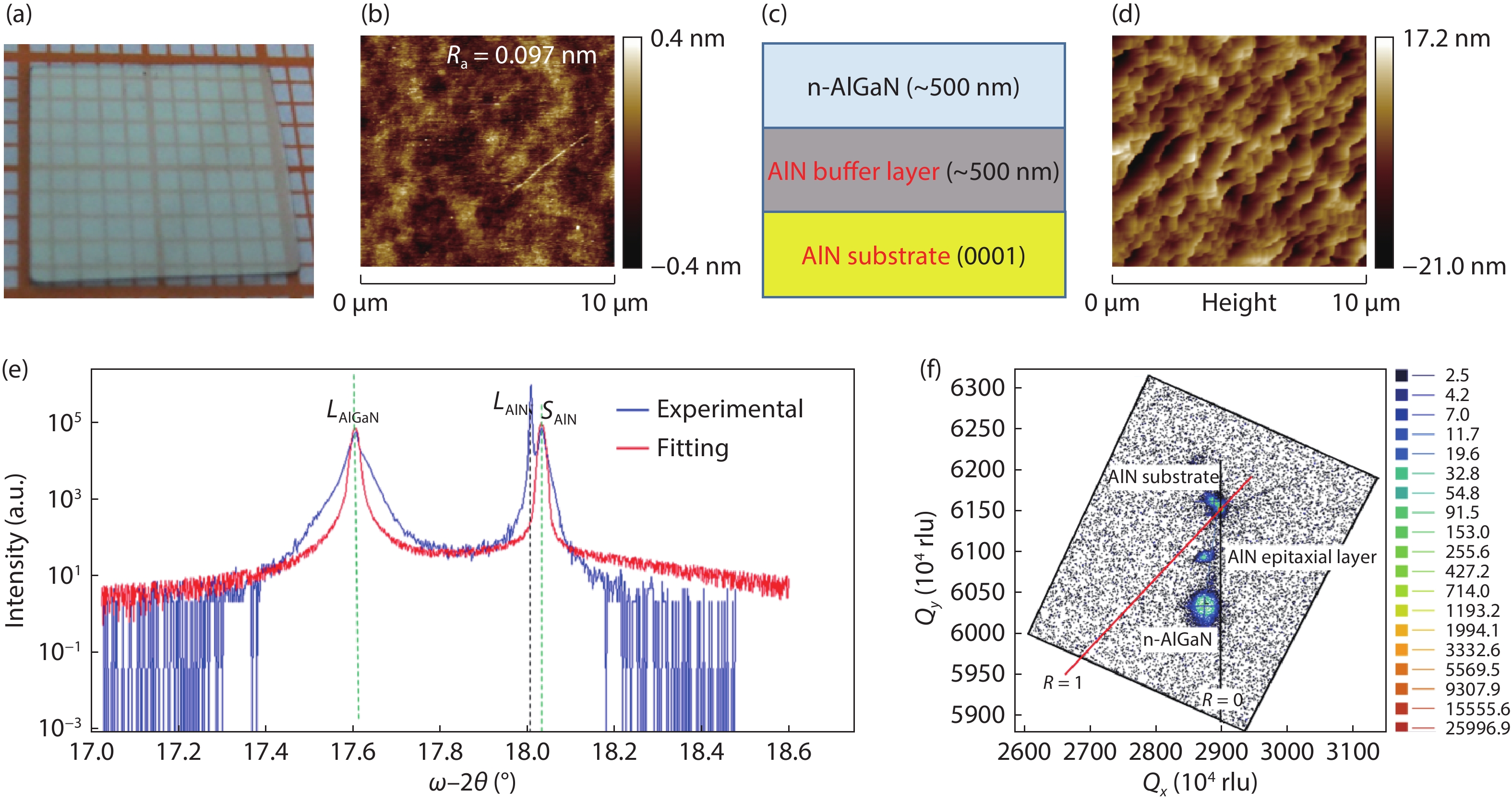
AlN single crystal grown by physical vapor transport (PVT) using homogeneous seed is considered as the most promising approach to obtain high-quality AlN boule. In this work, the morphology of AlN single crystals grown under different modes (3D islands and single spiral center) were investigated. It is proved that, within an optimized thermal distribution chamber system, the surface temperature of AlN seed plays an important role in crystal growth, revealing a direct relationship between growth mode and growth condition. Notably, a high-quality AlN crystal, with (002) and (102) reflection peaks of 65 and 36 arcsec at full width at half maximum (FWHM), was obtained grown under a single spiral center mode. And on which, a high-quality AlxGa1–xN epitaxial layer with high Al content (x = 0.54) was also obtained. The FWHMs of (002) and (102) reflection of AlxGa1–xN were 202 and 496 arcsec, respectively, which shows superiority over their counterpart grown on SiC or a sapphire substrate.


J. Semicond.
2021, 42(5): 052301 doi: 10.1088/1674-4926/42/5/052301
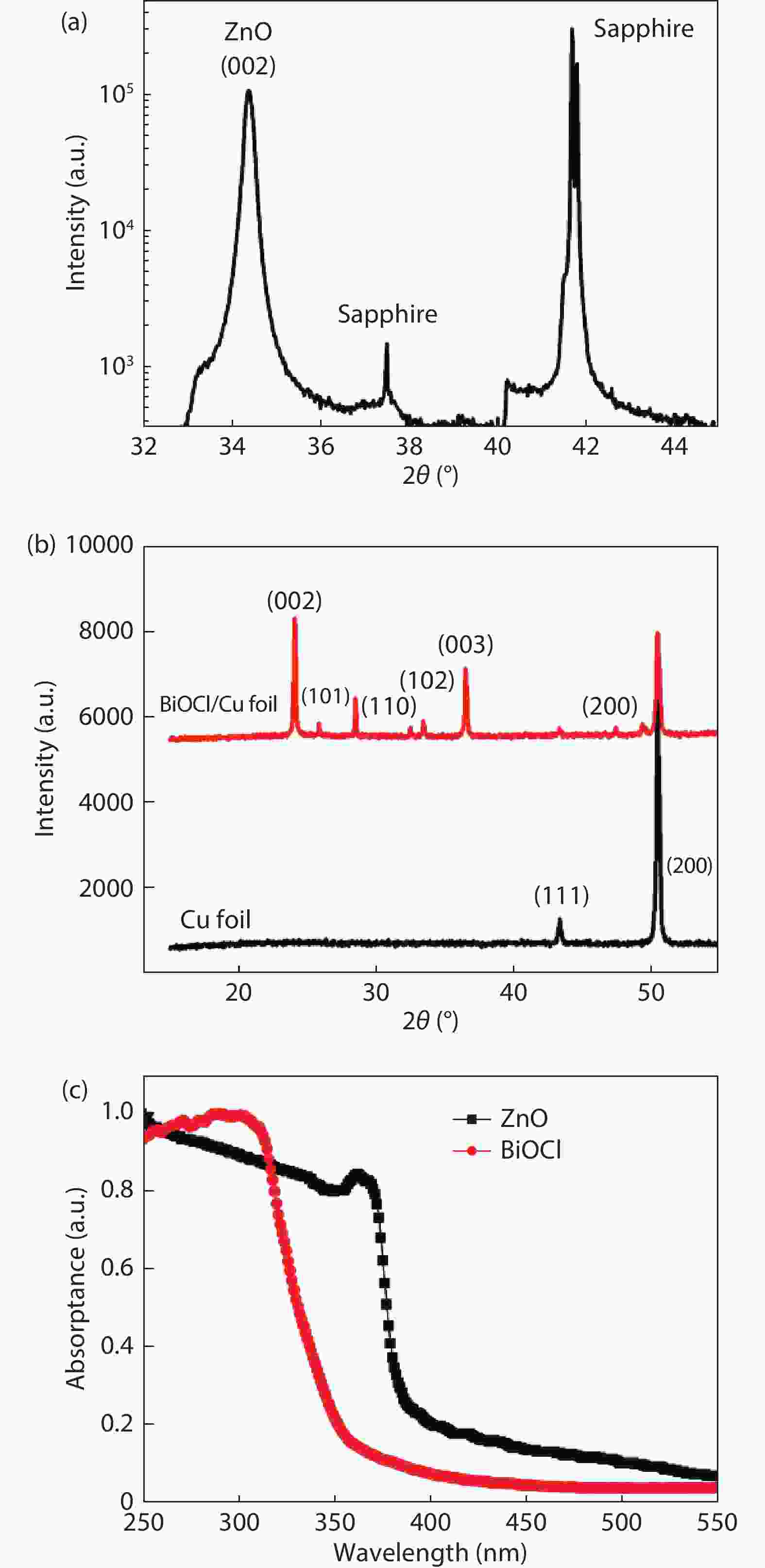
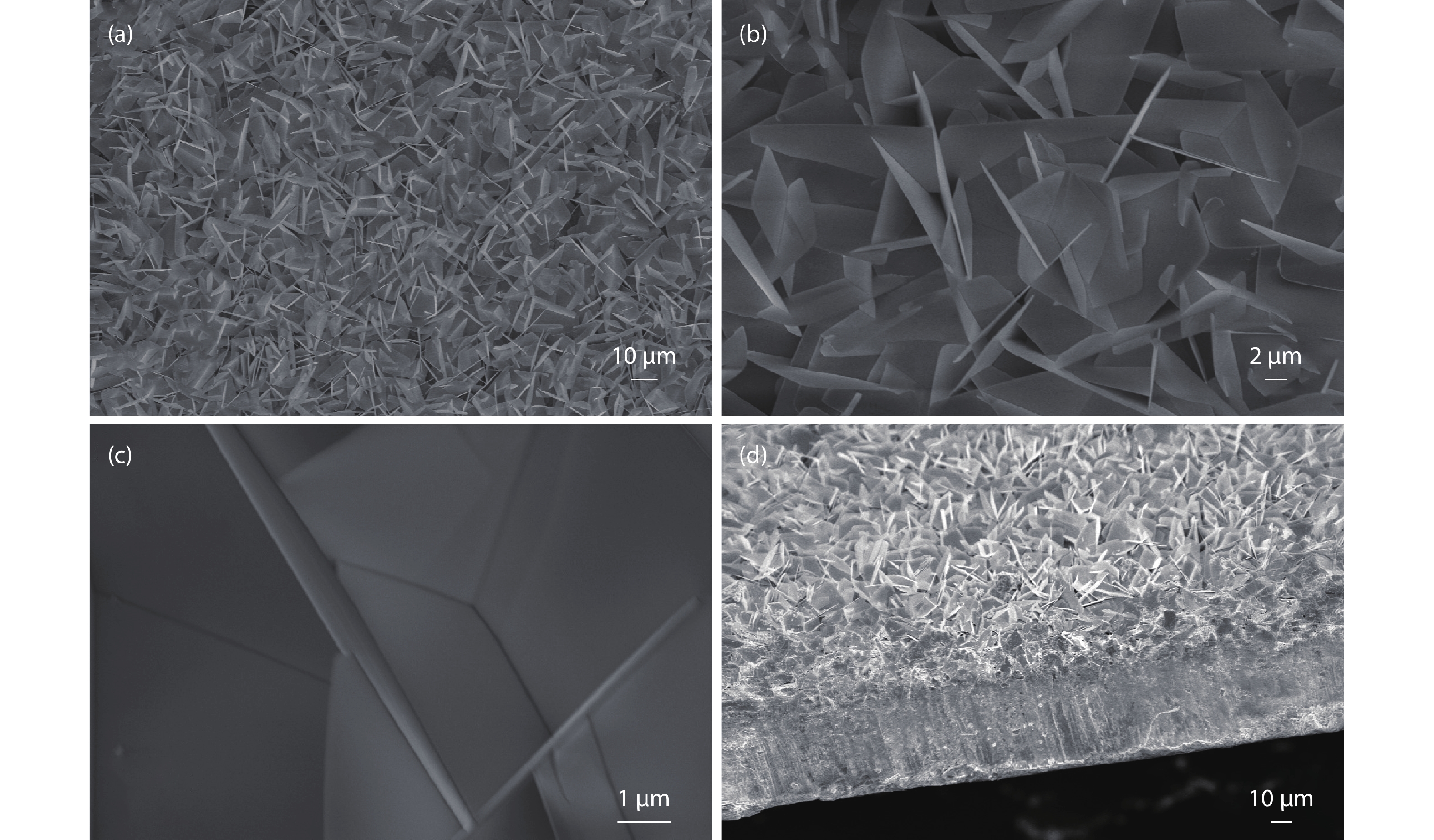
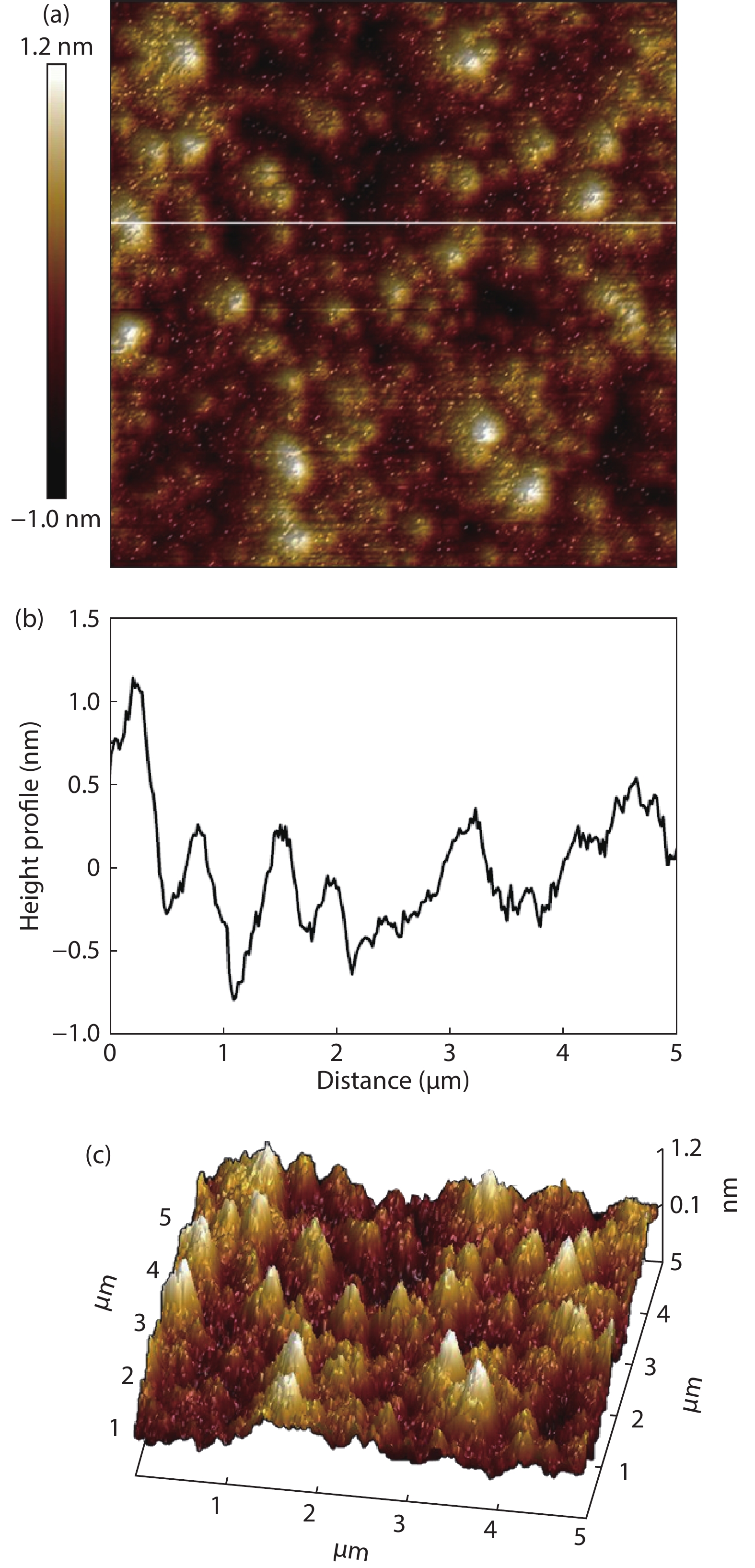
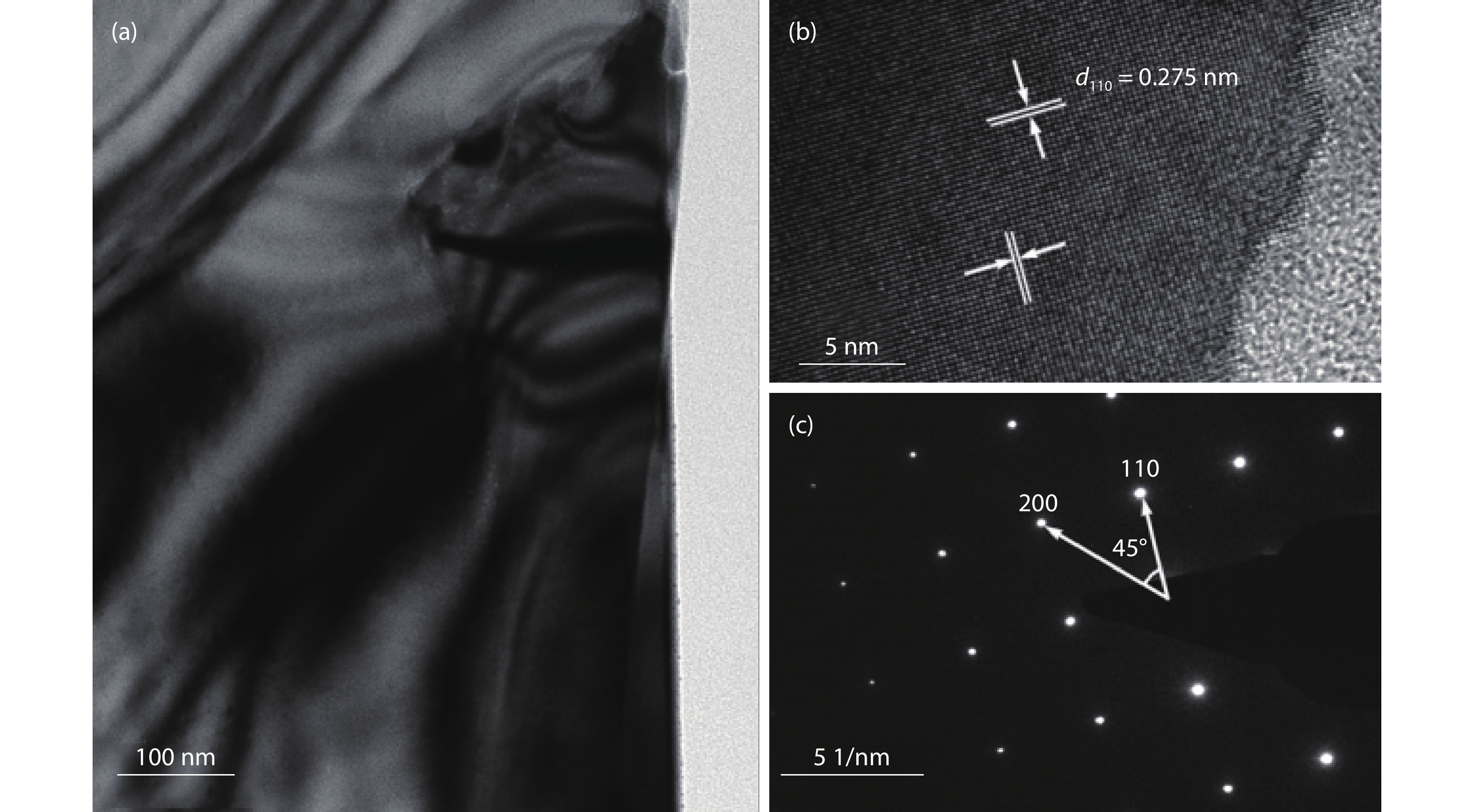
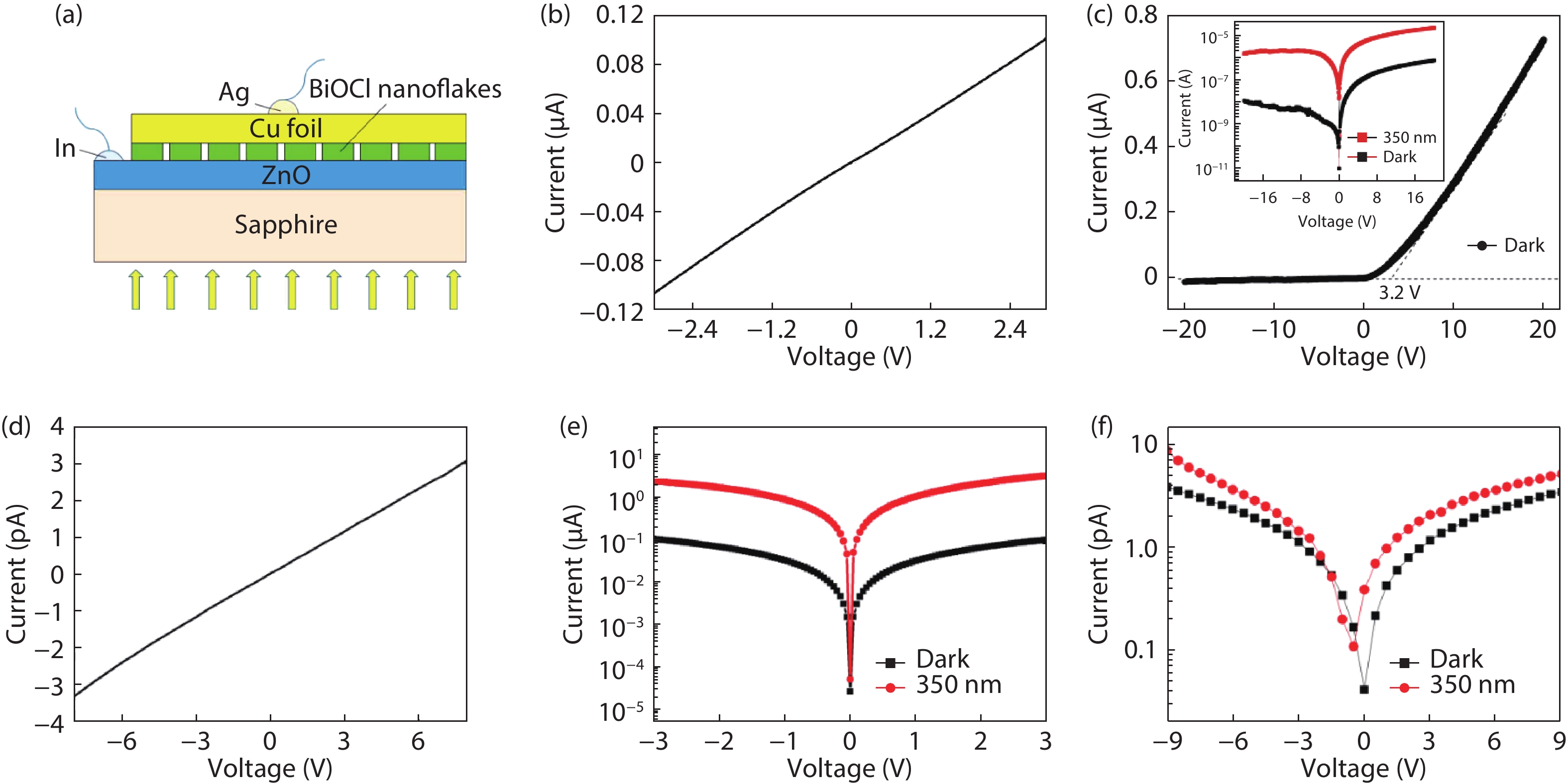
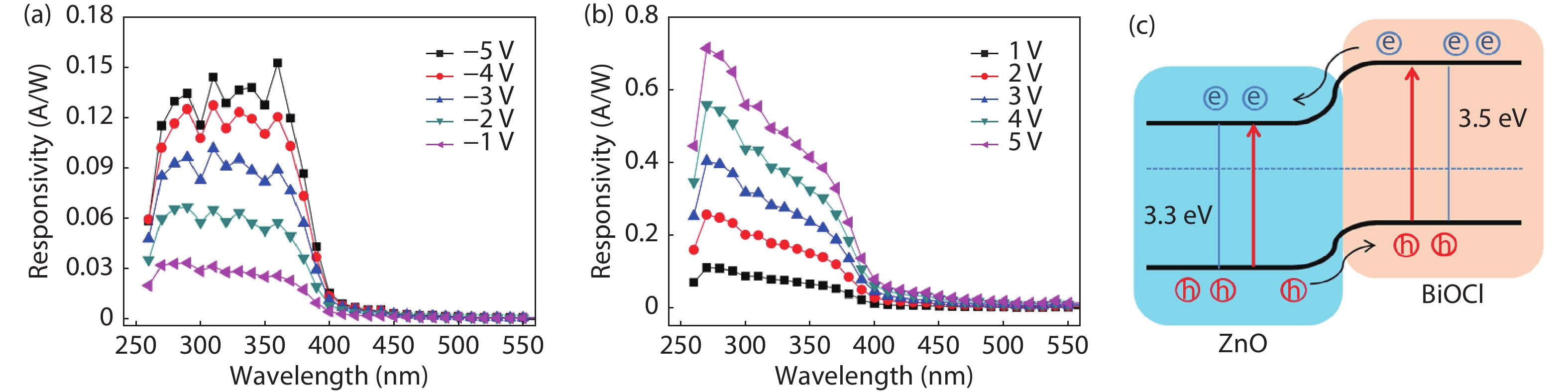
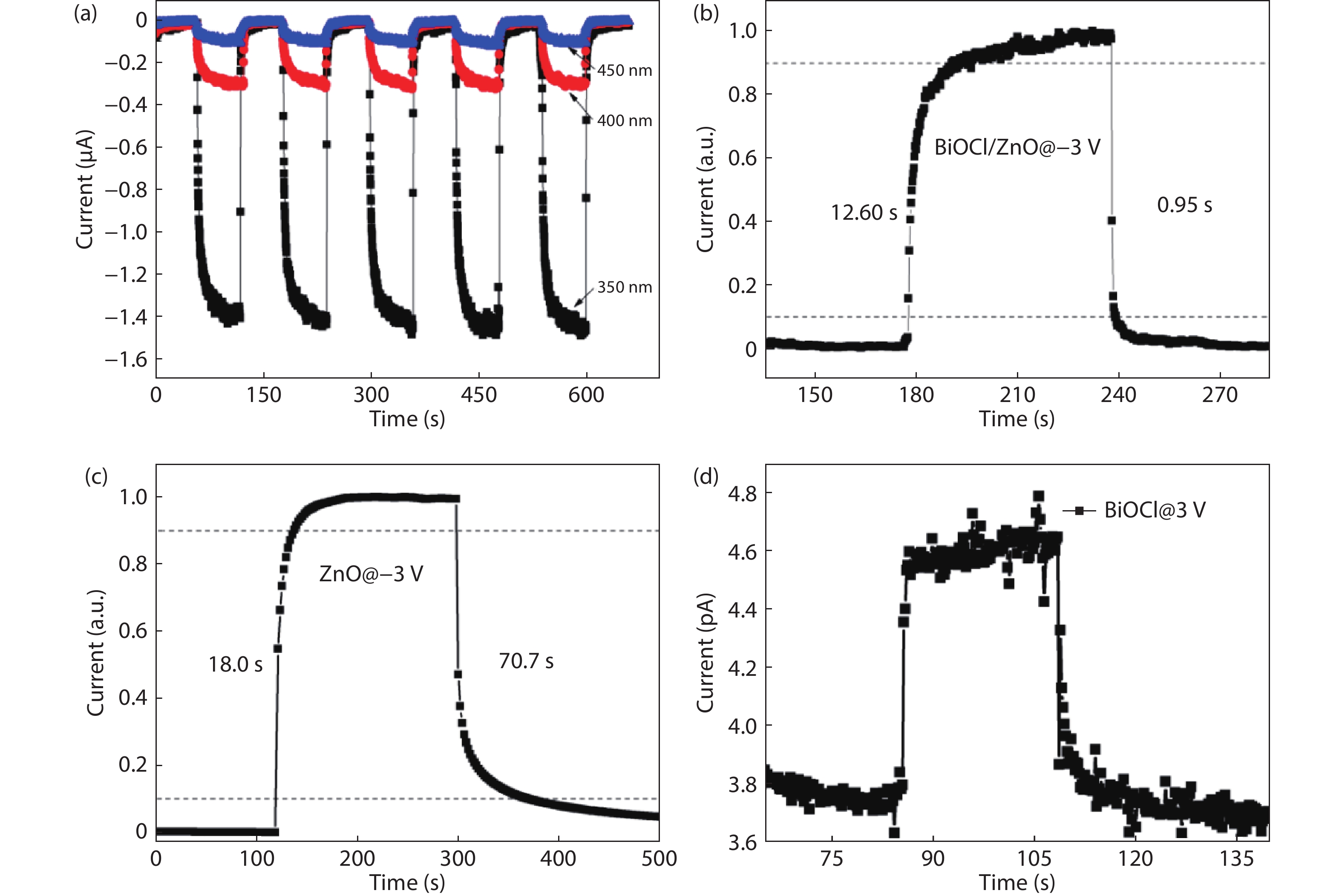
Herein, high-quality n-ZnO film layer on c-sapphire and well-crystallized tetragonal p-BiOCl nanoflakes on Cu foil are prepared, respectively. According to the absorption spectra, the bandgaps of n-ZnO and p-BiOCl are confirmed as ~3.3 and ~3.5 eV, respectively. Subsequently, a p-BiOCl/n-ZnO heterostructural photodetector is constructed after a facile mechanical bonding and post annealing process. At –5 V bias, the photocurrent of the device under 350 nm irradiation is ~800 times higher than that in dark, which indicates its strong UV light response characteristic. However, the on/off ratio of In–ZnO–In photodetector is ~20 and the Cu–BiOCl–Cu photodetector depicts very weak UV light response. The heterostructure device also shows a short decay time of 0.95 s, which is much shorter than those of the devices fabricated from pure ZnO thin film and BiOCl nanoflakes. The p-BiOCl/n-ZnO heterojunction photodetector provides a promising pathway to multifunctional UV photodetectors with fast response, high signal-to-noise ratio, and high selectivity.

J. Semicond.
2021, 42(5): 052401 doi: 10.1088/1674-4926/42/5/052401
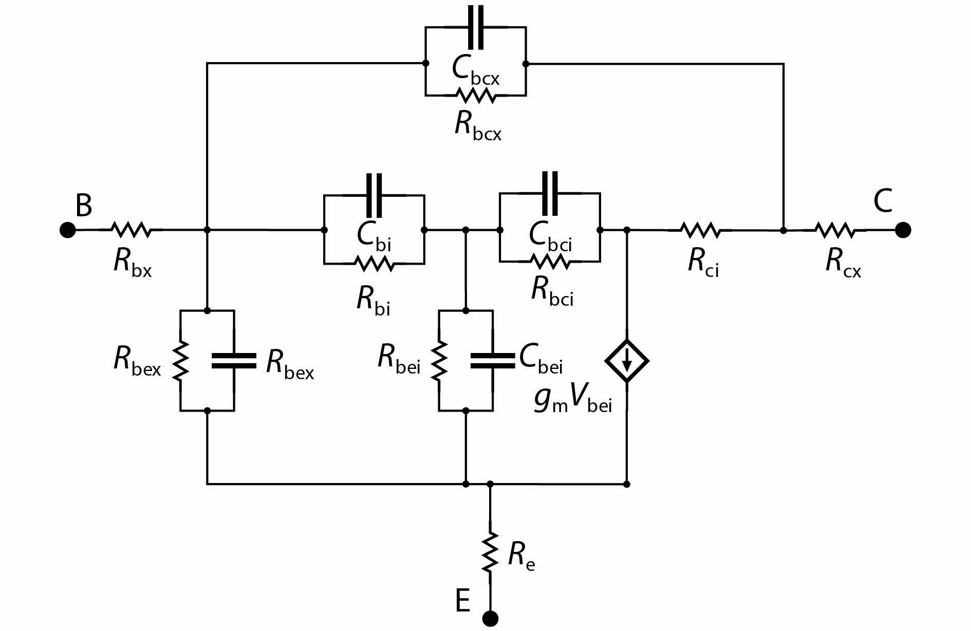
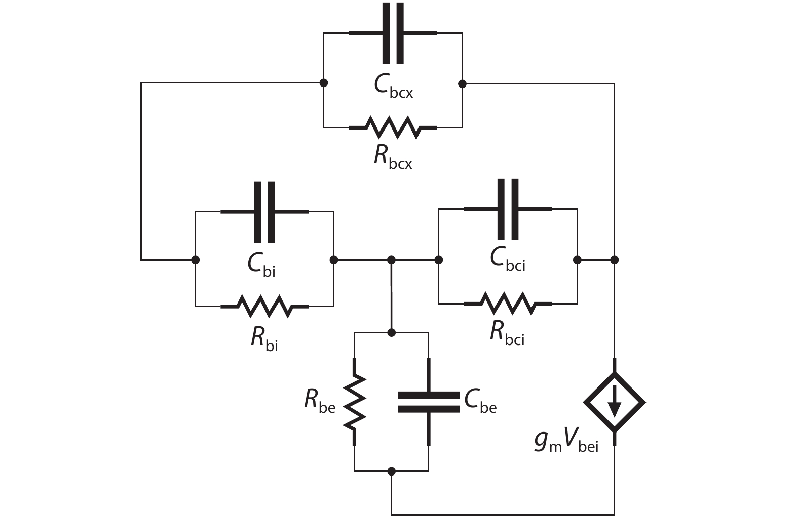
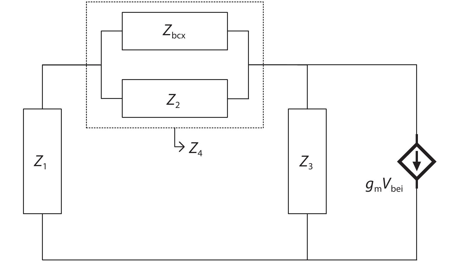
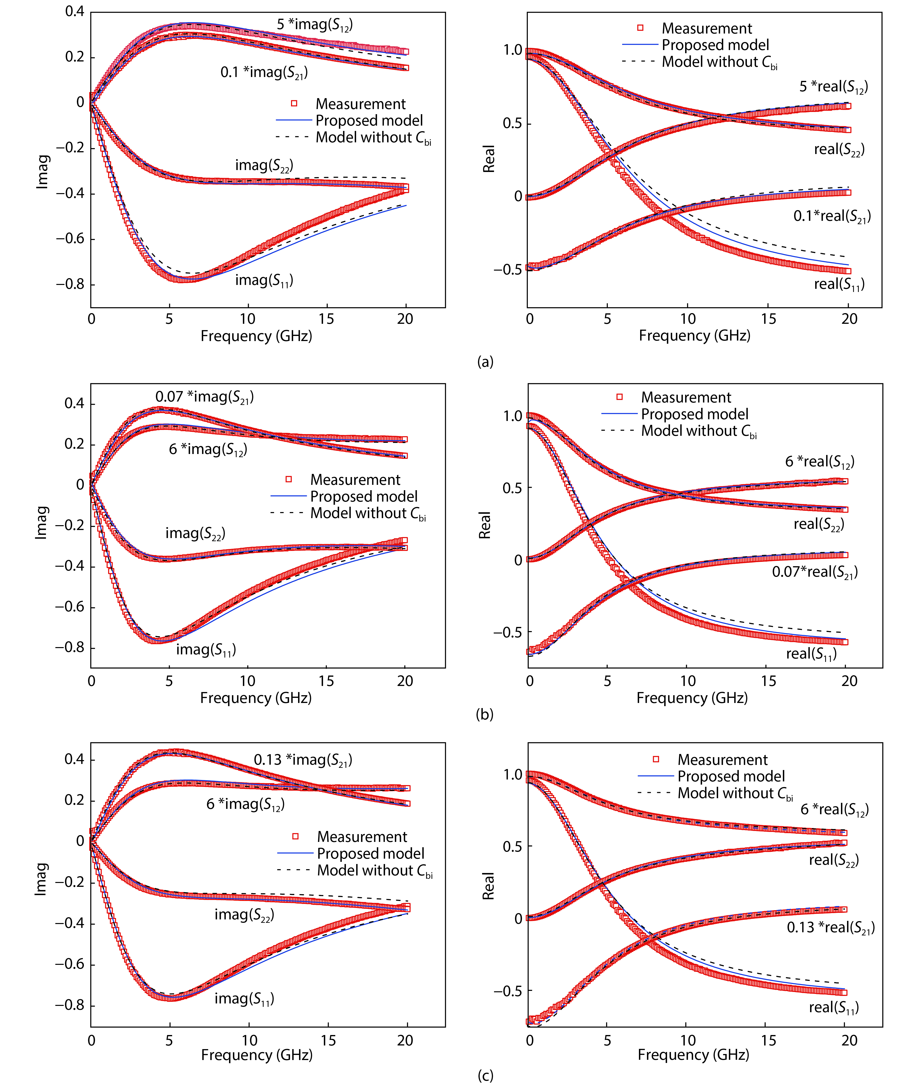
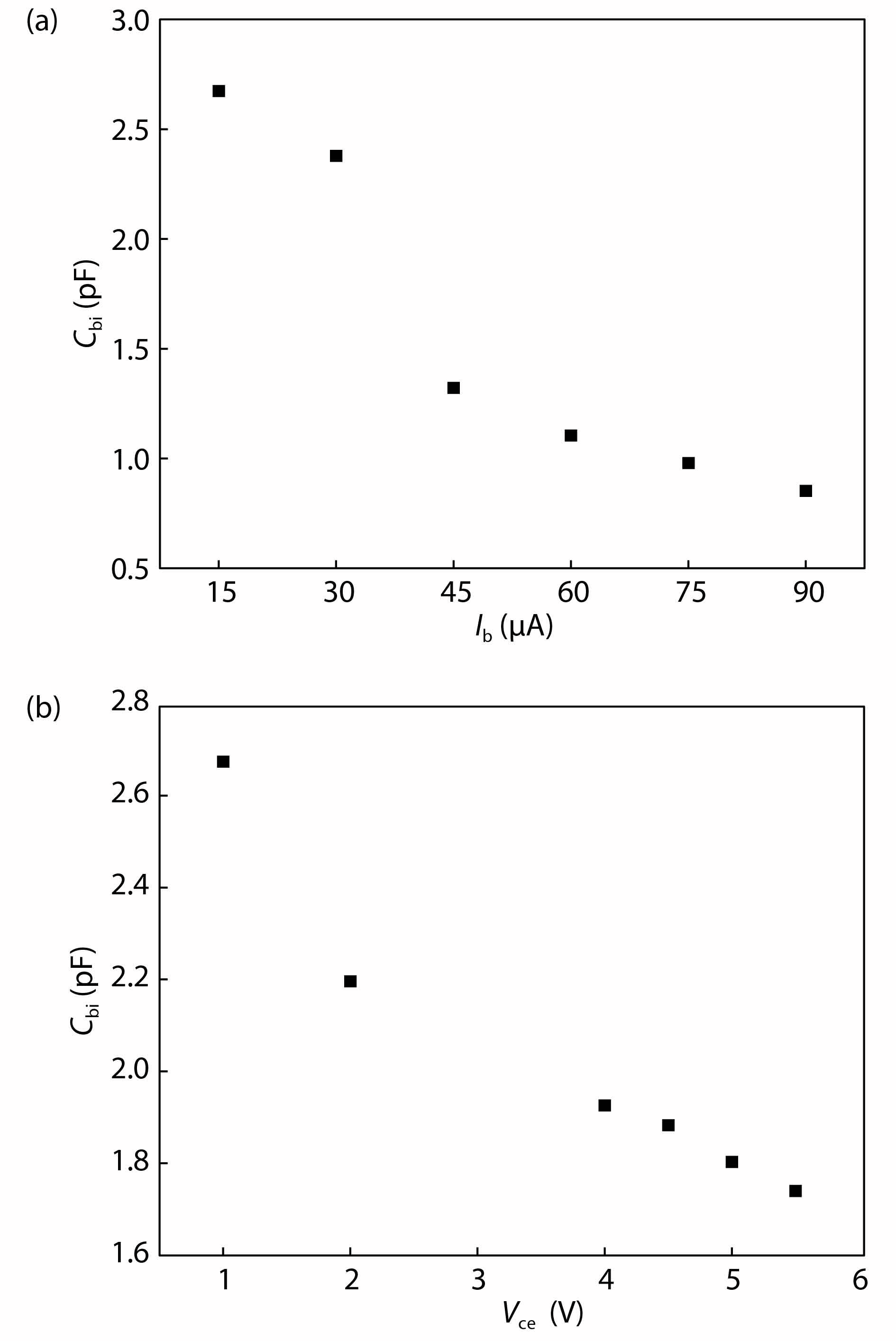
An improved small-signal equivalent circuit of HBT concerning the AC current crowding effect is proposed in this paper. AC current crowding effect is modeled as a parallel RC circuit composed of Cbi and Rbi, with distributed base-collector junction capacitance also taken into account. The intrinsic portion is taken as a whole and extracted directly from the measured S-parameters in the whole frequency range of operation without any special test structures. An HBT device with a 2 × 20 μm2 emitter-area under three different biases were used to demonstrate the extraction and verify the accuracy of the equivalent circuit.

J. Semicond.
2021, 42(5): 052402 doi: 10.1088/1674-4926/42/5/052402
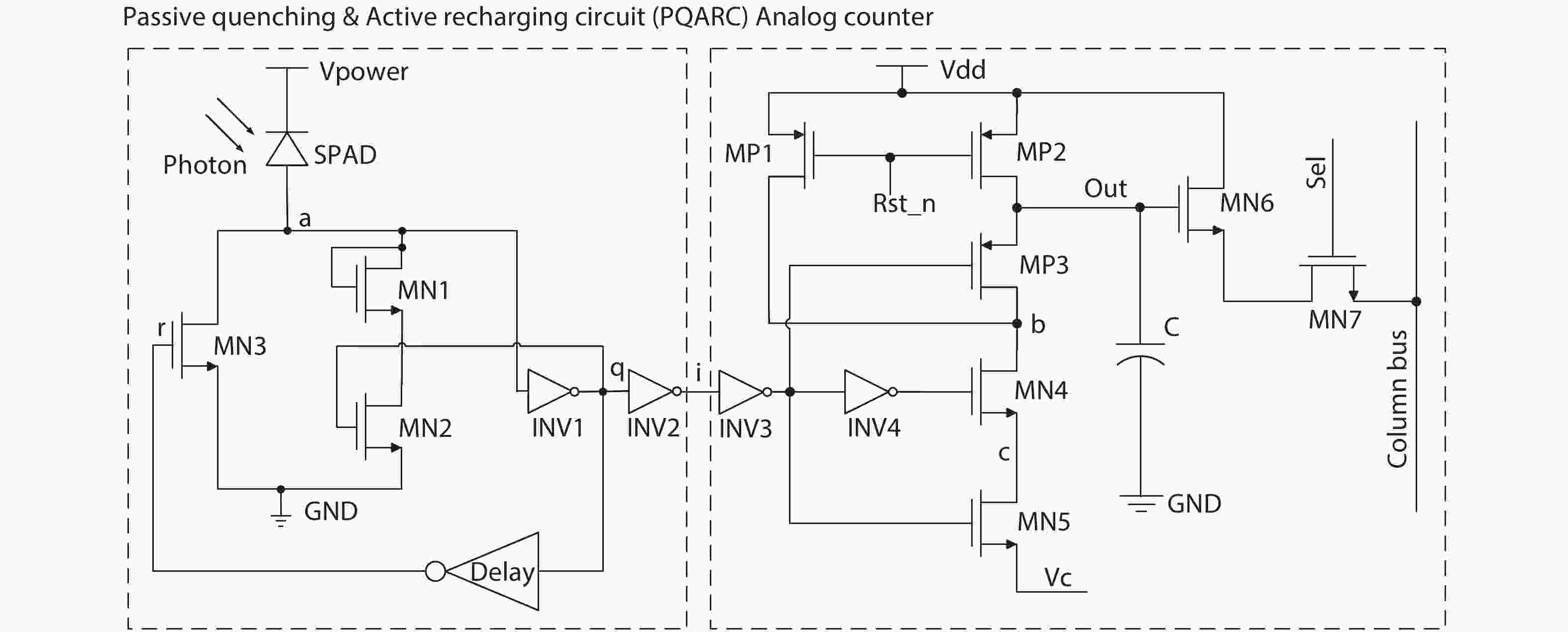
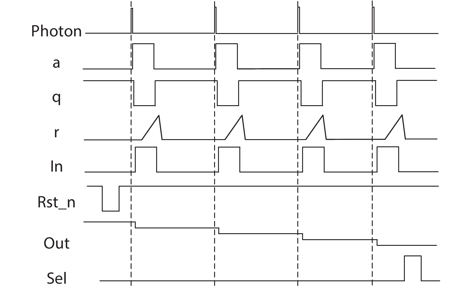
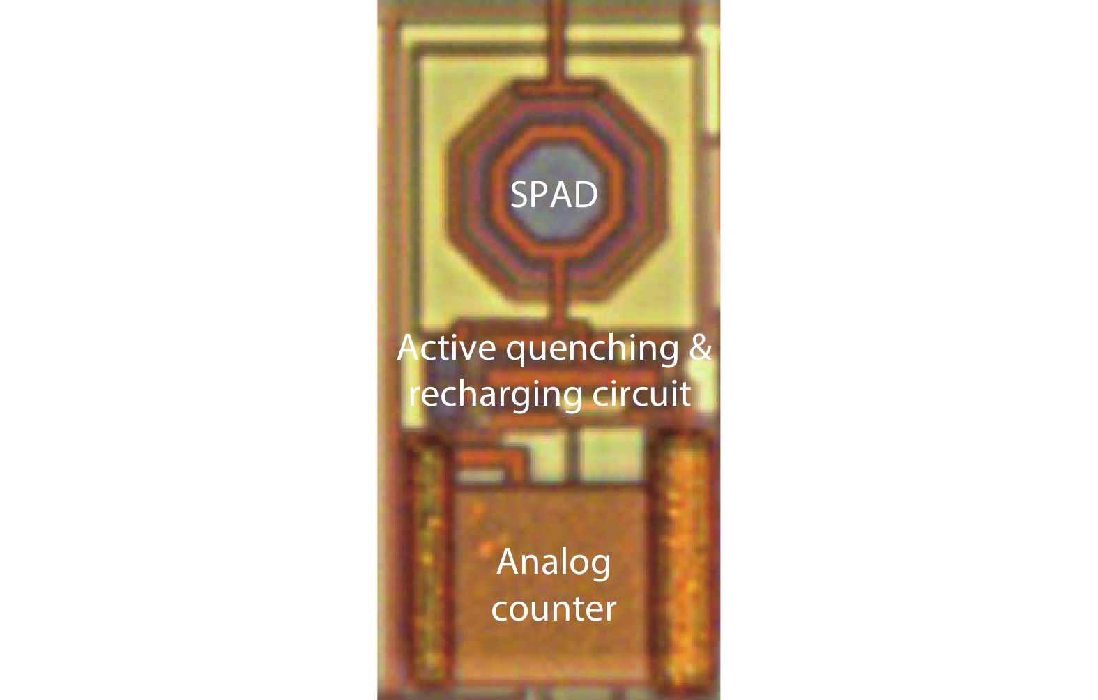
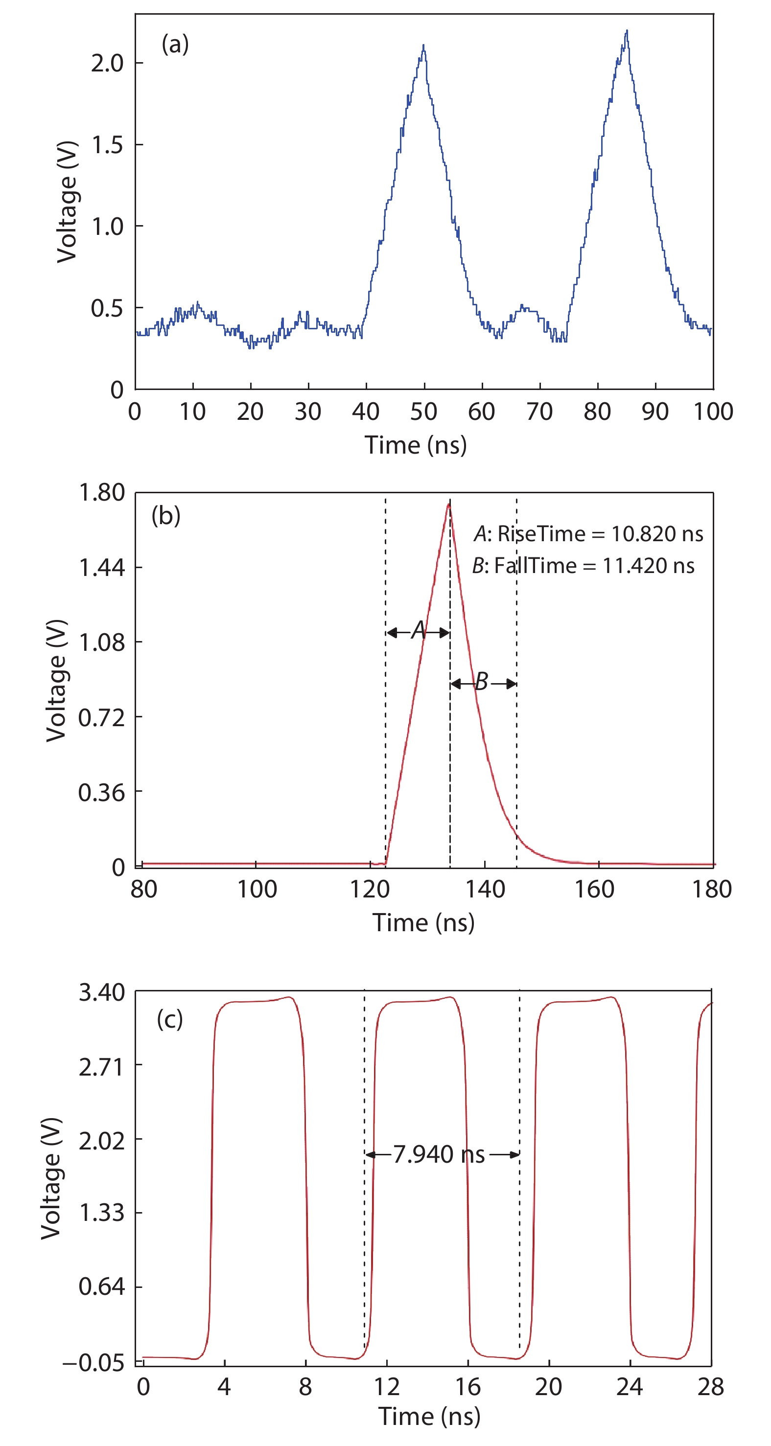
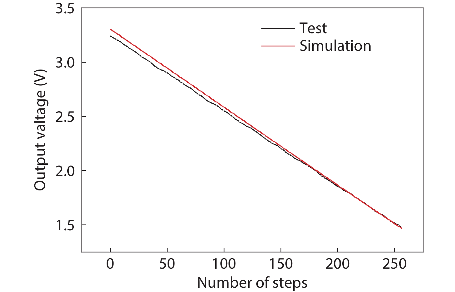
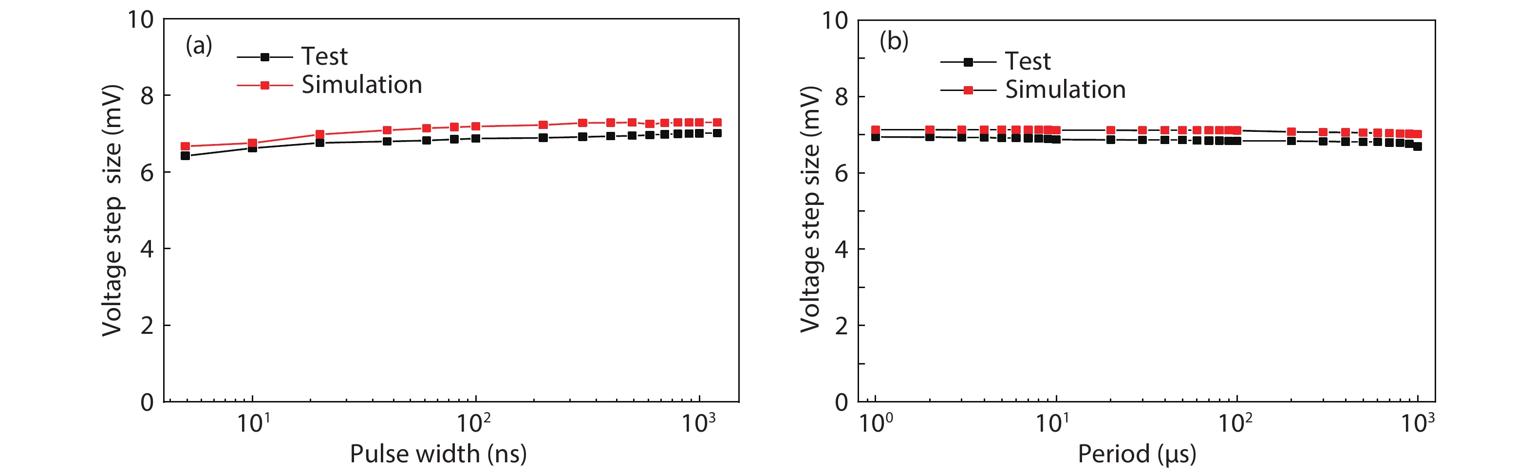
A compact pixel for single-photon detection in the analog domain is presented. The pixel integrates a single-photon avalanche diode (SPAD), a passive quenching & active recharging circuit (PQARC), and an analog counter for fast and accurate sensing and counting of photons. Fabricated in a standard 0.18 µm CMOS technology, the simulated and experimental results reveal that the dead time of the PQARC is about 8 ns and the maximum photon-counting rate can reach 125 Mcps (counting per second). The analog counter can achieve an 8-bit counting range with a voltage step of 6.9 mV. The differential nonlinearity (DNL) and integral nonlinearity (INL) of the analog counter are within the ± 0.6 and ± 1.2 LSB, respectively, indicating high linearity of photon counting. Due to its simple circuit structure and compact layout configuration, the total area occupation of the presented pixel is about 1500 μm2, leading to a high fill factor of 9.2%. The presented in-pixel front-end circuit is very suitable for the high-density array integration of SPAD sensors.


J. Semicond.
2021, 42(5): 052701 doi: 10.1088/1674-4926/42/5/052701
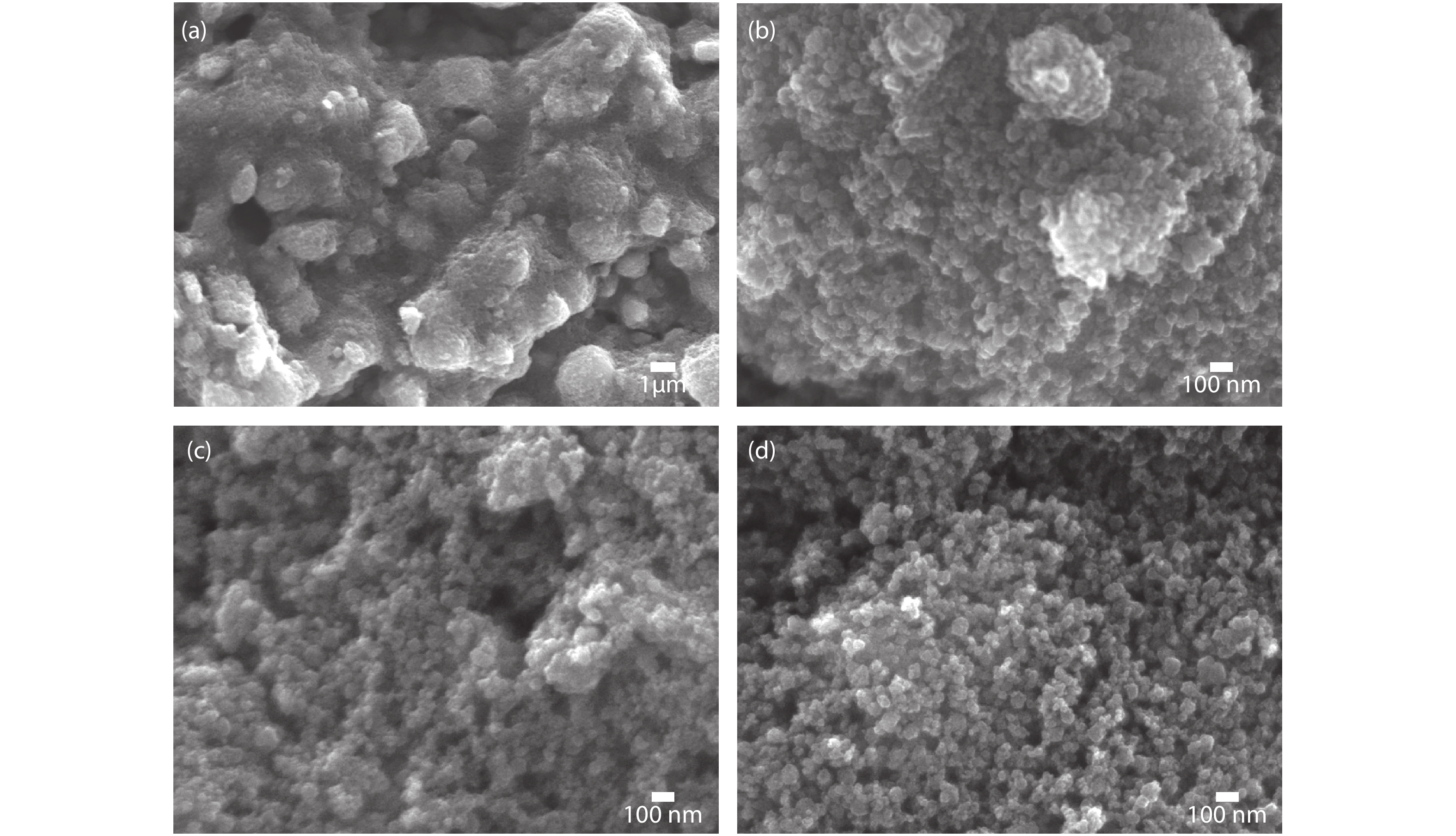
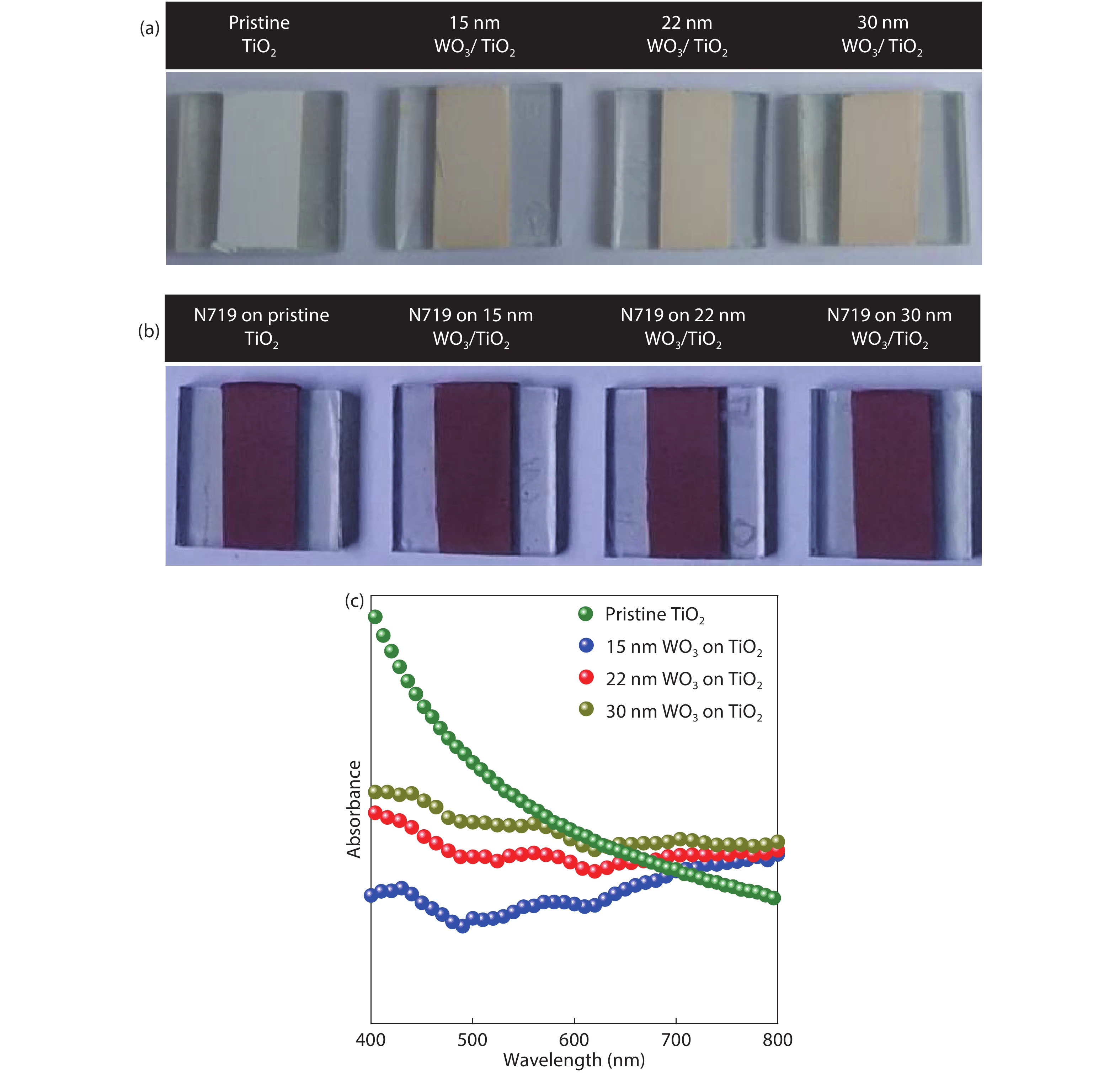
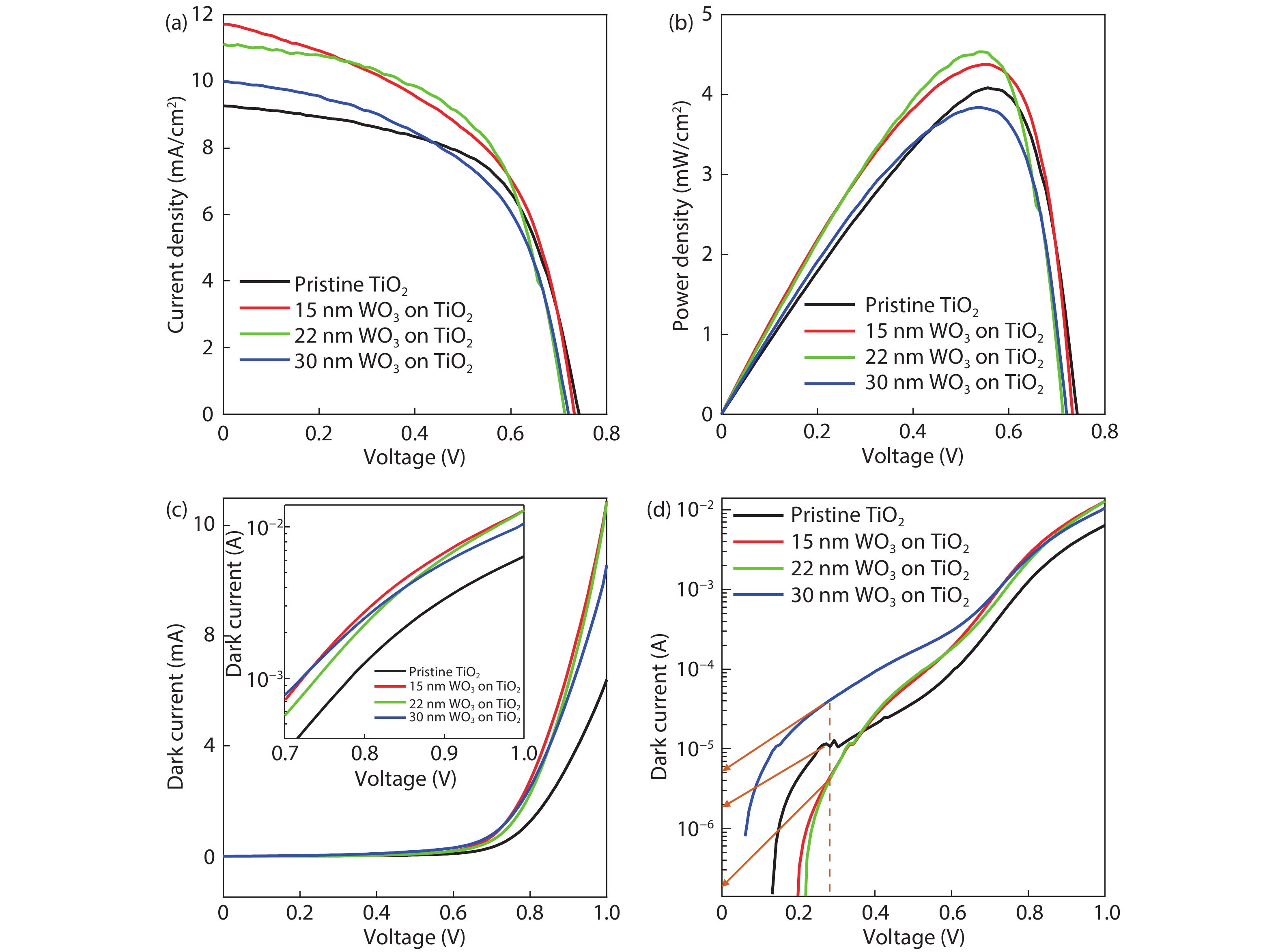
Major loss factors for photo-generated electrons due to the presence of surface defects in titanium dioxide (TiO2) were controlled by RF-sputtered tungsten trioxide (WO3) passivation. X-ray photoelectron spectroscopy assured the coating of WO3 on the TiO2 nanoparticle layer by showing Ti 2p, W 4f and O 1s characteristic peaks and were further confirmed by X-ray diffraction studies. The coating of WO3 on the TiO2 nanoparticle layer did not affect dye adsorption significantly. Dye sensitized solar cells (DSSCs) fabricated using WO3-coated TiO2 showed an enhancement of ~10% compared to DSSCs fabricated using pristine TiO2-based photo-electrodes. It is attributed to the WO3 passivation on TiO2 that creates an energy barrier which favored photo-electron injection by tunneling but blocked reverse electron recombination pathways towards holes available in highest occupied molecular orbital of the dye molecules. It was further evidenced that there is an optimum thickness (duration of coating) of WO3 to improve the DSSC performance and longer duration of WO3 suppressed photo-electron injection from dye to TiO2 as inferred from the detrimental effect in short circuit current density values. RF-sputtering yields pinhole-free, highly uniform and conformal coating of WO3 onto any area of interest, which can be considered for an effective surface passivation for nanostructured photovoltaic devices.