Issue Browser
Volume 43, Issue 1,
Jan 2022


J. Semicond.
2022, 43(1): 011001 doi: 10.1088/1674-4926/43/1/011001

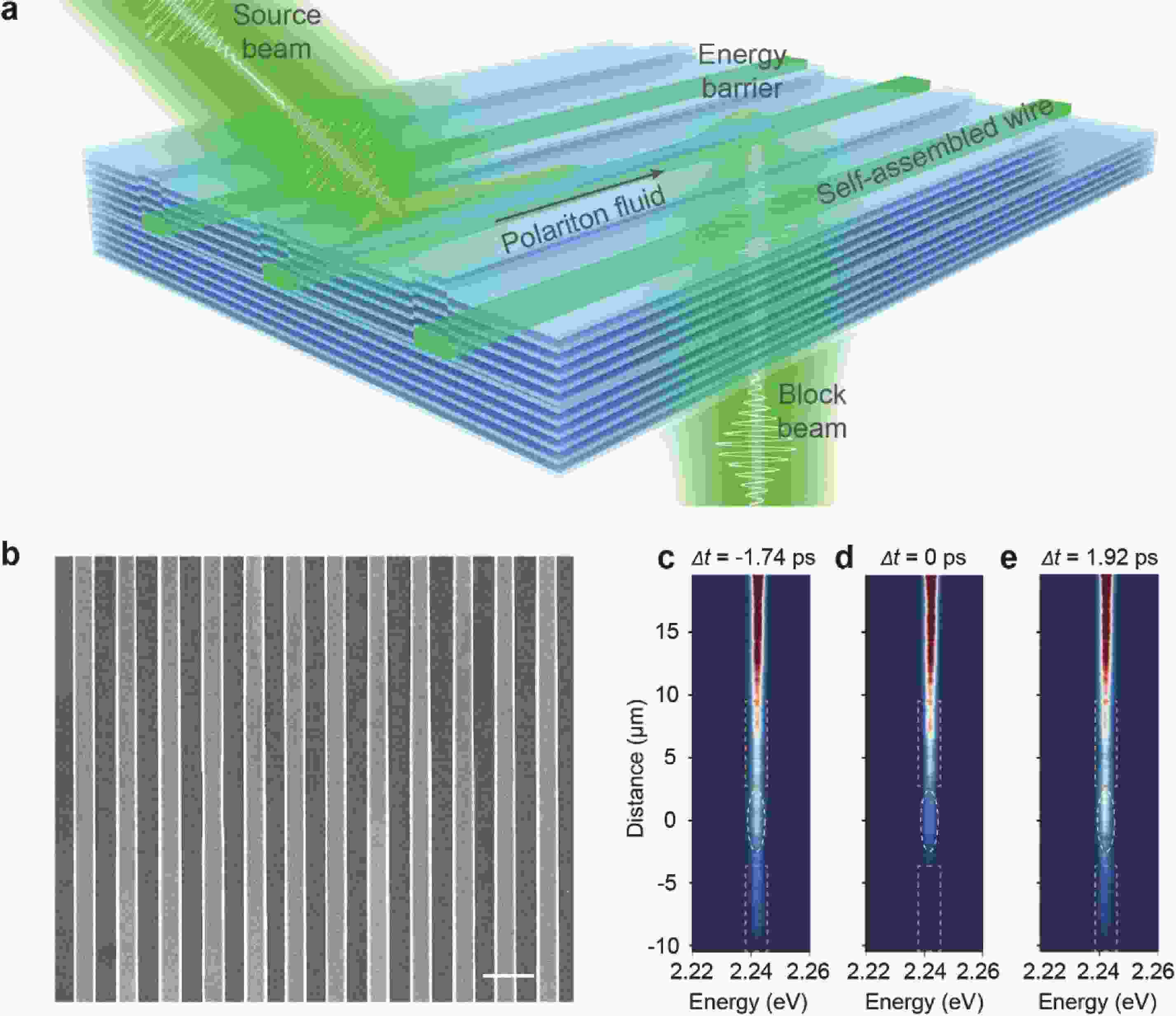
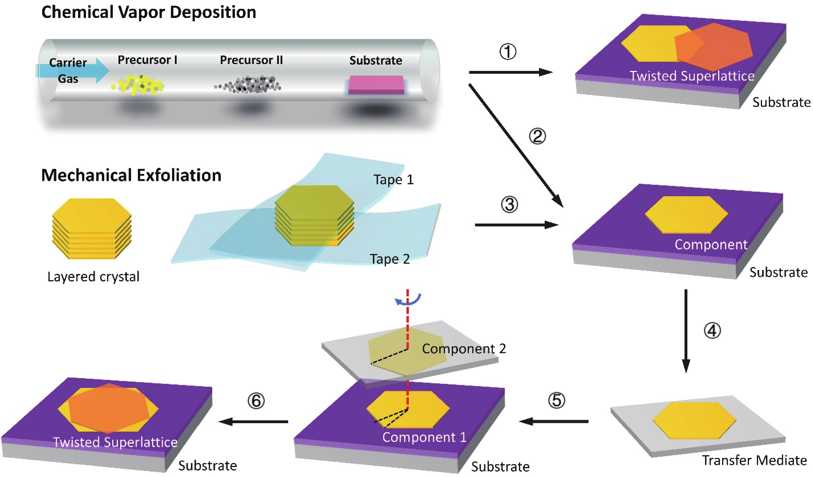
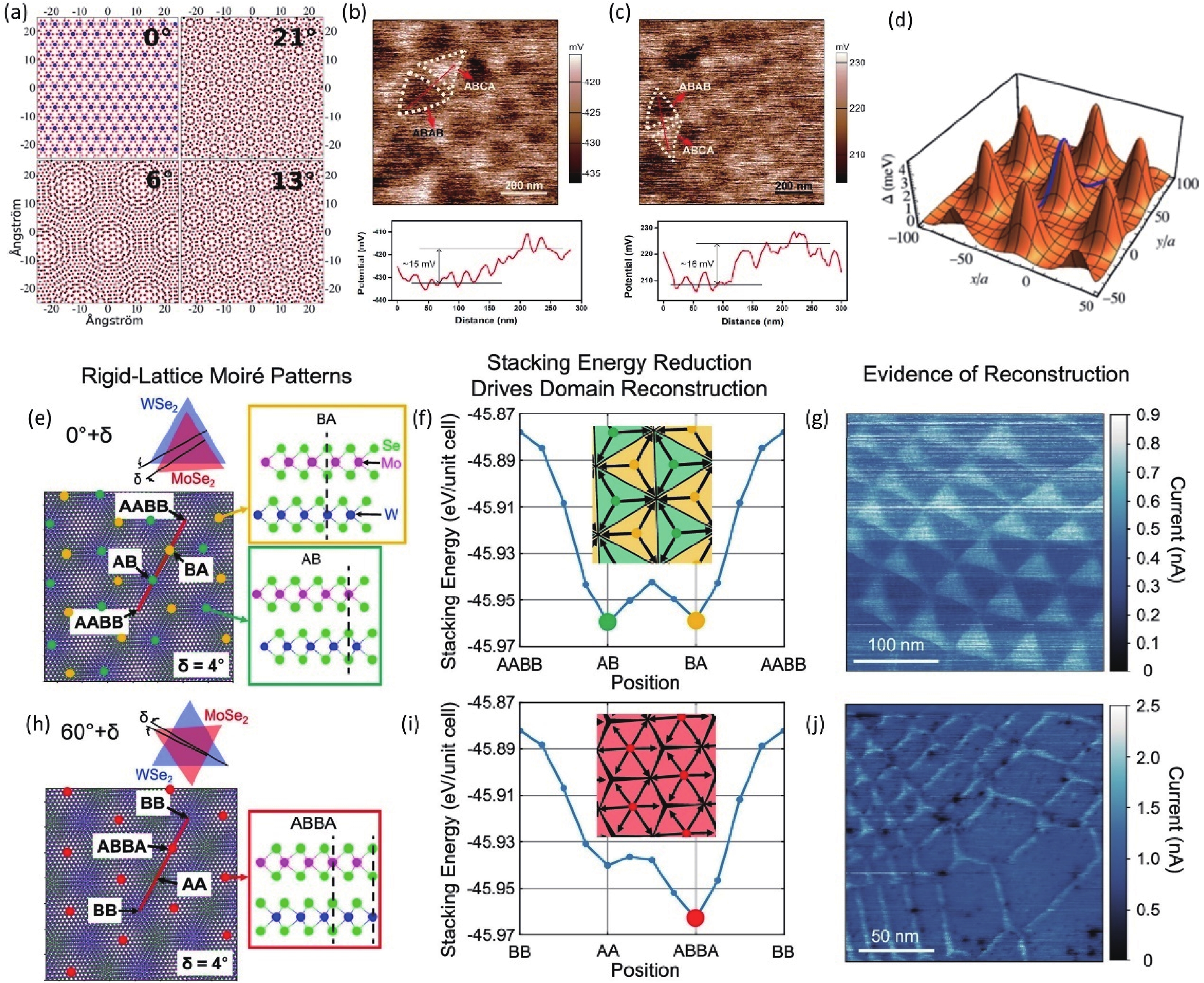
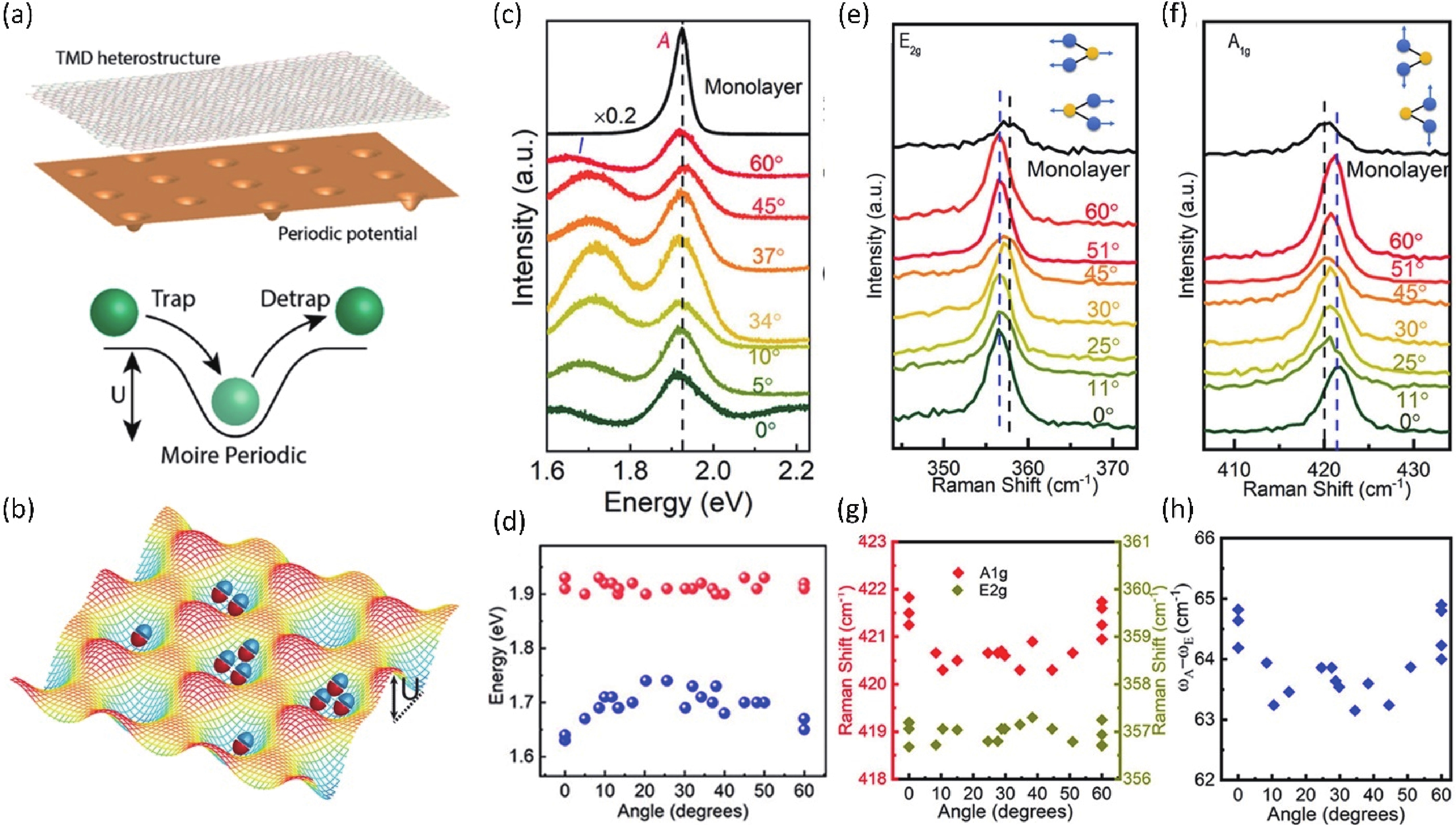
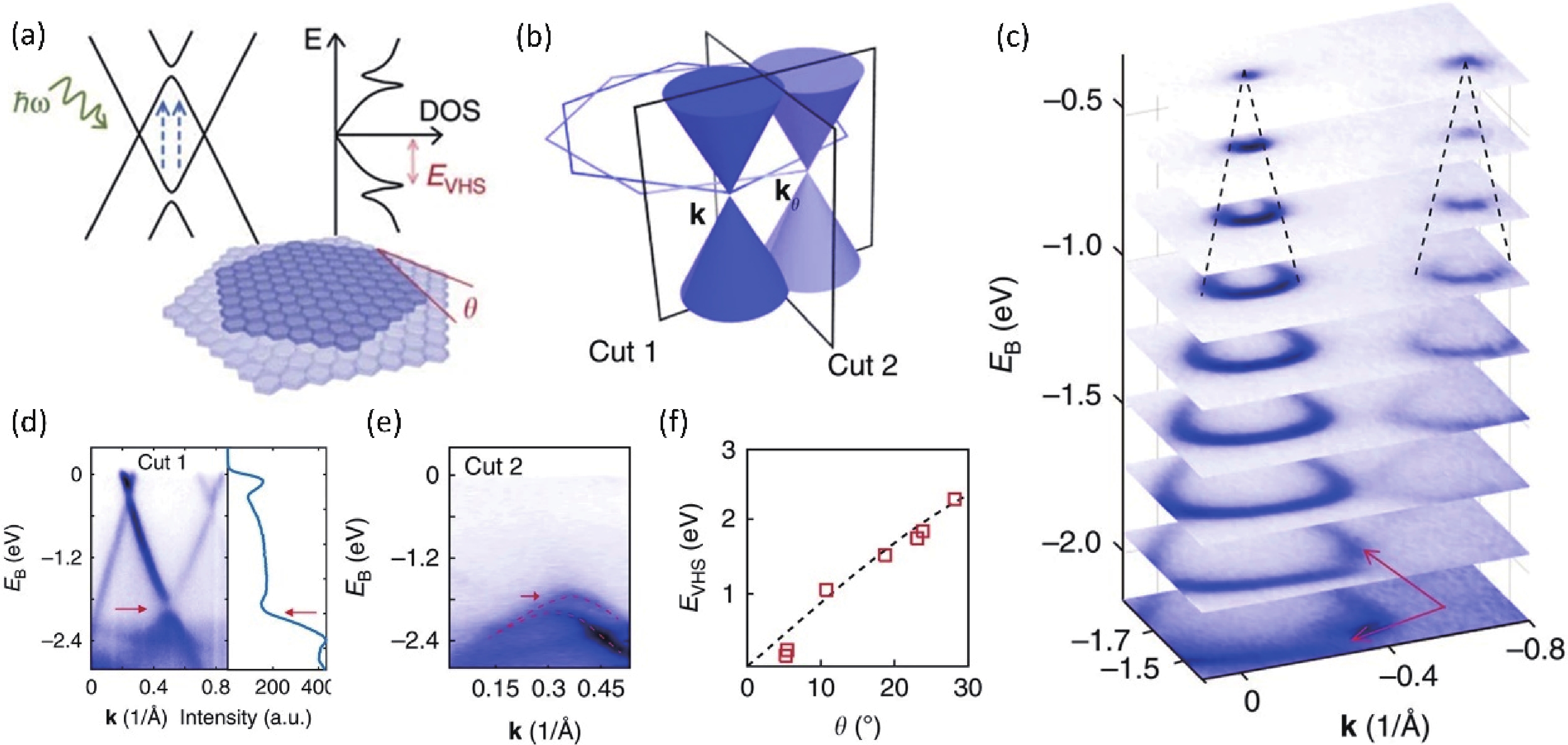
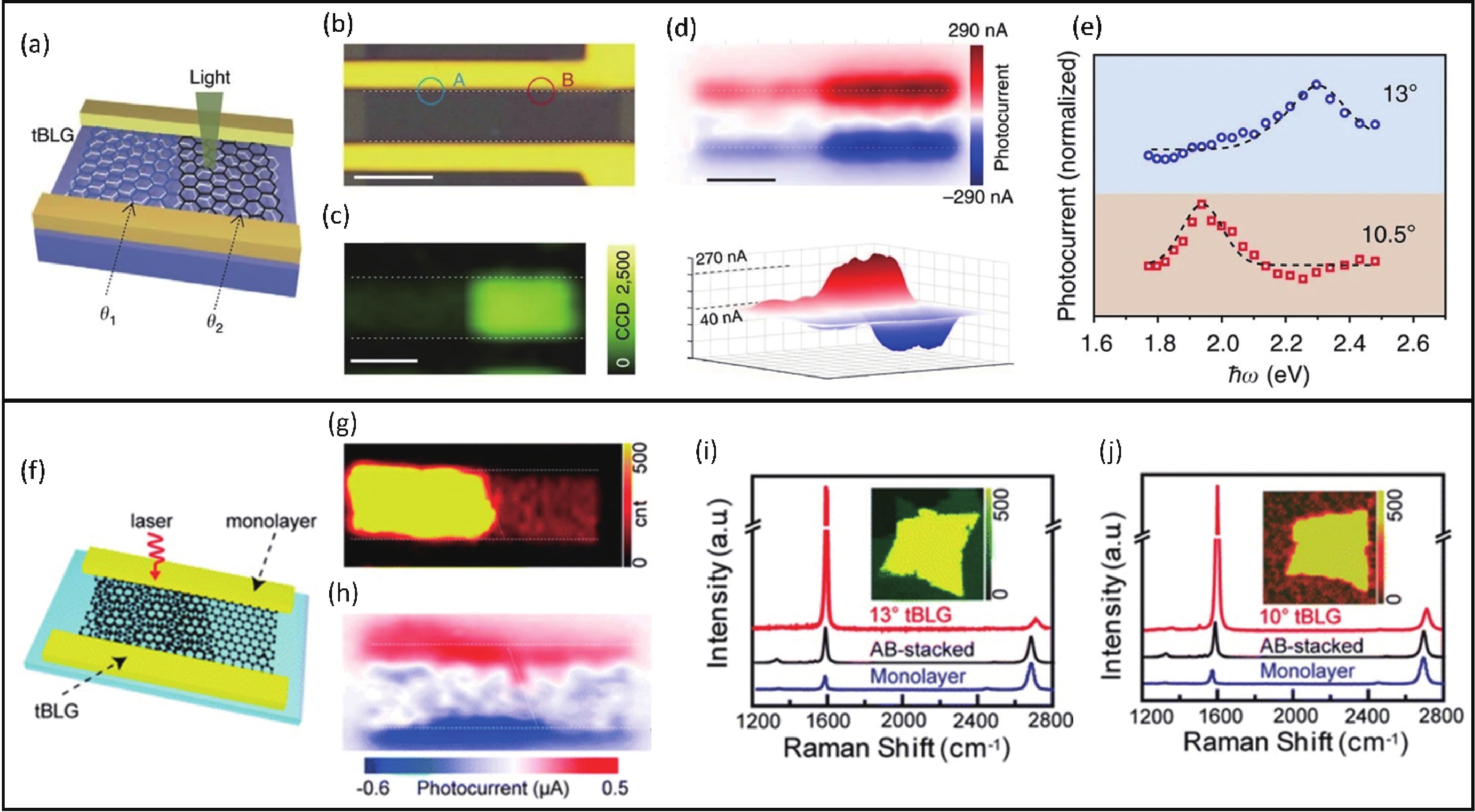
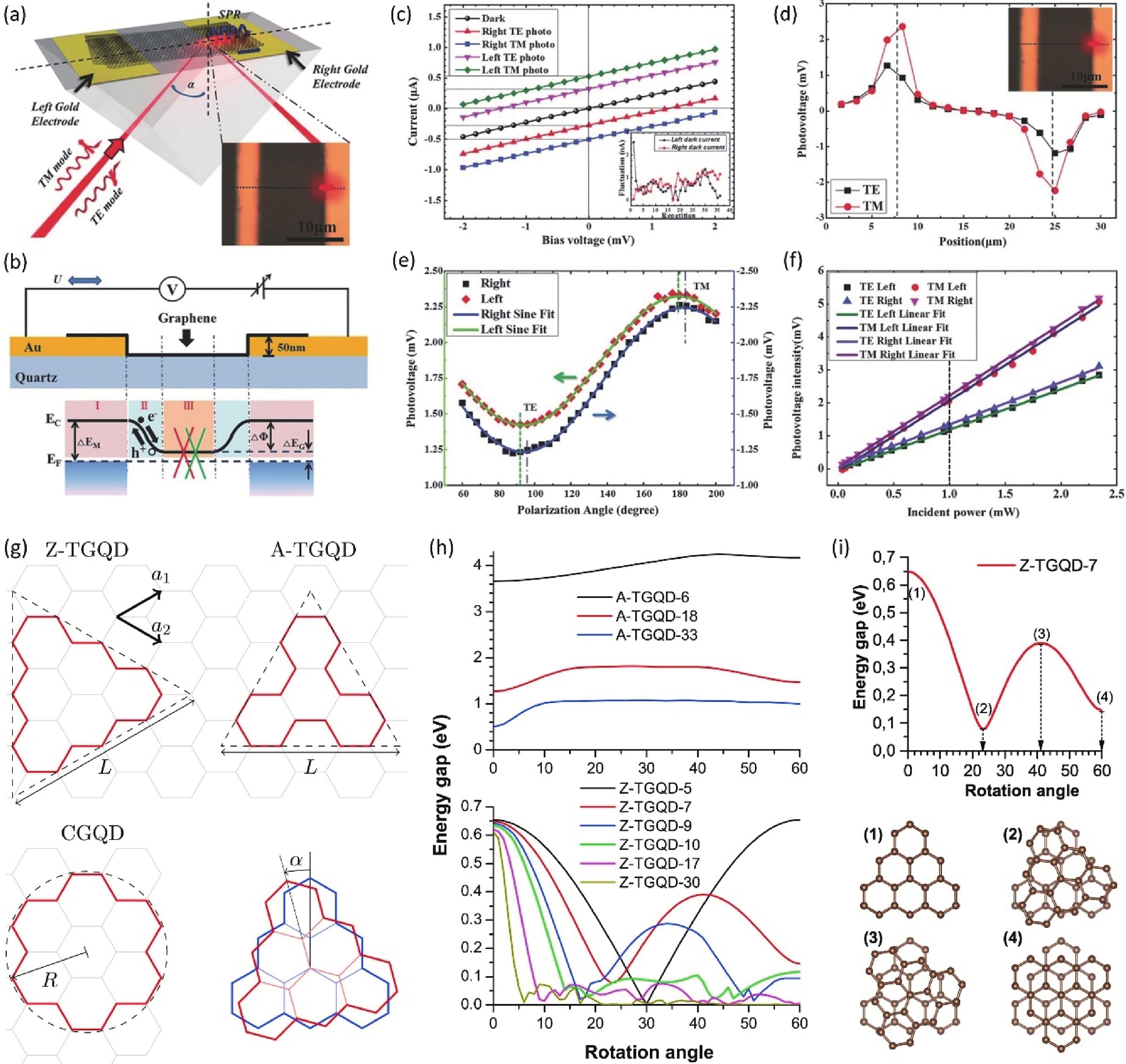
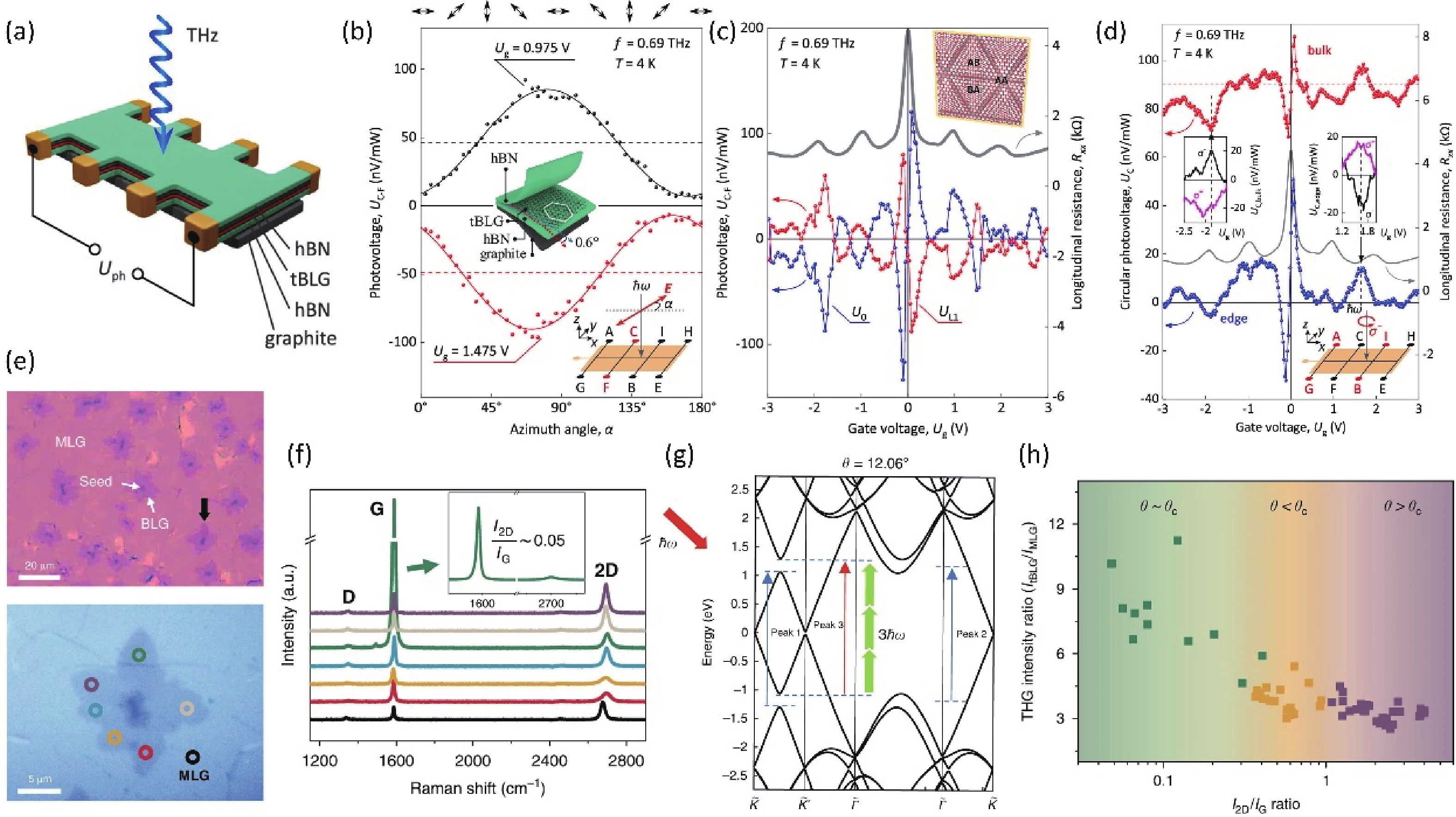
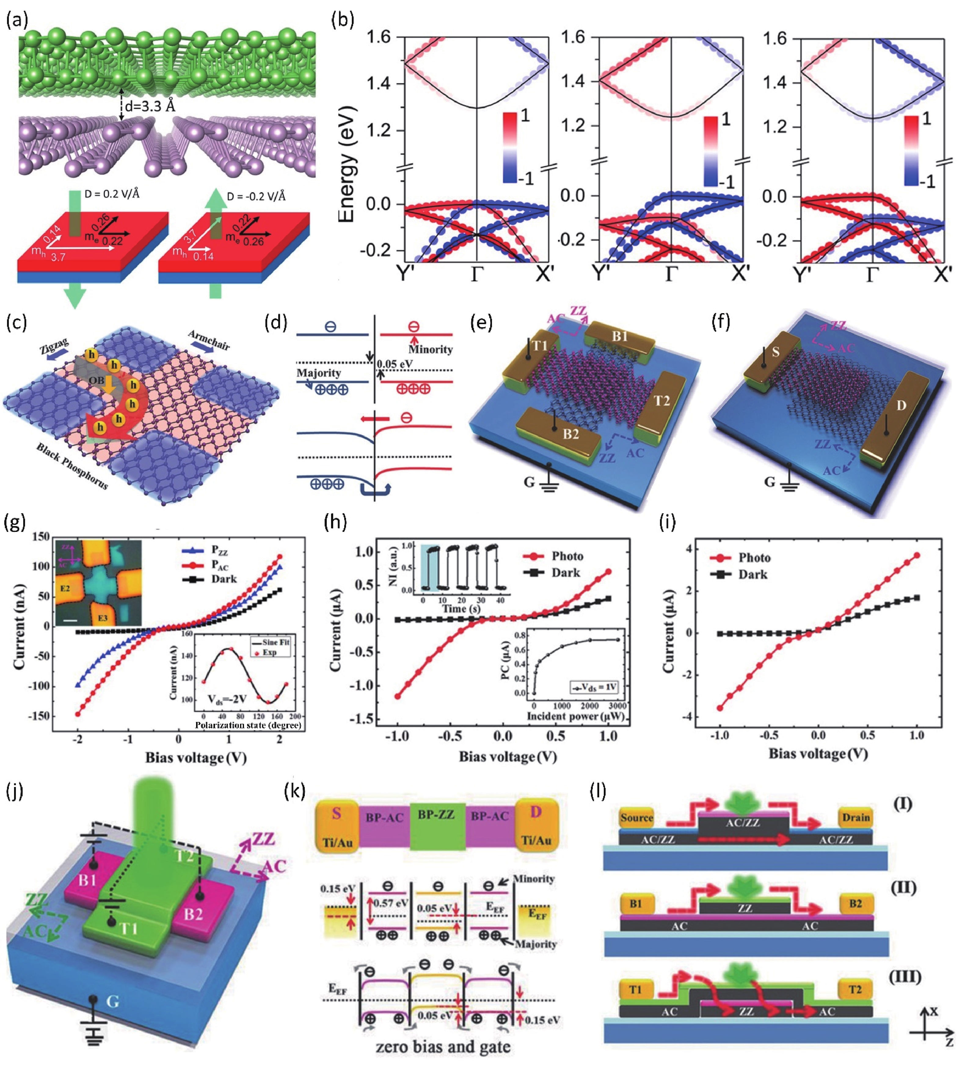
Twist-angle two-dimensional systems, such as twisted bilayer graphene, twisted bilayer transition metal dichalcogenides, twisted bilayer phosphorene and their multilayer van der Waals heterostructures, exhibit novel and tunable properties due to the formation of Moiré superlattice and modulated Moiré bands. The review presents a brief venation on the development of “twistronics” and subsequent applications based on band engineering by twisting. Theoretical predictions followed by experimental realization of magic-angle bilayer graphene ignited the flame of investigation on the new freedom degree, twist-angle, to adjust (opto)electrical behaviors. Then, the merging of Dirac cones and the presence of flat bands gave rise to enhanced light-matter interaction and gate-dependent electrical phases, respectively, leading to applications in photodetectors and superconductor electronic devices. At the same time, the increasing amount of theoretical simulation on extended twisted 2D materials like TMDs and BPs called for further experimental verification. Finally, recently discovered properties in twisted bilayer h-BN evidenced h-BN could be an ideal candidate for dielectric and ferroelectric devices. Hence, both the predictions and confirmed properties imply twist-angle two-dimensional superlattice is a group of promising candidates for next-generation (opto)electronics.


J. Semicond.
2022, 43(1): 013101 doi: 10.1088/1674-4926/43/1/013101

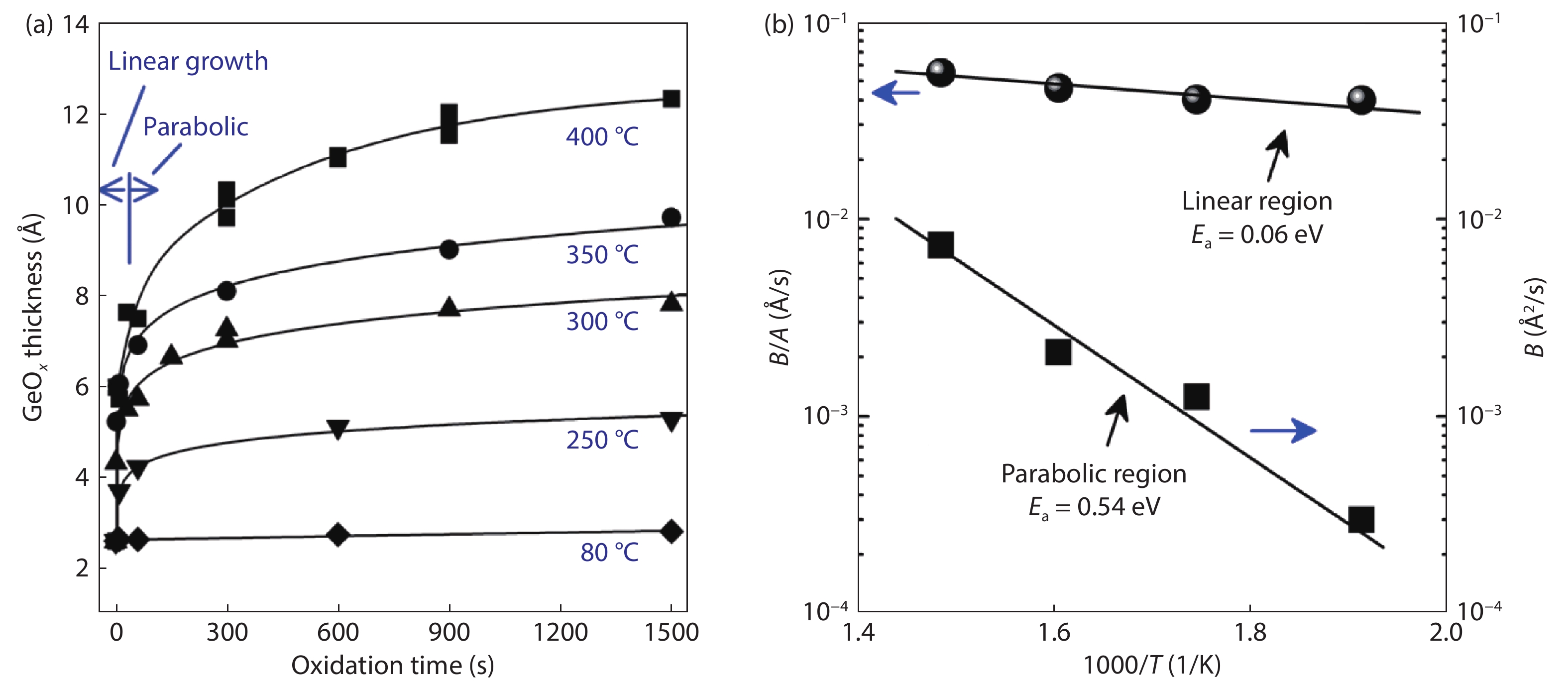
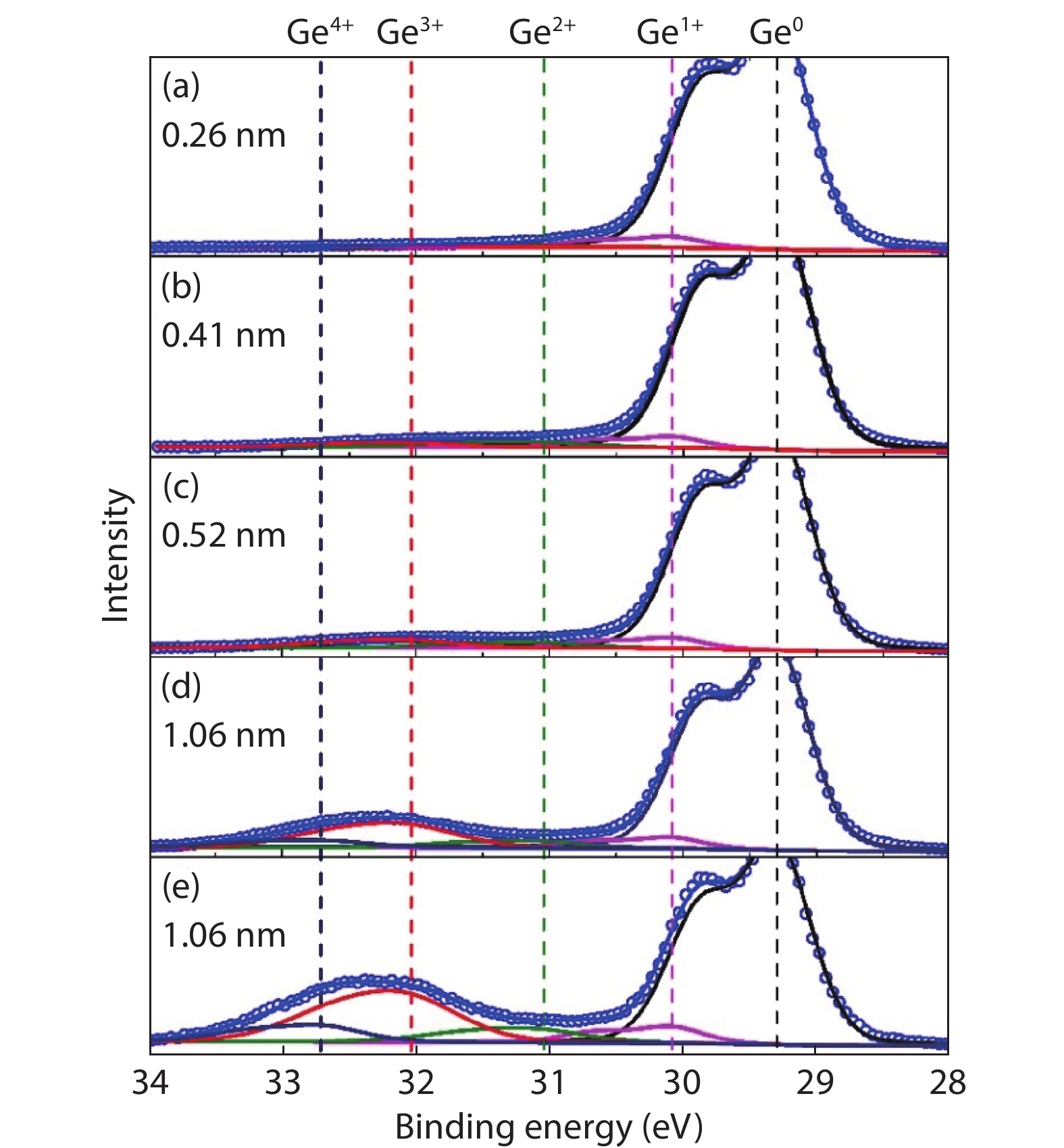
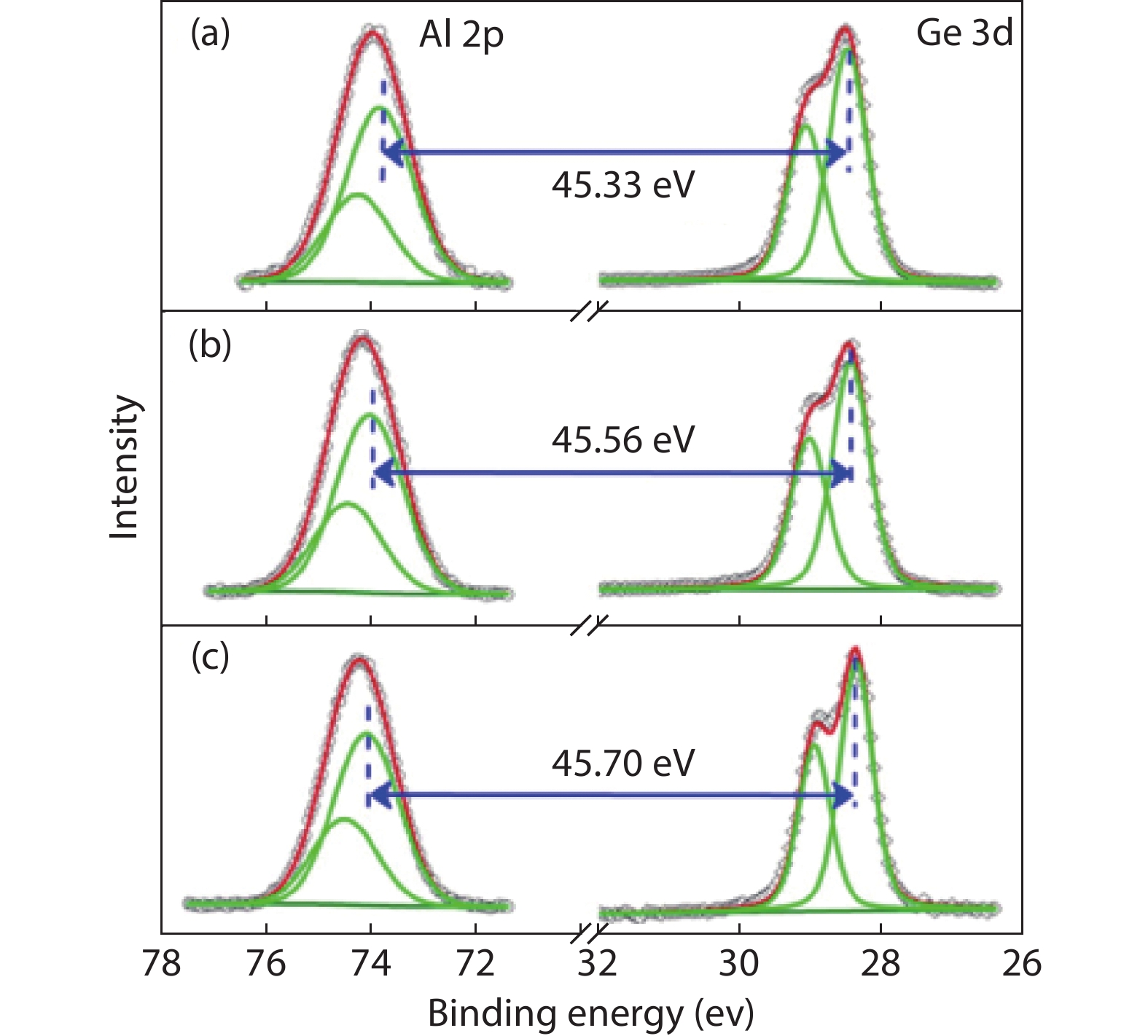
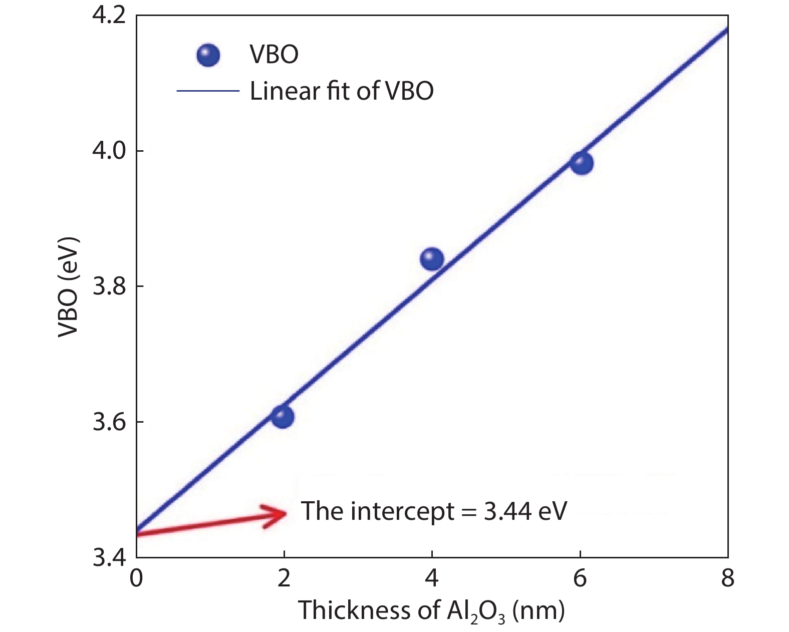
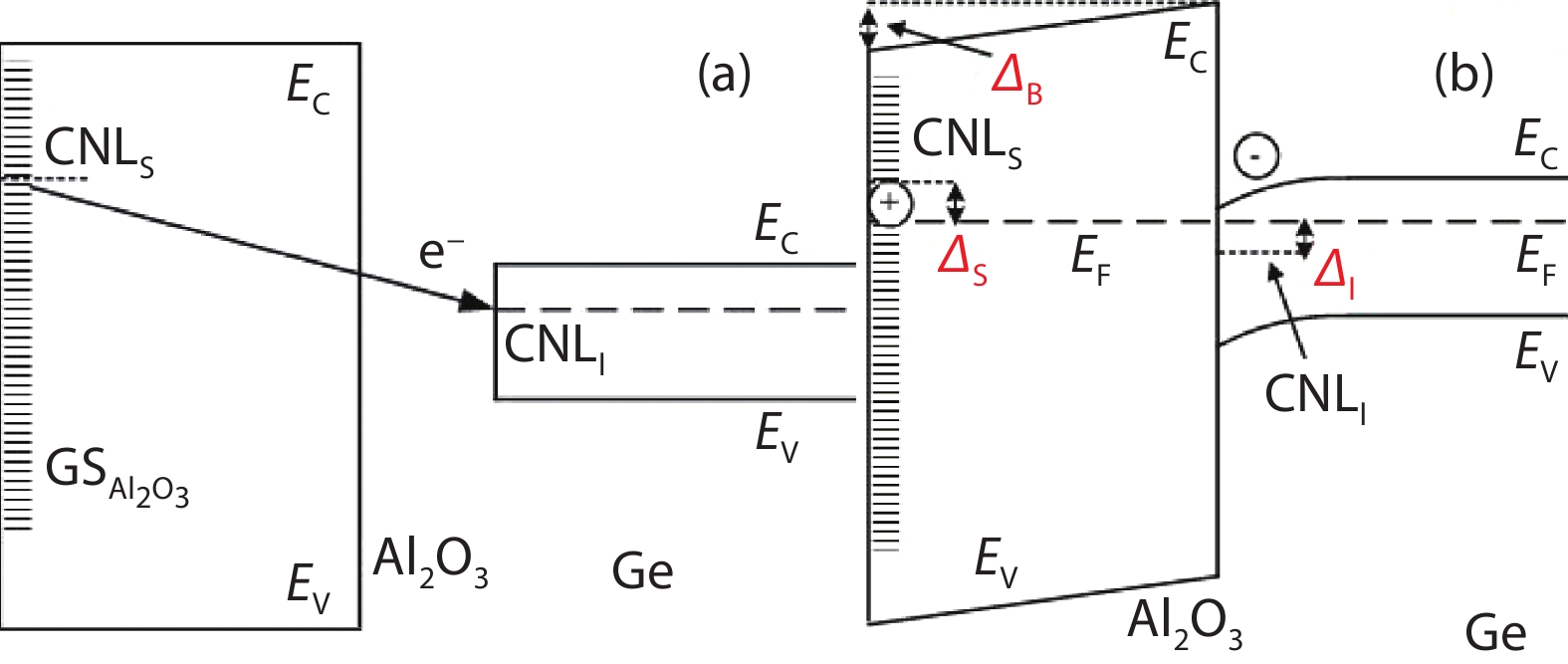
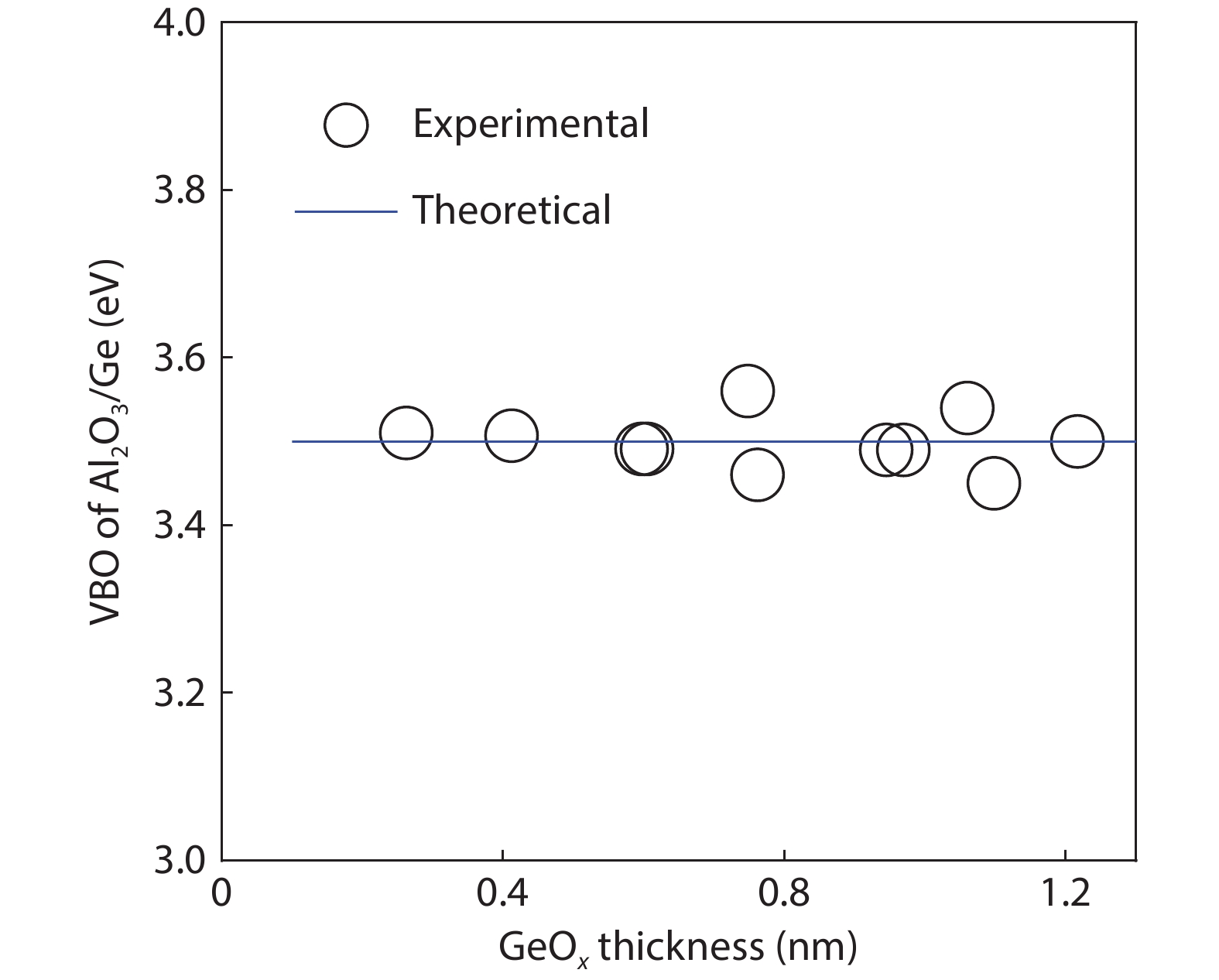
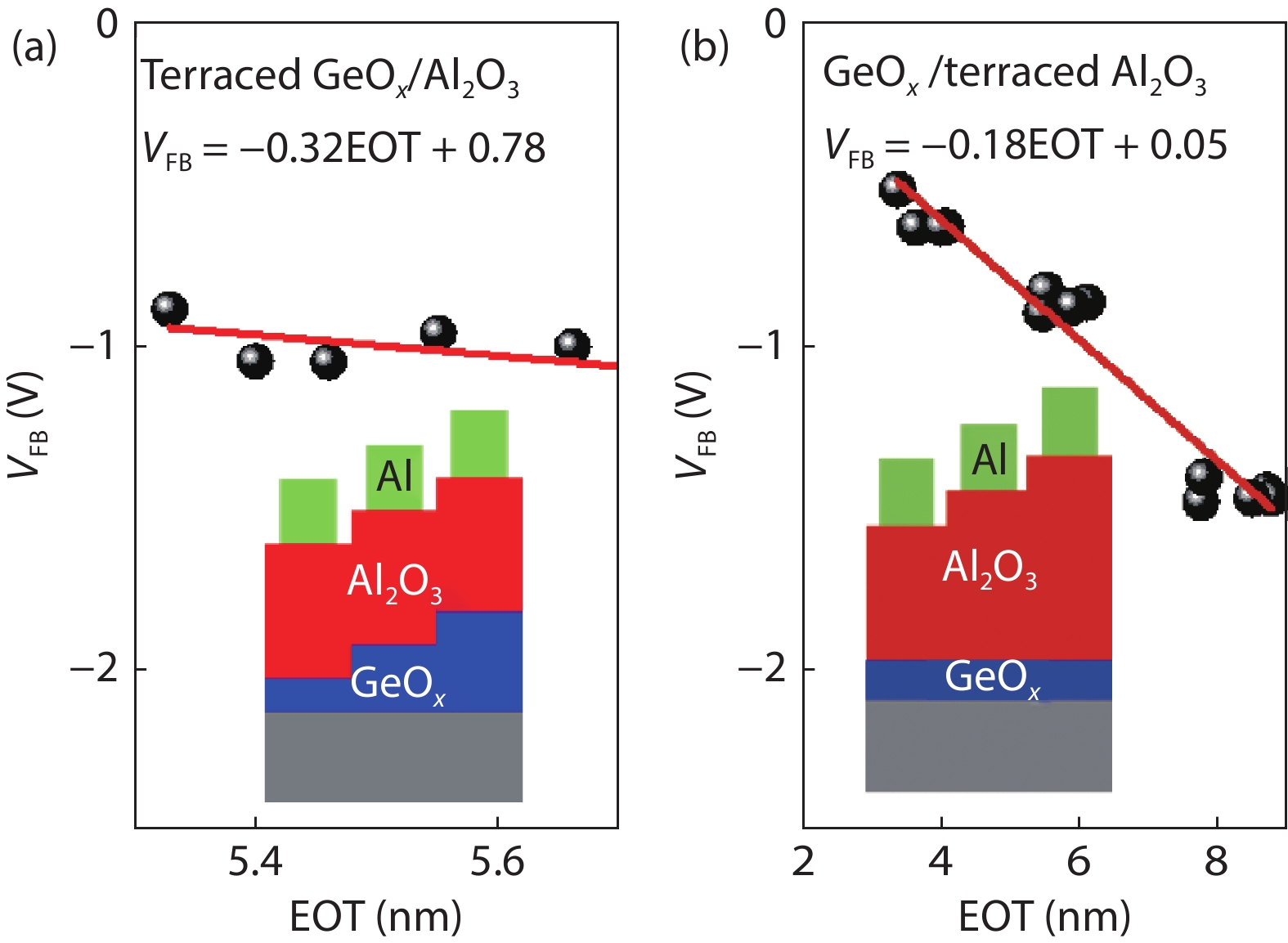
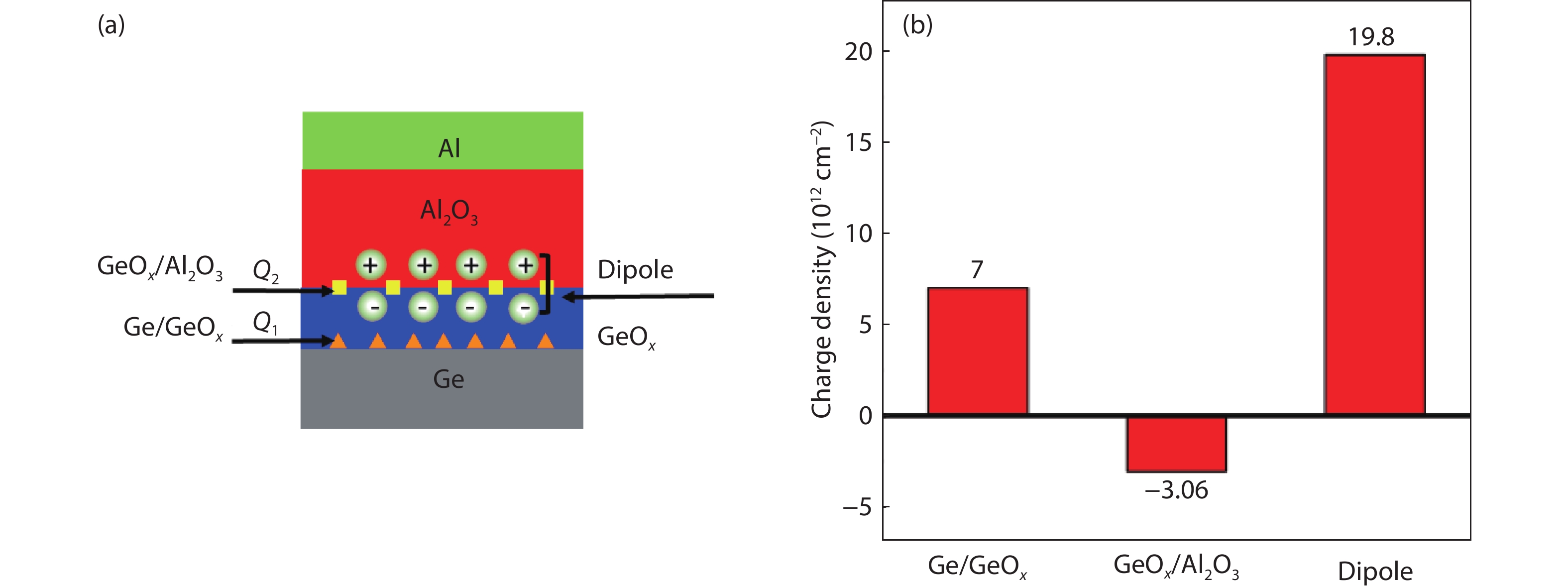
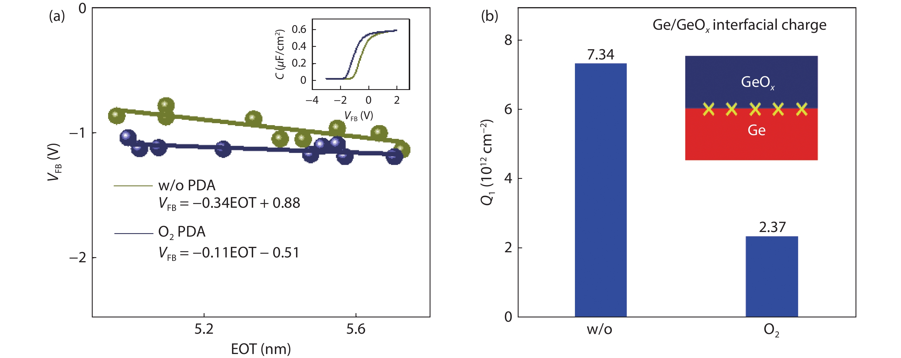
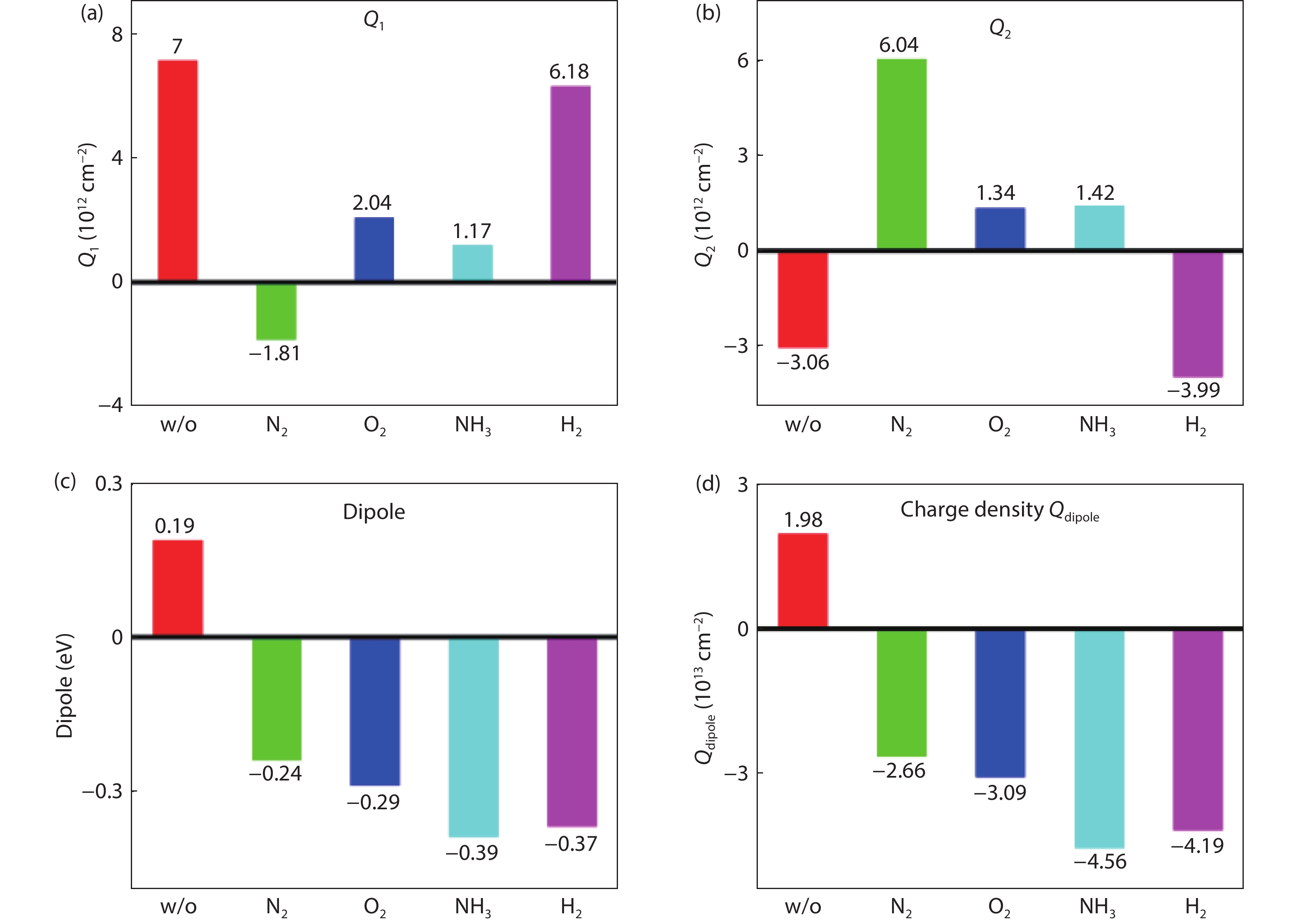
Ge has been an alternative channel material for the performance enhancement of complementary metal–oxide–semiconductor (CMOS) technology applications because of its high carrier mobility and superior compatibility with Si CMOS technology. The gate structure plays a key role on the electrical property. In this paper, the property of Ge MOSFET with Al2O3/GeOx/Ge stack by ozone oxidation is reviewed. The GeOx passivation mechanism by ozone oxidation and band alignment of Al2O3/GeOx/Ge stack is described. In addition, the charge distribution in the gate stack and remote Coulomb scattering on carrier mobility is also presented. The surface passivation is mainly attributed to the high oxidation state of Ge. The energy band alignment is well explained by the gap state theory. The charge distribution is quantitatively characterized and it is found that the gate charges make a great degradation on carrier mobility. These investigations help to provide an impressive understanding and a possible instructive method to improve the performance of Ge devices.


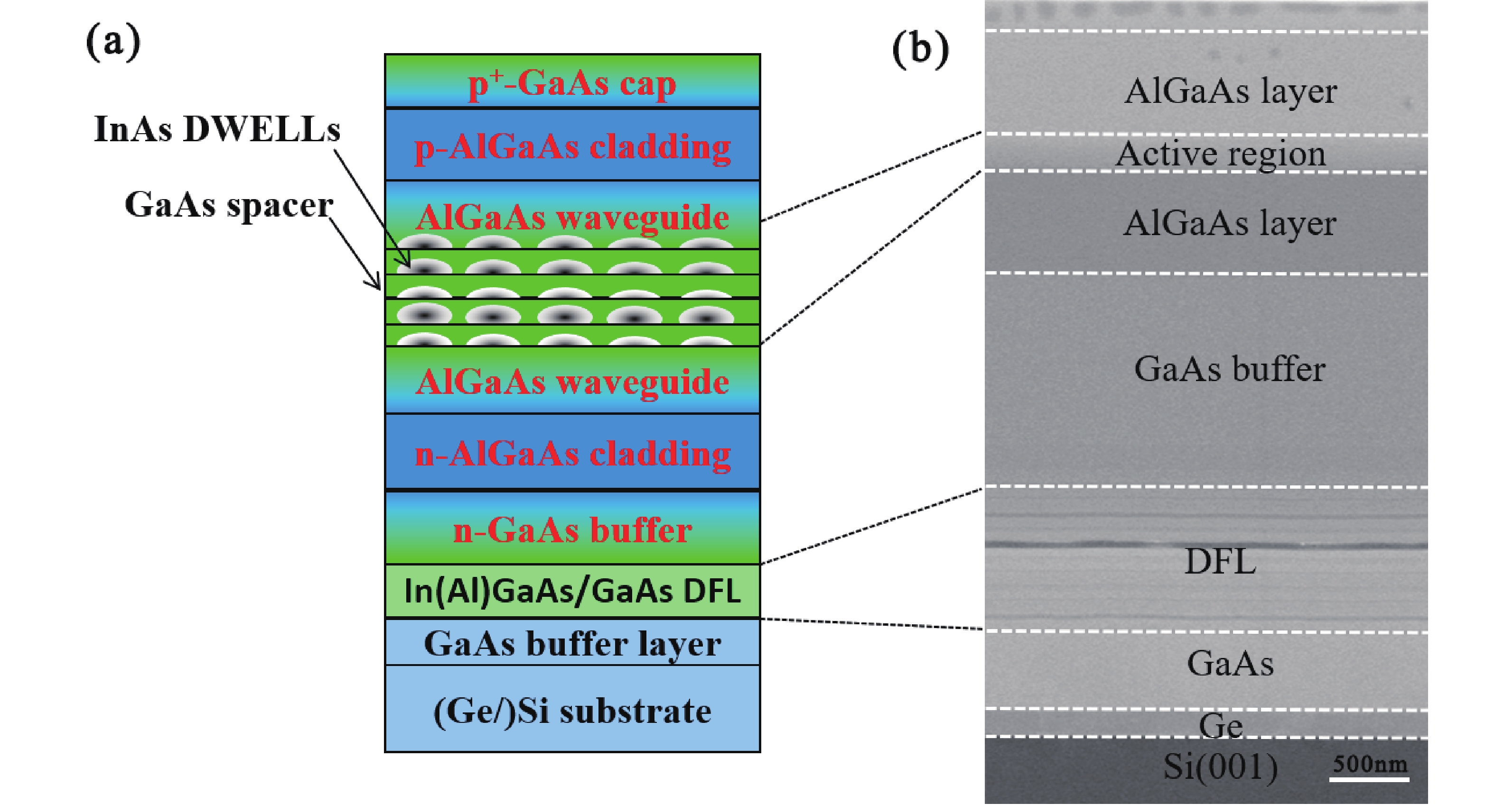
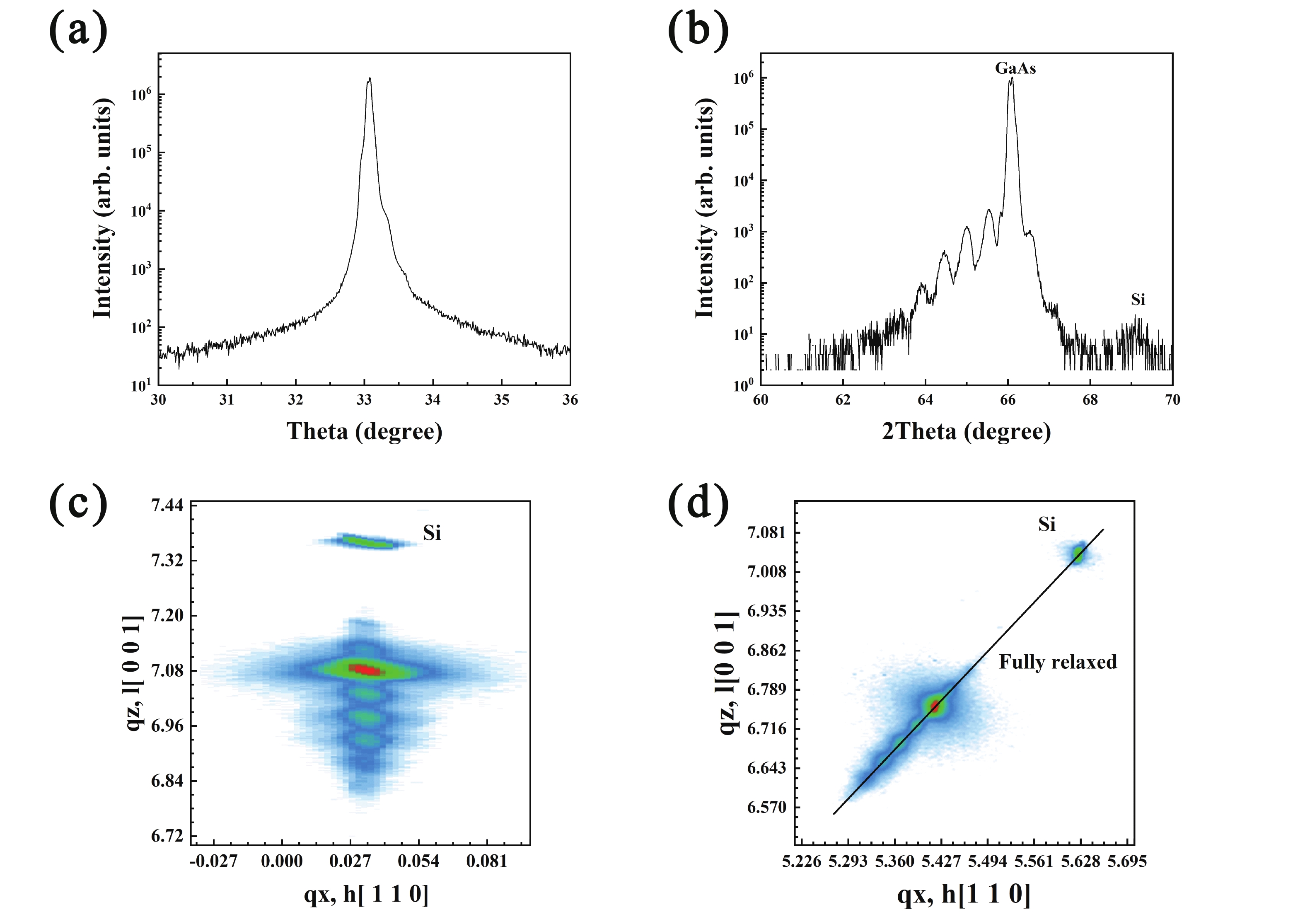
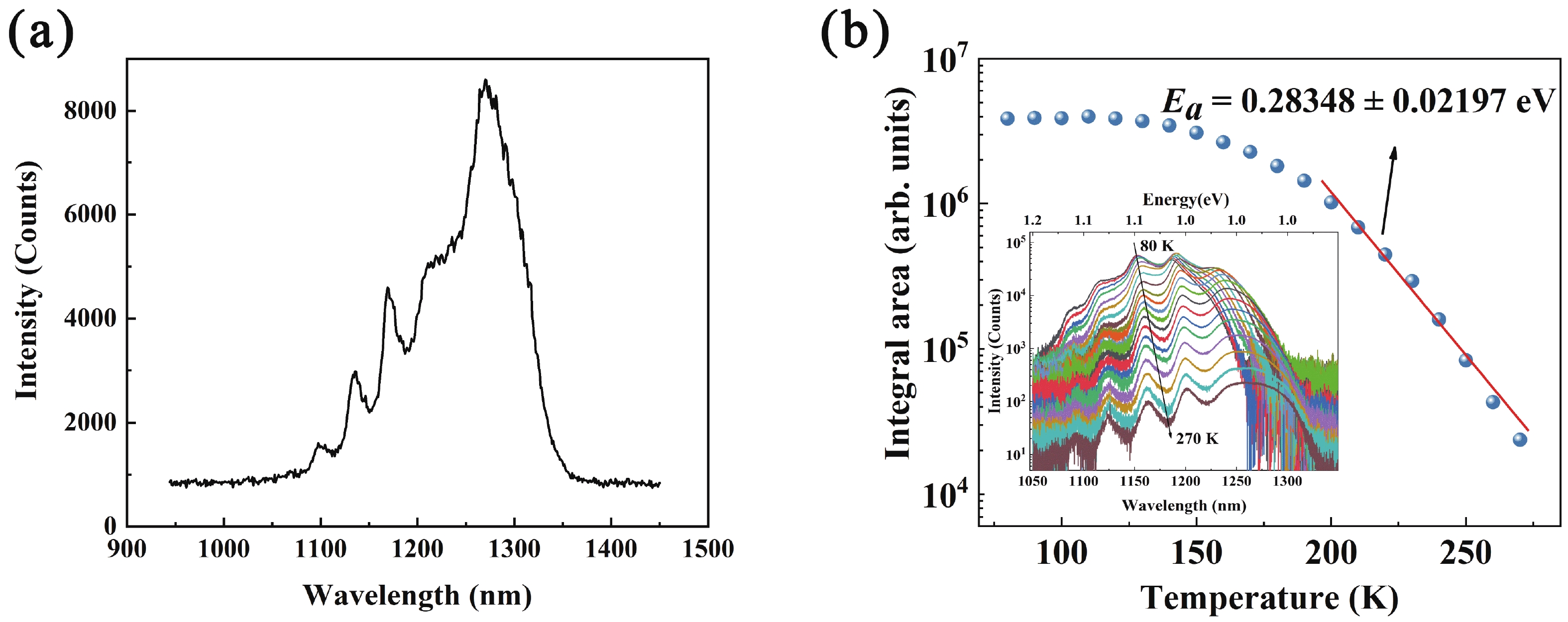
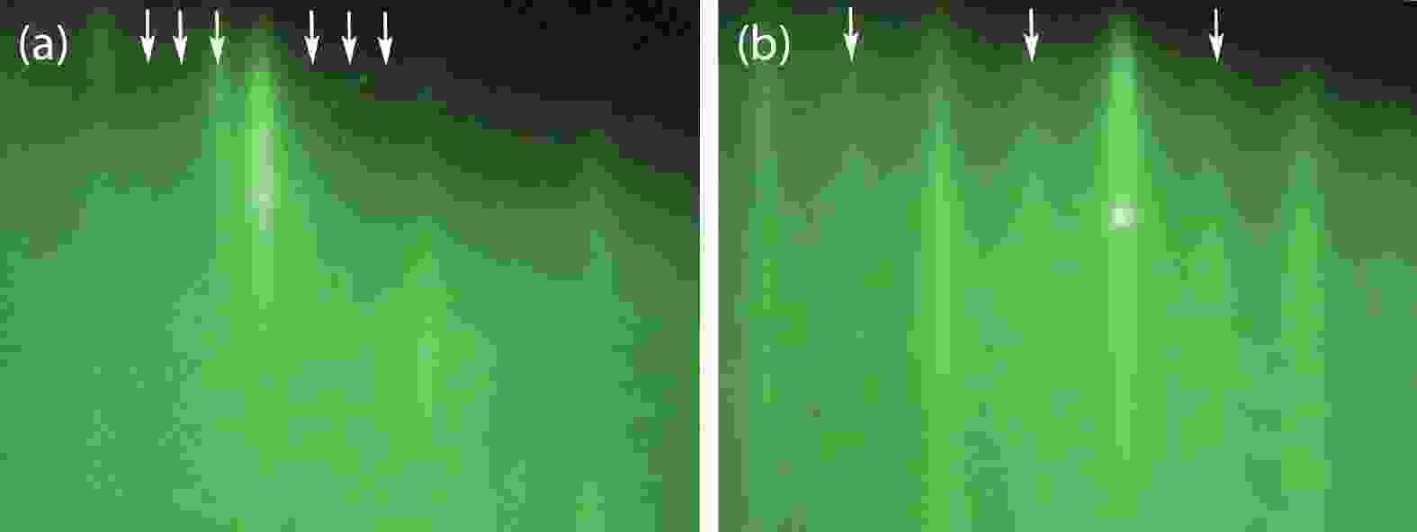
Investigation into the InAs/GaAs quantum dot material epitaxially grown on silicon for O band lasers
J. Semicond.
2022, 43(1): 012301 doi: 10.1088/1674-4926/43/1/012301
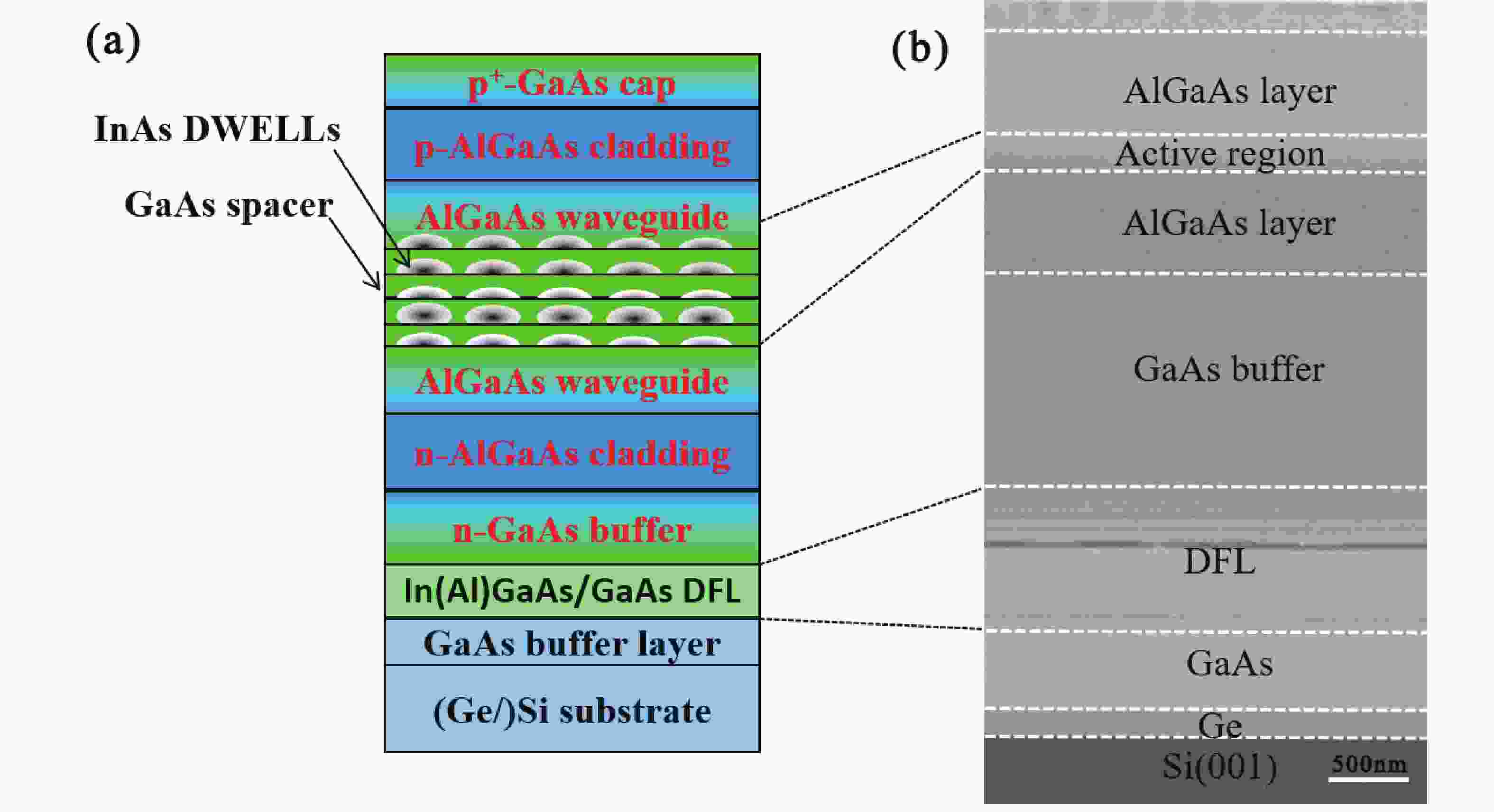
InAs/GaAs quantum dot (QD) lasers were grown on silicon substrates using a thin Ge buffer and three-step growth method in the molecular beam epitaxy (MBE) system. In addition, strained superlattices were used to prevent threading dislocations from propagating to the active region of the laser. The as-grown material quality was characterized by the transmission electron microscope, scanning electron microscope, X-ray diffraction, atomic force microscope, and photoluminescence spectroscopy. The results show that a high-quality GaAs buffer with few dislocations was obtained by the growth scheme we developed. A broad-area edge-emitting laser was also fabricated. The O-band laser exhibited a threshold current density of 540 A/cm2 at room temperature under continuous wave conditions. This work demonstrates the potential of large-scale and low-cost manufacturing of the O-band InAs/GaAs quantum dot lasers on silicon substrates.


J. Semicond.
2022, 43(1): 012302 doi: 10.1088/1674-4926/43/1/012302
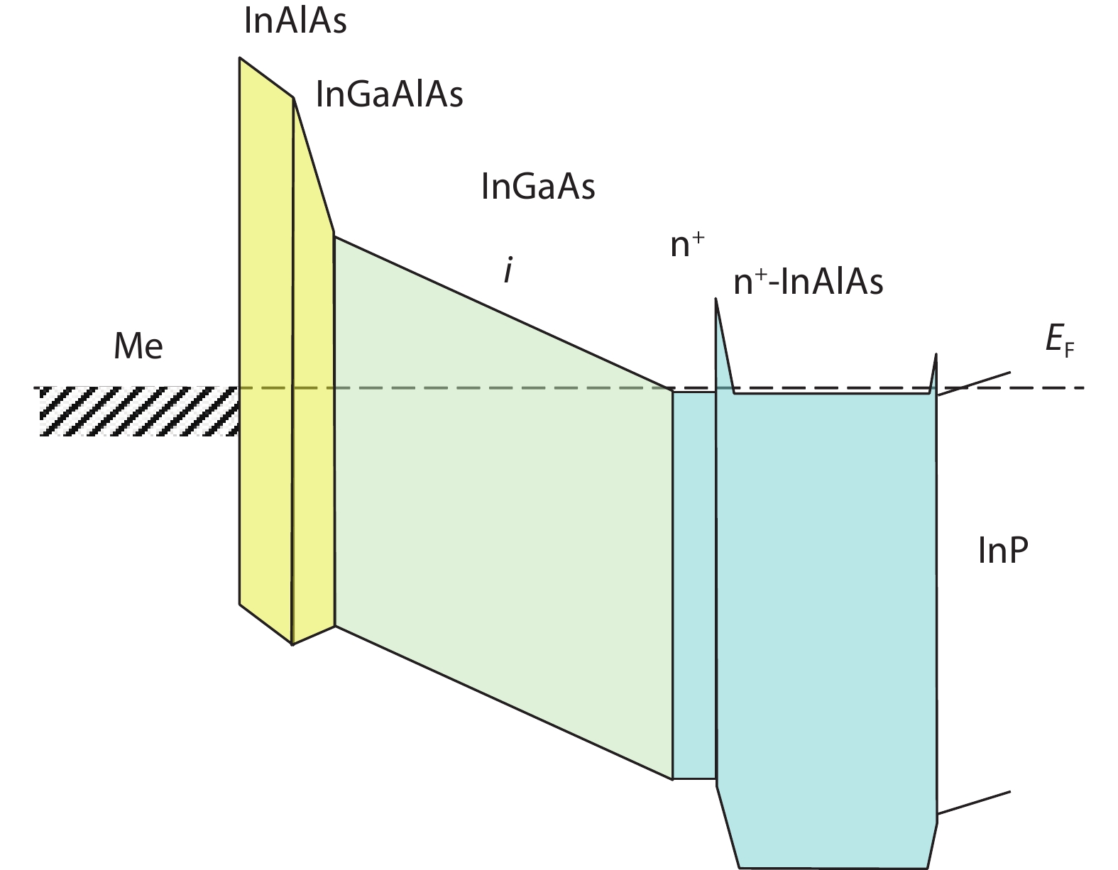
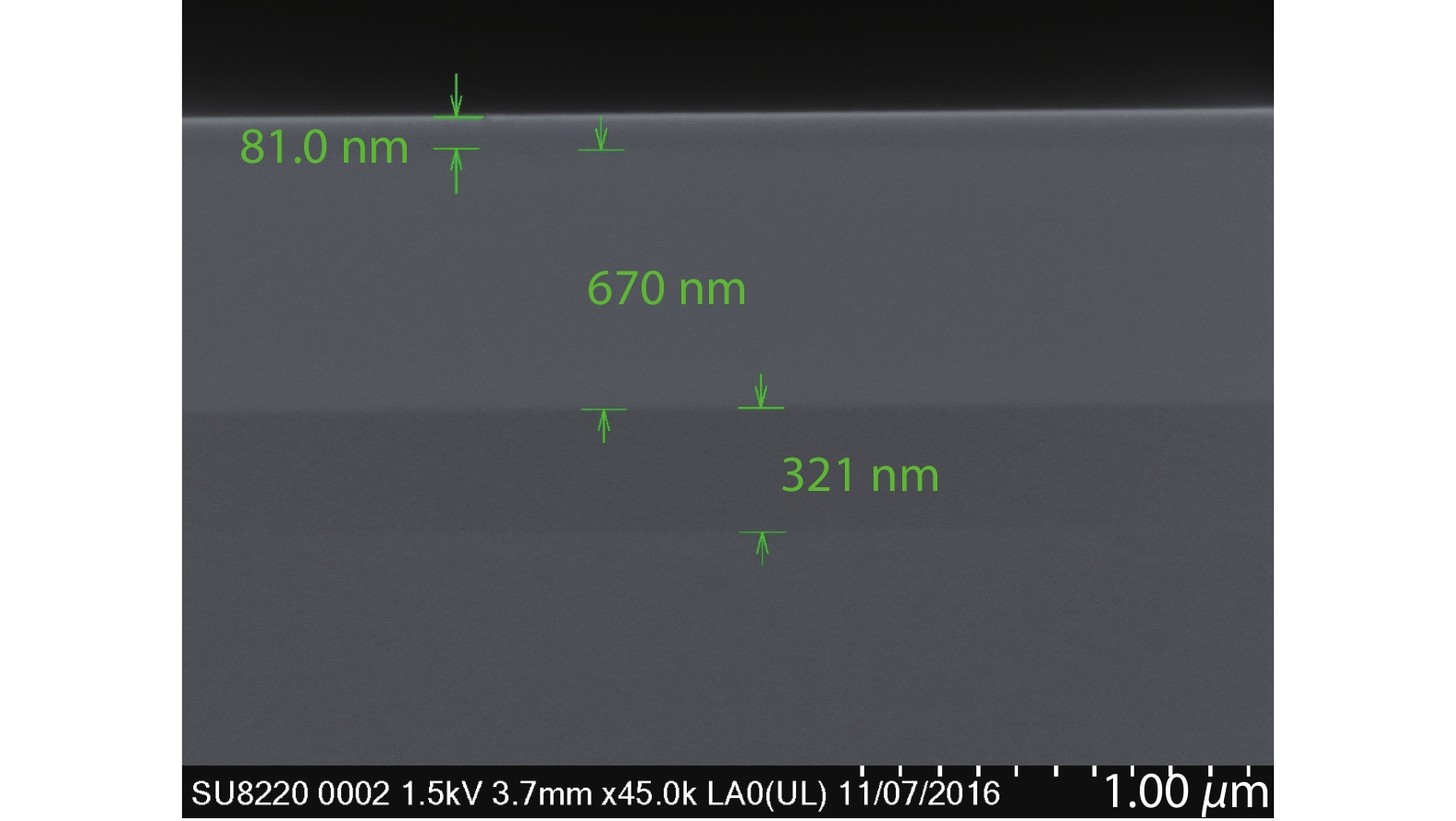
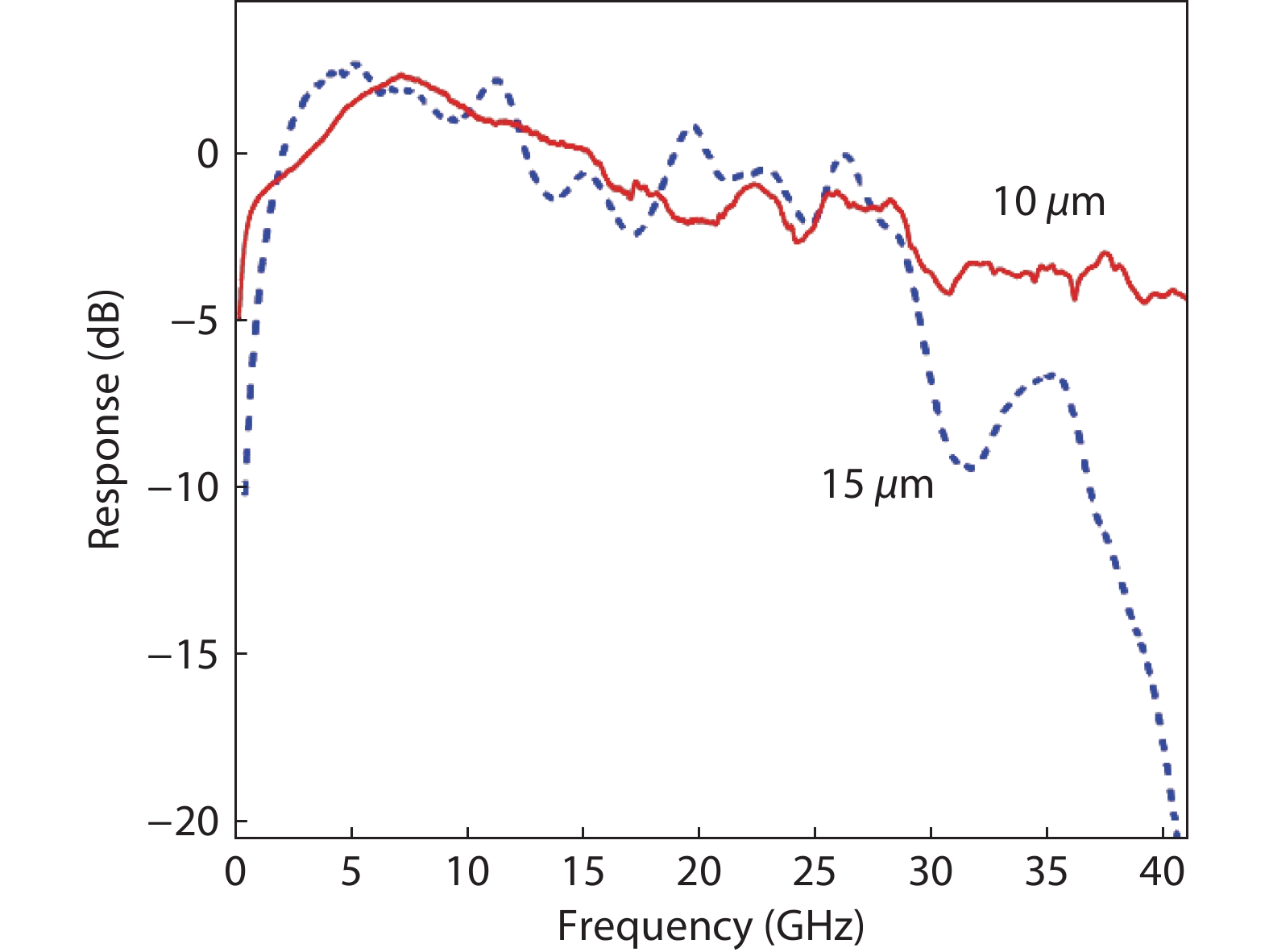
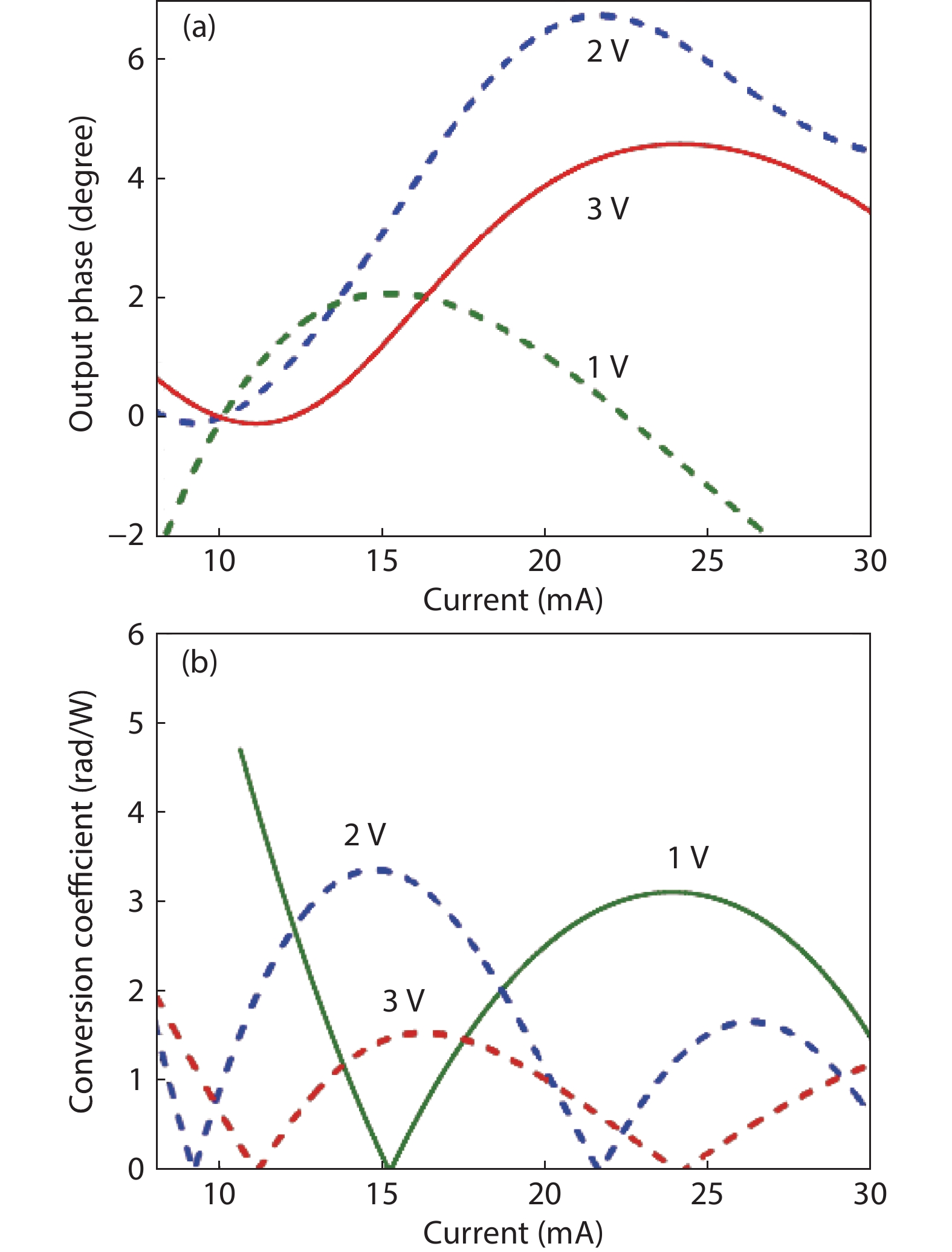
The design, manufacturing and DC and microwave characterization of high-power Schottky barrier InAlAs/InGaAs back-illuminated mesa structure photodiodes are presented. The photodiodes with 10 and 15 μm mesa diameters operate at ≥40 and 28 GHz, respectively, have the output RF power as high as 58 mW at a frequency of 20 GHz, the DC responsivity of up to 1.08 A/W depending on the absorbing layer thickness, and a photodiode dark current as low as 0.04 nA. We show that these photodiodes provide an advantage in the amplitude-to-phase conversion factor which makes them suitable for use in high-speed analog transmission lines with stringent requirements for phase noise.


J. Semicond.
2022, 43(1): 012303 doi: 10.1088/1674-4926/43/1/012303

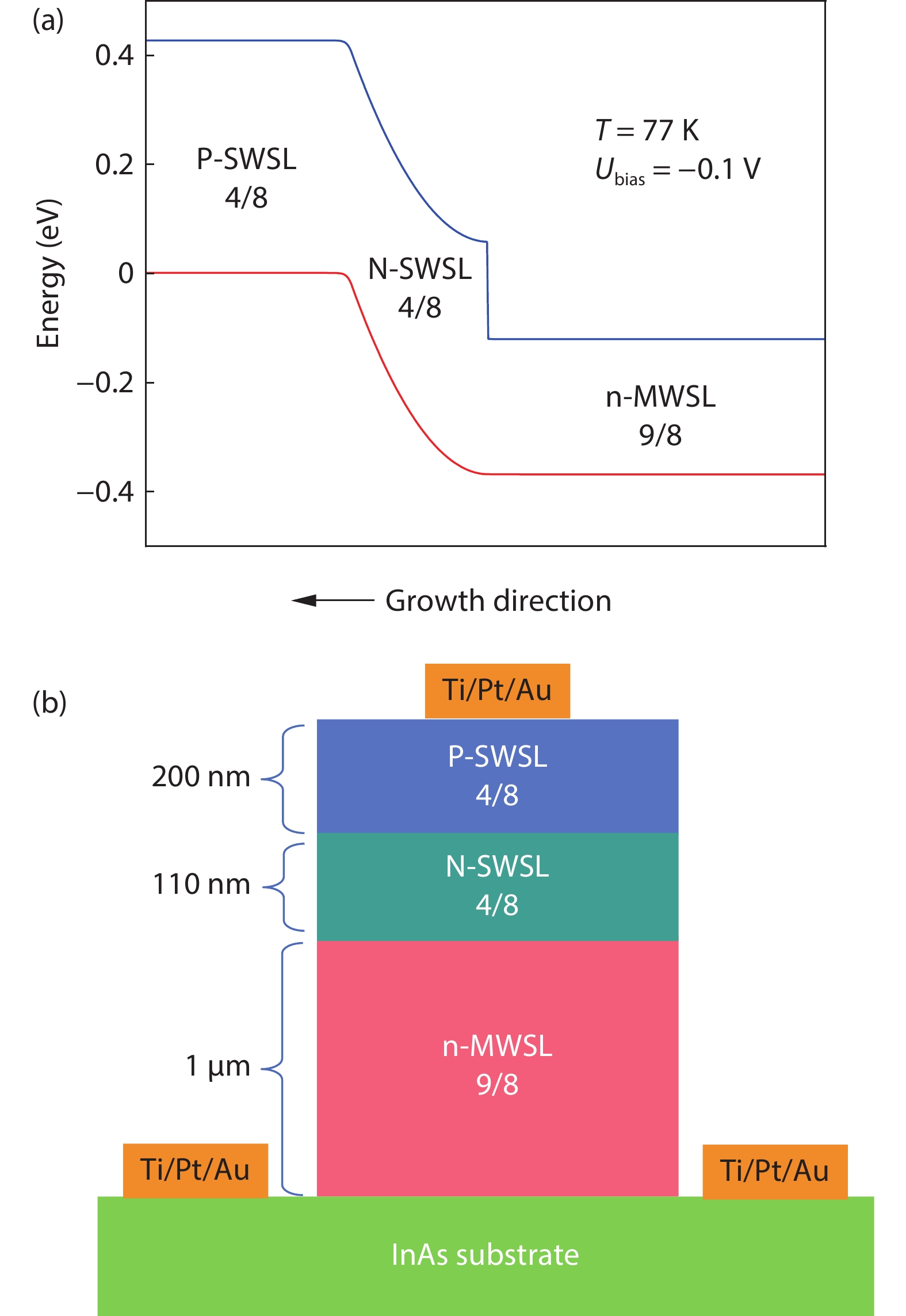
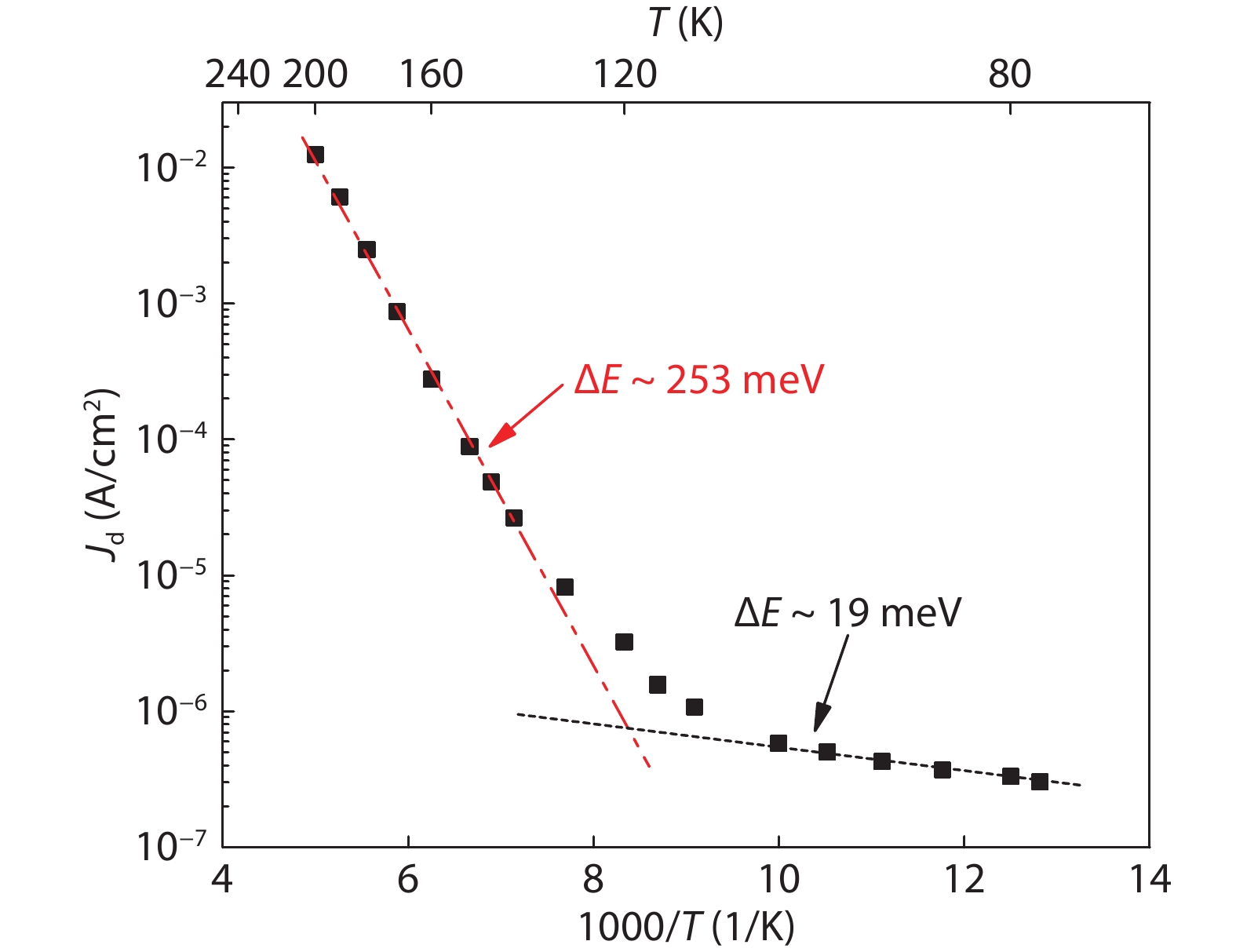
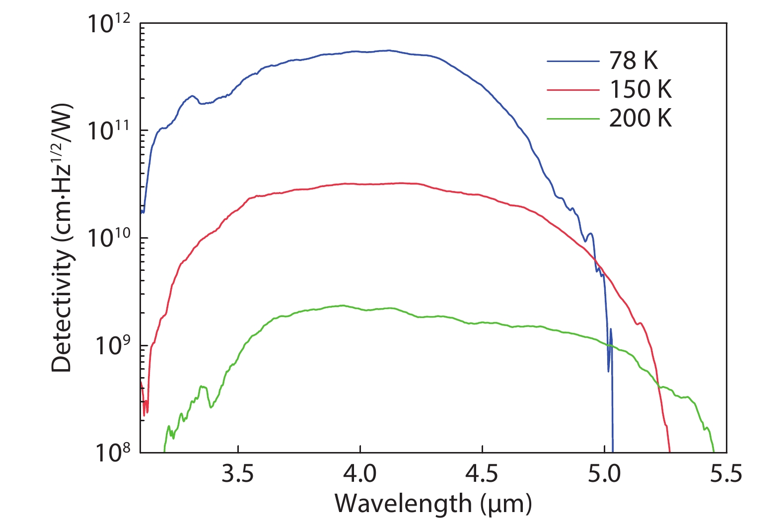
We demonstrate a high-operating-temperature (HOT) mid-wavelength InAs/GaSb superlattice heterojunction infrared photodetector grown by metal–organic chemical vapor deposition. High crystalline quality and the near-zero lattice mismatch of a InAs/GaSb superlattice on an InAs substrate were evidenced by high-resolution X-ray diffraction. At a bias voltage of –0.1 V and an operating temperature of 200 K, the device exhibited a 50% cutoff wavelength of ~ 4.9 μm, a dark current density of 0.012 A/cm2, and a peak specific detectivity of 2.3 × 109 cm·Hz1/2 /W.


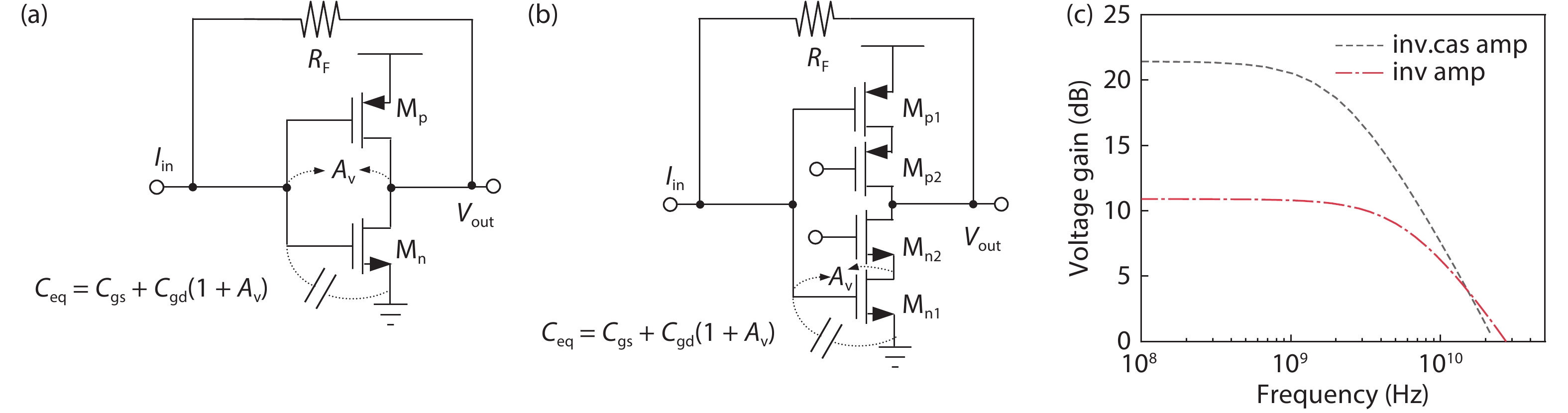
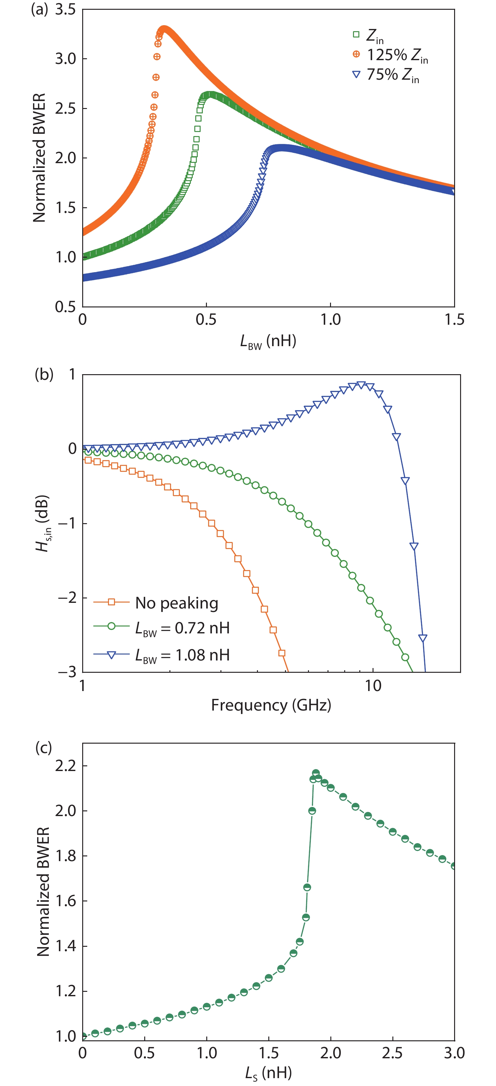
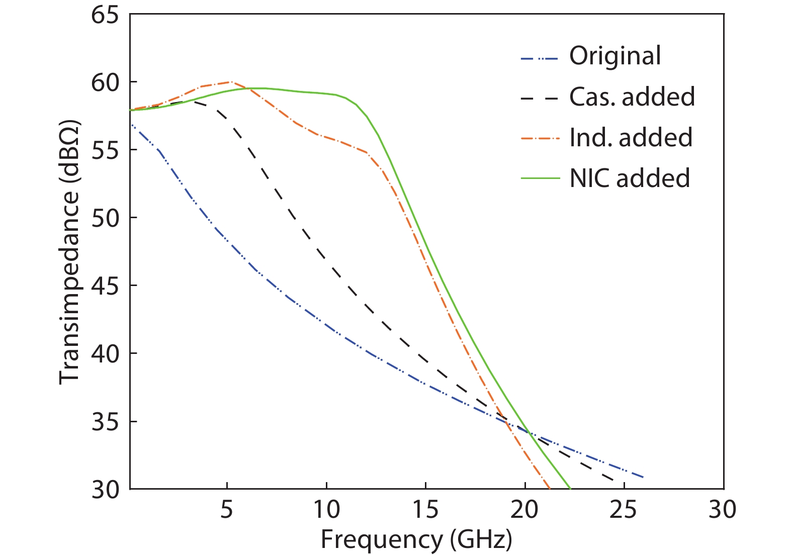
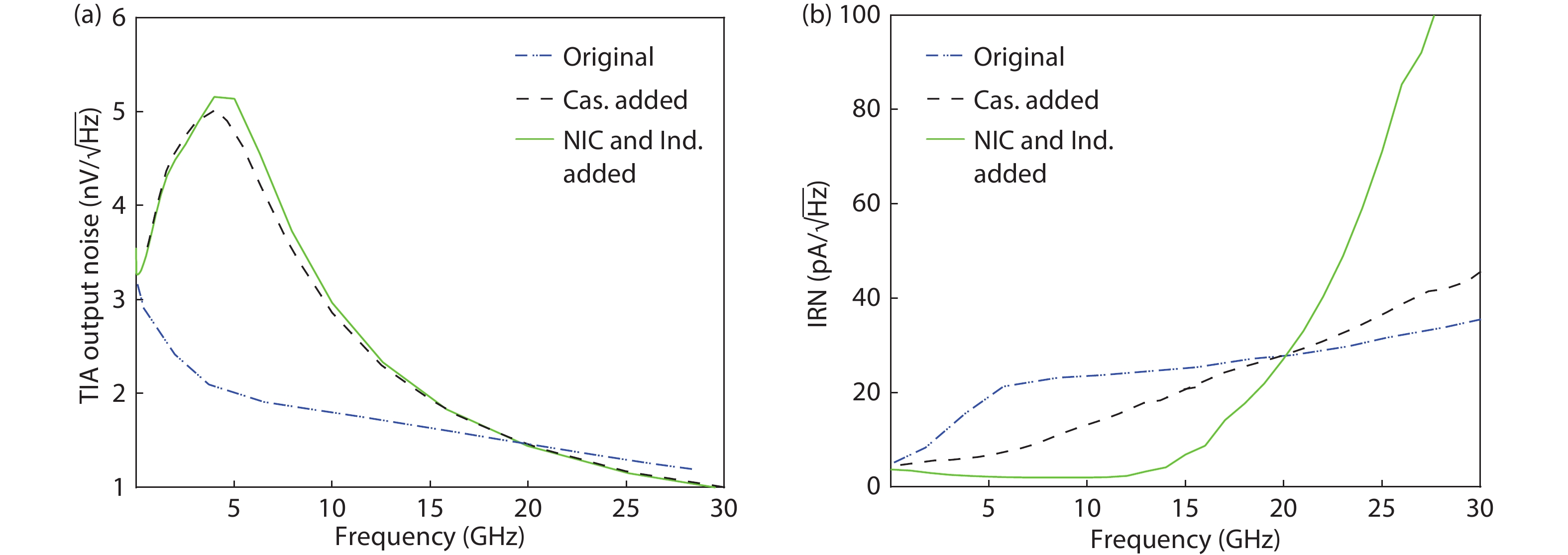
J. Semicond.
2022, 43(1): 012401 doi: 10.1088/1674-4926/43/1/012401
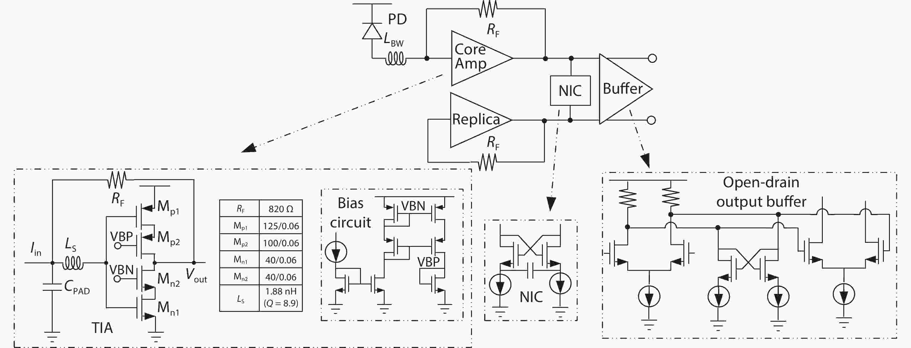
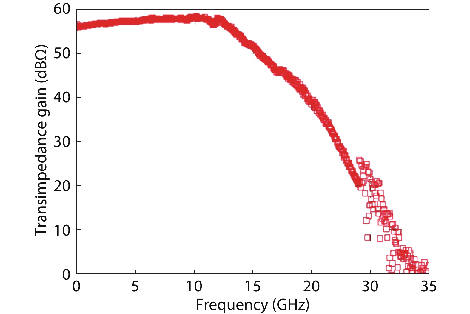
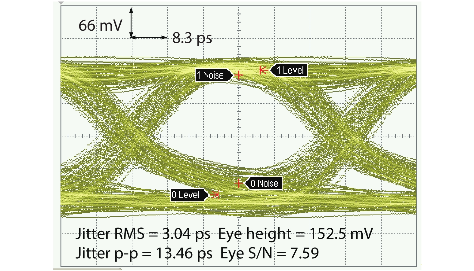
This work presents a high-gain broadband inverter-based cascode transimpedance amplifier fabricated in a 65-nm CMOS process. Multiple bandwidth enhancement techniques, including input bonding wire, input series on-chip inductive peaking and negative capacitance compensation, are adopted to overcome the large off-chip photodiode capacitive loading and the miller capacitance of the input device, achieving an overall bandwidth enhancement ratio of 8.5. The electrical measurement shows TIA achieves 58 dBΩ up to 12.7 GHz with a 180-fF off-chip photodetector. The optical measurement demonstrates a clear open eye of 20 Gb/s. The TIA dissipates 4 mW from a 1.2-V supply voltage.


J. Semicond.
2022, 43(1): 012801 doi: 10.1088/1674-4926/43/1/012801
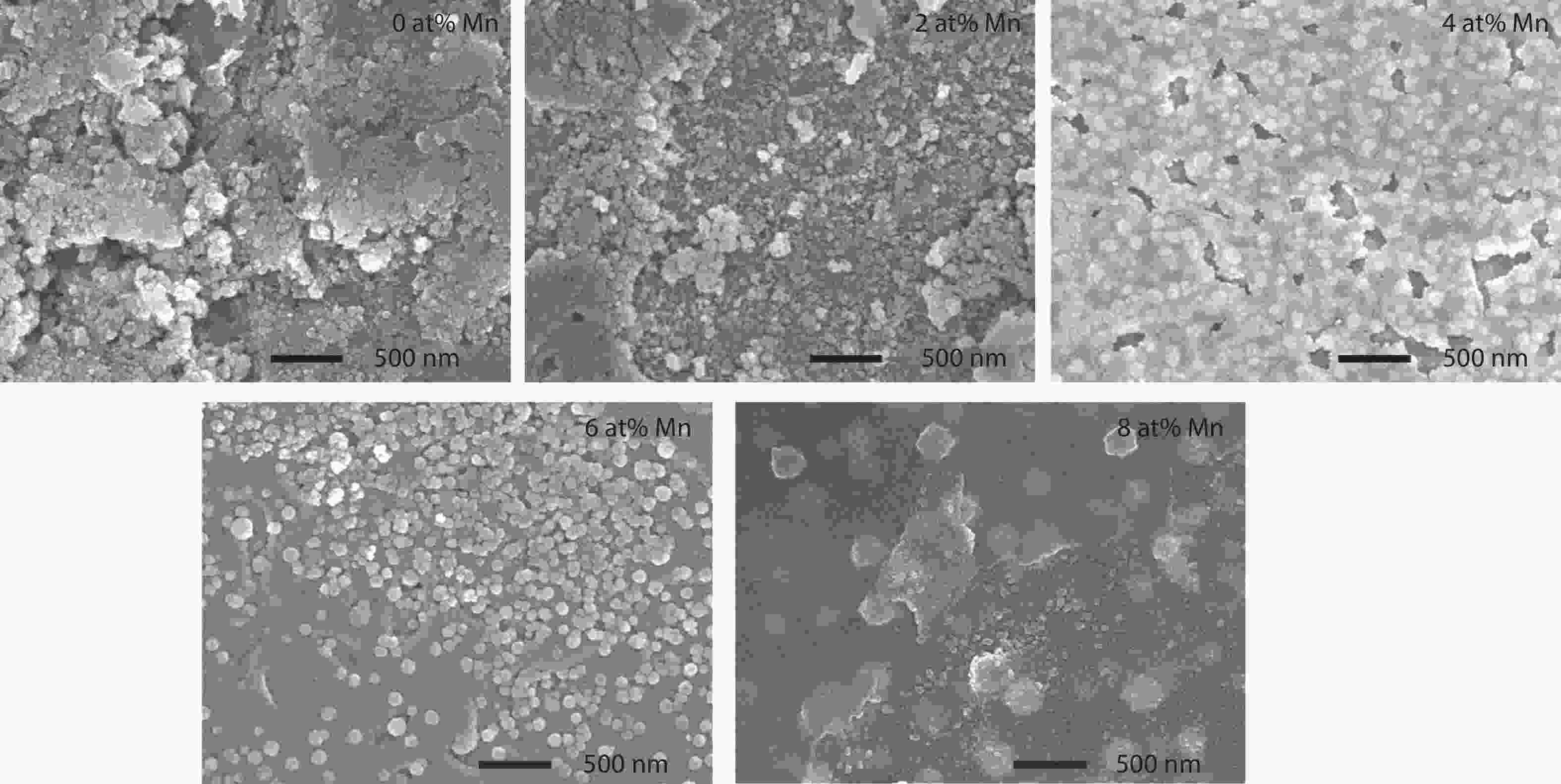
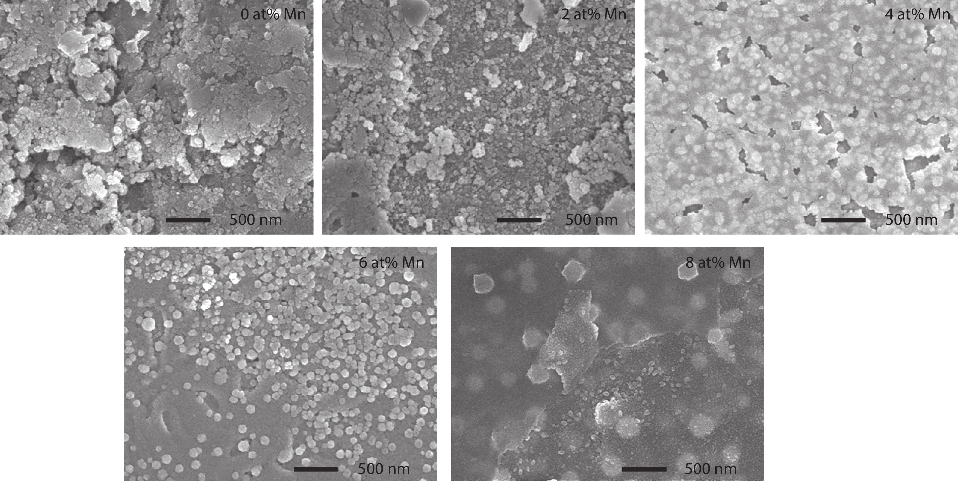
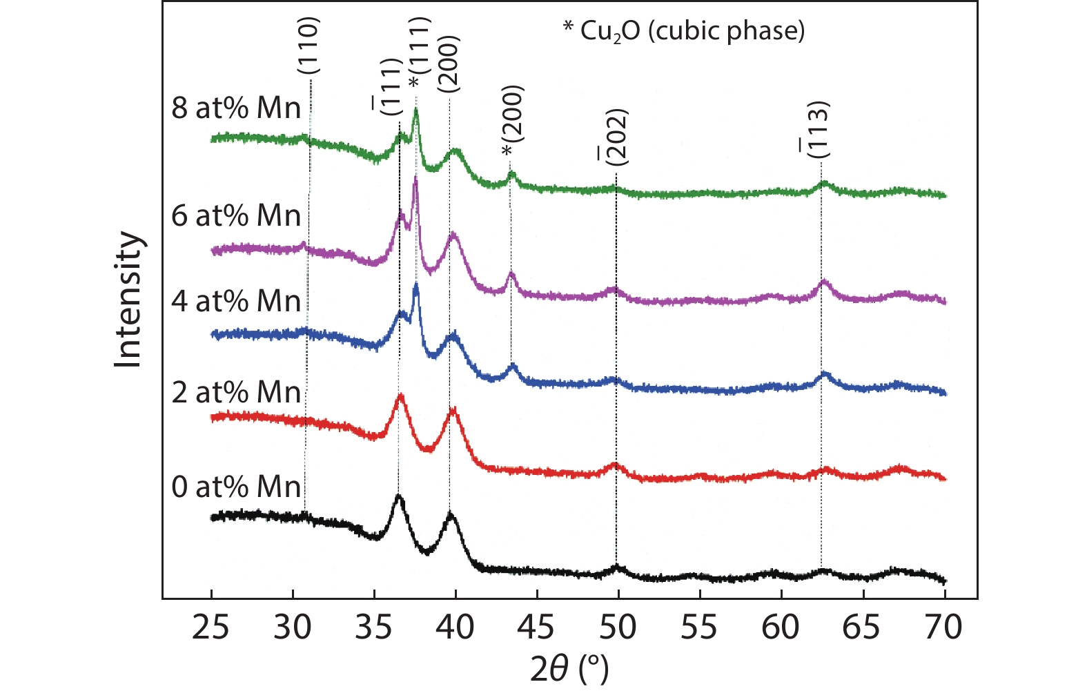
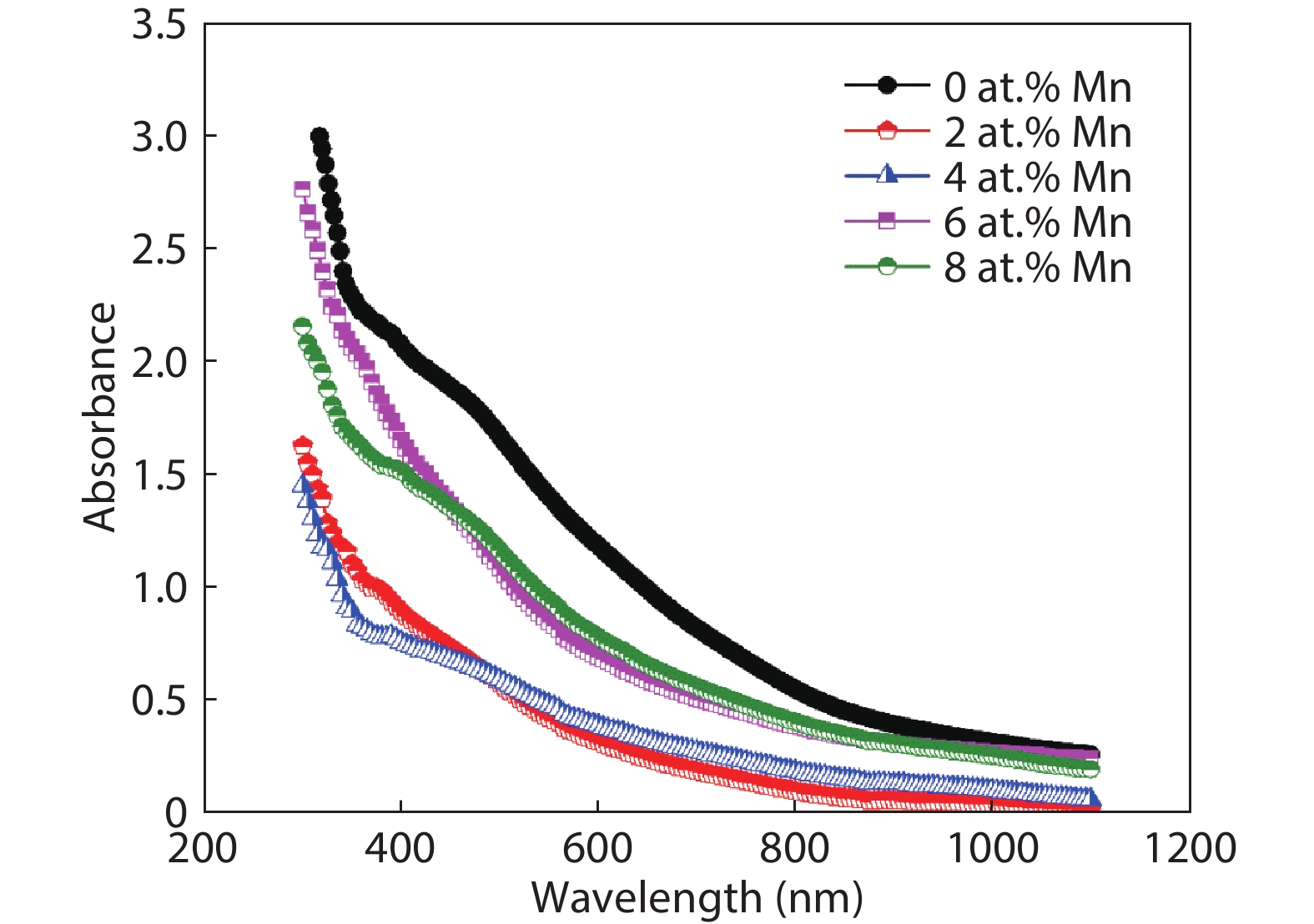
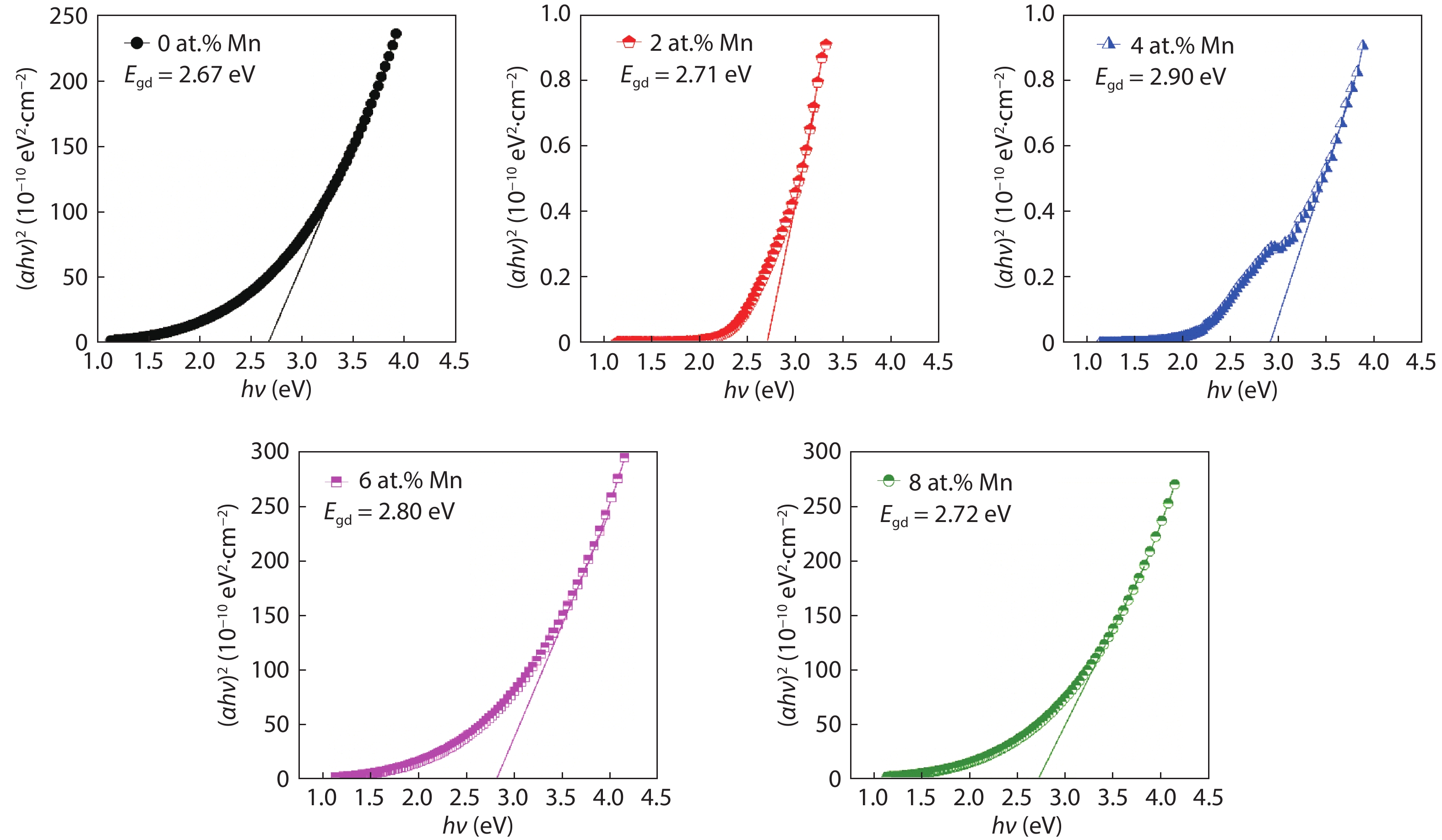
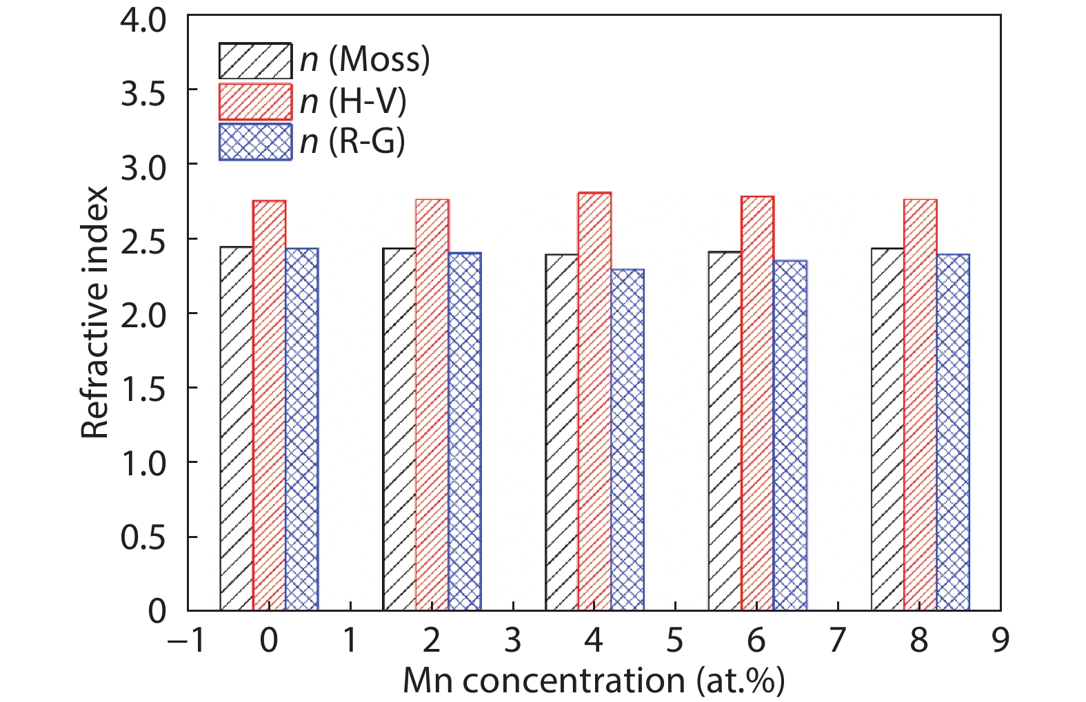
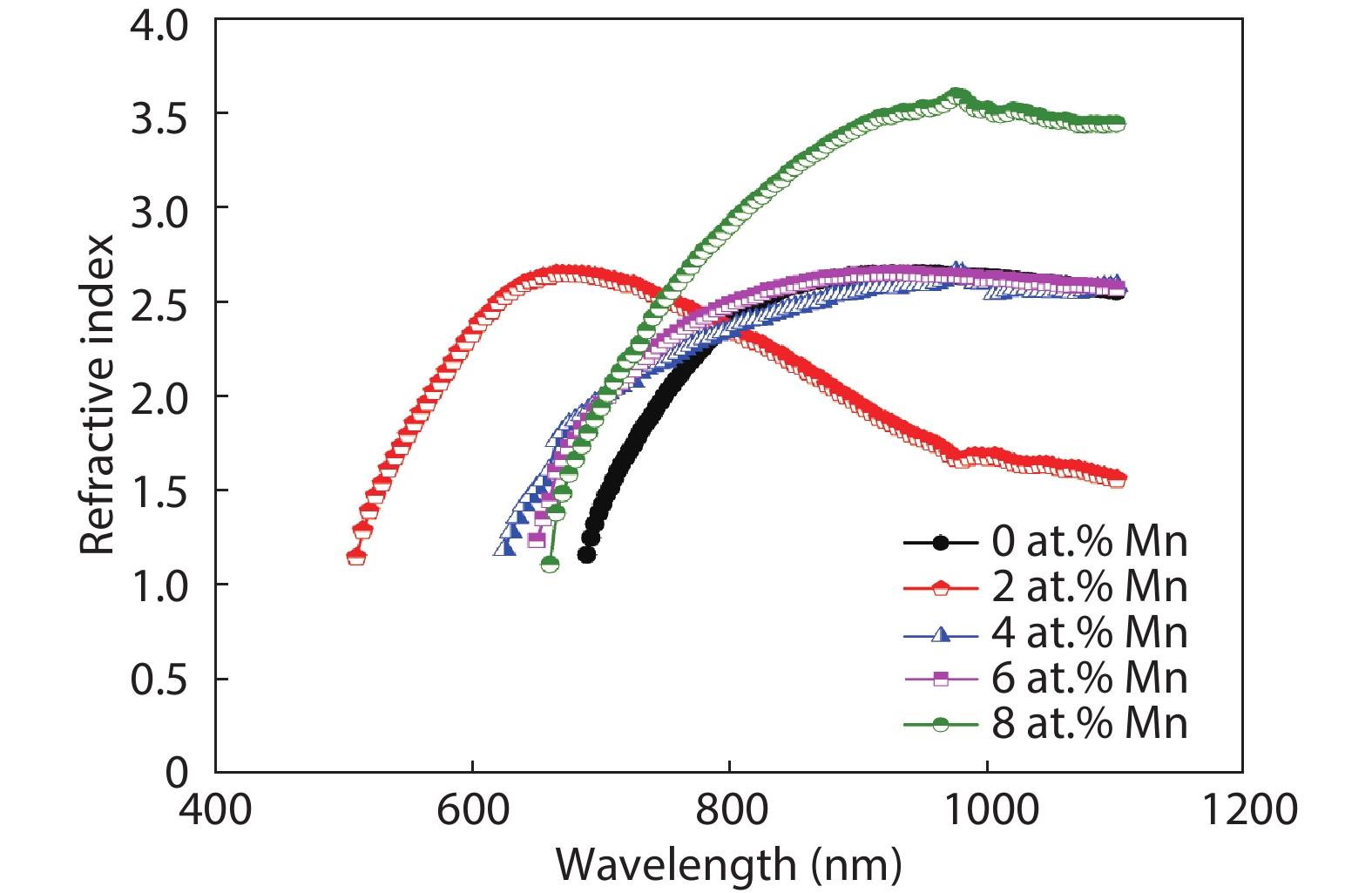
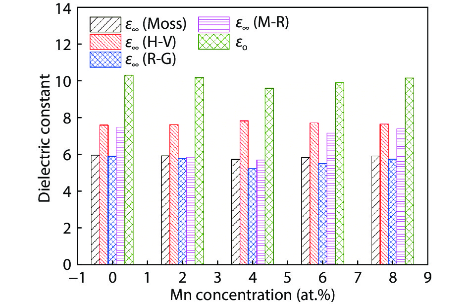
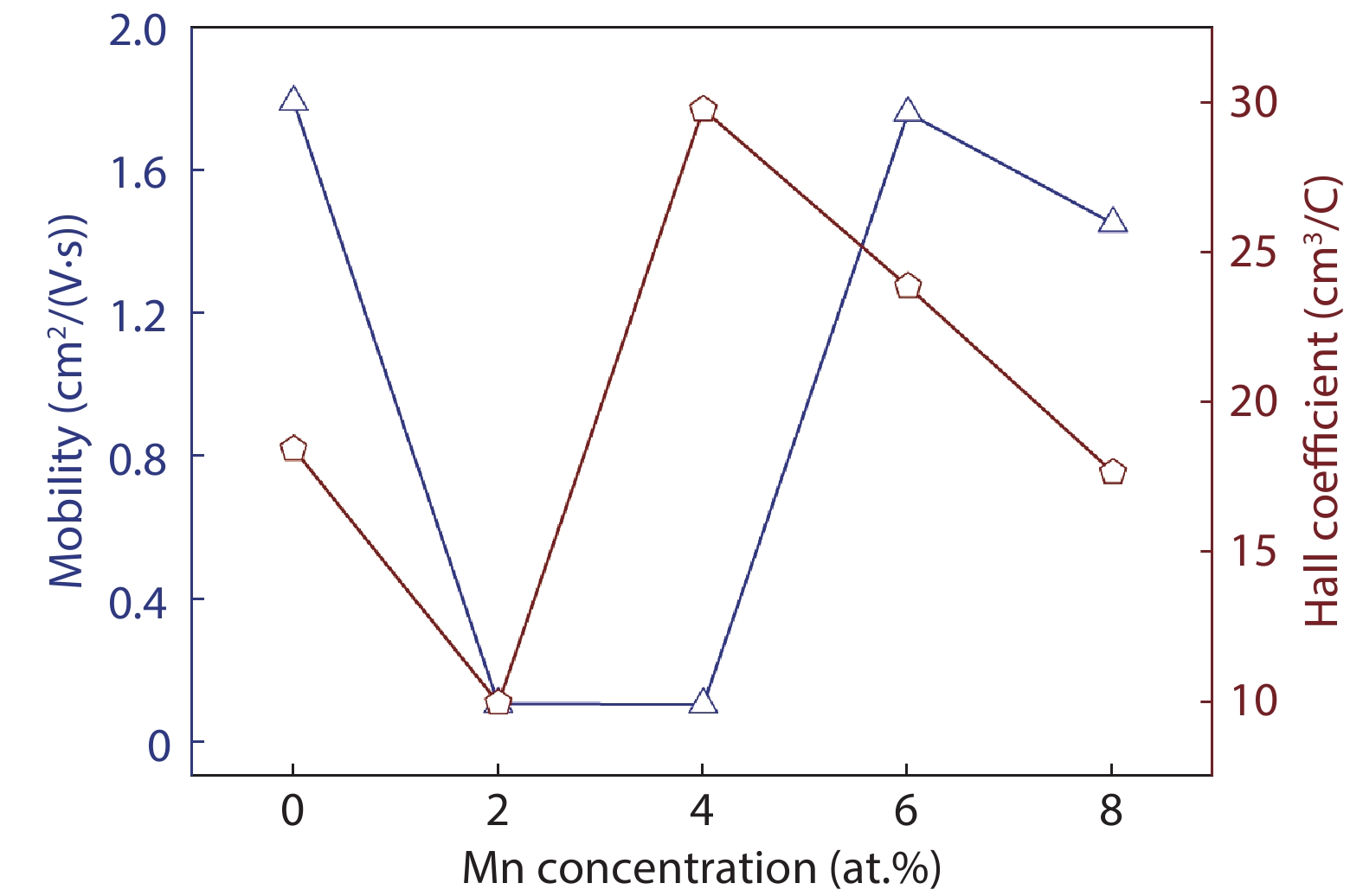
Here we discuss the synthesis of copper (II) oxide (CuO) and manganese (Mn)-doped CuO thin films varying with 0 to 8 at% Mn using the spray pyrolysis technique. As-deposited film surfaces comprised of agglomerated spherical nanoparticles and a semi-spongy porous structure for 4 at% Mn doping. Energy dispersive analysis of X-rays confirmed the chemical composition of the films. X-ray diffraction spectra showed a polycrystalline monoclinic structure with the predominance of the (


J. Semicond.
2022, 43(1): 014101 doi: 10.1088/1674-4926/43/1/014101
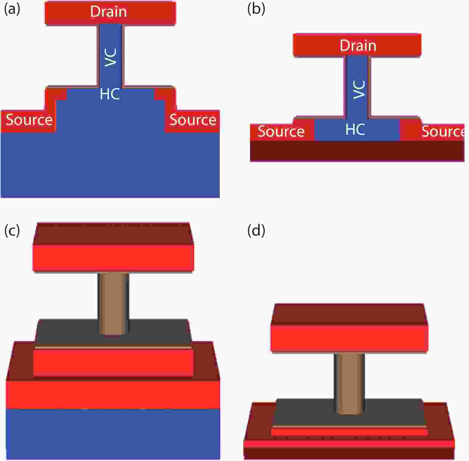
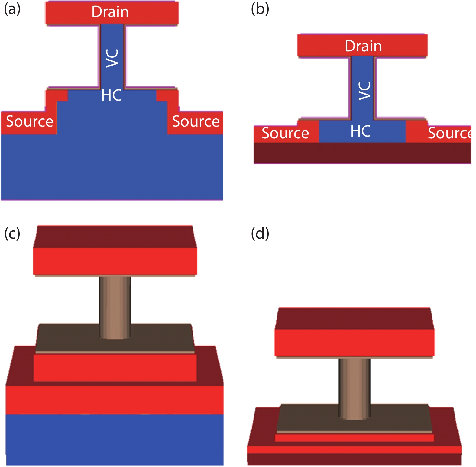
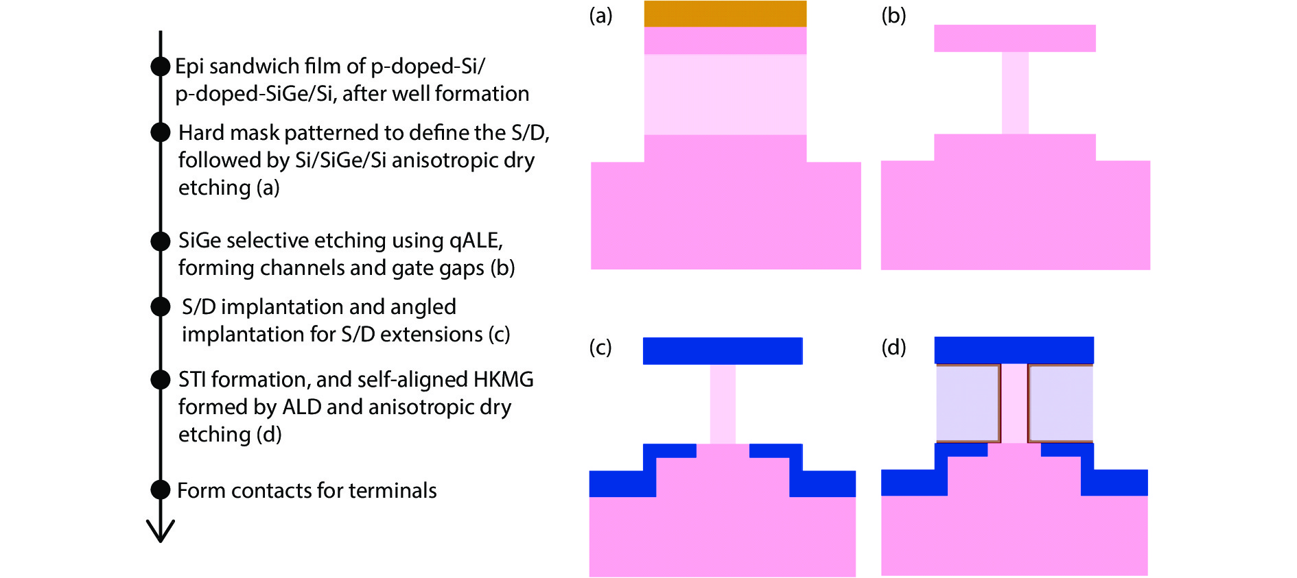
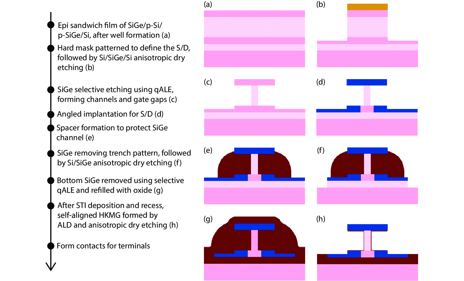
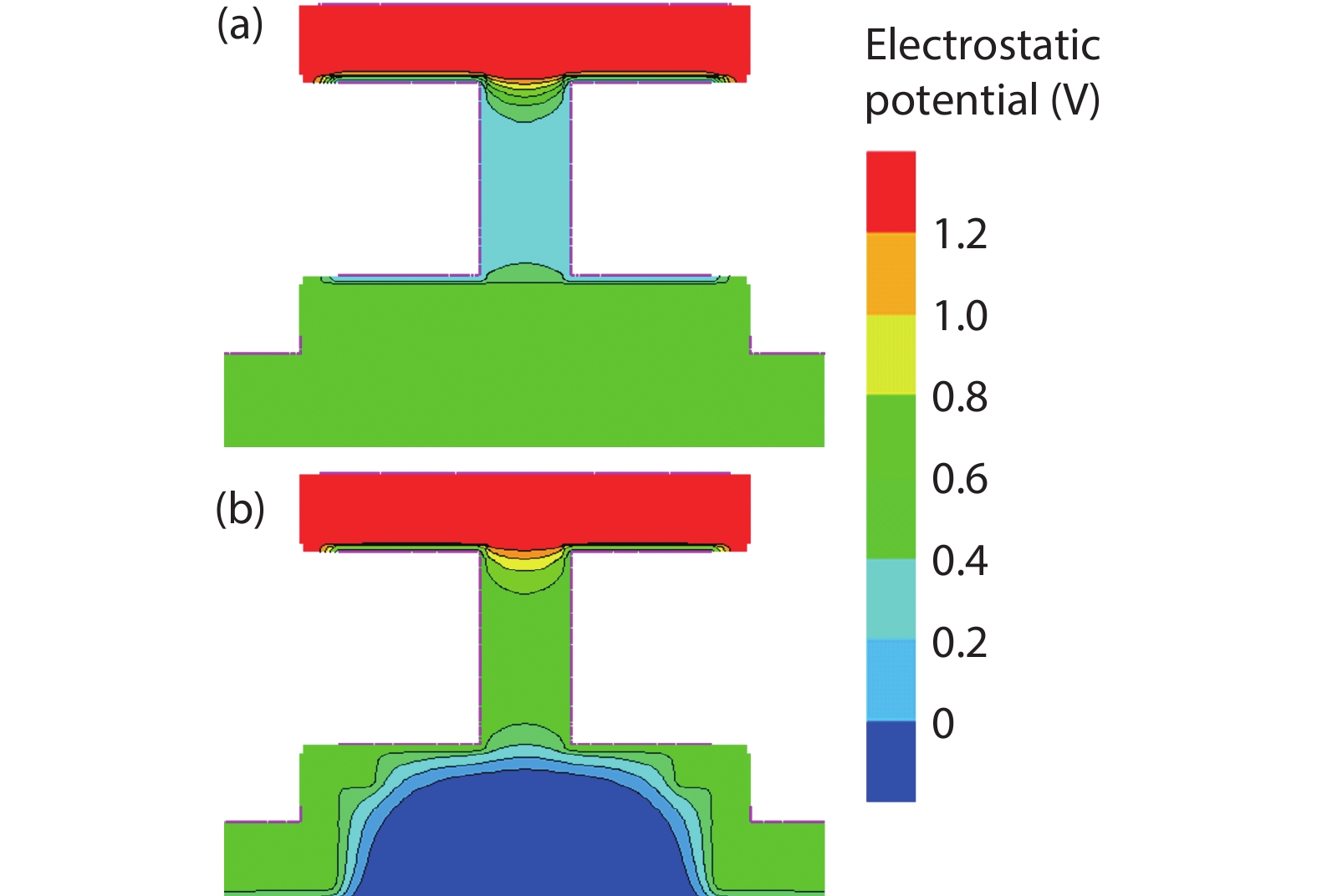
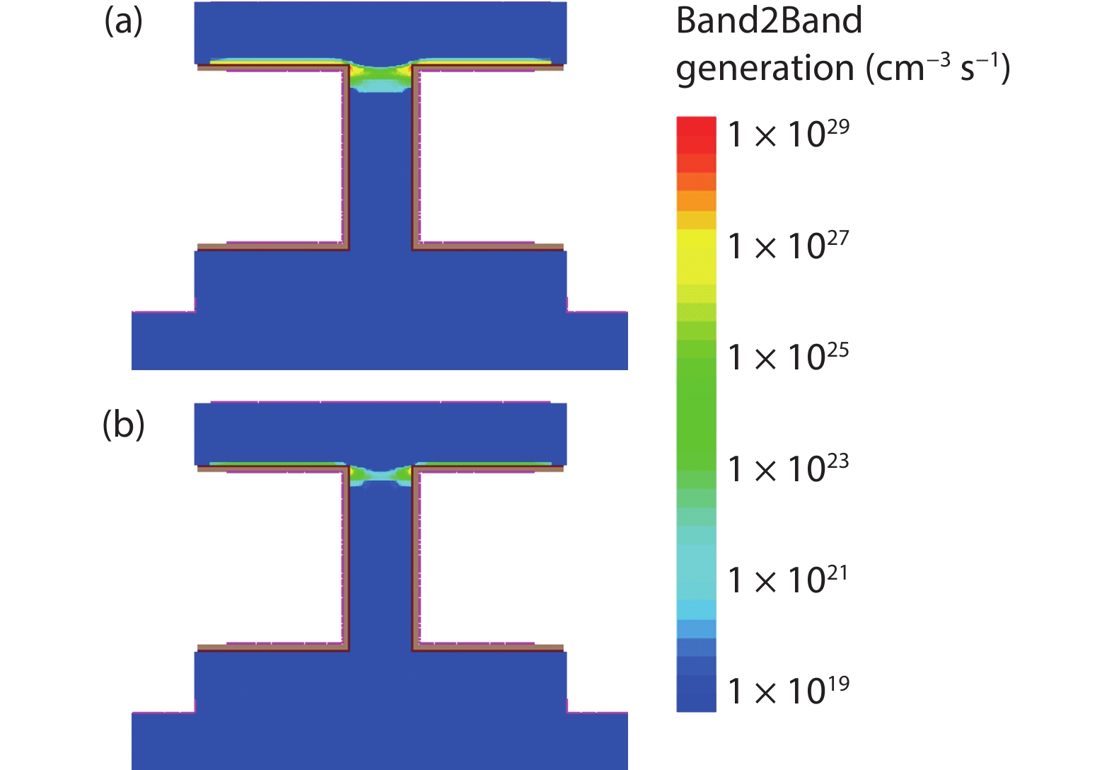
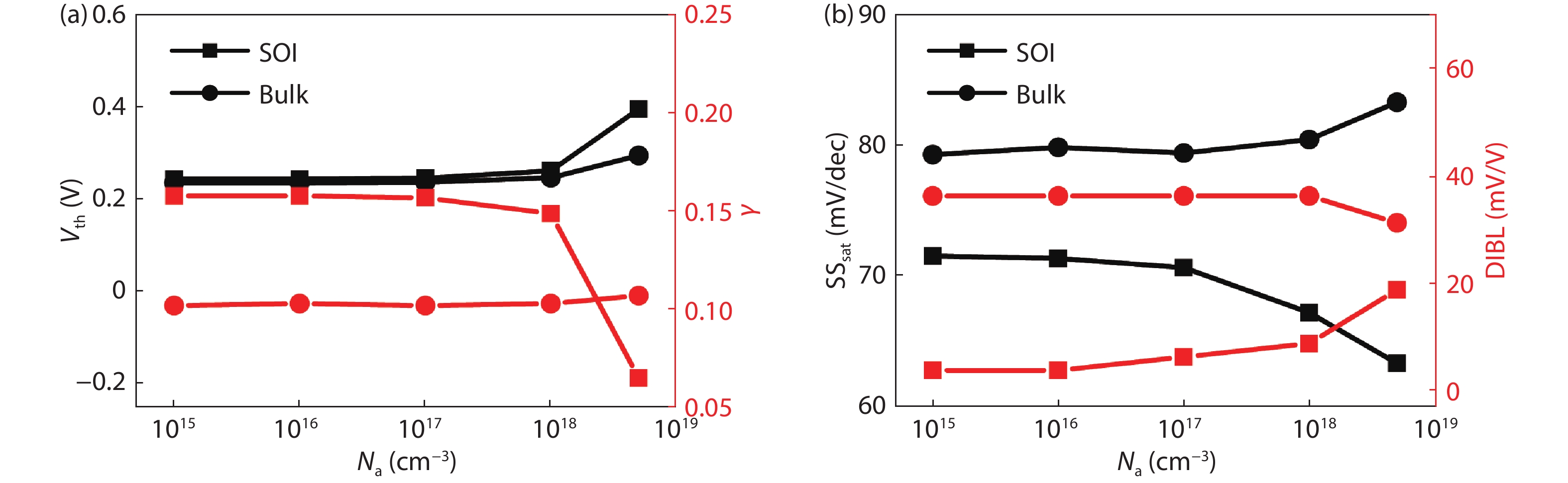
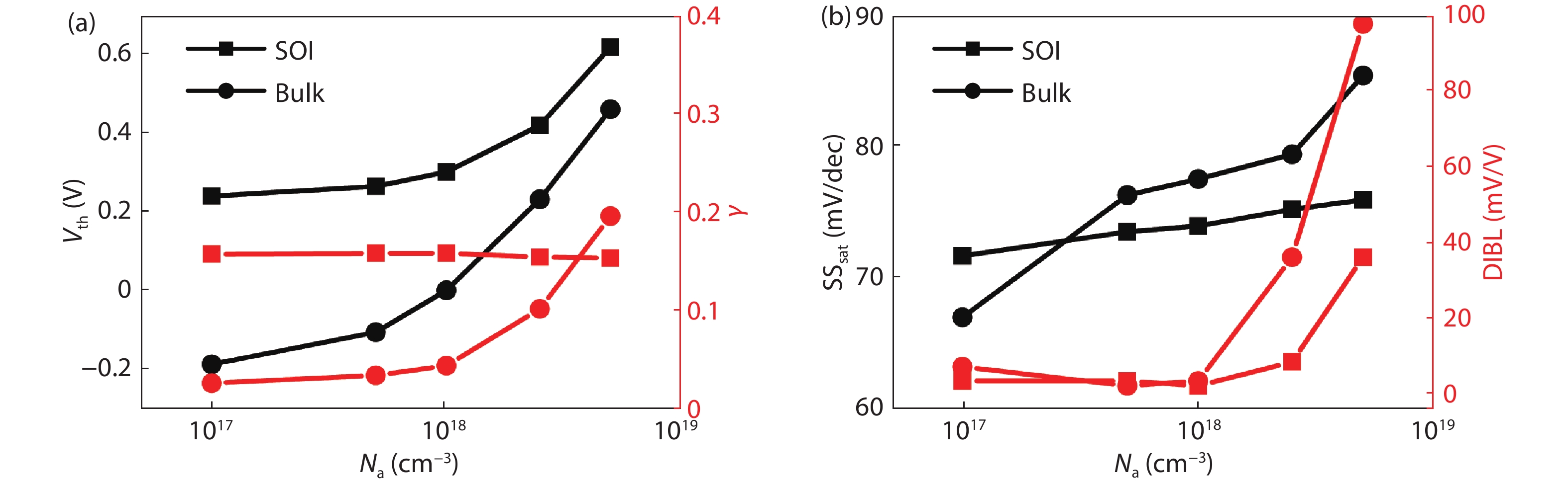
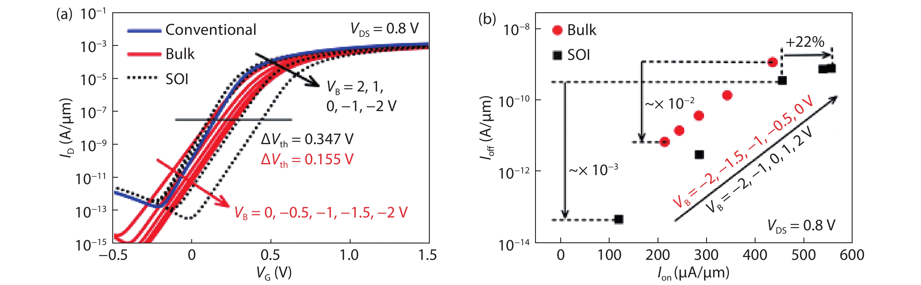
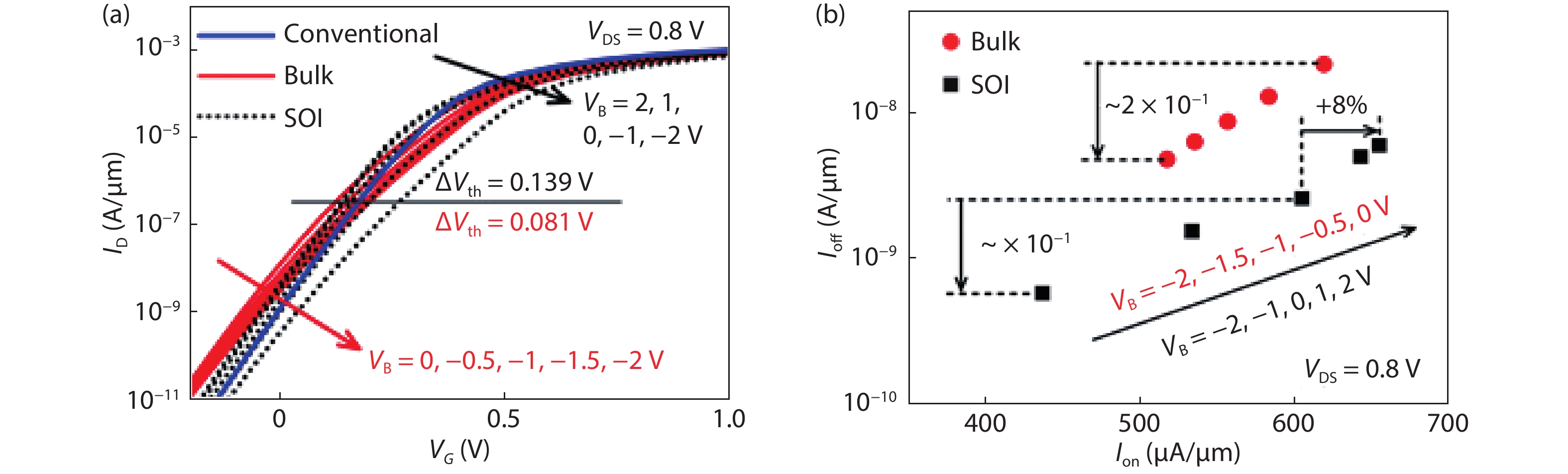
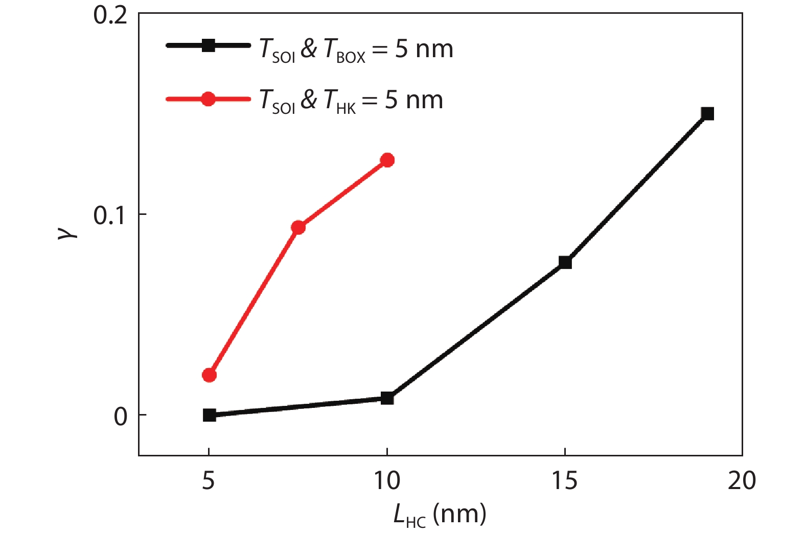
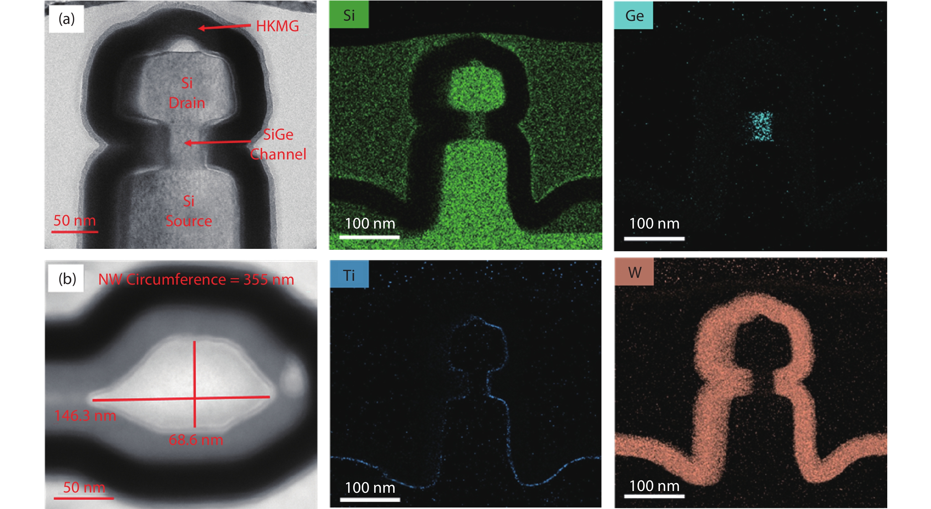
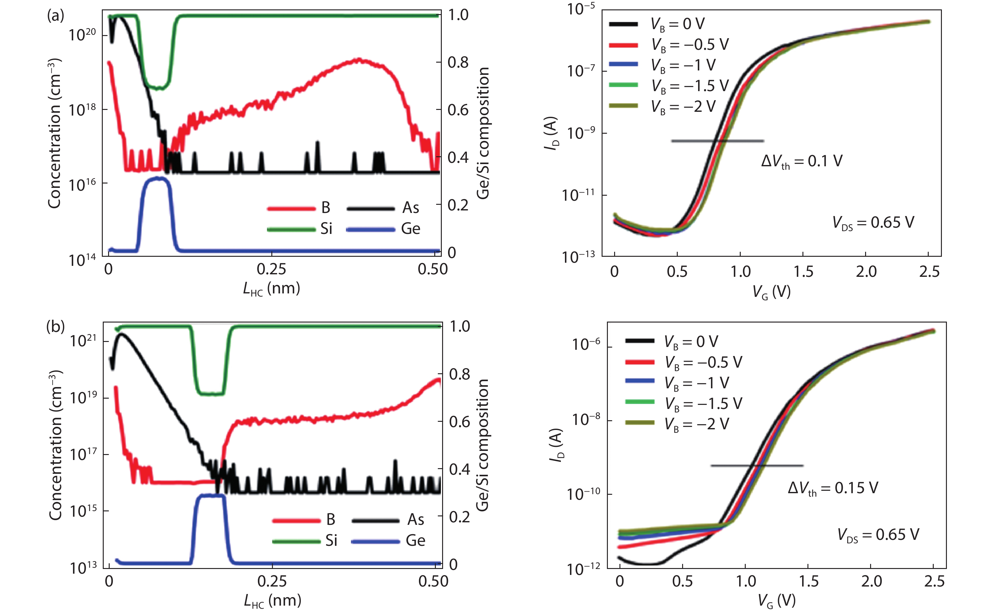
A new type of vertical nanowire (VNW)/nanosheet (VNS) FETs combining a horizontal channel (HC) with bulk/back-gate electrode configuration, including Bulk-HC and FD-SOI-HC VNWFET, is proposed and investigated by TCAD simulation. Comparisons were carried out between conventional VNWFET and the proposed devices. FD-SOI-HC VNWFET exhibits better Ion/Ioff ratio and DIBL than Bulk-HC VNWFET. The impact of channel doping and geometric parameters on the electrical characteristic and body factor (γ) of the devices was investigated. Moreover, threshold voltage modulation by bulk/back-gate bias was implemented and a large γ is achieved for wide range Vth modulation. In addition, results of Ion enhancement and Ioff reduction indicate the proposed devices are promising candidates for performance and power optimization of NW/NS circuits by adopting dynamic threshold voltage management. The results of preliminary experimental data are discussed as well.


J. Semicond.
2022, 43(1): 014102 doi: 10.1088/1674-4926/43/1/014102
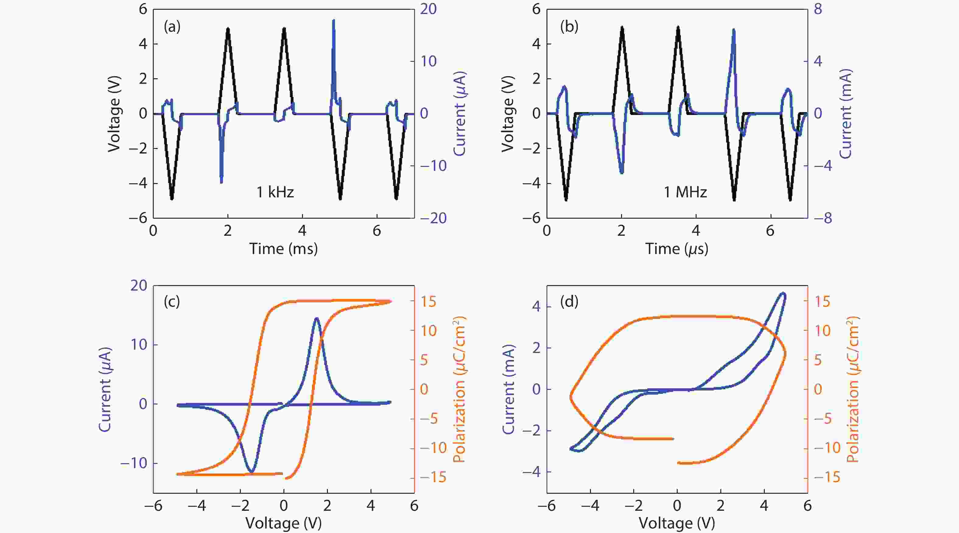
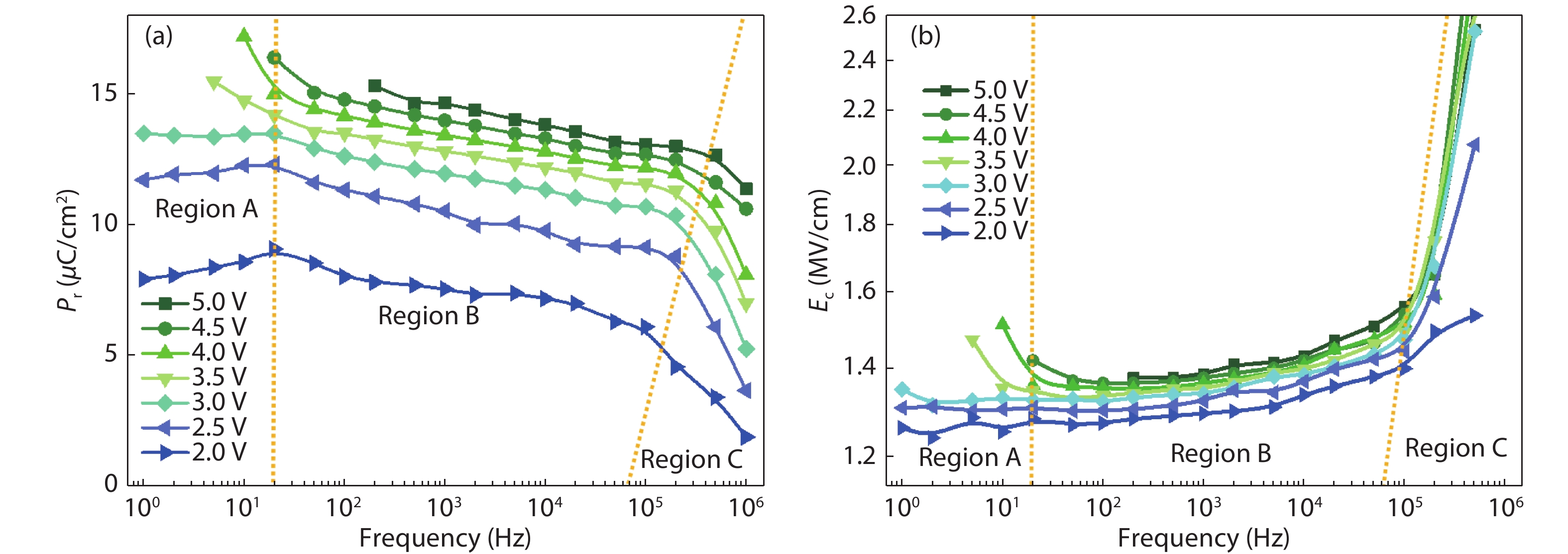
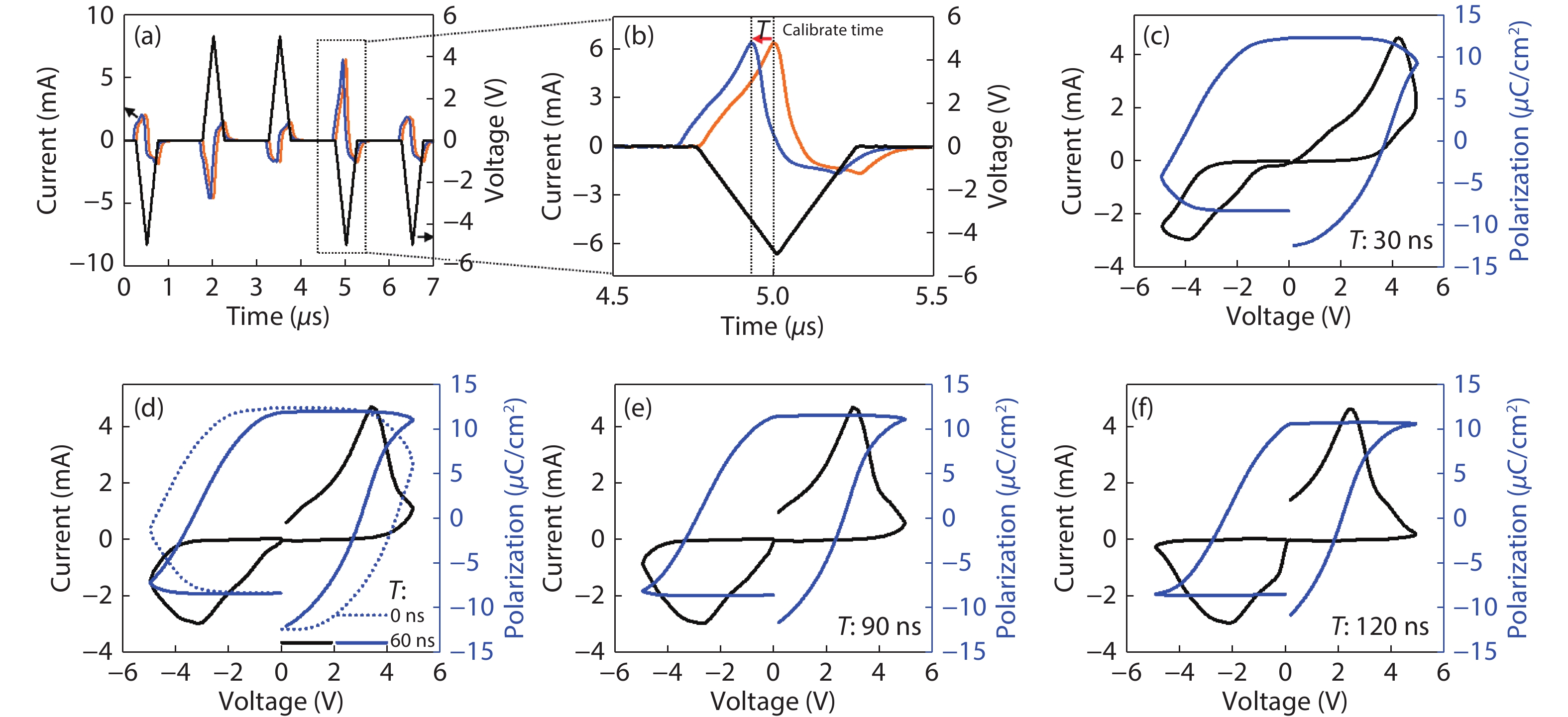
Ferroelectric hysteresis loop measurement under high driving frequency generally faces great challenges. Parasitic factors in testing circuits such as leakage current and RC delay could result in abnormal hysteresis loops with erroneous remnant polarization (Pr) and coercive field (Ec). In this study, positive-up-negative-down (PUND) measurement under a wide frequency range was performed on a 10-nm thick Hf0.5Zr0.5O2 ferroelectric film. Detailed analysis on the leakage current and RC delay was conducted as the polarization switching occurs in the FE capacitor. After considering the time lag caused by RC delay, reasonable calibration of current response over the voltage pulse stimulus was employed in the integral of polarization current over time. In such a method, rational P–V loops measured at high frequencies (>1 MHz) was successfully achieved. This work provides a comprehensive understanding on the effect of parasitic factors on the polarization switching behavior of FE films.