Issue Browser
Volume 42, Issue 8,
Aug 2021


J. Semicond.
2021, 42(8): 081001 doi: 10.1088/1674-4926/42/8/081001
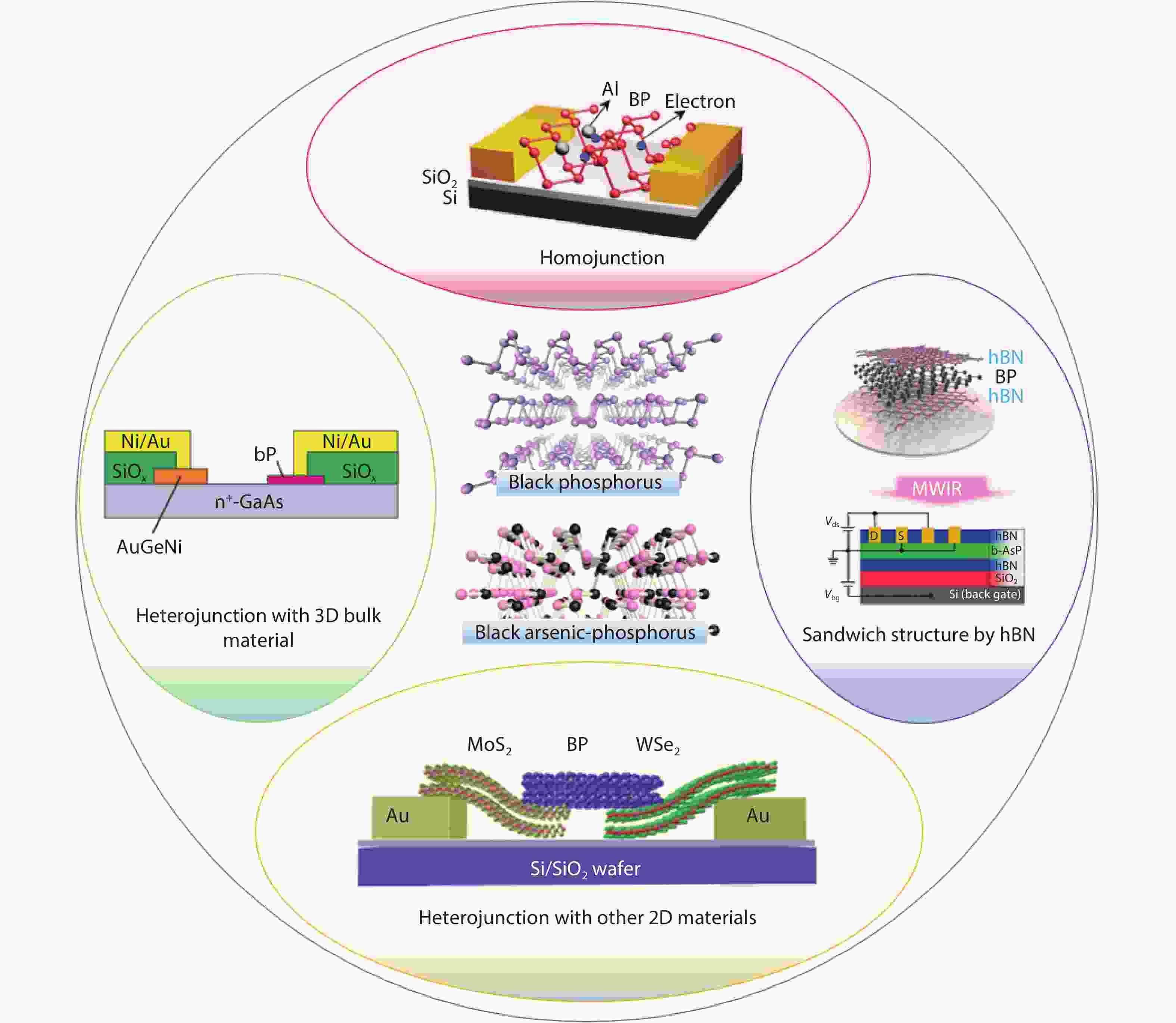
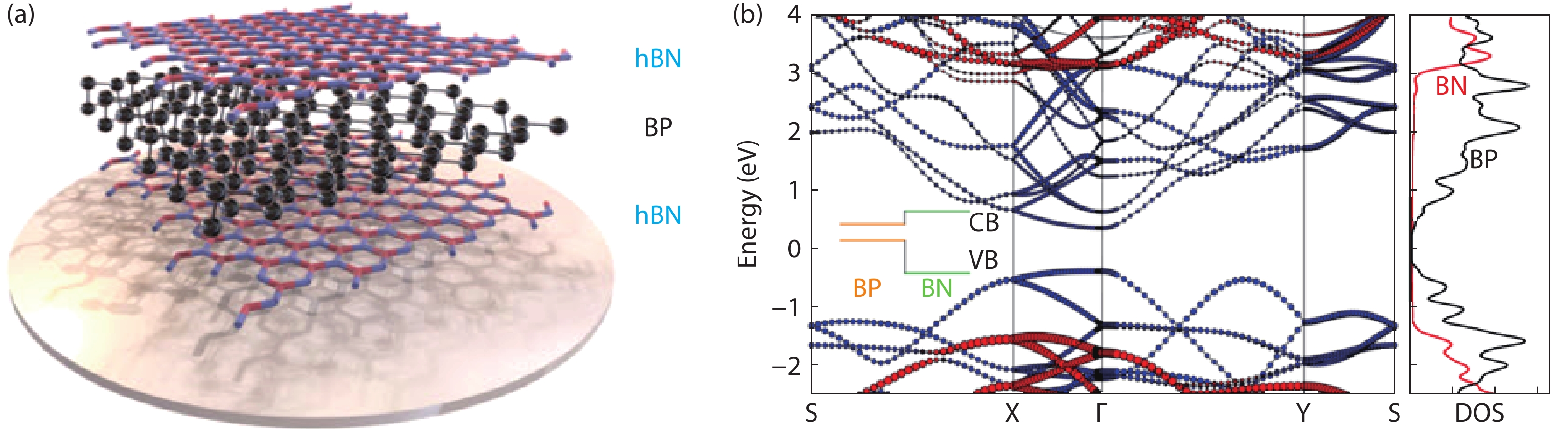
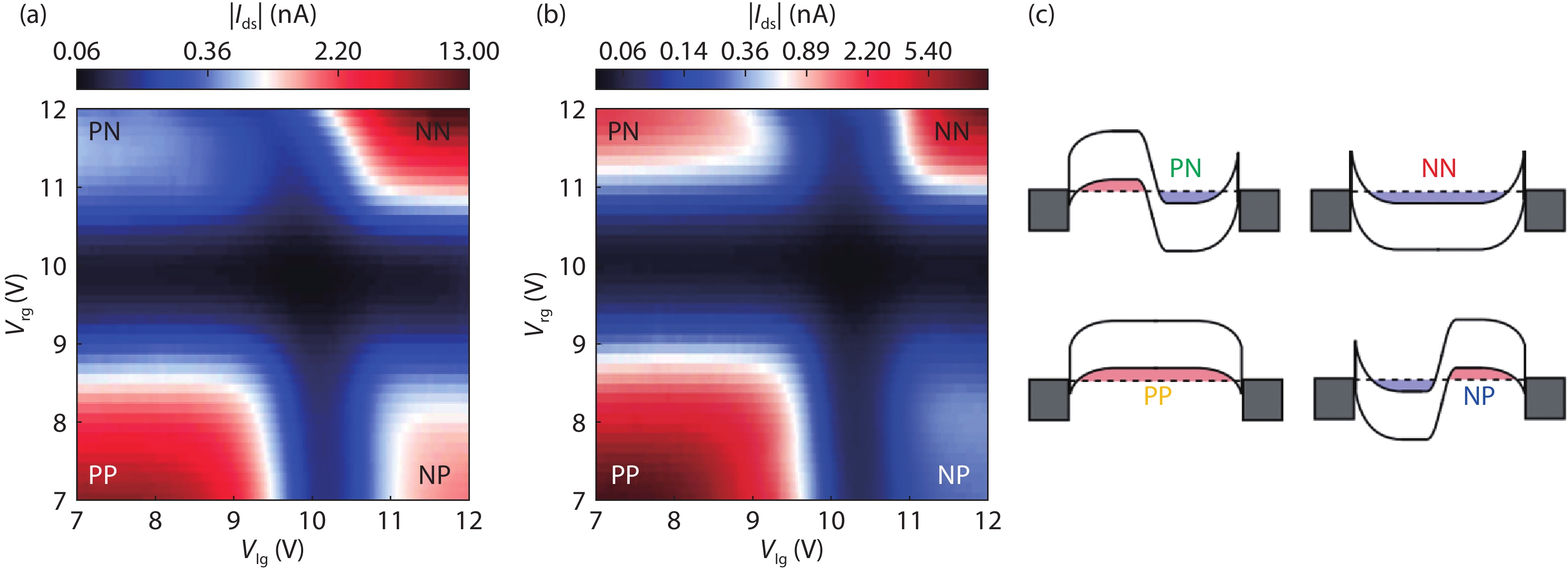
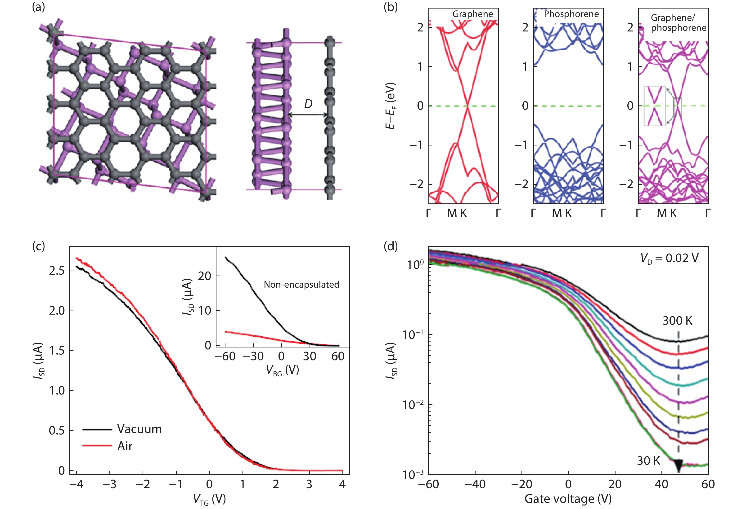
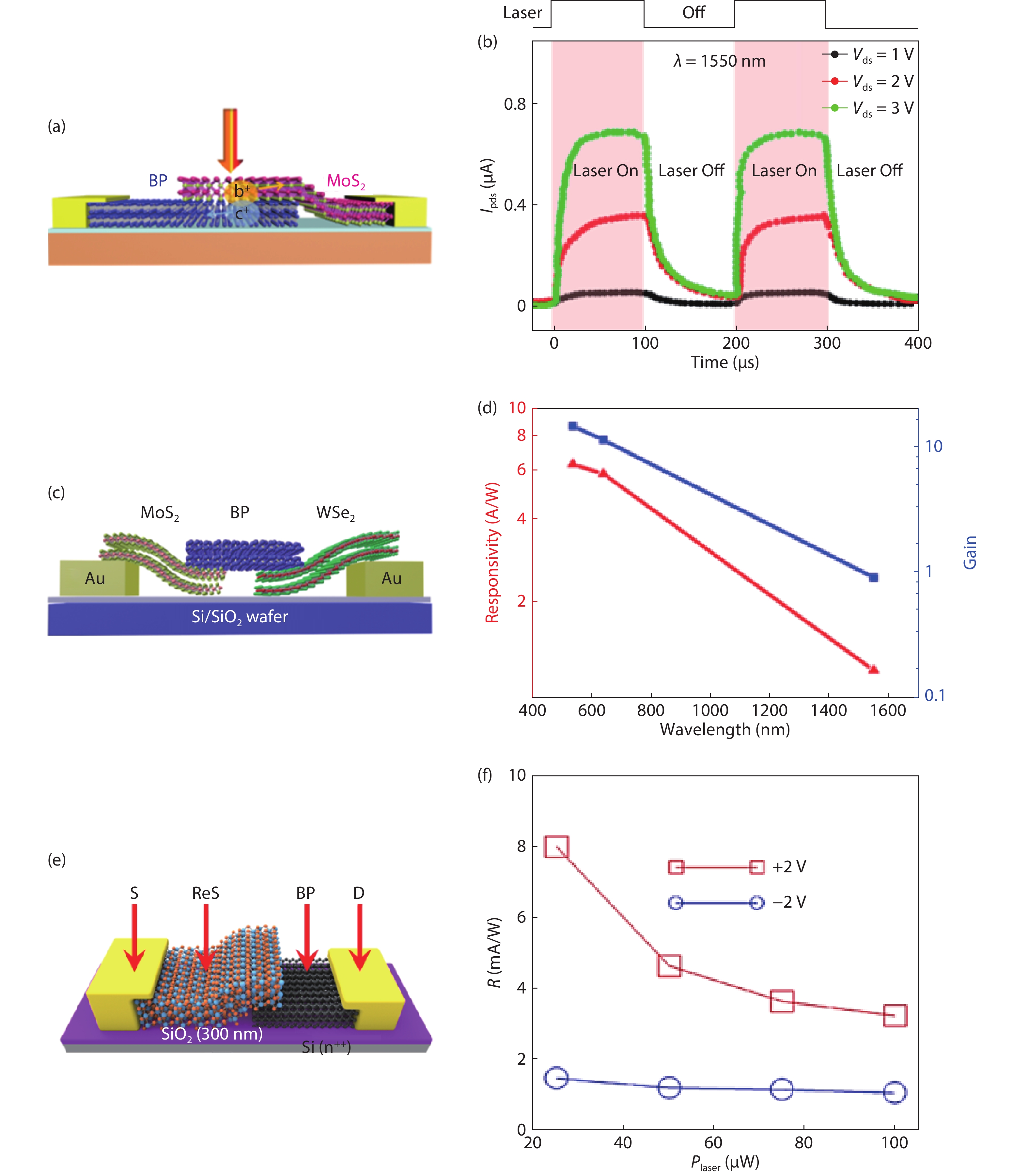
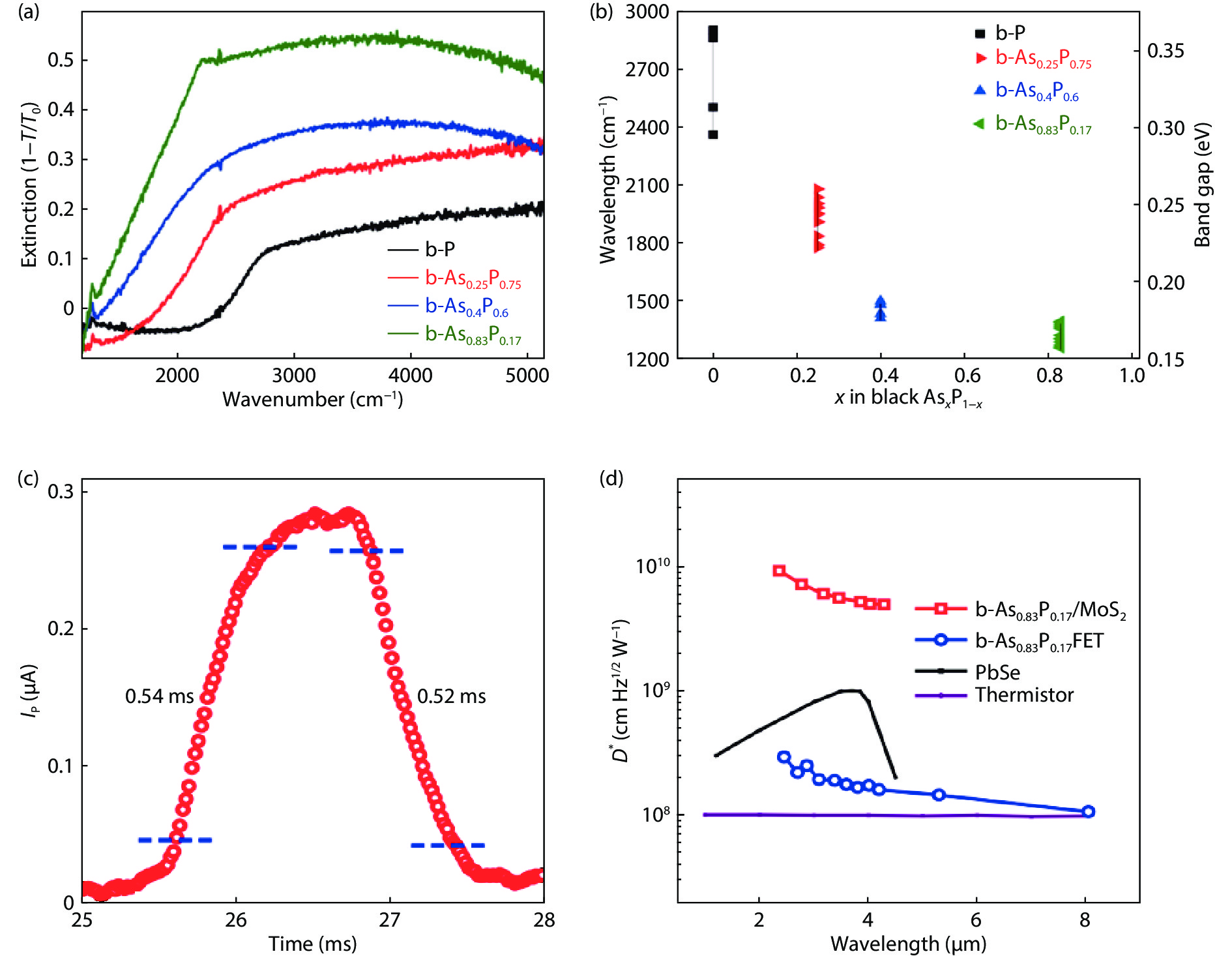
Black phosphorus (BP), an emerging two-dimensional material, is considered a promising candidate for next-generation electronic and optoelectronic devices due to in-plane anisotropy, high mobility, and direct bandgap. However, BP devices face challenges due to their limited stability, photo-response speed, and detection range. To enhance BP with powerful electrical and optical performance, the BP heterostructures can be created. In this review, the state-of-the-art heterostructures and their electrical and optoelectronic applications based on black phosphorus are discussed. Five parts introduce the performance of BP-based devices, including black phosphorus sandwich structure by hBN with better stability and higher mobility, black phosphorus homojunction by dual-gate structure for optical applications, black phosphorus heterojunction with other 2D materials for faster photo-detection, black phosphorus heterojunction integration with 3D bulk material, and BP via As-doping tunable bandgap enabling photo-detection up to 8.2 μm. Finally, we discuss the challenges and prospects for BP electrical and optical devices and applications.


J. Semicond.
2021, 42(8): 081801 doi: 10.1088/1674-4926/42/8/081801
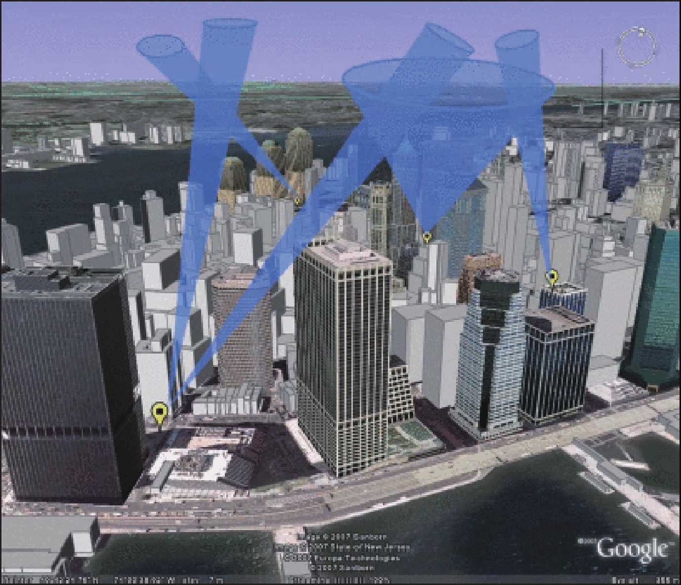
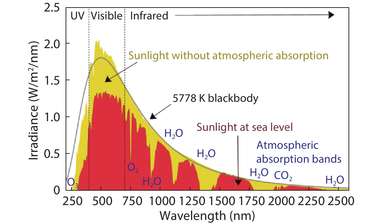
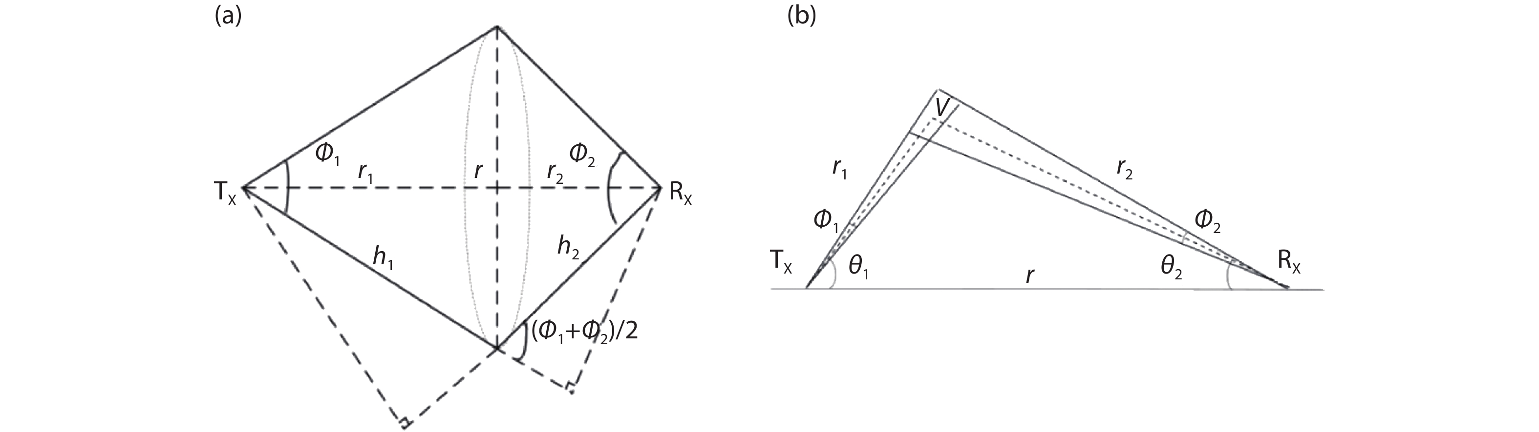
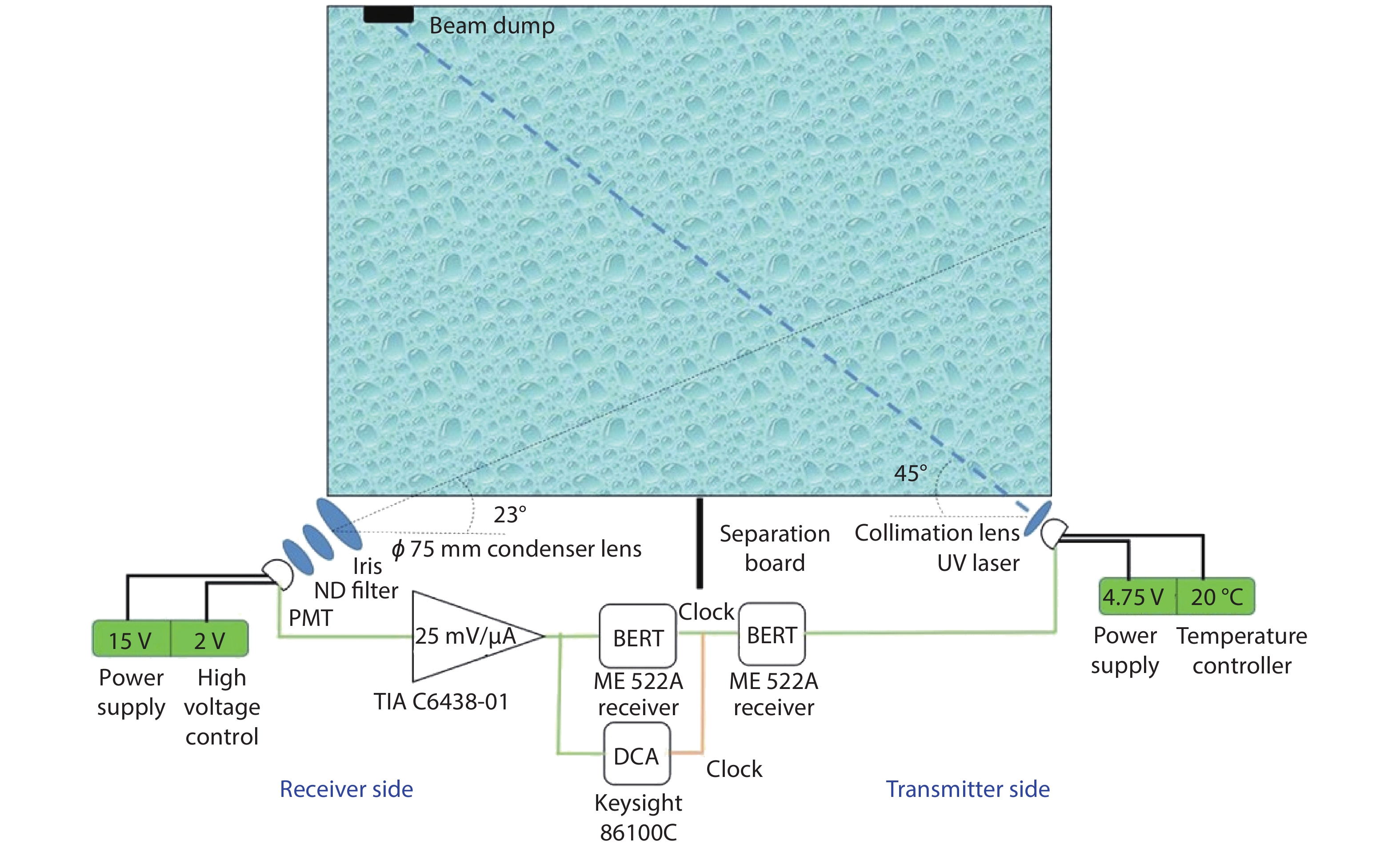
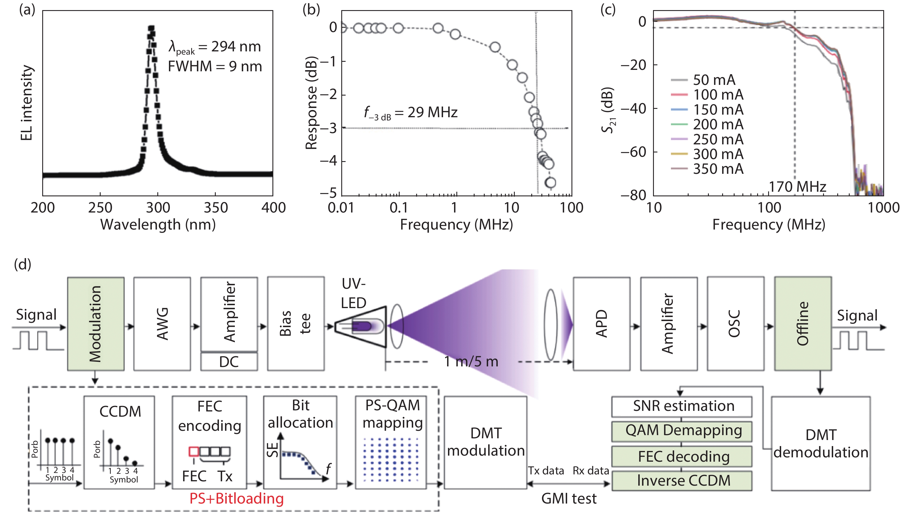
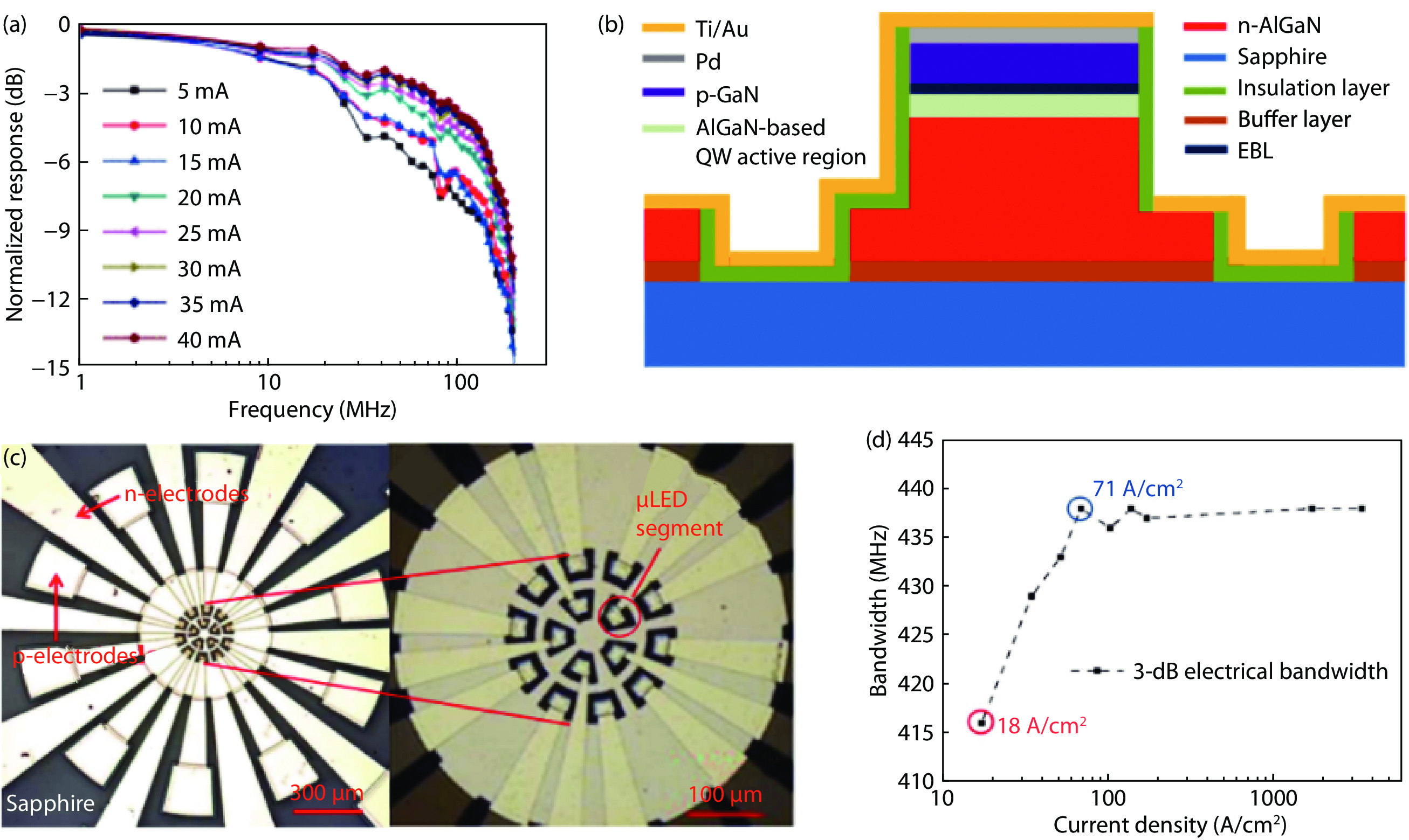
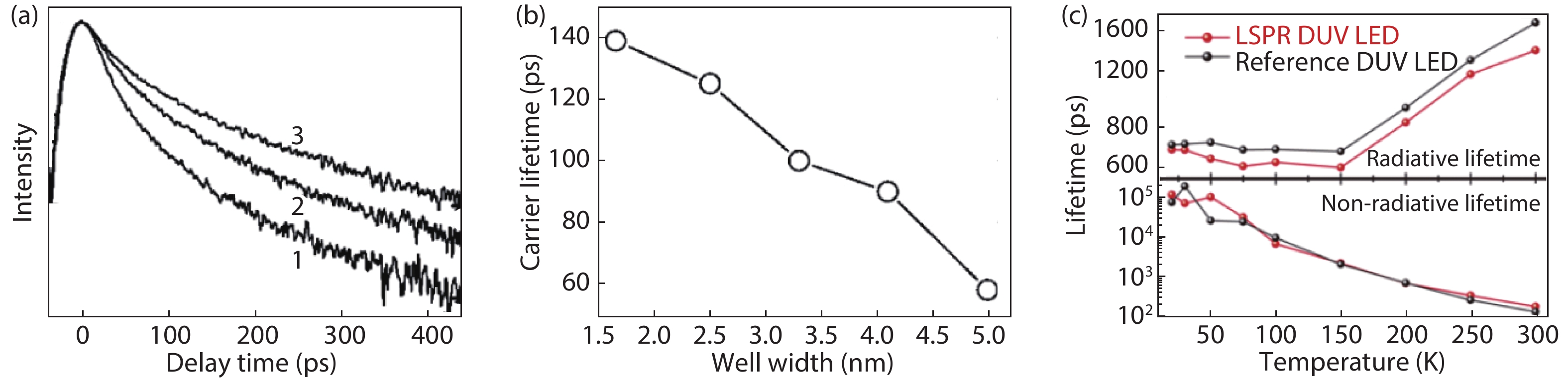
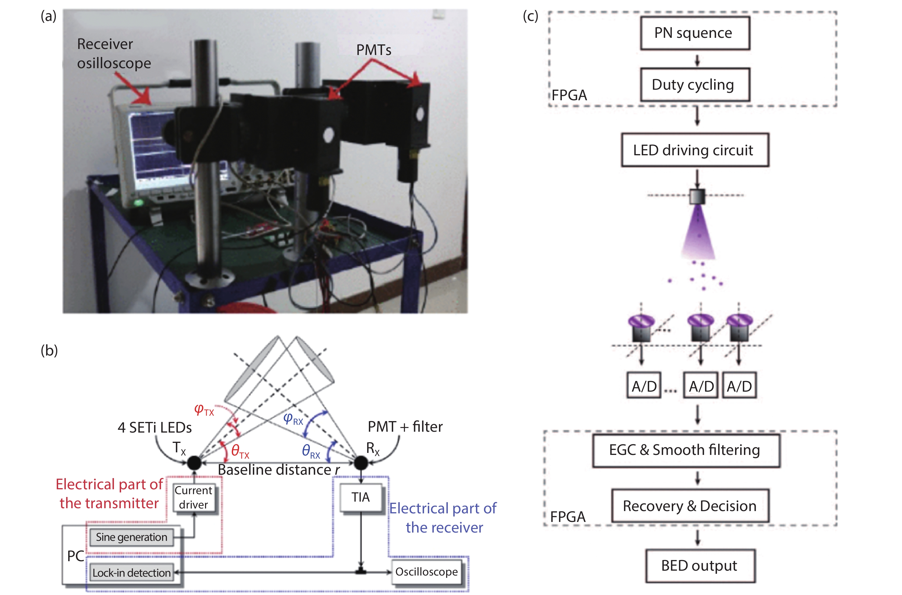
With recent developments of deep ultraviolet (DUV) light-emitting diodes and solar-blind detectors, UV communication (UVC) shows great potential in replacing traditional wireless communication in more and more scenarios. Based on the atmospheric scattering of UV radiation, UVC has gained considerable attention due to its non-line-of-sight ability, omnidirectional communication links and low background noise. These advantages make UVC an ideal option for covert secure communication, especially for military communication. In this review, we present the history and working principle of UVC with a special focus on its light sources and detectors. Comprehensive comparison and application of its light sources and detectors are provided to the best of our knowledge. We further discuss the future application and outlook of UVC. Hopefully, this review will offer valuable insights into the future development of UVC.


J. Semicond.
2021, 42(8): 082001 doi: 10.1088/1674-4926/42/8/082001
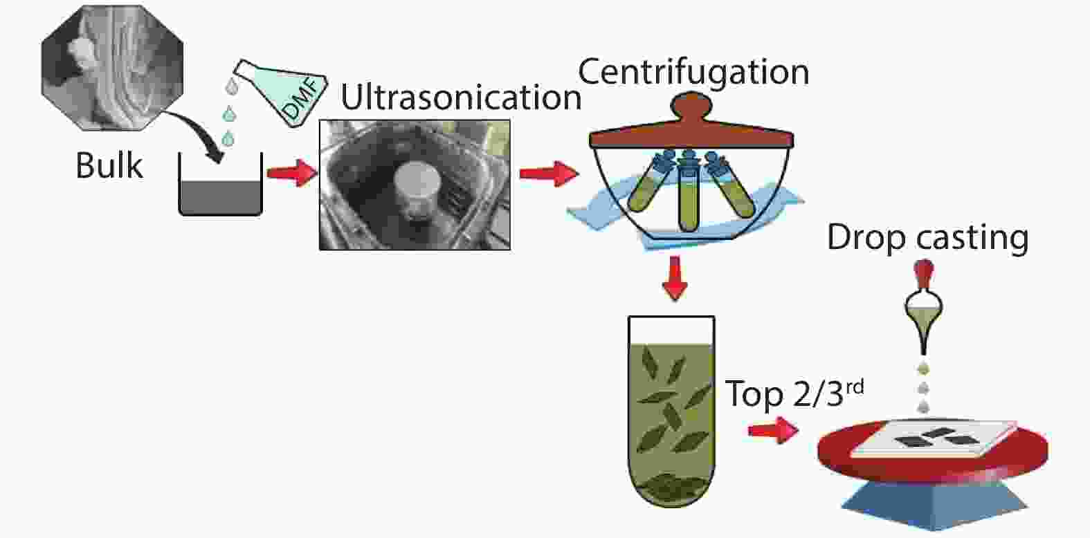
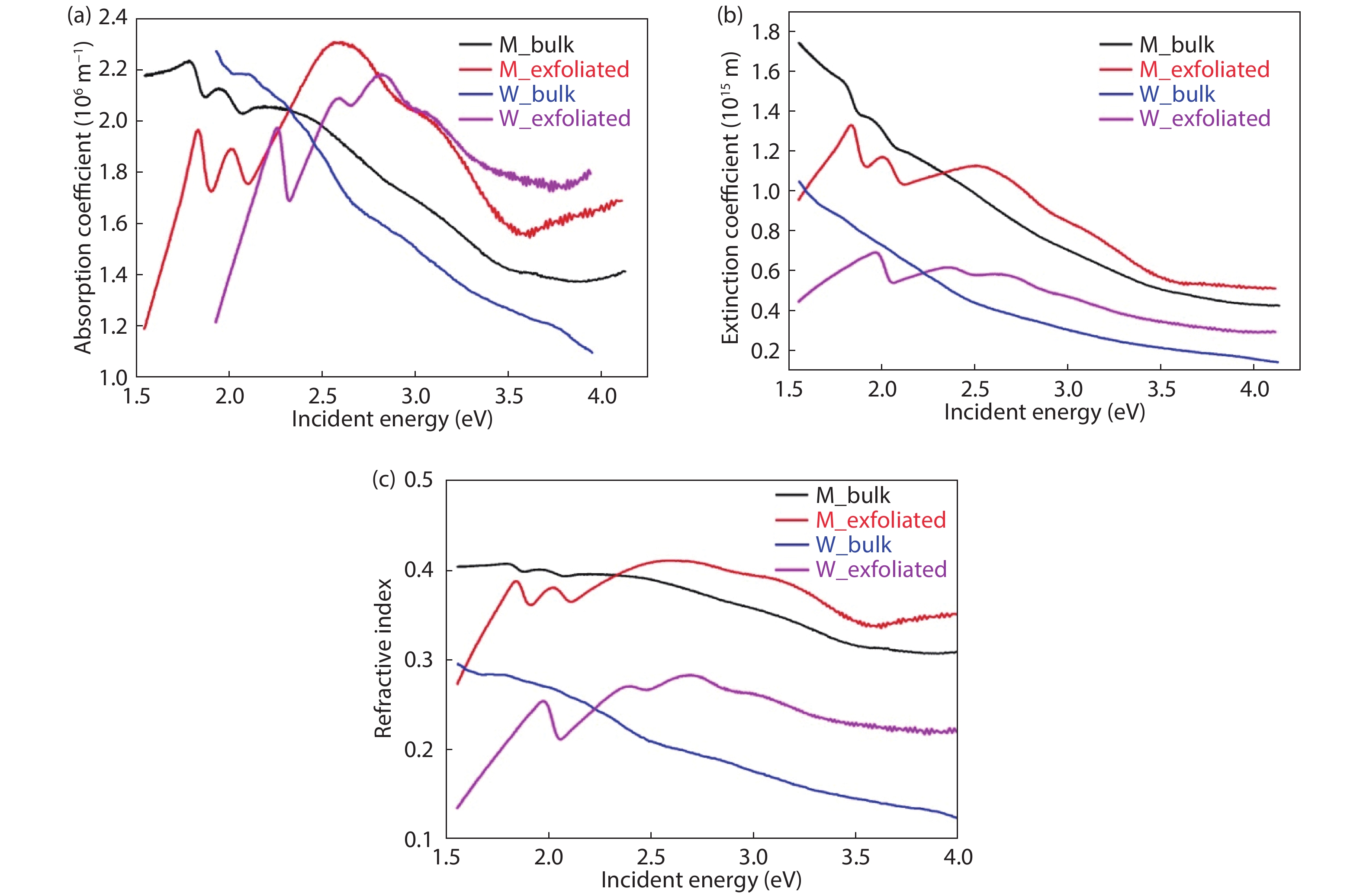
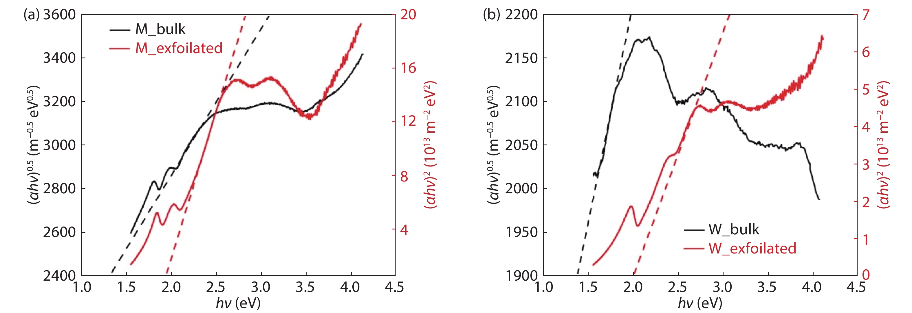
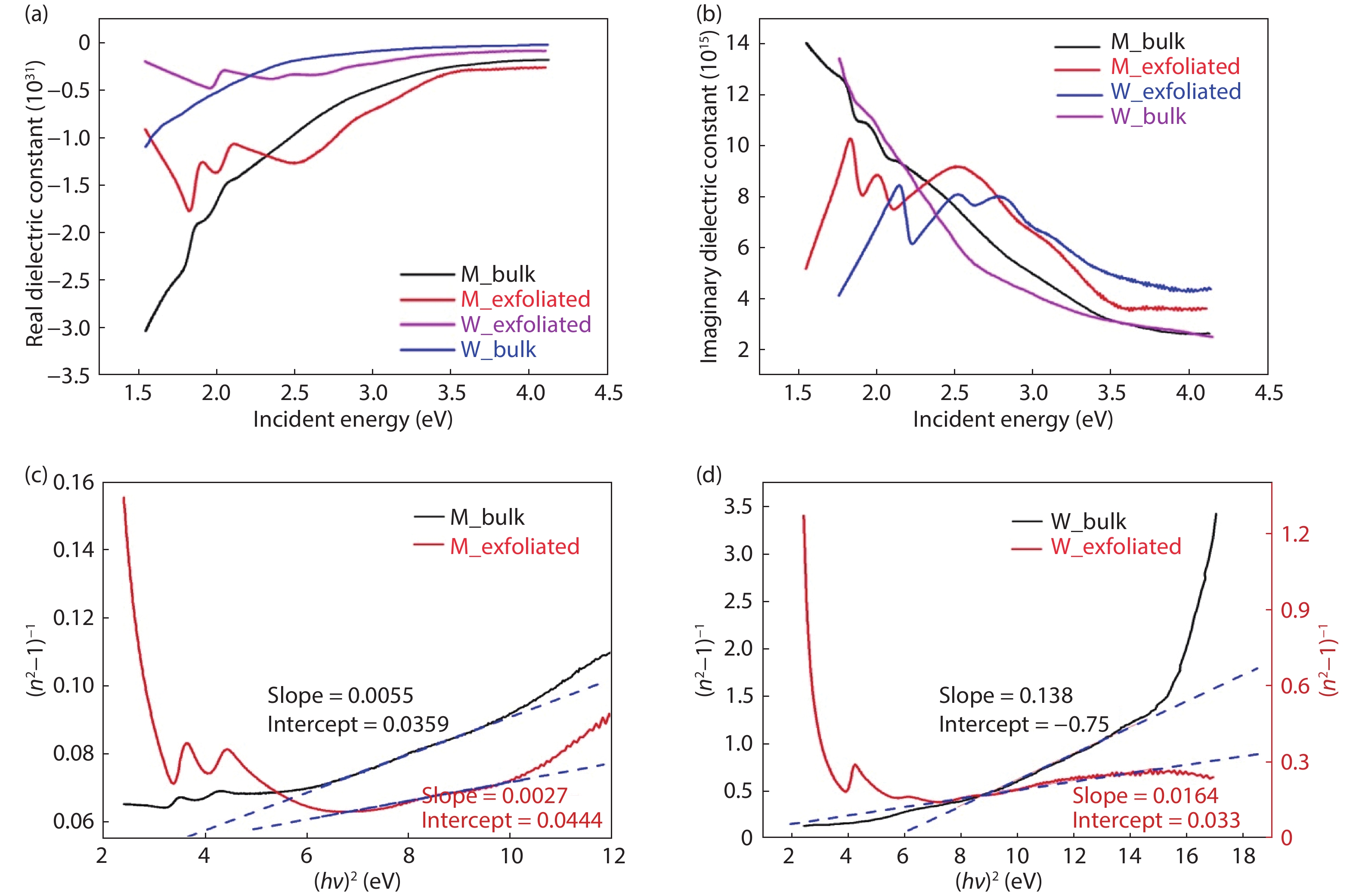
A remarkable refinement in the optical behavior of two-dimensional transition metal dichalcogenides (TMDs) has been brought to light when cleaved from their respective bulks. These atomically thin direct bandgap semiconductors are highly responsive to optical energy which proposes the route for futuristic photonic devices. In this manuscript, we have substantially focused on the optical study of MoS2 and WS2 nanosheets and comparative analysis with their bulk counterparts. The synthesis of nanosheets has been accomplished with liquid exfoliation followed by fabrication of thin films with drop-casting technique. X-ray diffraction and field emission scanning electron microscopy affirmed the morphology, whereas, UV–visible spectroscopy served as the primary tool for optical analysis. It was observed that several parameters, like optical conductivity, optical band-gap energy etc. have enhanced statistics in the case of exfoliated nanosheets as compared to their respective bulks. Some researchers have touched upon this analysis for MoS2, but it is completely novel for WS2. We expect our work to clearly distinguish between the optical behaviors of nanoscale and bulk TMDs so as to intensify and strengthen the research related to 2D-layered materials for optoelectronic and photovoltaic applications.


J. Semicond.
2021, 42(8): 082301 doi: 10.1088/1674-4926/42/8/082301

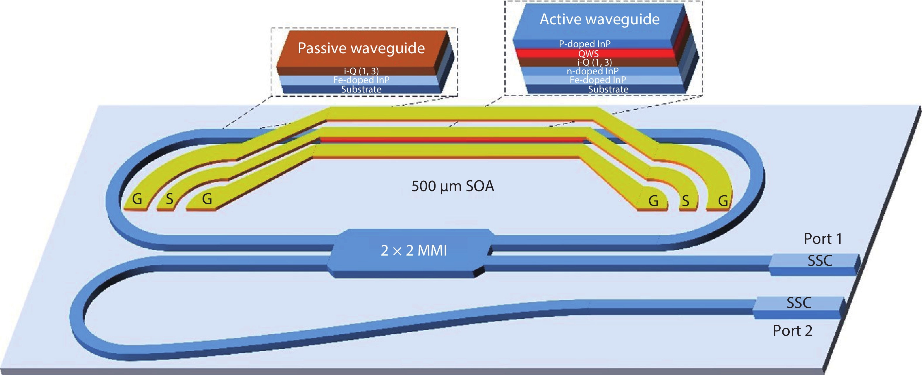
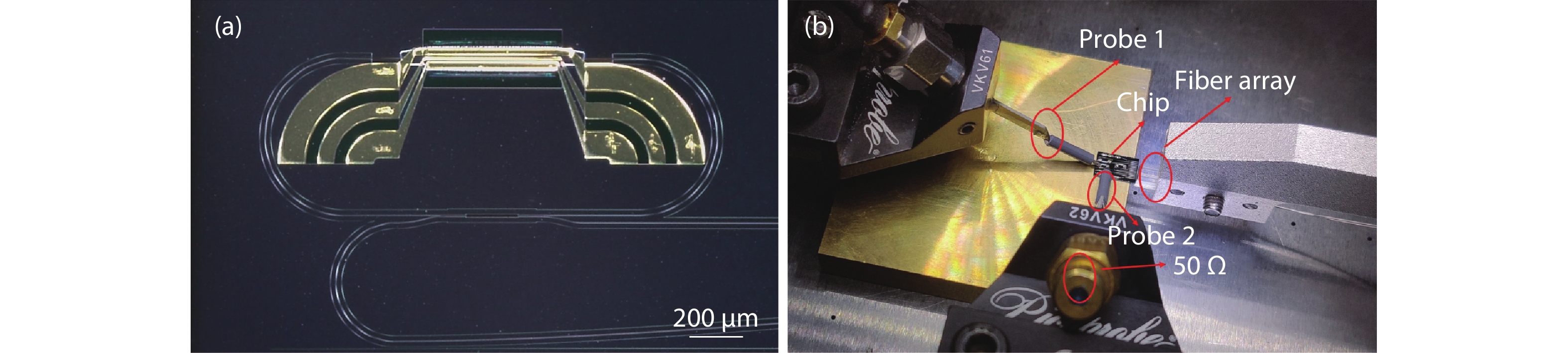
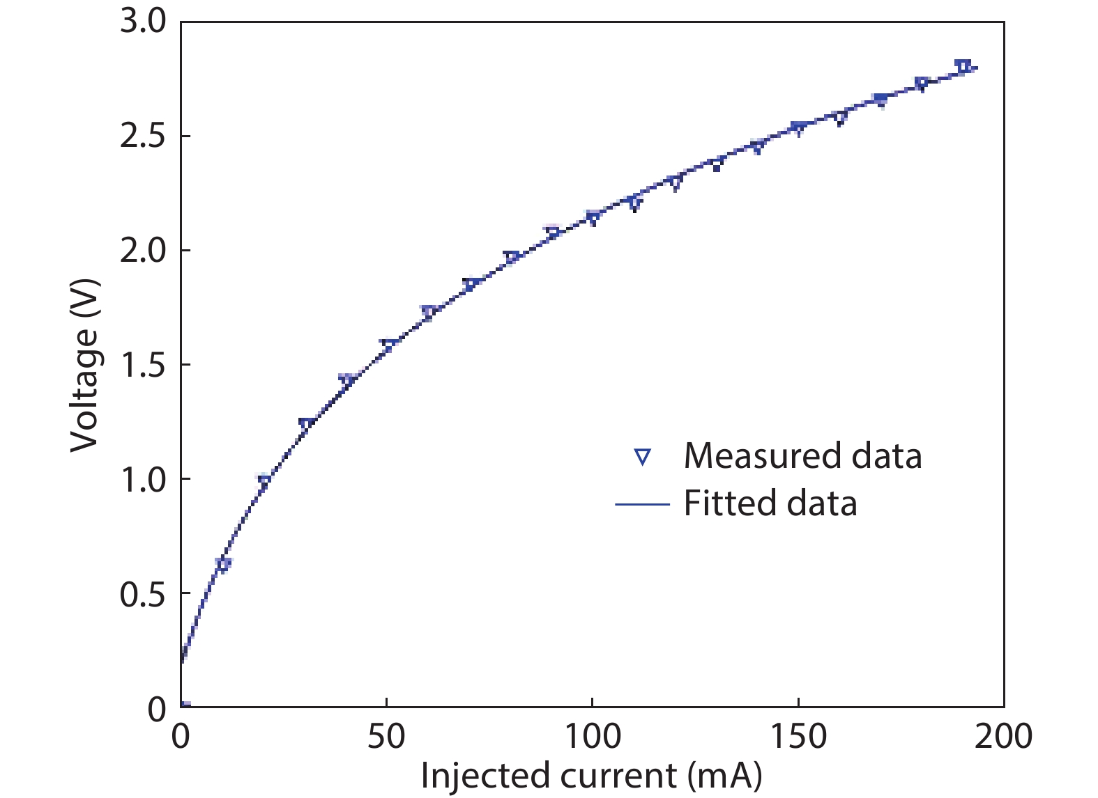
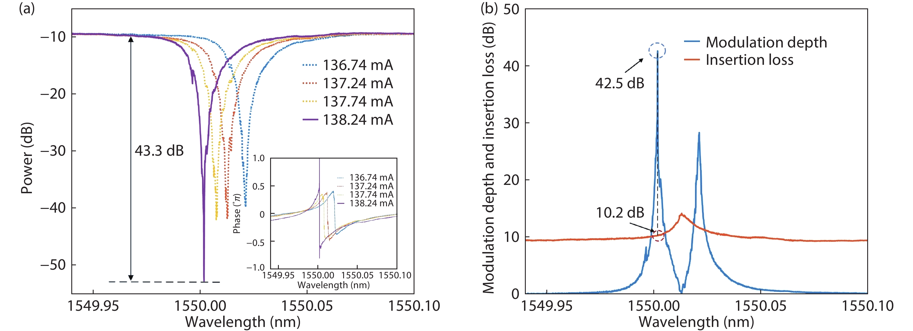
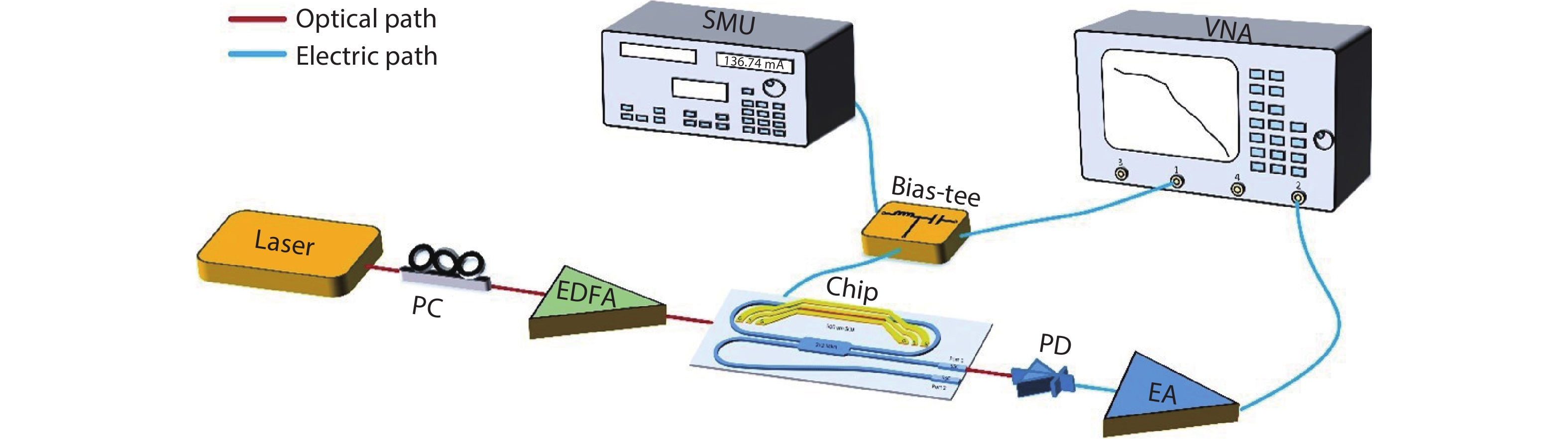
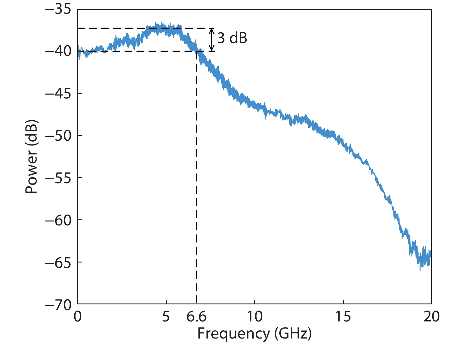
A modulator is an essential building block in the integrated photonics, connecting the electrical with optical signals. The microring modulator gains much attention because of the small footprint, low drive voltage and high extinction ratio. An ultra-low Vpp and high-modulation-depth indium phosphide-based racetrack microring modulator is demonstrated in this paper. The proposed device mainly comprises one racetrack microring, incorporating a semiconductor amplifier, and coupling with a bus waveguide through a multimode interference coupler. Traveling wave electrodes are employed to supply bidirectional bias ports, terminating with a 50-Ω impedance. The on/off extinction ratio of the microring reaches 43.3 dB due to the delicately tuning of the gain. An 11 mV Vpp, a maximum 42.5 dB modulation depth and a 6.6 GHz bandwidth are realized, respectively. This proposed microring modulator could enrich the functionalities and designability of the fundamental integrated devices.

J. Semicond.
2021, 42(8): 082401 doi: 10.1088/1674-4926/42/8/082401

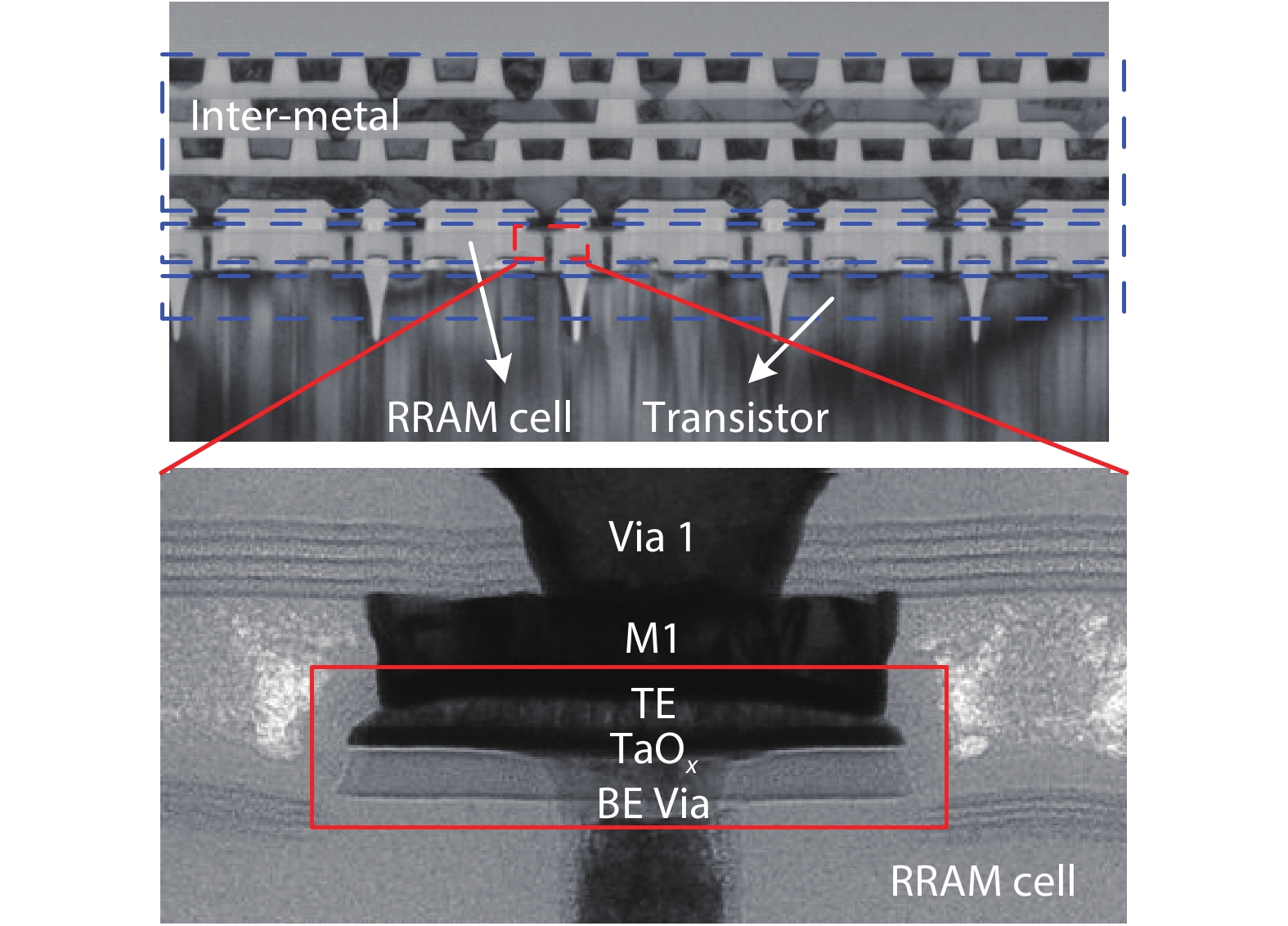
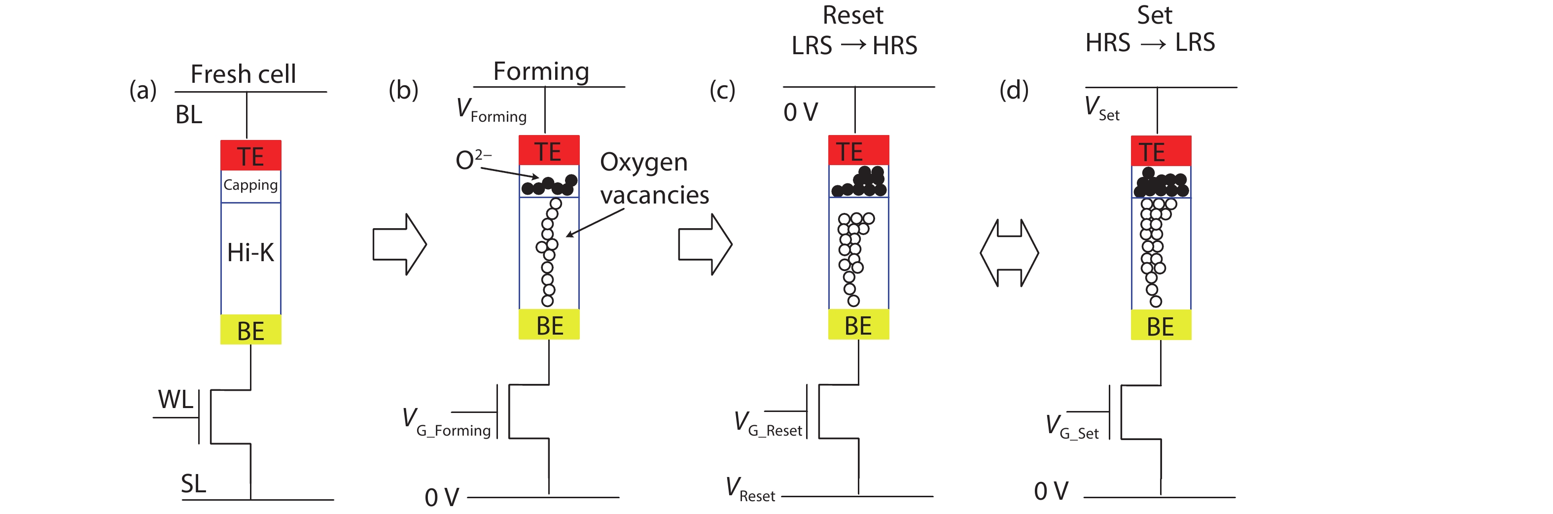
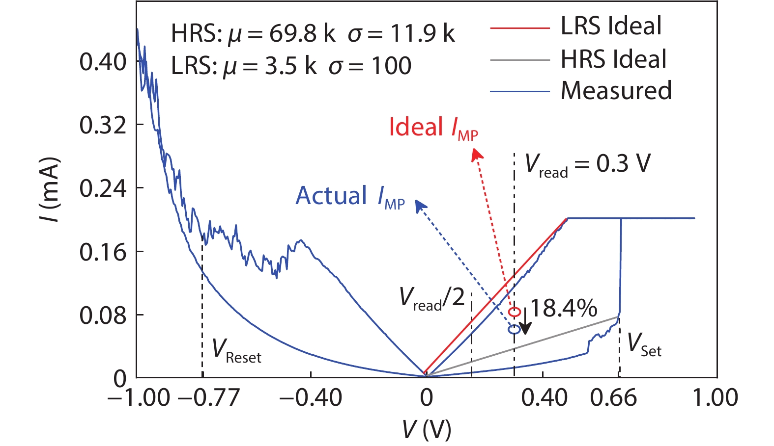
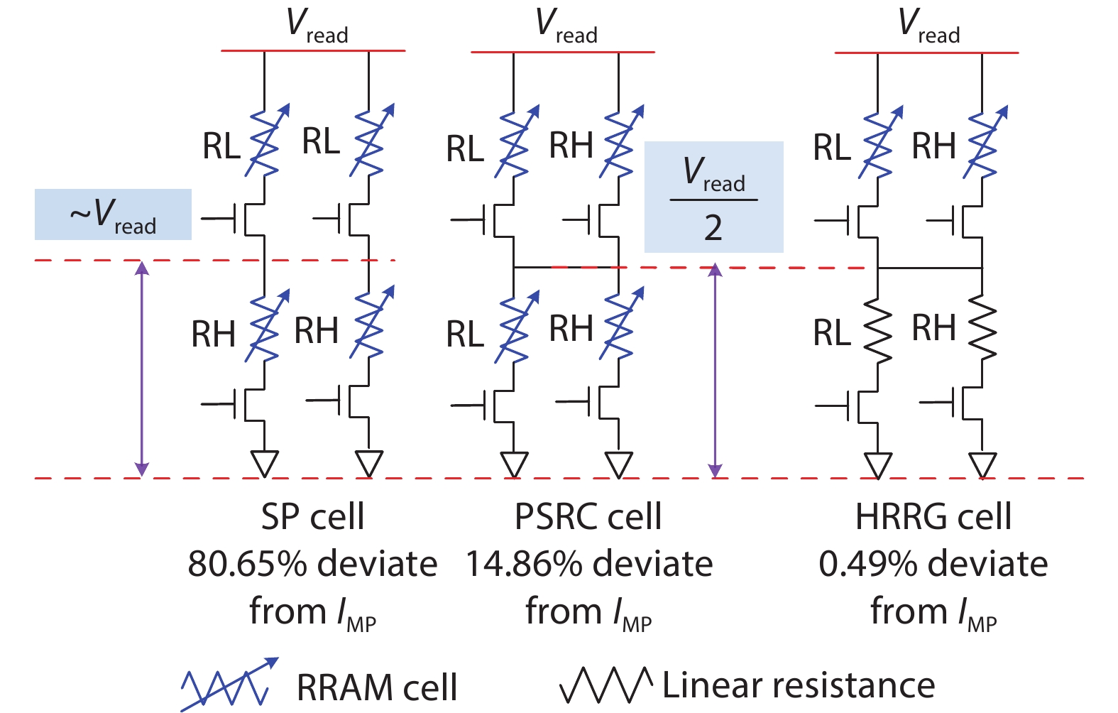
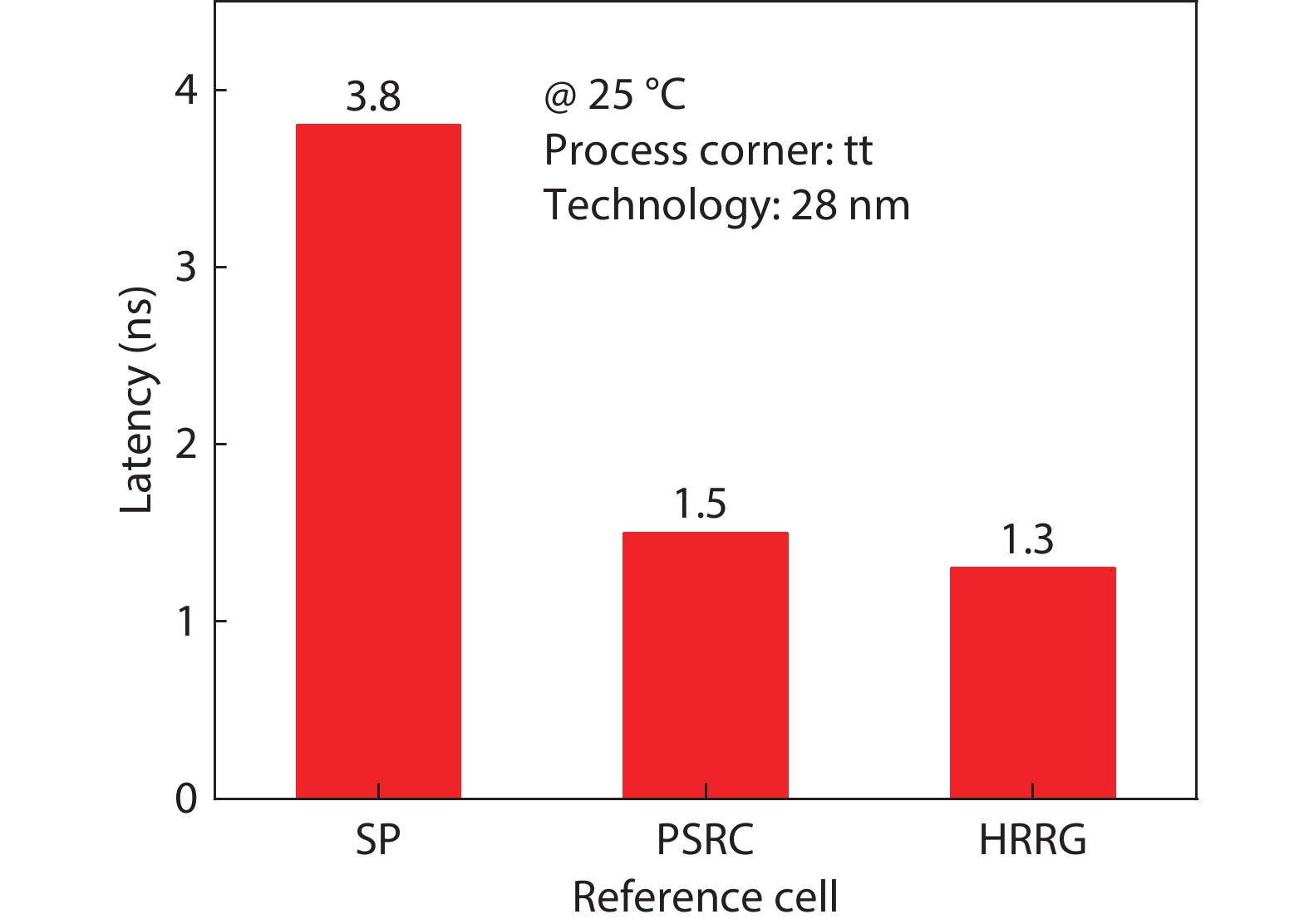
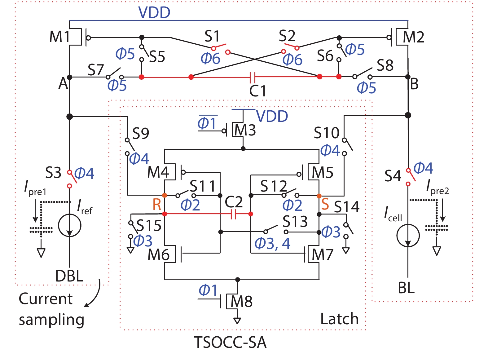
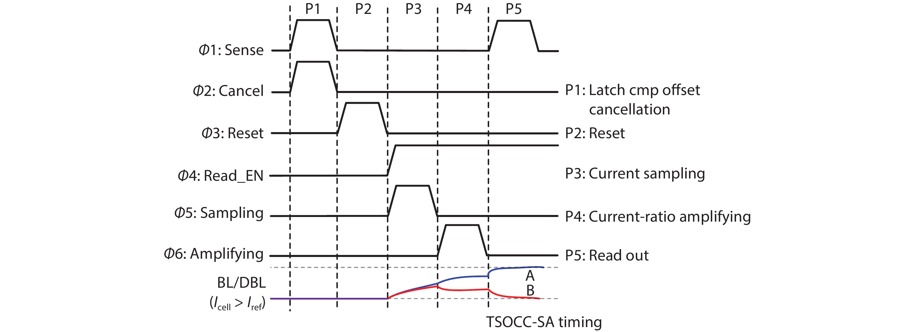
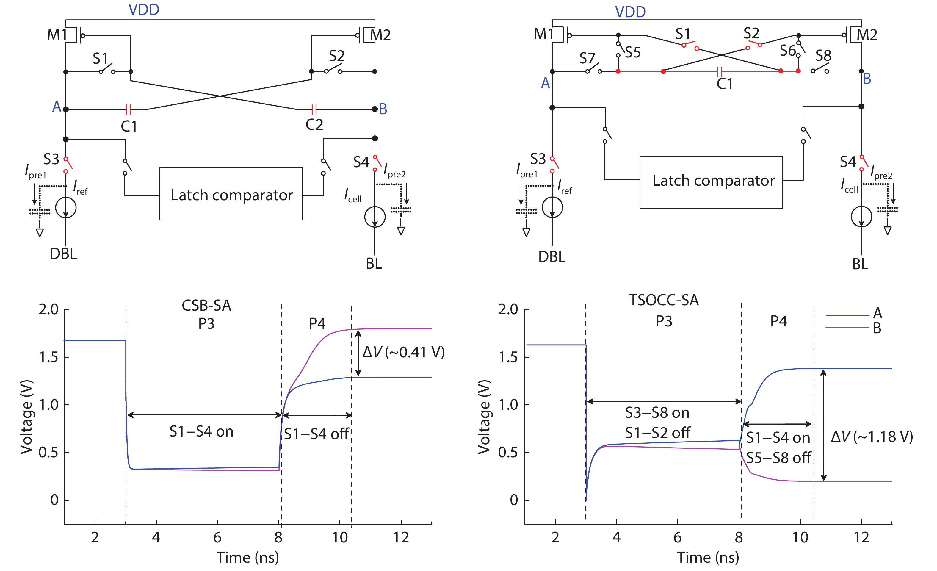
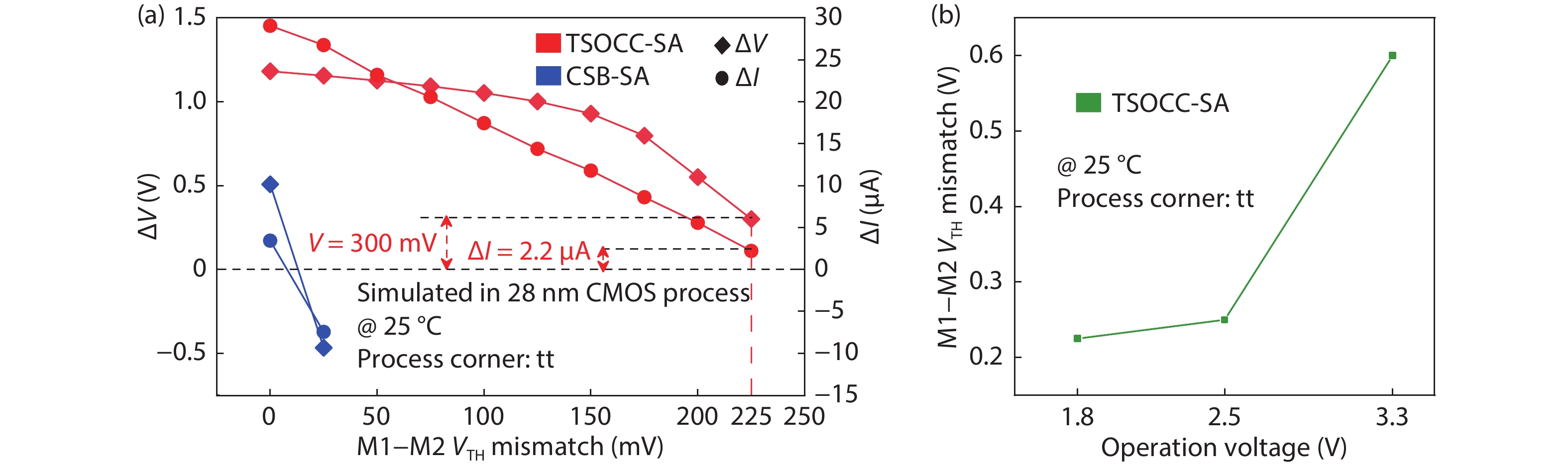
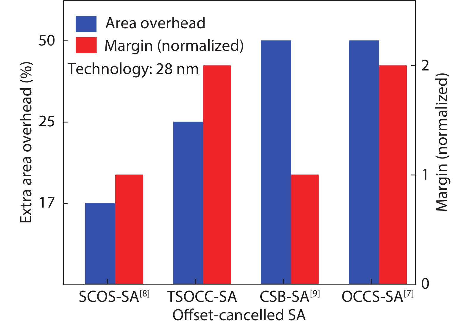
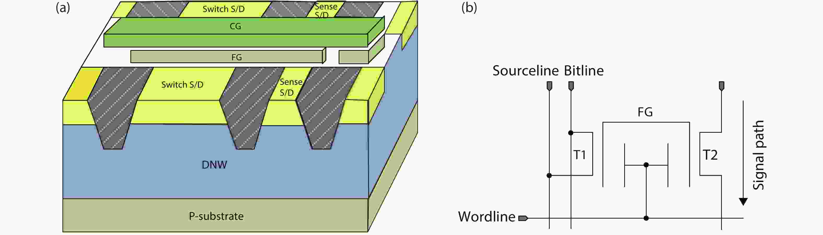
In this work, two process-variation-tolerant schemes for a current-mode sense amplifier (CSA) of RRAM were proposed: (1) hybrid read reference generator (HRRG) that tracks process-voltage-temperature (PVT) variations and solve the nonlinear issue of the RRAM cells; (2) a two-stage offset-cancelled current sense amplifier (TSOCC-SA) with only two capacitors achieves a double sensing margin and a high tolerance of device mismatch. The simulation results in 28 nm CMOS technology show that the HRRG can provide a read reference that tracks PVT variations and solves the nonlinear issue of the RRAM cells. The proposed TSOCC-SA can tolerate over 64% device mismatch.

J. Semicond.
2021, 42(8): 082801 doi: 10.1088/1674-4926/42/8/082801
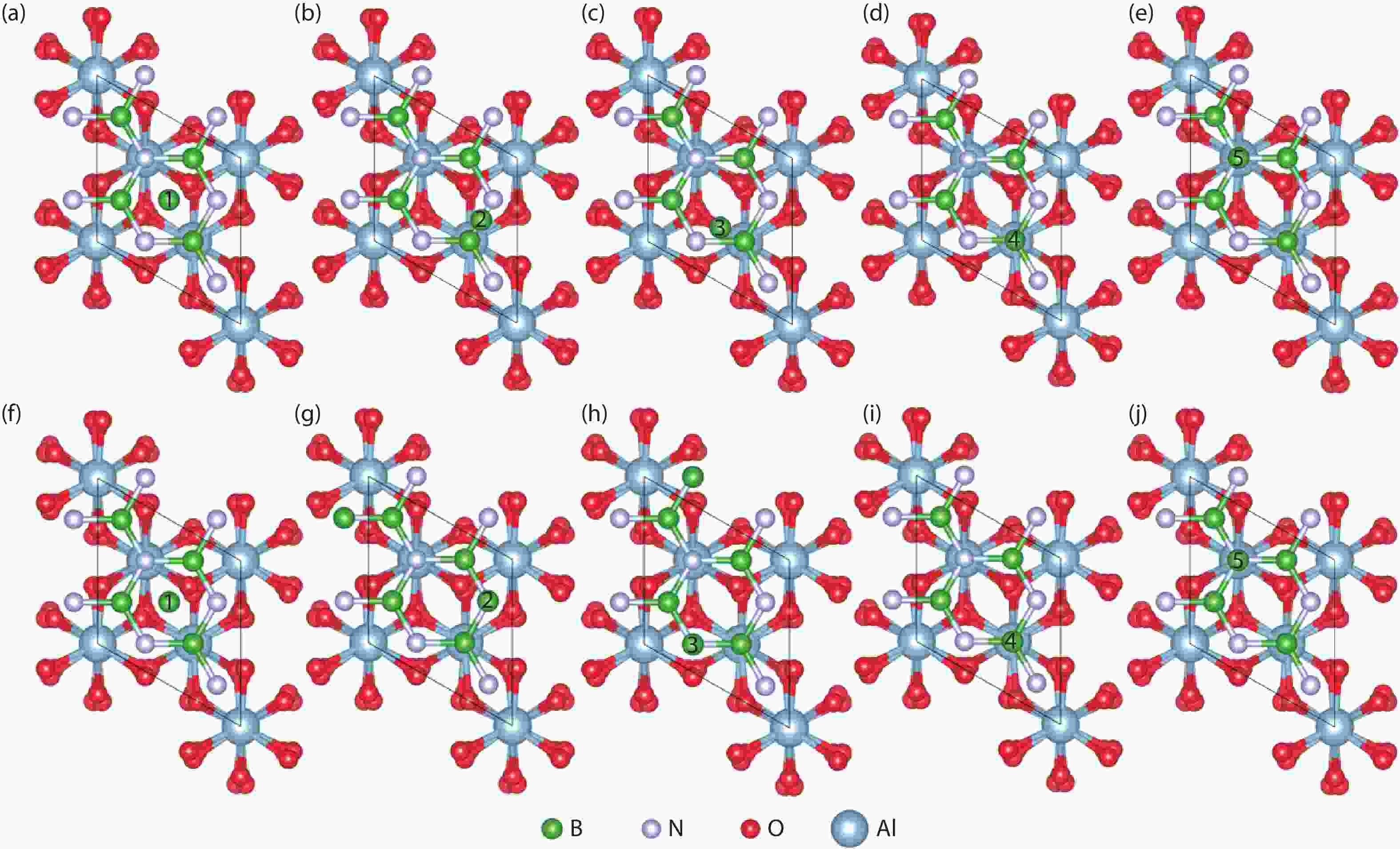
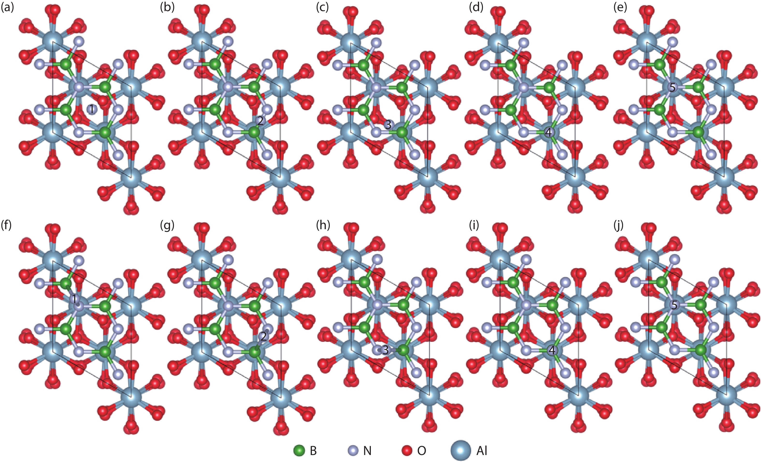
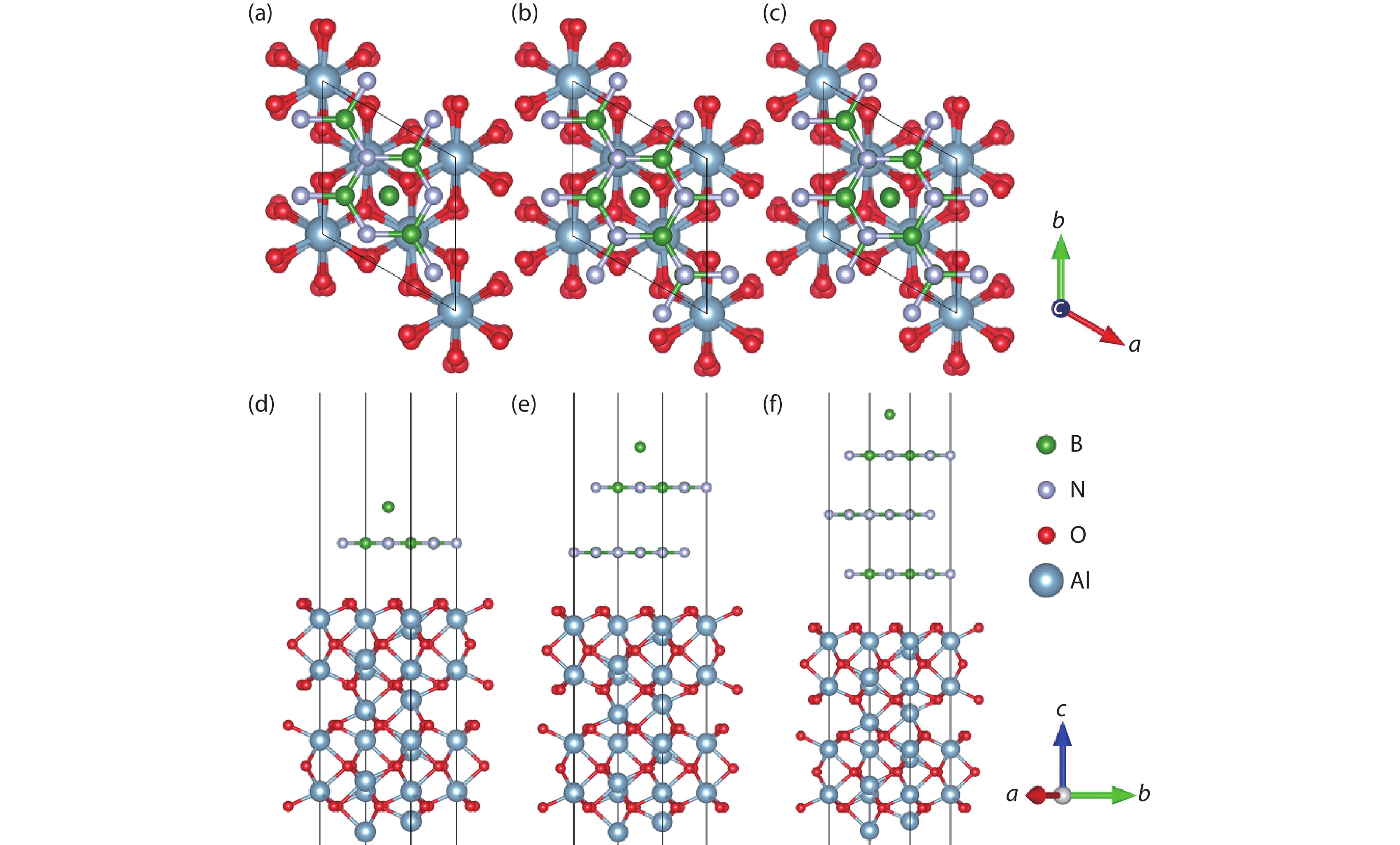
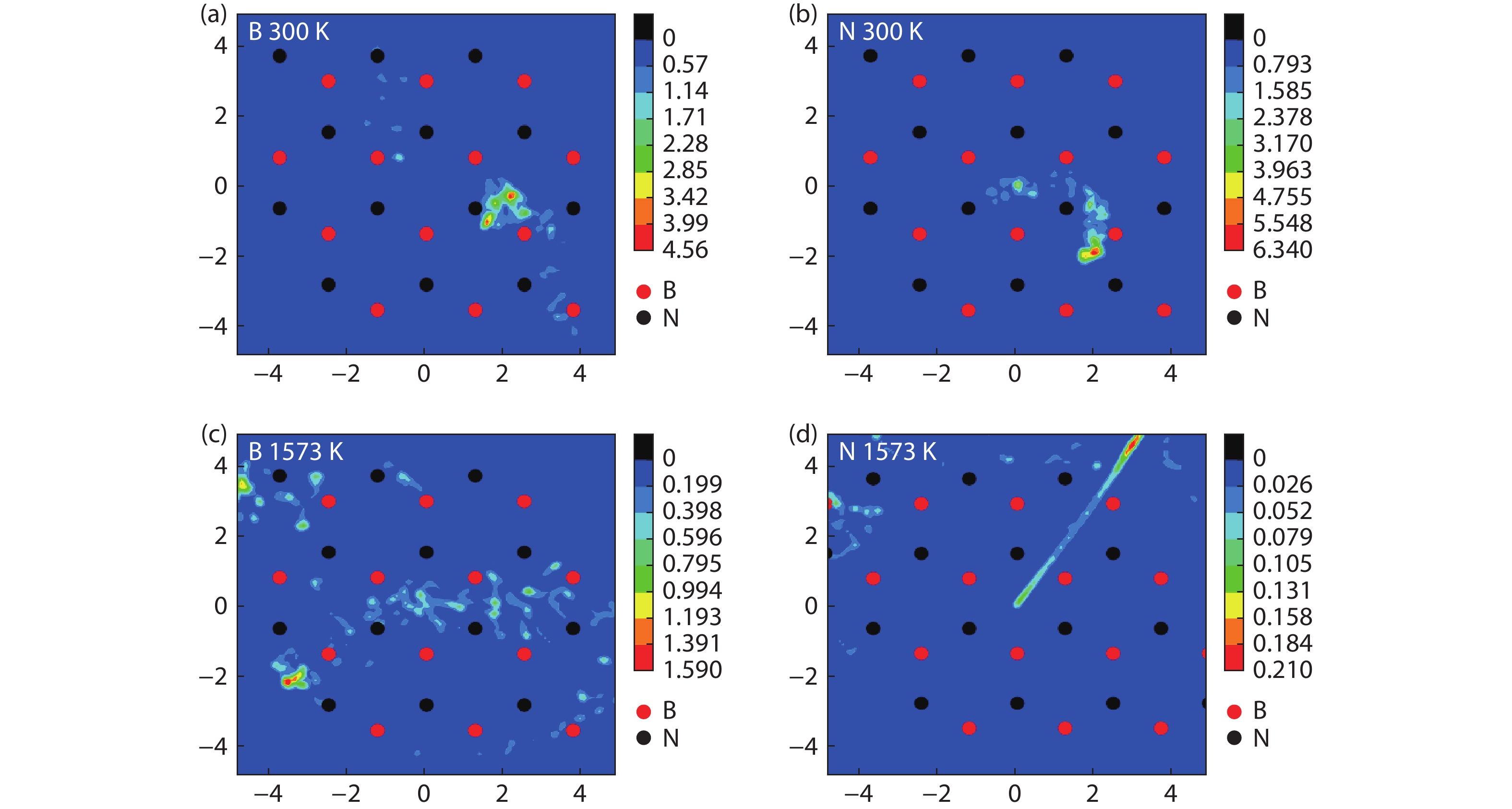
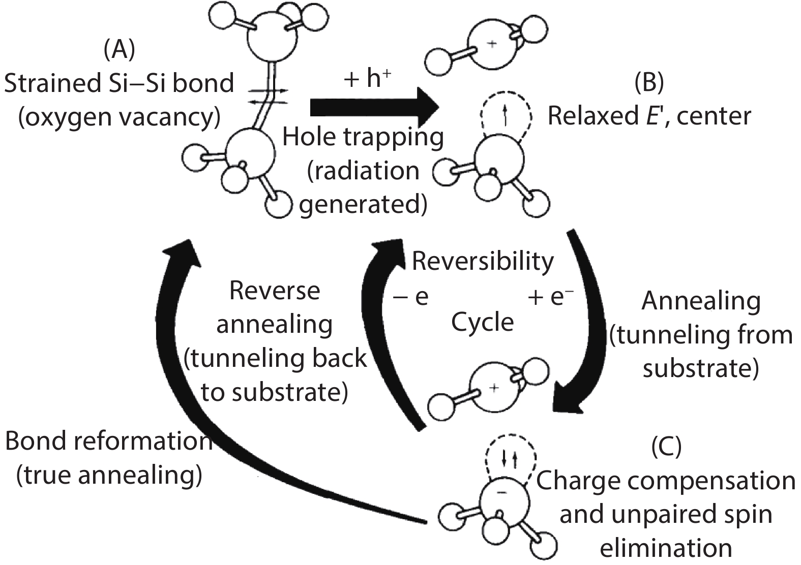
Currently, the preparation of large-size and high-quality hexagonal boron nitride is still an urgent problem. In this study, we investigated the growth and diffusion of boron and nitrogen atoms on the sapphire/h-BN buffer layer by first-principles calculations based on density functional theory. The surface of the single buffer layer provides several metastable adsorption sites for free B and N atoms due to exothermic reaction. The adsorption sites at the ideal growth point for B atoms have the lowest adsorption energy, but the N atoms are easily trapped by the N atoms on the surface to form N–N bonds. With the increasing buffer layers, the adsorption process of free atoms on the surface changes from exothermic to endothermic. The diffusion rate of B atoms is much higher than that of the N atoms thus the B atoms play a major role in the formation of B–N bonds. The introduction of buffer layers can effectively shield the negative effect of sapphire on the formation of B–N bonds. This makes the crystal growth on the buffer layer tends to two-dimensional growth, beneficial to the uniform distribution of B and N atoms. These findings provide an effective reference for the h-BN growth.


J. Semicond.
2021, 42(8): 082802 doi: 10.1088/1674-4926/42/8/082802
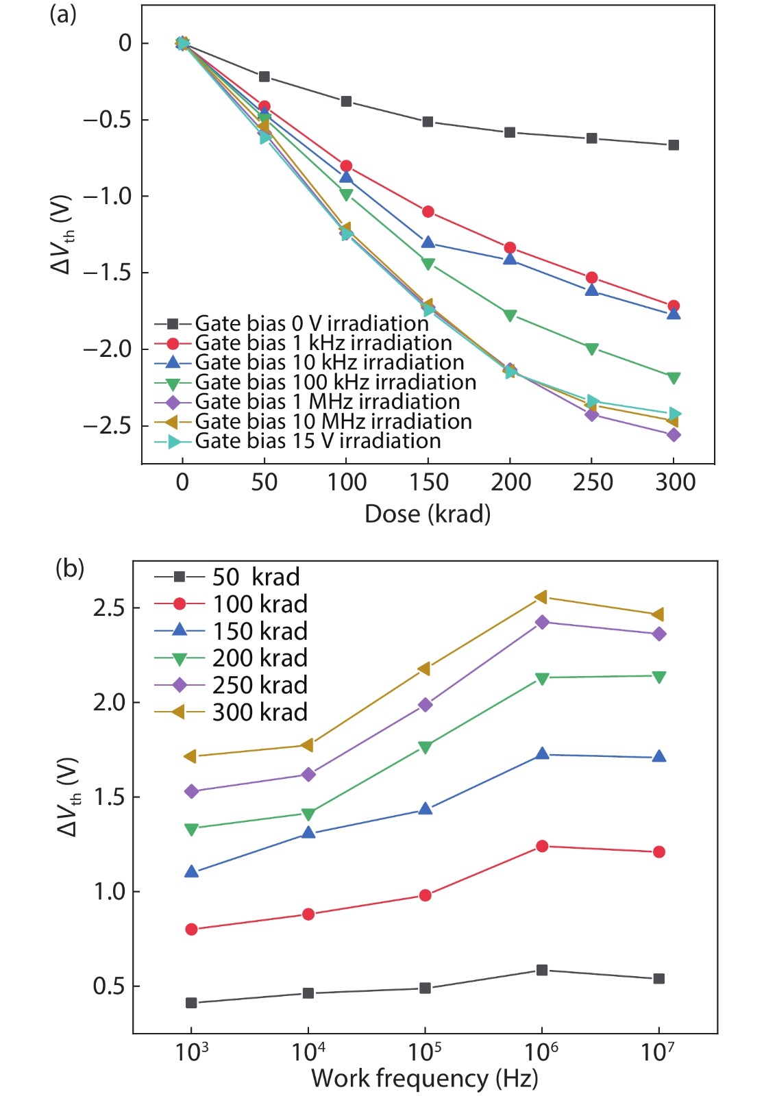
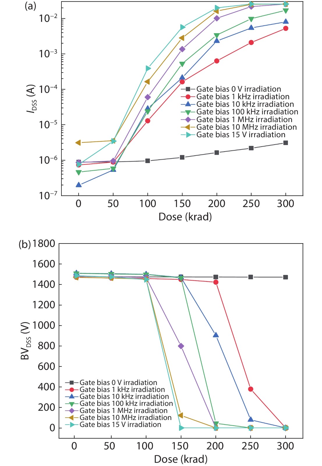
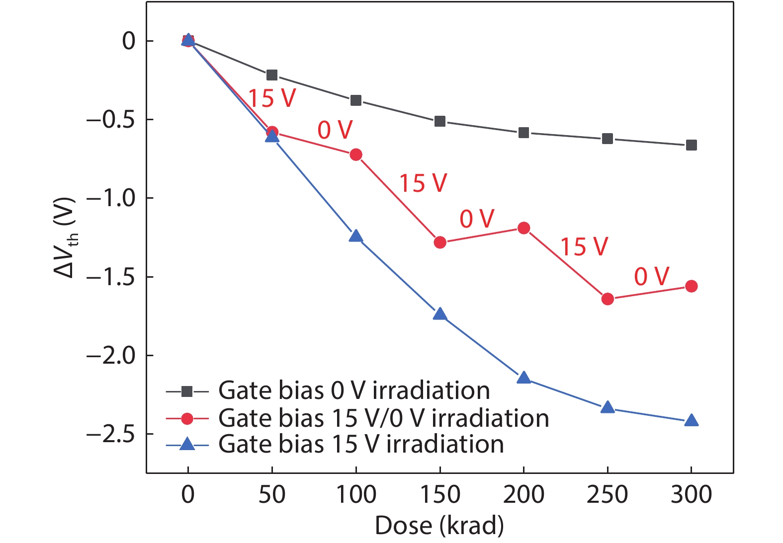
Different switching frequencies are required when SiC metal–oxide–semiconductor field-effect transistors (MOSFETs) are switching in a space environment. In this study, the total ionizing dose (TID) responses of SiC power MOSFETs are investigated under different switching frequencies from 1 kHz to 10 MHz. A significant shift was observed in the threshold voltage as the frequency increased, which resulted in premature failure of the drain–source breakdown voltage and drain–source leakage current. The degradation is attributed to the high activation and low recovery rates of traps at high frequencies. The results of this study suggest that a targeted TID irradiation test evaluation method can be developed according to the actual switching frequency of SiC power MOSFETs.
J. Semicond.
2021, 42(8): 082901 doi: 10.1088/1674-4926/42/8/082901

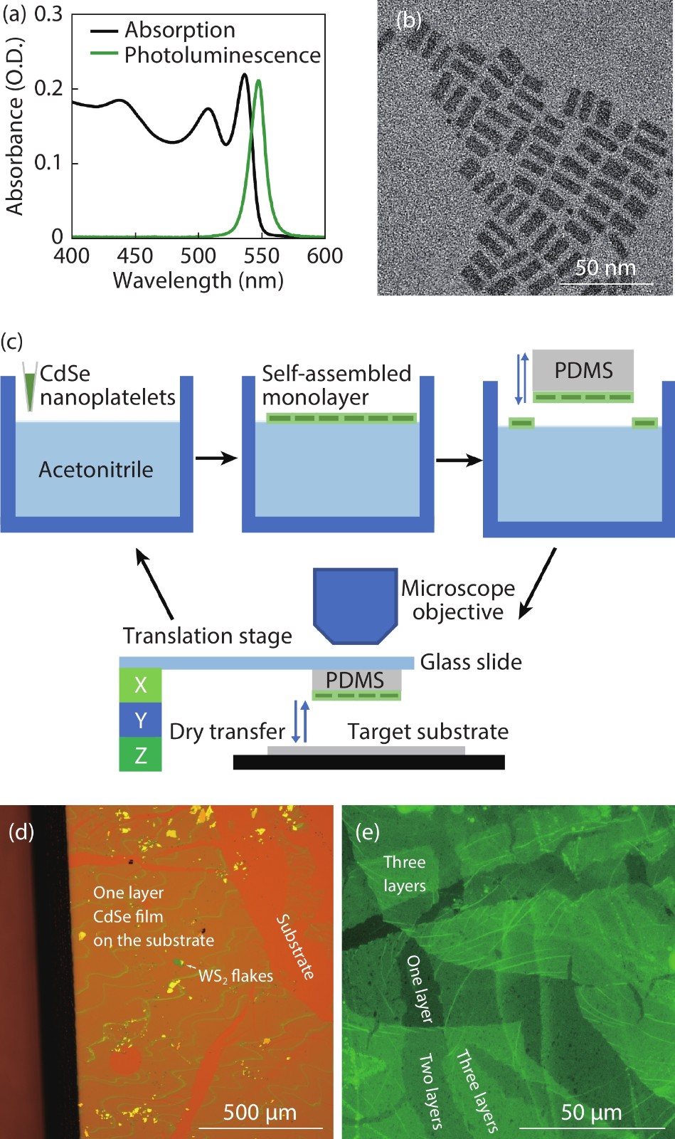
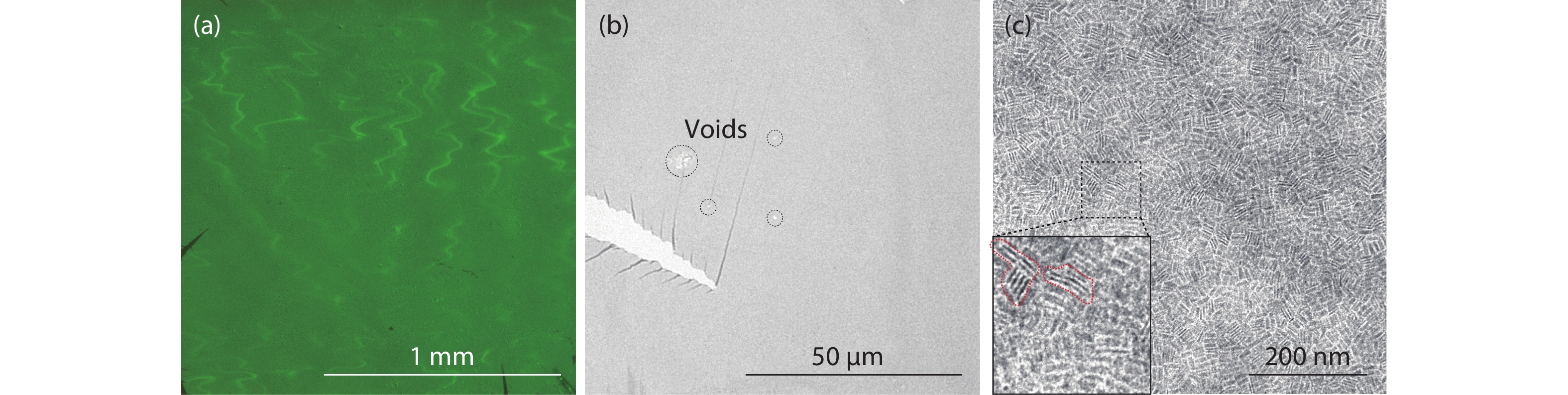
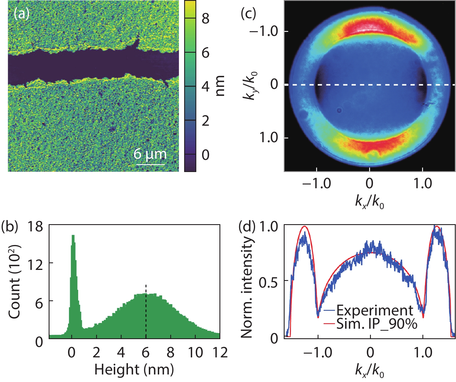
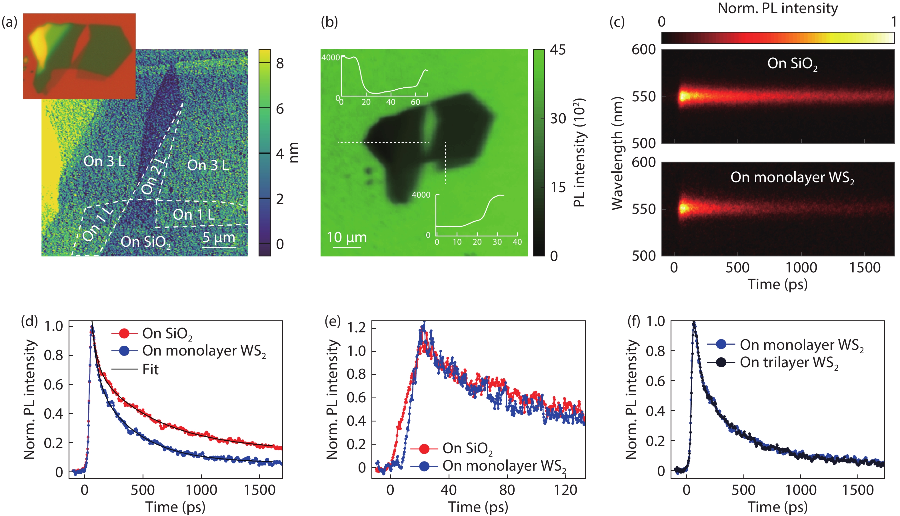
Colloidal CdSe nanoplatelets are thin semiconductor materials with atomic flatness surfaces and one-dimensional strong quantum confinement, and hence they own very narrow and anisotropic emission. Here, we present a polydimethylsiloxane (PDMS) assisted transferring method that can pick up single layer CdSe nanoplatelet films self-assembled on a liquid surface and then precisely transfer to a target. By layer-by-layer picking up and transferring, multiple layers of CdSe films can be built up to form CdSe stacks with each single layer having dominant in-plane transition dipole distribution, which both material and energic structures are analogous to traditional multiple quantum wells grown by molecular-beam epitaxy. Additionally, with the great flexibility of colloidal nanoplatelets and this transferring method, CdSe nanoplatelets films can be combined with other materials to form hybrid heterostructures. We transferred a single-layer CdSe film onto WS2 flakes, and precisely studied the fast energy transfer rate with controlled CdSe nanoplatelet orientation and by using a streak camera with a ps time resolution.
J. Semicond.
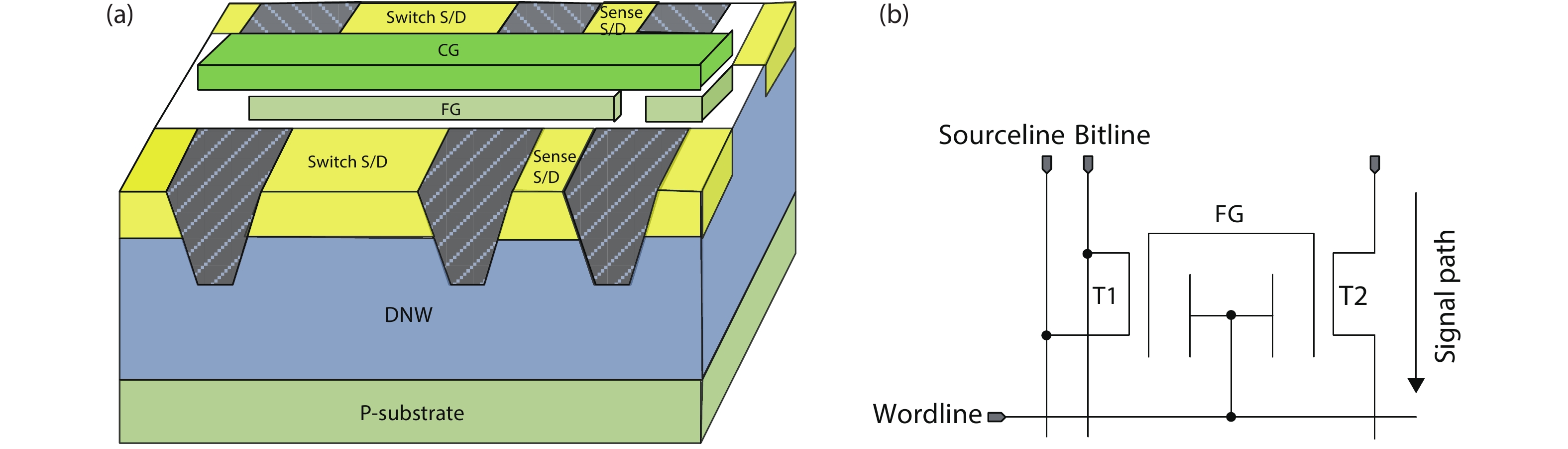
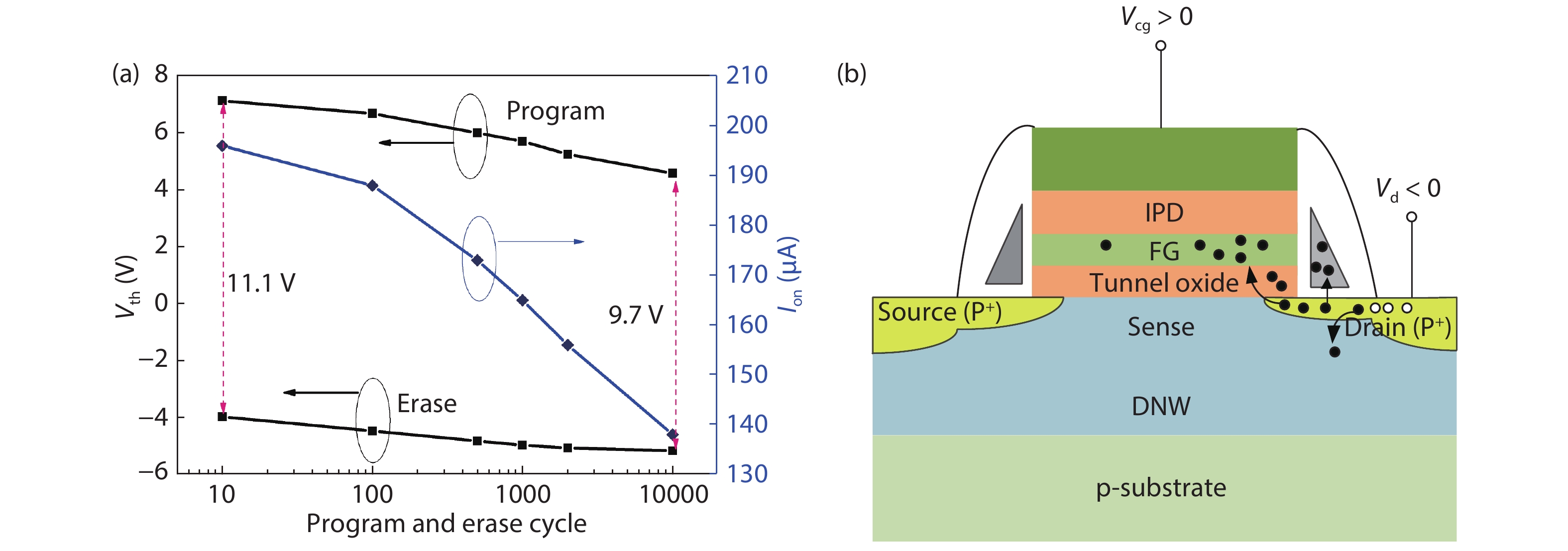
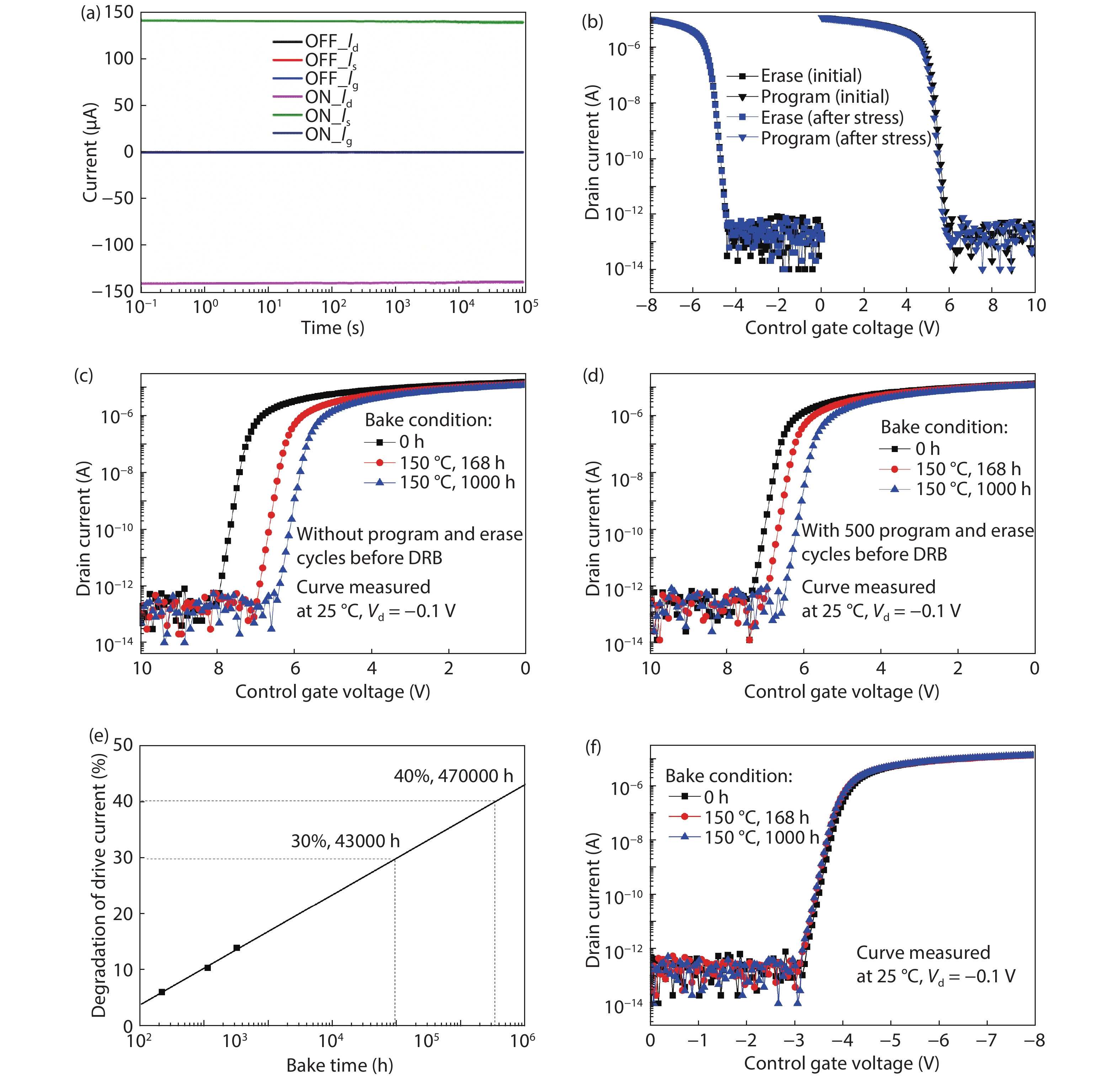
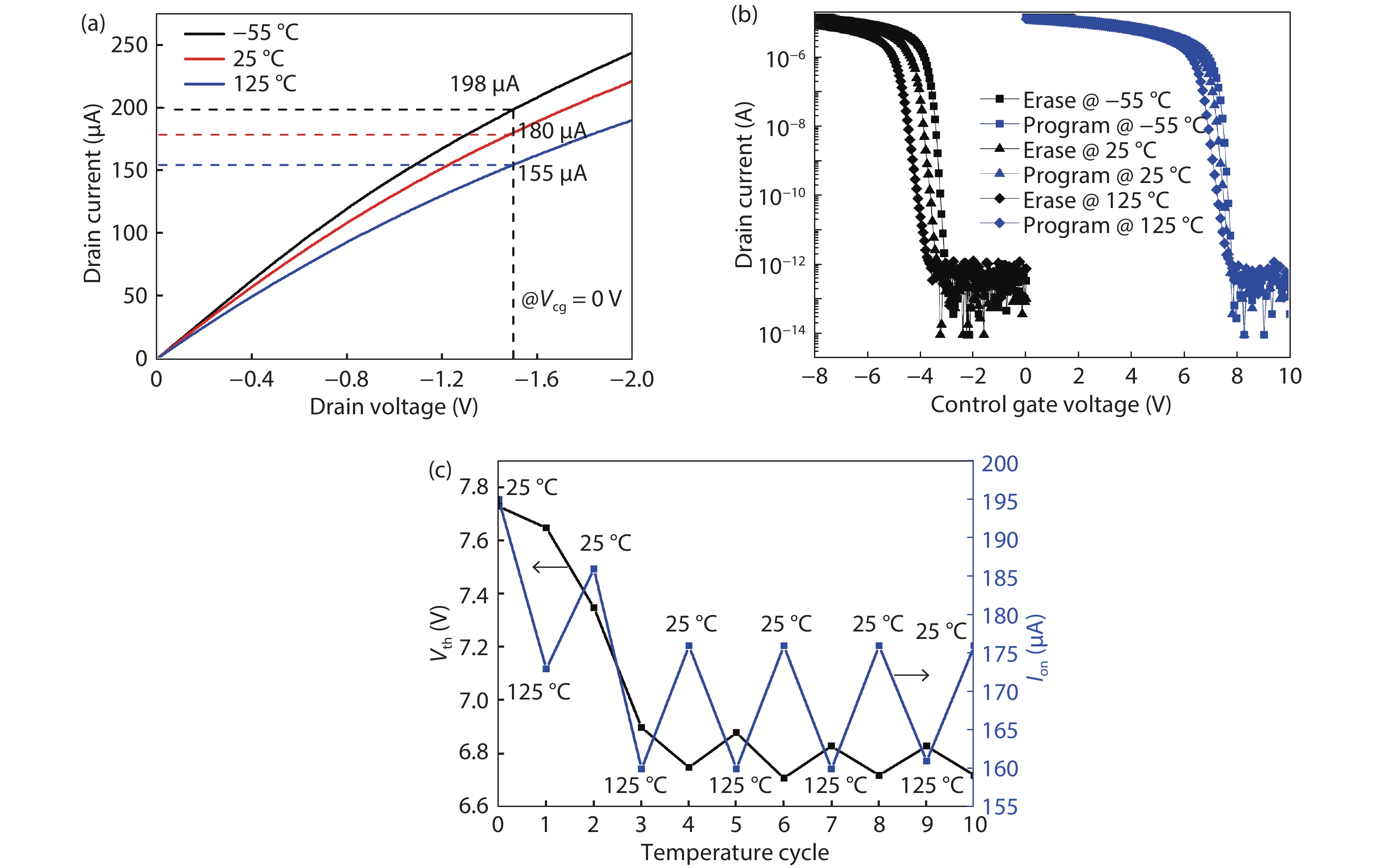
2021, 42(8): 084101 doi: 10.1088/1674-4926/42/8/084101
In this paper, the reliability of sense-switch p-channel flash is evaluated extensively. The endurance result indicates that the p-channel flash could be programmed and erased for more than 10 000 cycles; the room temperature read stress shows negligible influence on the p-channel flash cell; high temperature data retention at 150 °C is extrapolated to be about 5 years and 53 years corresponding to 30% and 40% degradation in the drive current, respectively. Moreover, the electrical parameters of the p-channel flash at different operation temperature are found to be less affected. All the results above indicate that the sense-switch p-channel flash is suitable to be used as the configuration cell in flash-based FPGA.