Issue Browser
Volume 43, Issue 4,
Apr 2022

J. Semicond.
2022, 43(4): 041101 doi: 10.1088/1674-4926/43/4/041101

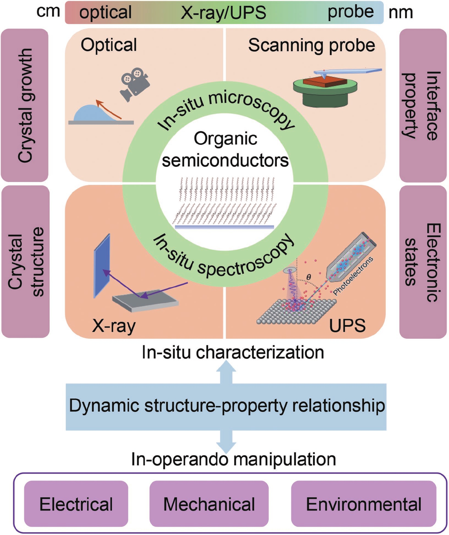
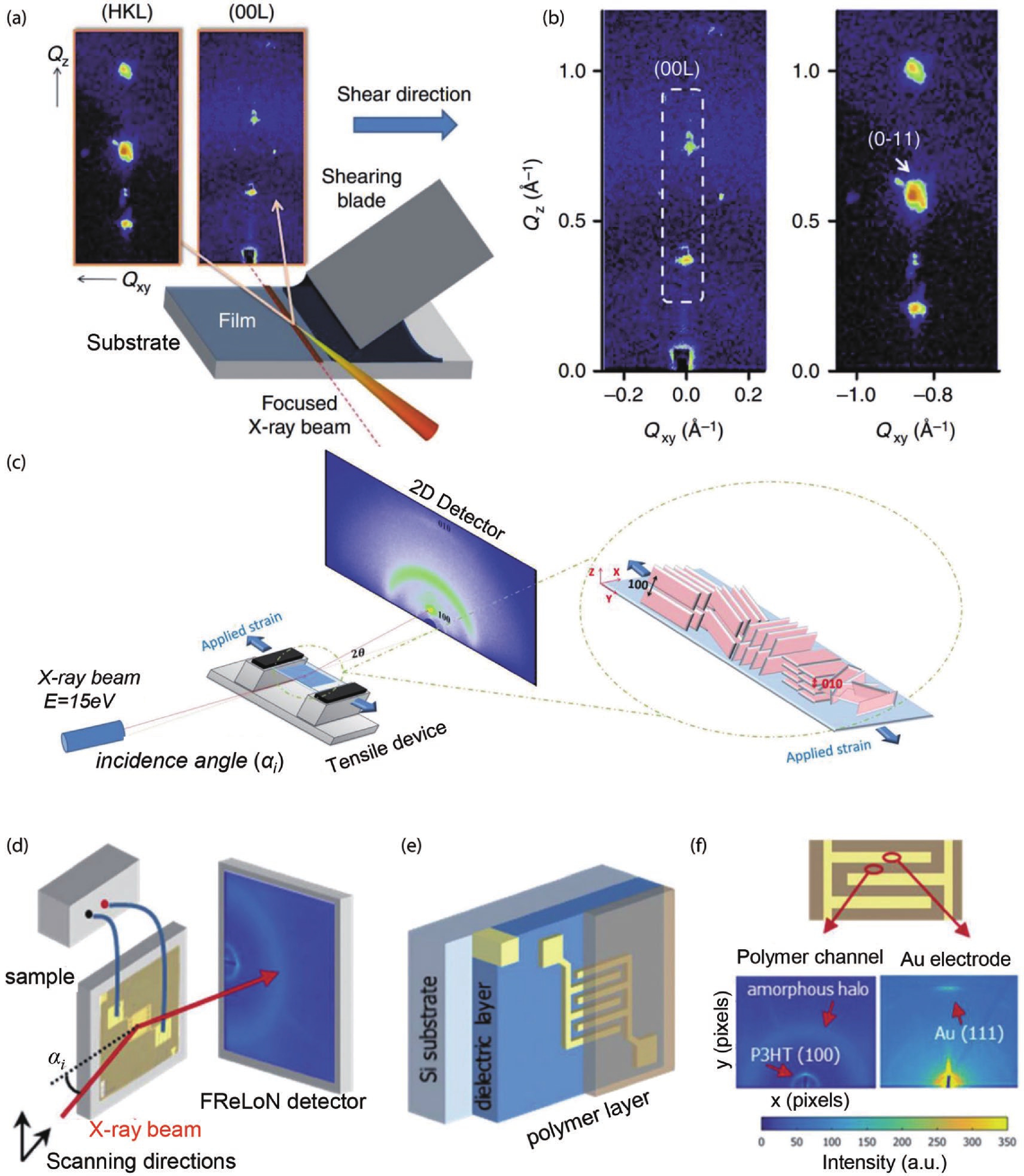
The increasing demands of multifunctional organic electronics require advanced organic semiconducting materials to be developed and significant improvements to be made to device performance. Thus, it is necessary to gain an in-depth understanding of the film growth process, electronic states, and dynamic structure-property relationship under realistic operation conditions, which can be obtained by in-situ/operando characterization techniques for organic devices. Here, the up-to-date developments in the in-situ/operando optical, scanning probe microscopy, and spectroscopy techniques that are employed for studies of film morphological evolution, crystal structures, semiconductor-electrolyte interface properties, and charge carrier dynamics are described and summarized. These advanced technologies leverage the traditional static characterizations into an in-situ and interactive manipulation of organic semiconducting films and devices without sacrificing the resolution, which facilitates the exploration of the intrinsic structure-property relationship of organic materials and the optimization of organic devices for advanced applications.
J. Semicond.
2022, 43(4): 041102 doi: 10.1088/1674-4926/43/4/041102
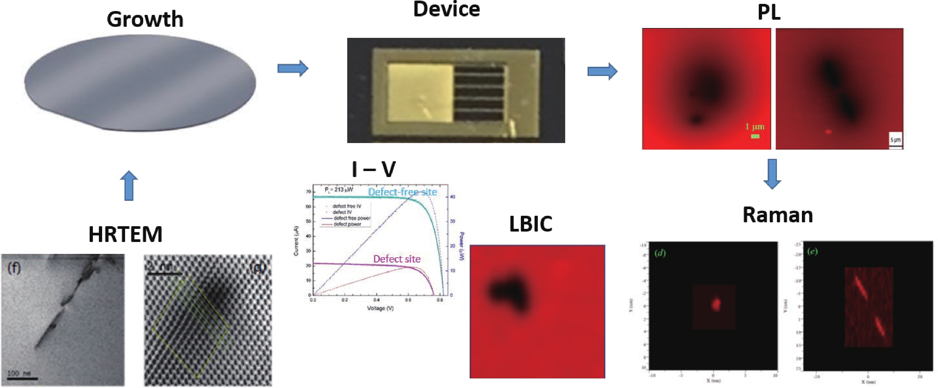
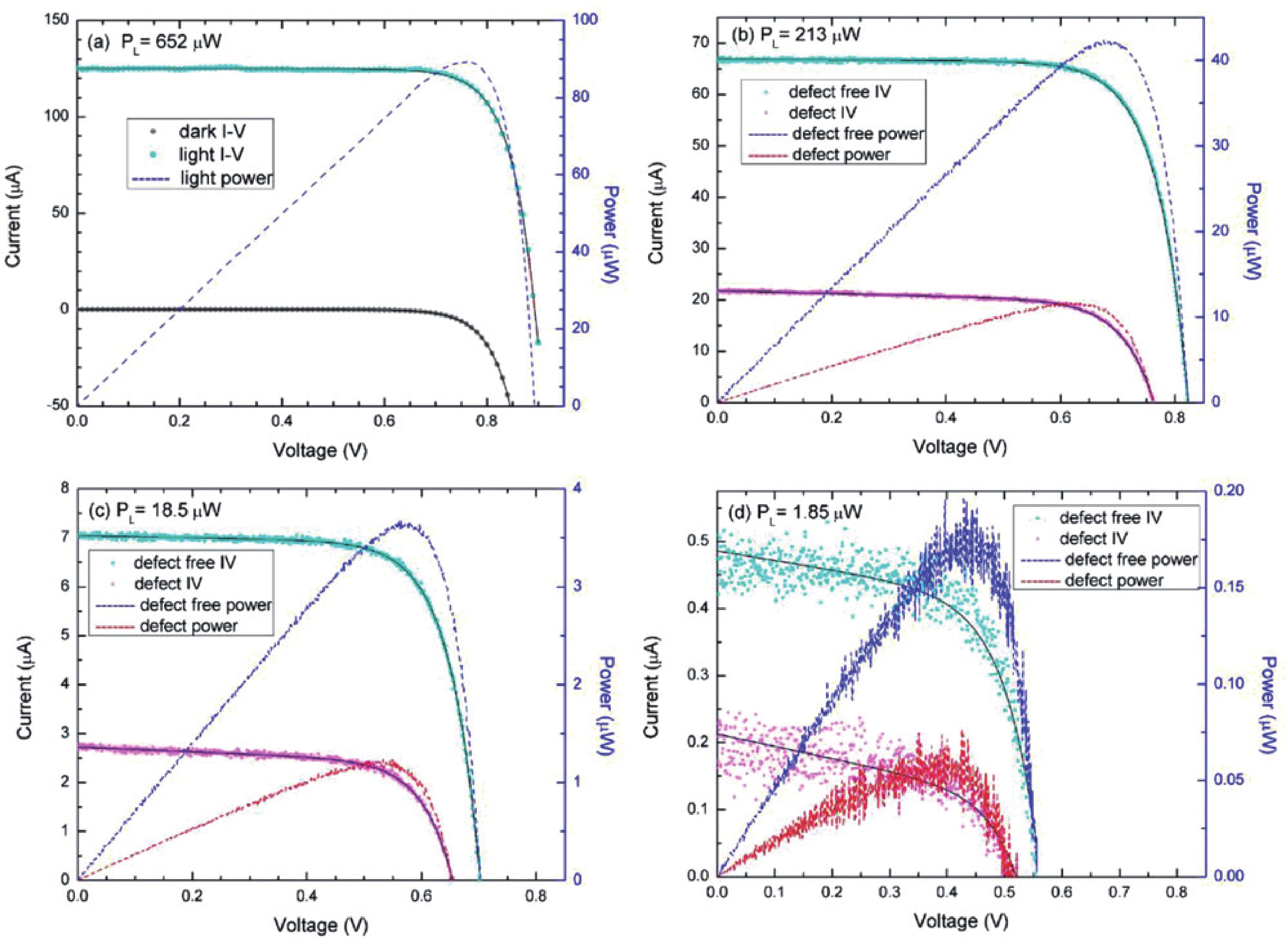
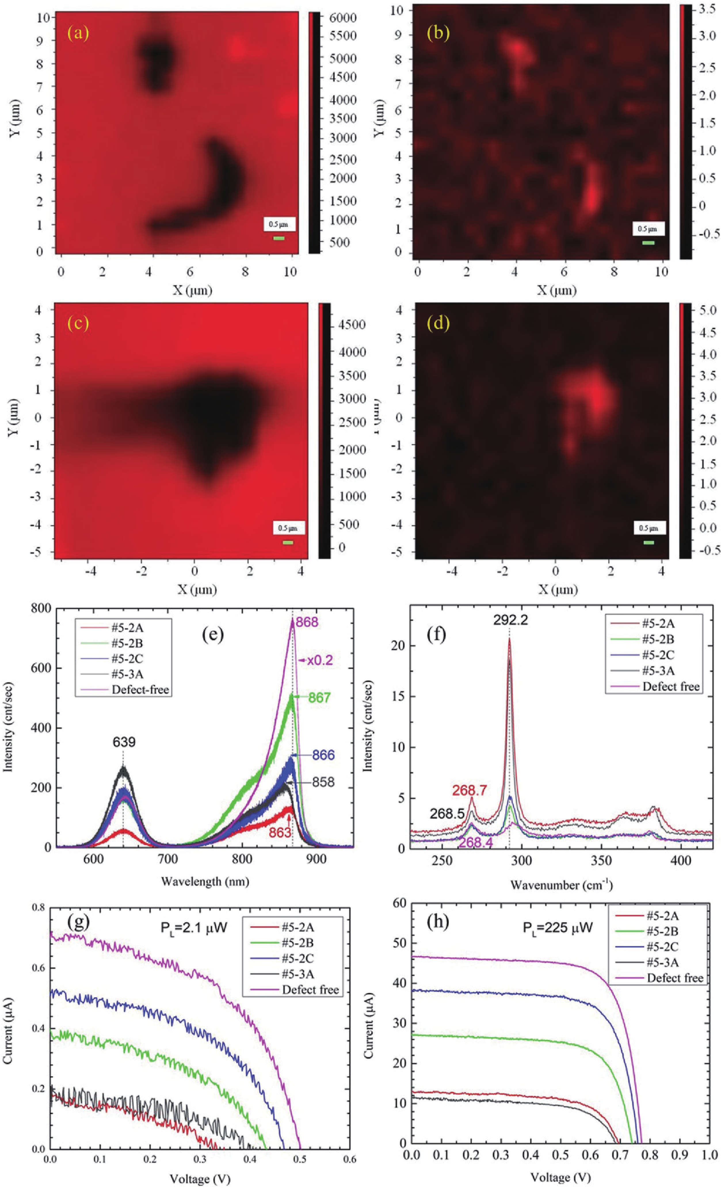
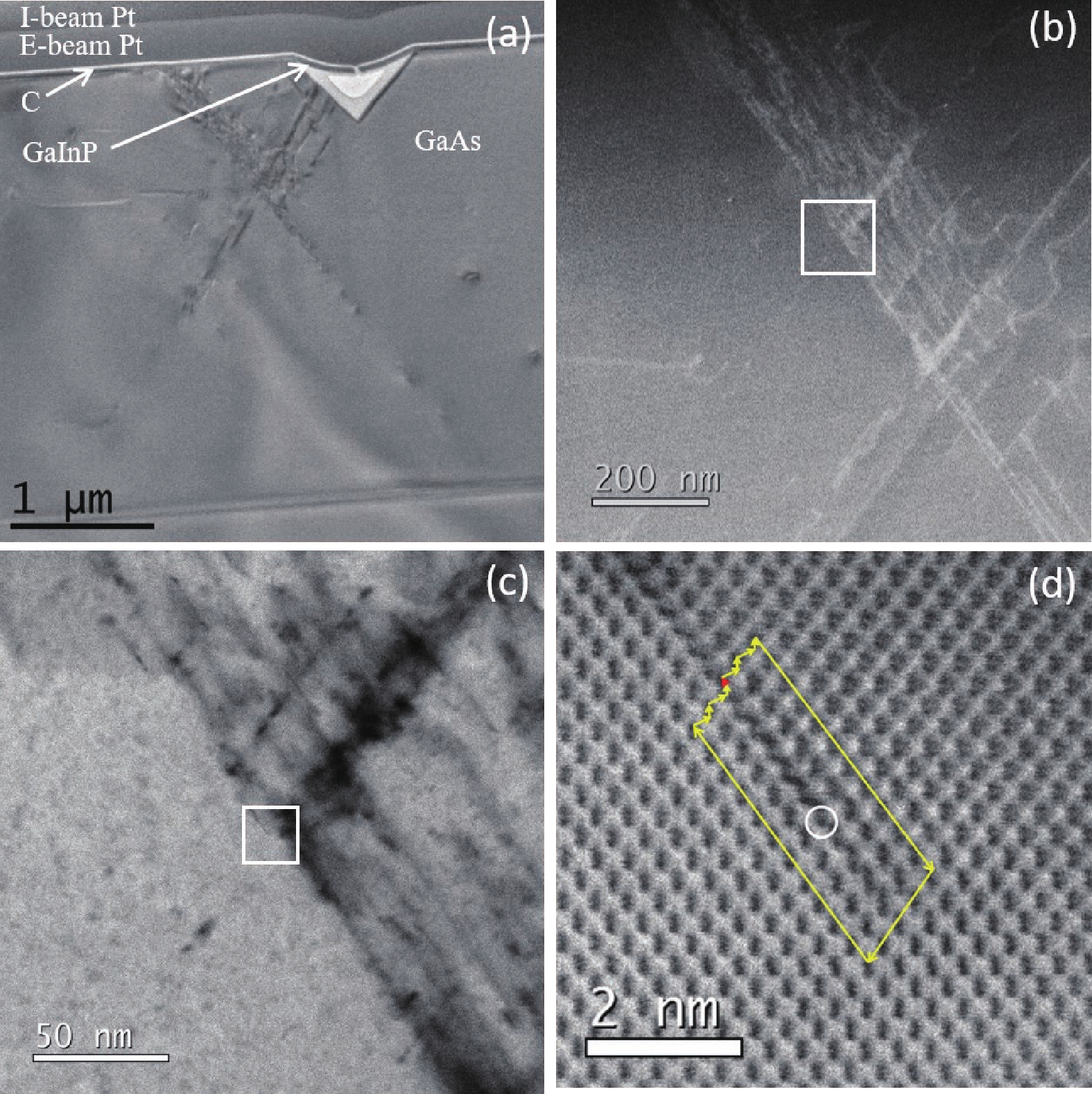
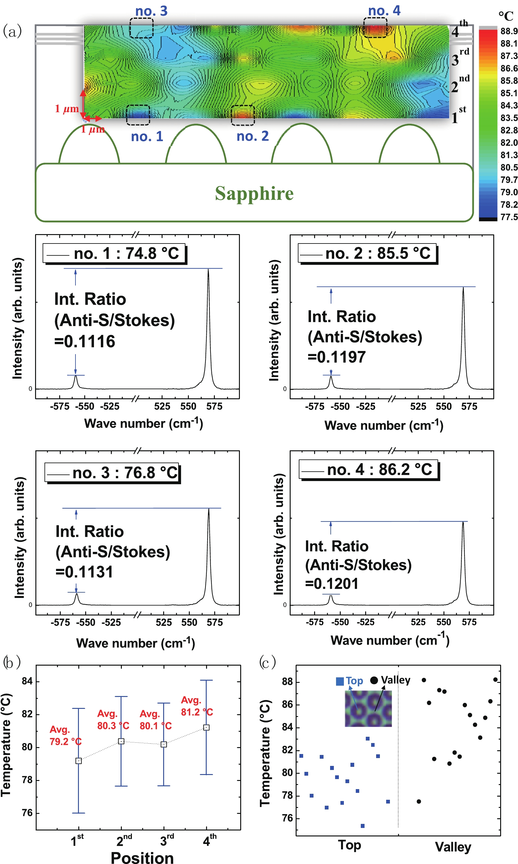
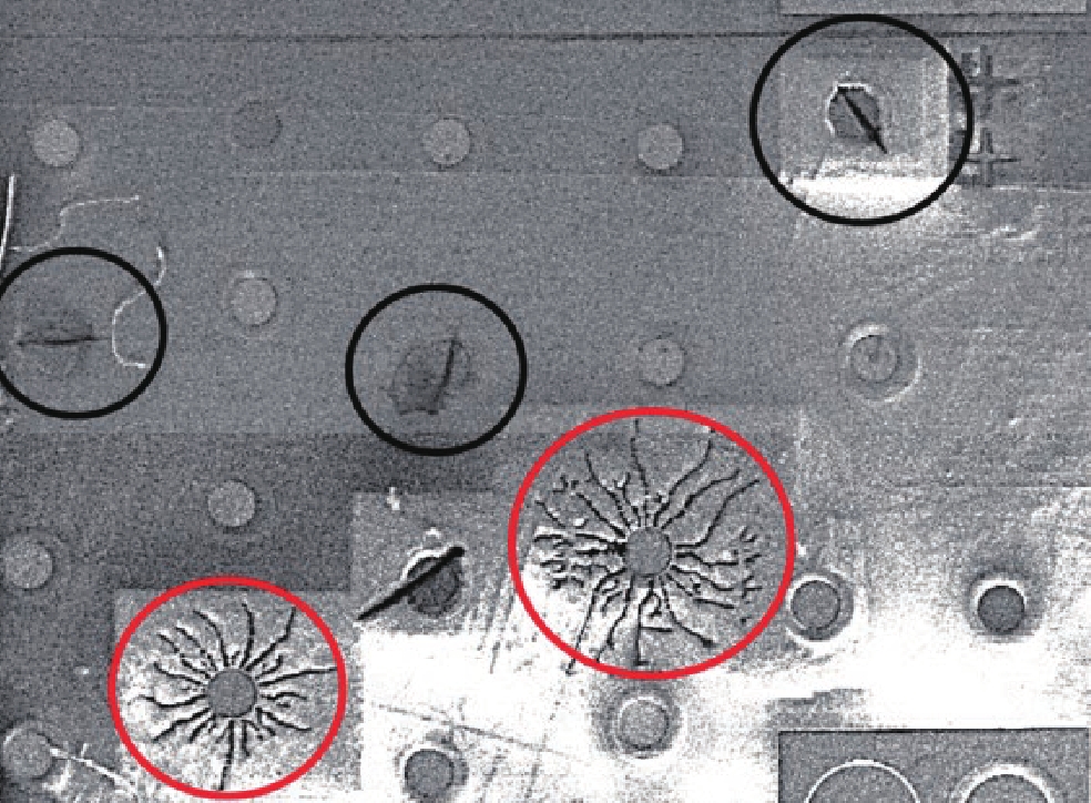
Despite the long history of research that has focused on the role of defects on device performance, the studies have not always been fruitful. A major reason is because these defect studies have typically been conducted in a parallel mode wherein the semiconductor wafer was divided into multiple pieces for separate optical and structural characterization, as well as device fabrication and evaluation. The major limitation of this approach was that either the defect being investigated by structural characterization techniques was not the same defect that was affecting the device performance or else the defect was not characterized under normal device operating conditions. In this review, we describe a more comprehensive approach to defect study, namely a series mode, using an array of spatially-resolved optical, electrical, and structural characterization techniques, all at the individual defect level but applied sequentially on a fabricated device. This novel sequential approach enables definitive answers to key questions, such as: (i) how do individual defects affect device performance? (ii) how does the impact depend on the device operation conditions? (iii) how does the impact vary from one defect to another? Implementation of this different approach is illustrated by the study of individual threading dislocation defects in GaAs solar cells. Additionally, we briefly describe a 3-D Raman thermometry method that can also be used for investigating the roles of defects in high power devices and device failure mechanisms.


J. Semicond.
2022, 43(4): 041103 doi: 10.1088/1674-4926/43/4/041103
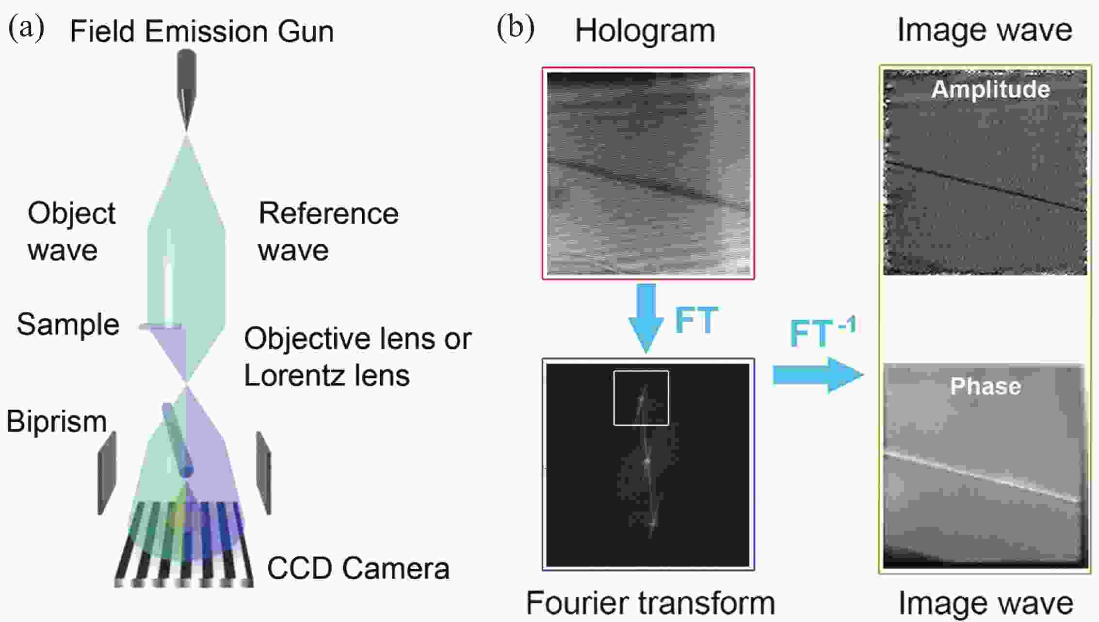
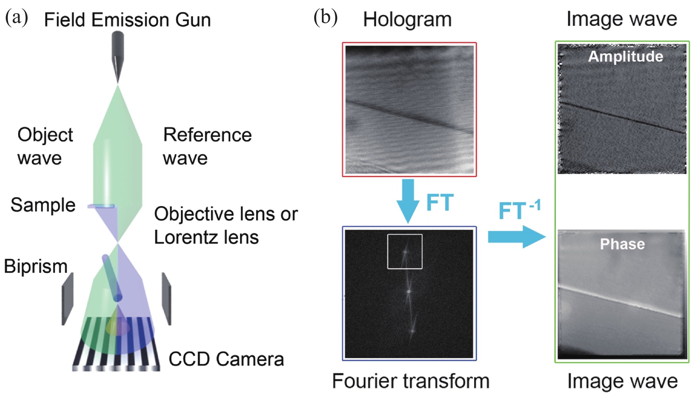
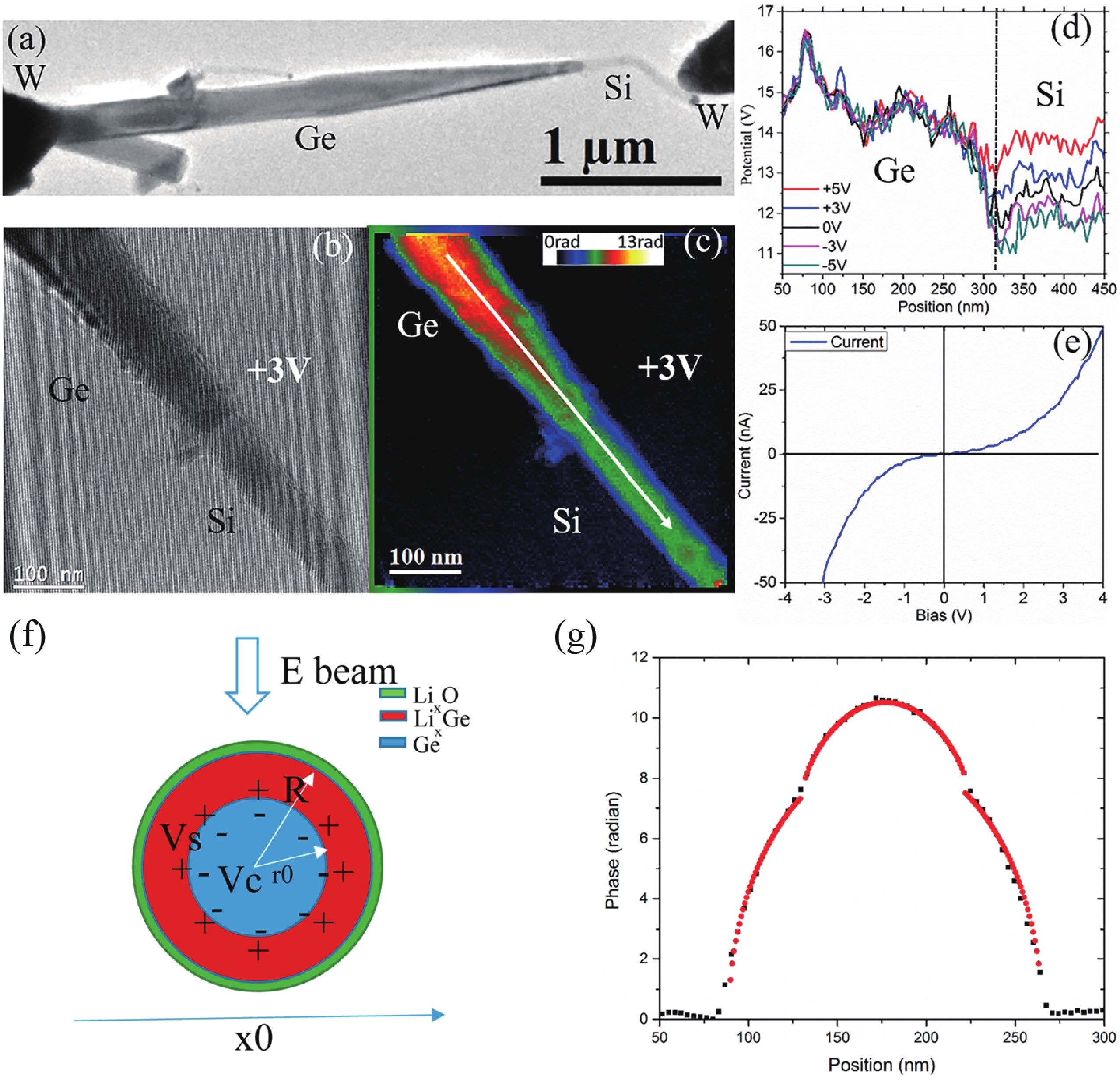
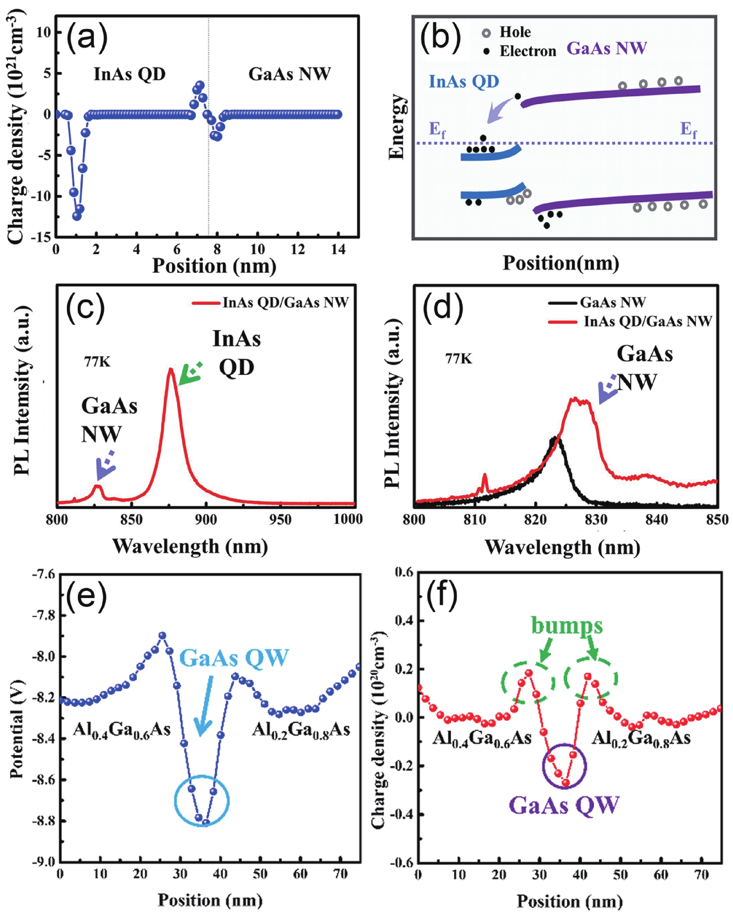
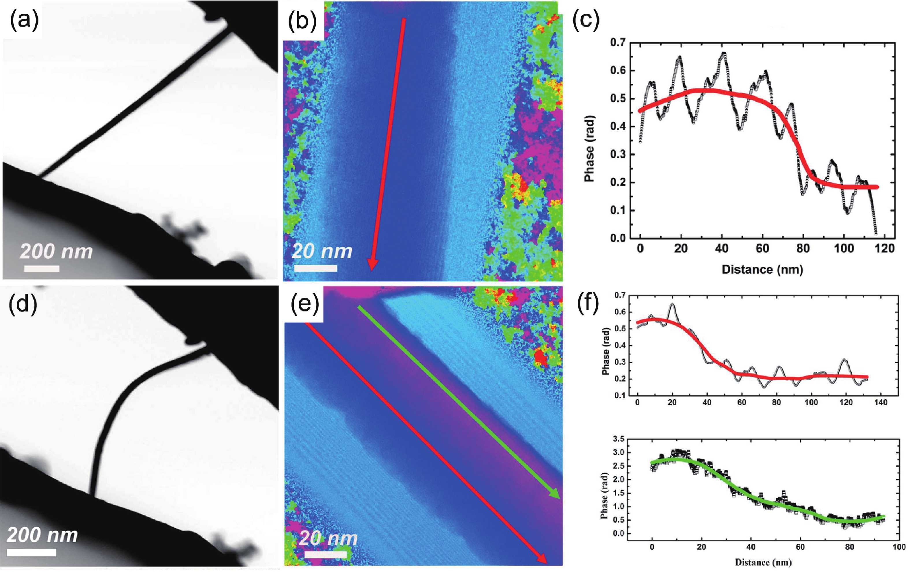
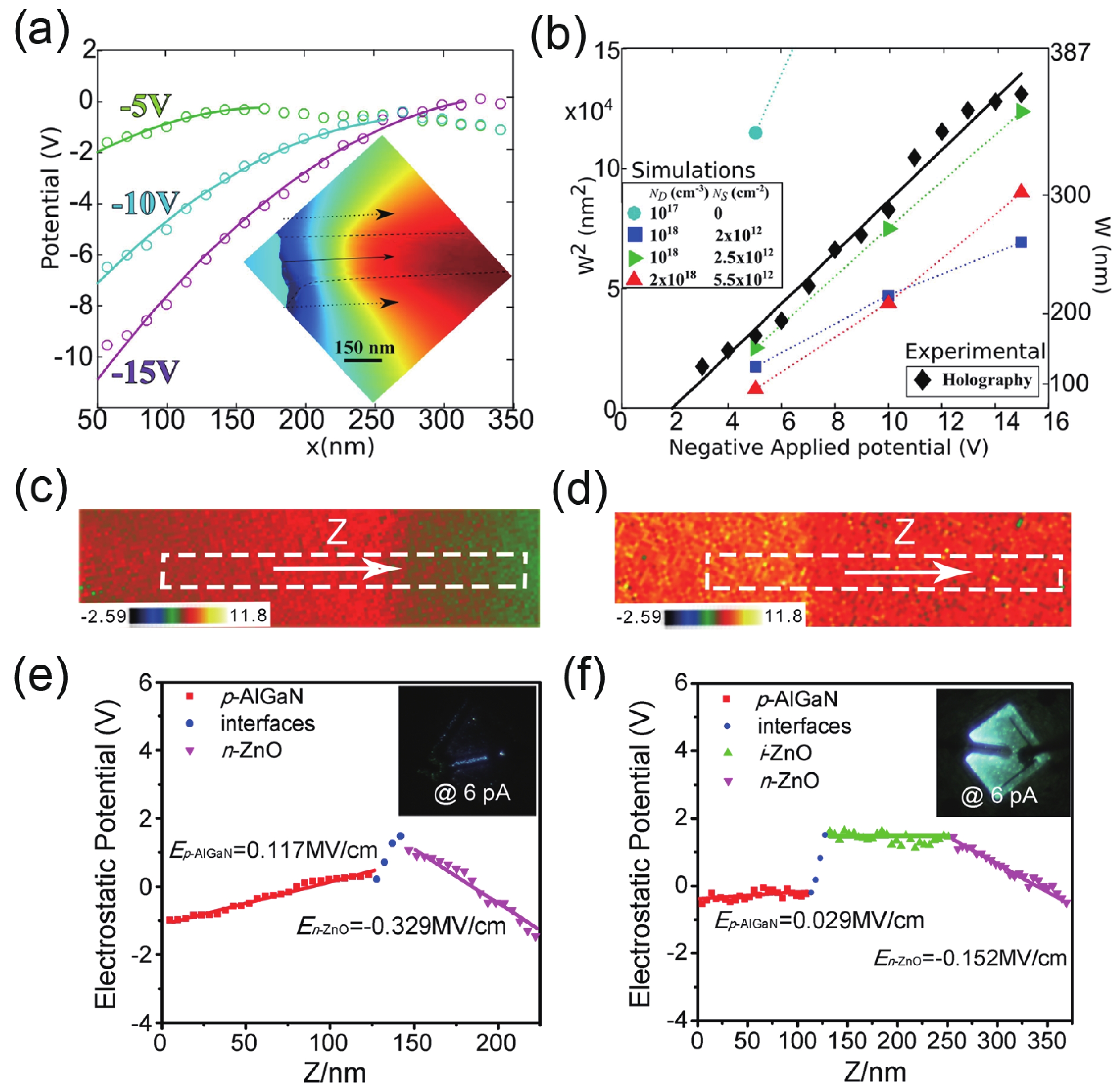
As the scaling down of semiconductor devices, it would be necessary to discover the structure-property relationship of semiconductor nanomaterials at nanometer scale. In this review, the quantitative characterization technique off-axis electron holography is introduced in details, followed by its applications in various semiconductor nanomaterials including group IV, compound and two-dimensional semiconductor nanostructures in static states as well as under various stimuli. The advantages and disadvantages of off-axis electron holography in material analysis are discussed, the challenges facing in-situ electron holographic study of semiconductor devices at working conditions are presented, and all the possible influencing factors need to be considered to achieve the final goal of fulfilling quantitative characterization of the structure-property relationship of semiconductor devices at their working conditions.


J. Semicond.
2022, 43(4): 041104 doi: 10.1088/1674-4926/43/4/041104
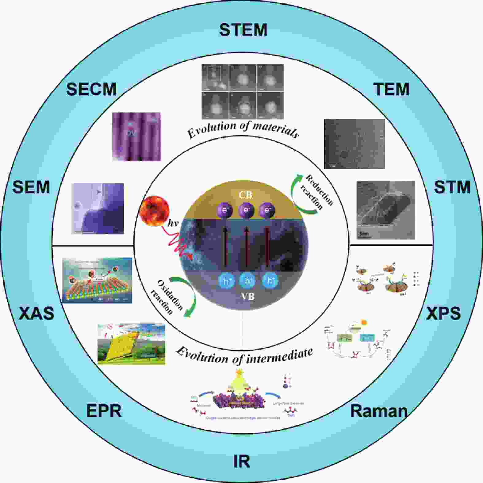
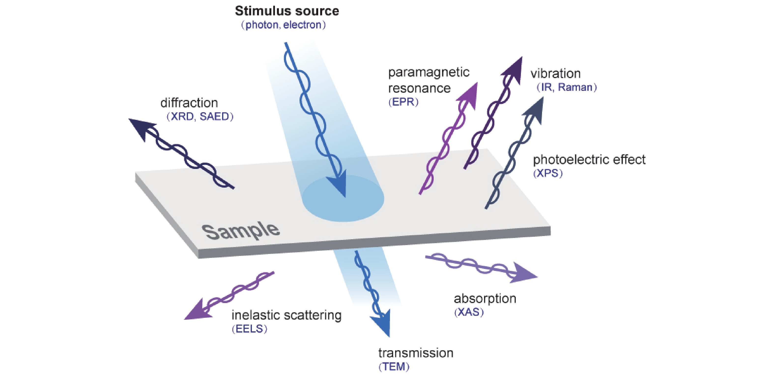
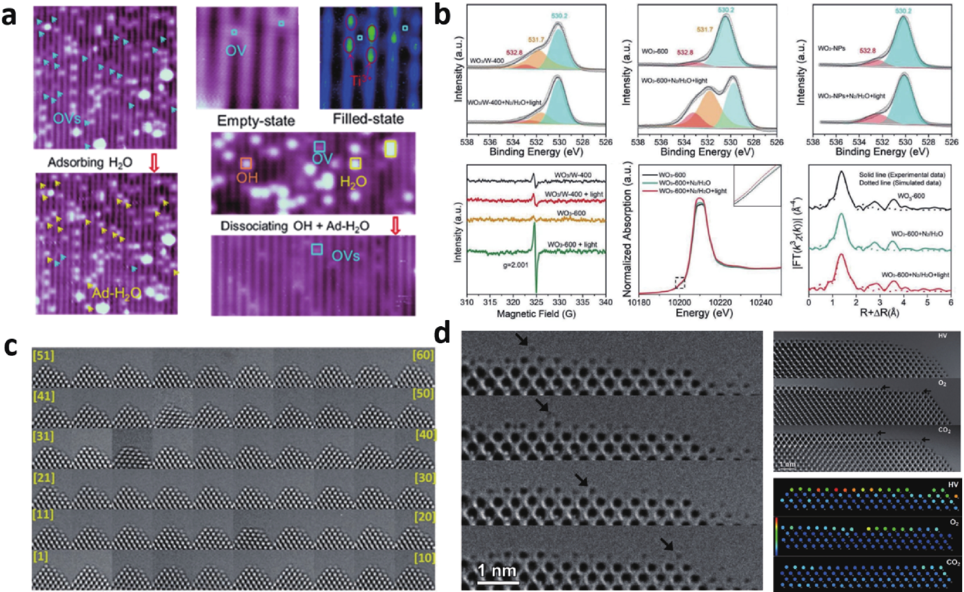
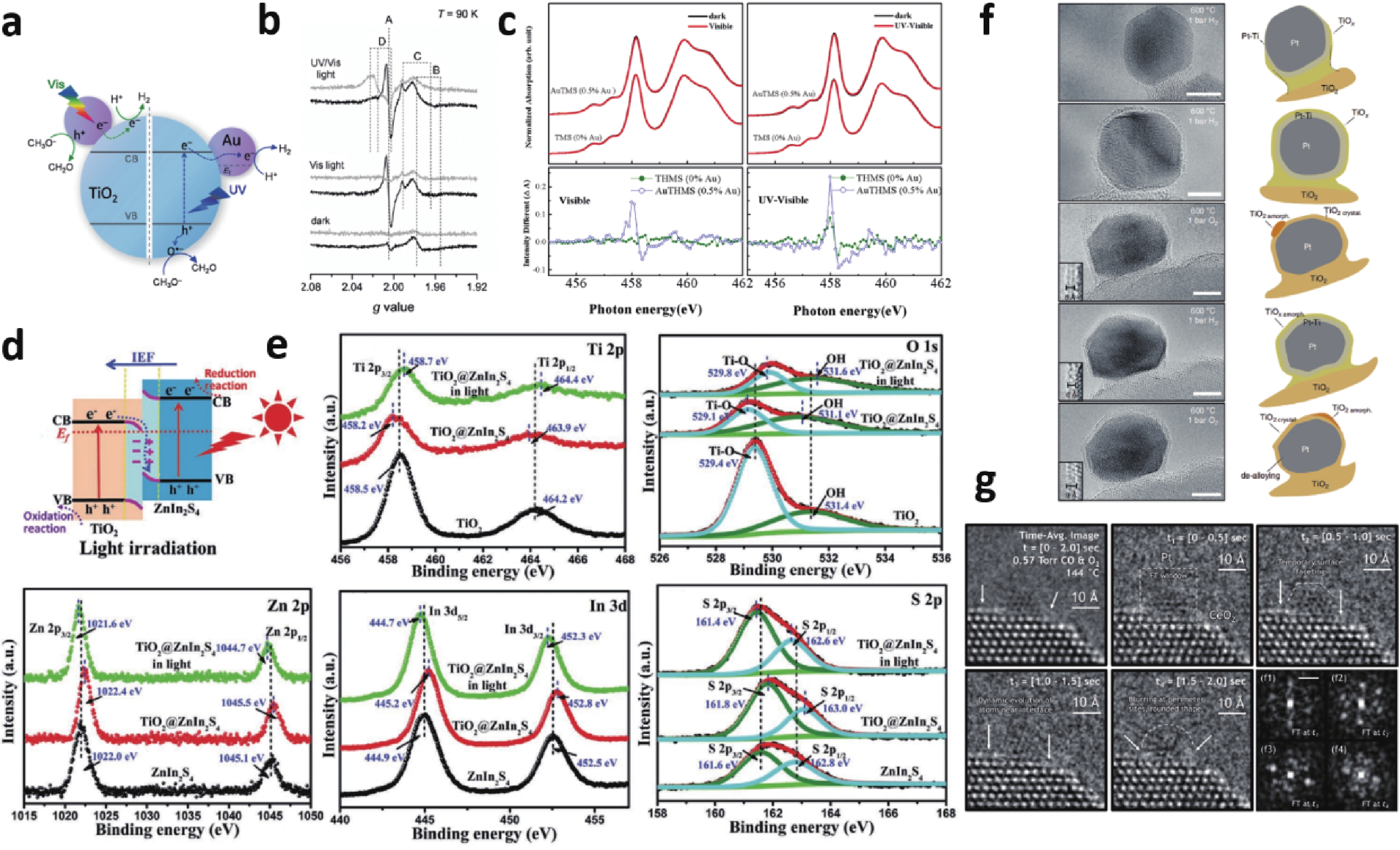
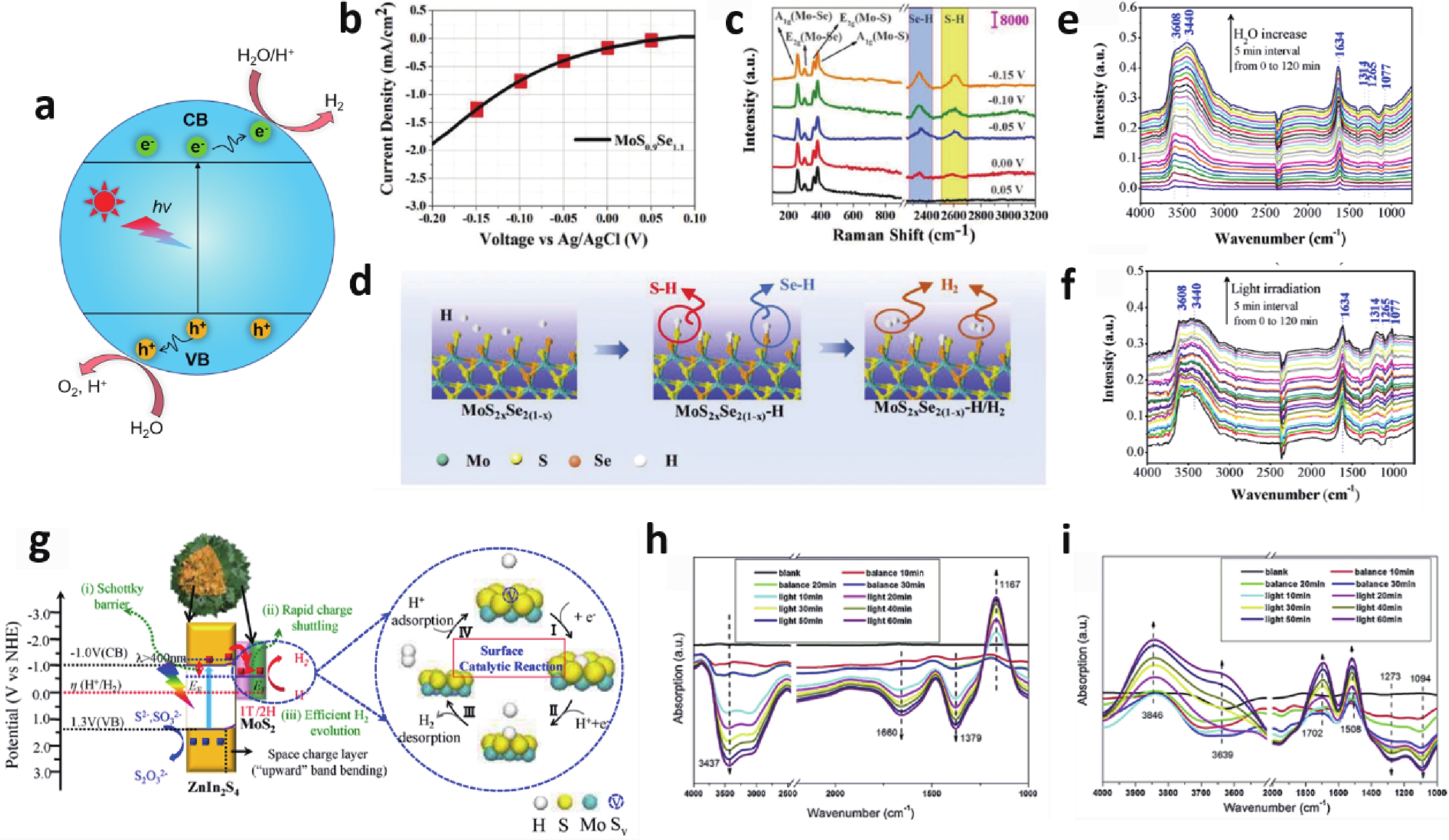
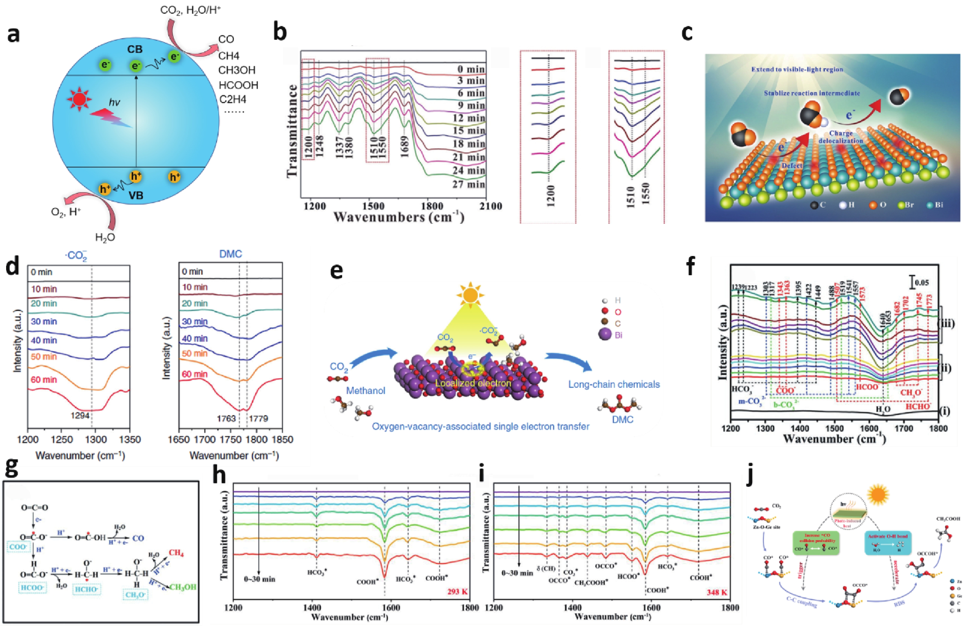
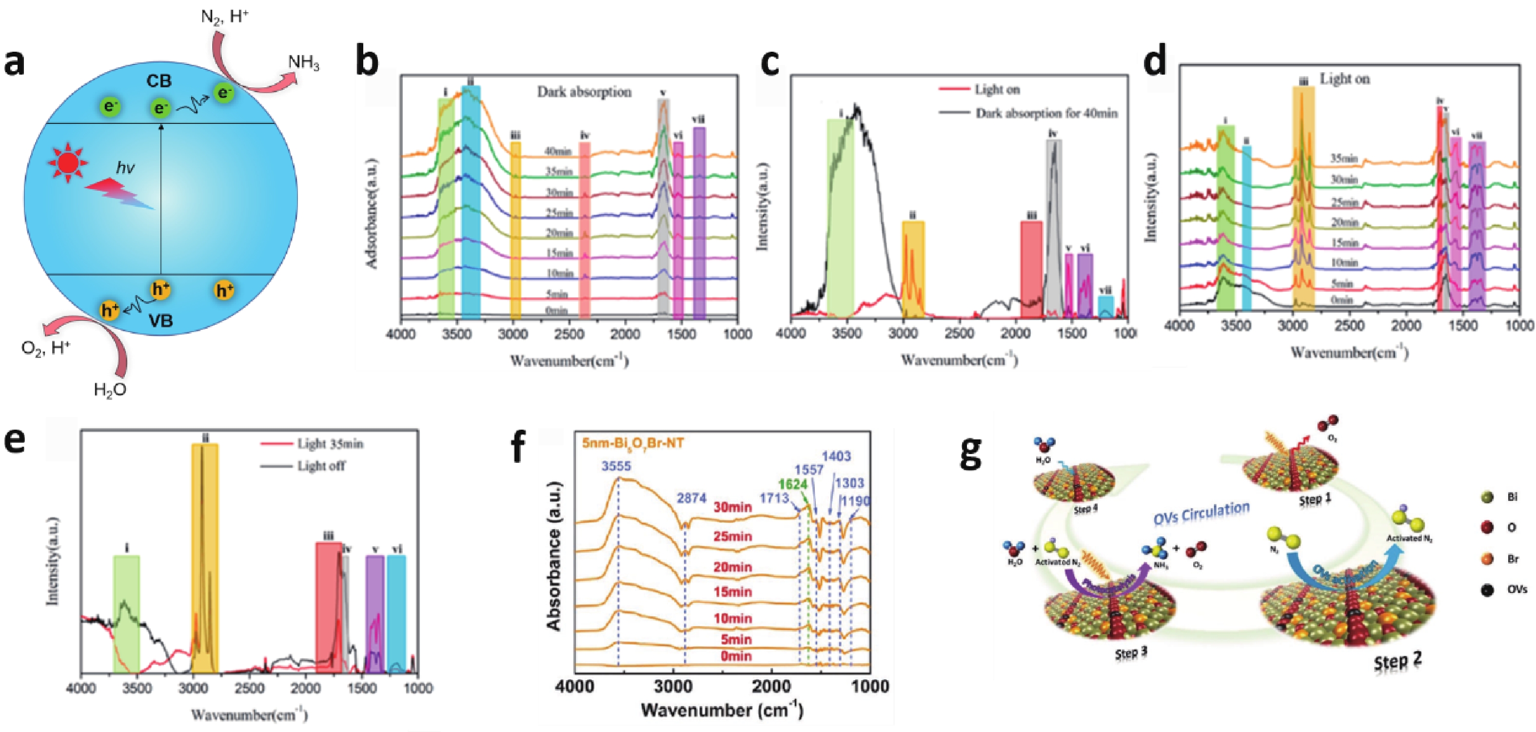
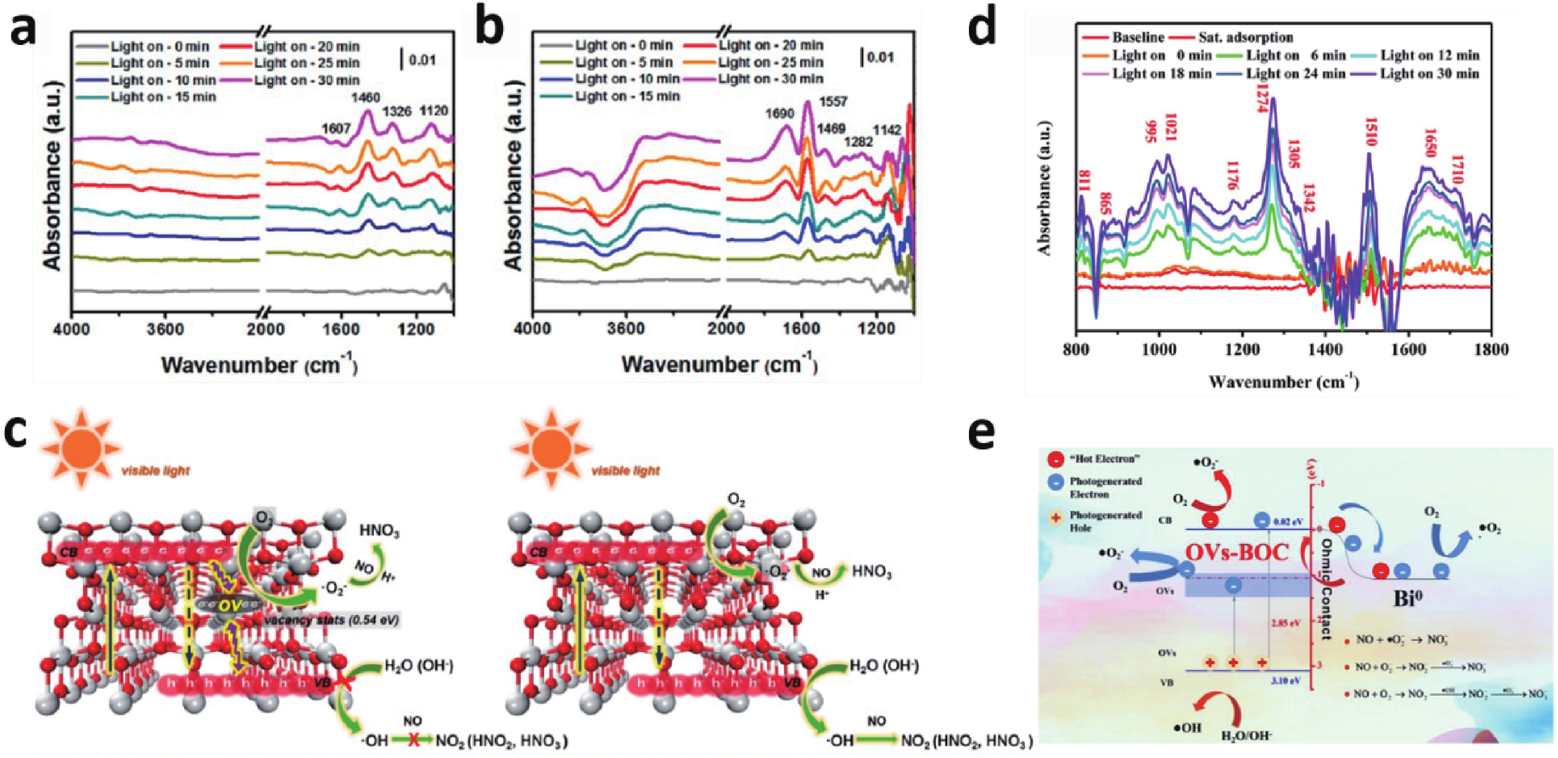
Semiconductor photocatalysis, as a key part of solar energy utilization, has far-reaching implications for industrial, agricultural, and commercial development. Lack of understanding of the catalyst evolution and the reaction mechanism is a critical obstacle for designing efficient and stable photocatalysts. This review summarizes the recent progress of in-situ exploring the dynamic behavior of catalyst materials and reaction intermediates. Semiconductor photocatalytic processes and two major classes of in-situ techniques that include microscopic imaging and spectroscopic characterization are presented. Finally, problems and challenges in in-situ characterization are proposed, geared toward developing more advanced in-situ techniques and monitoring more accurate and realistic reaction processes, to guide designing advanced photocatalysts.


J. Semicond.
2022, 43(4): 041105 doi: 10.1088/1674-4926/43/4/041105
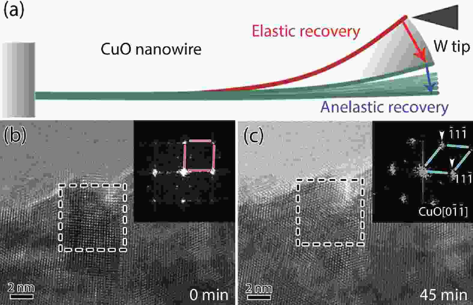
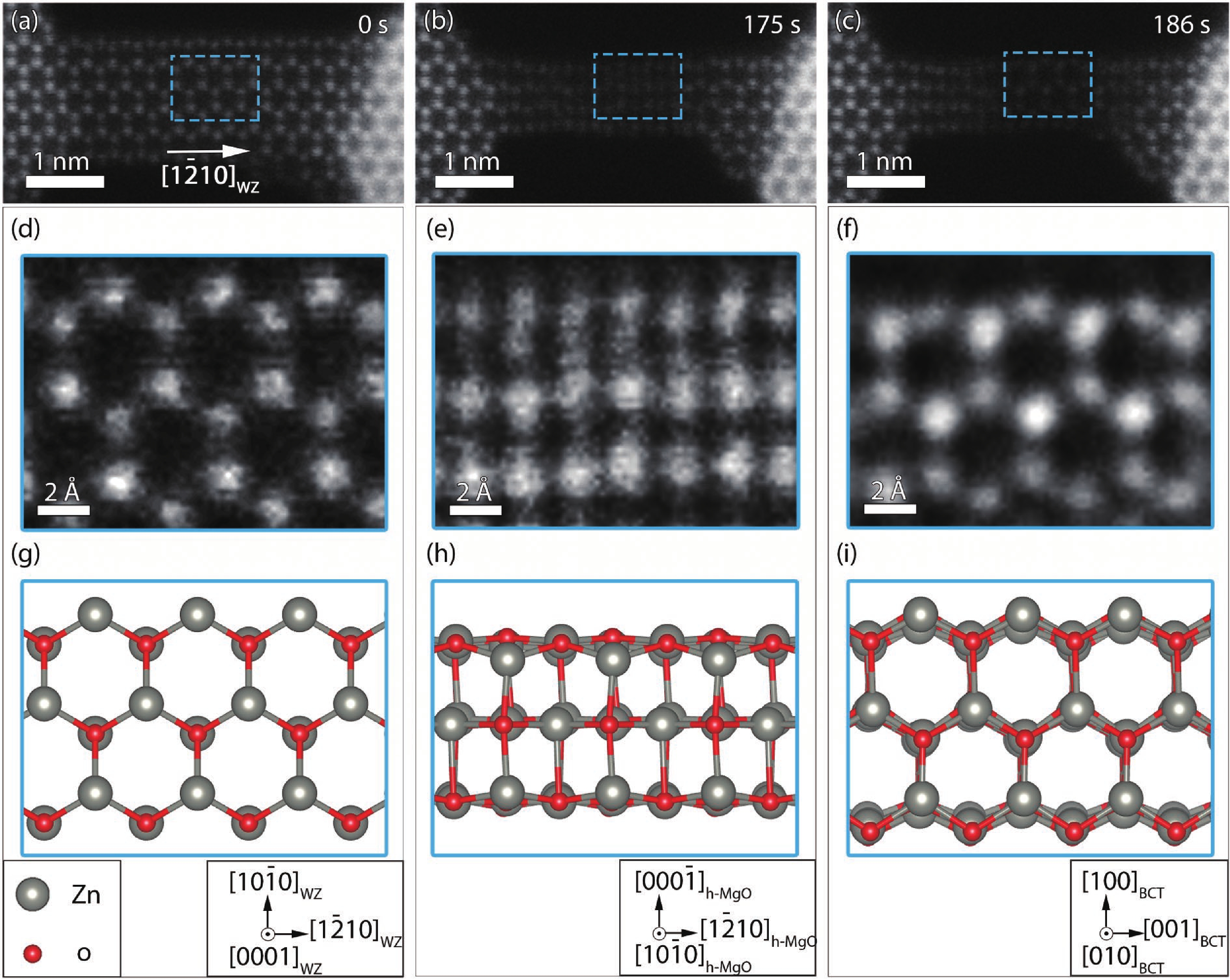
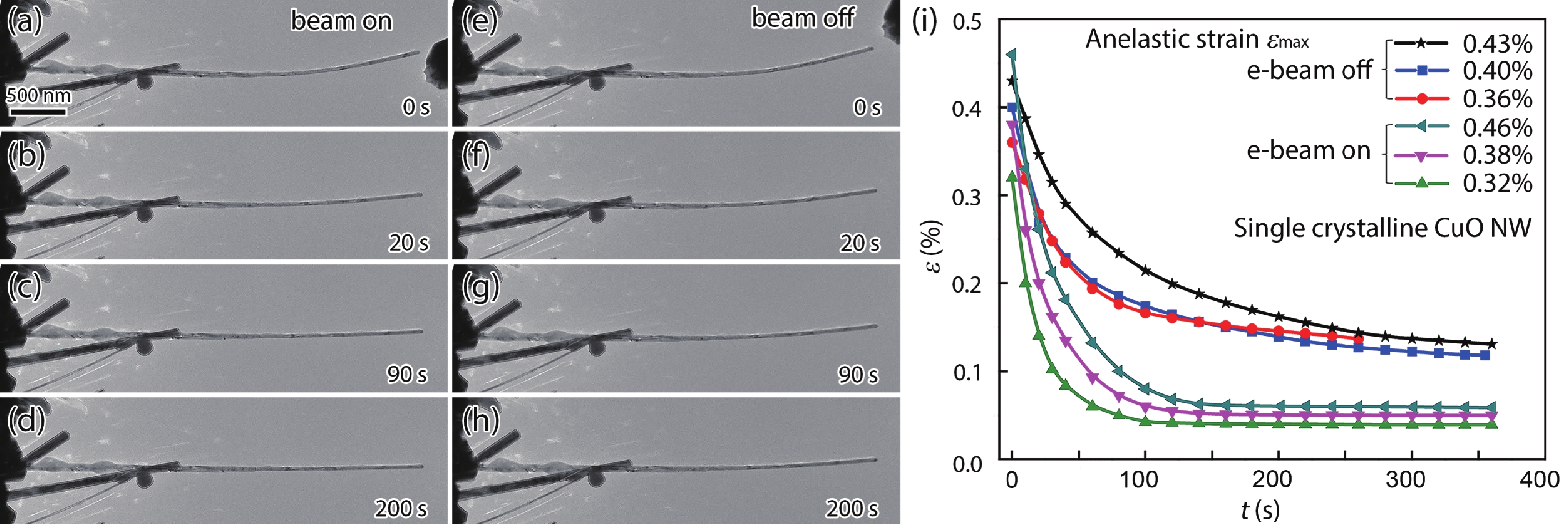
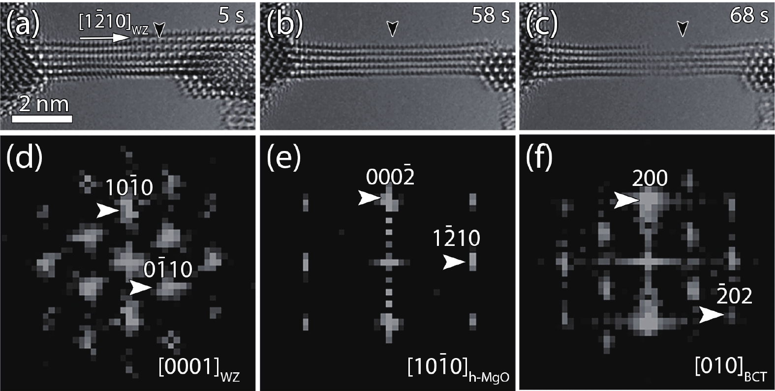
Metal oxide semiconductors (MOSs) are attractive candidates as functional parts and connections in nanodevices. Upon spatial dimensionality reduction, the ubiquitous strain encountered in physical reality may result in structural instability and thus degrade the performance of MOS. Hence, the basic insight into the structural evolutions of low-dimensional MOS is a prerequisite for extensive applications, which unfortunately remains largely unexplored. Herein, we review the recent progress regarding the mechanical deformation mechanisms in MOSs, such as CuO and ZnO nanowires (NWs). We report the phase transformation of CuO NWs resulting from oxygen vacancy migration under compressive stress and the tensile strain-induced phase transition in ZnO NWs. Moreover, the influence of electron beam irradiation on interpreting the mechanical behaviors is discussed.


J. Semicond.
2022, 43(4): 041106 doi: 10.1088/1674-4926/43/4/041106
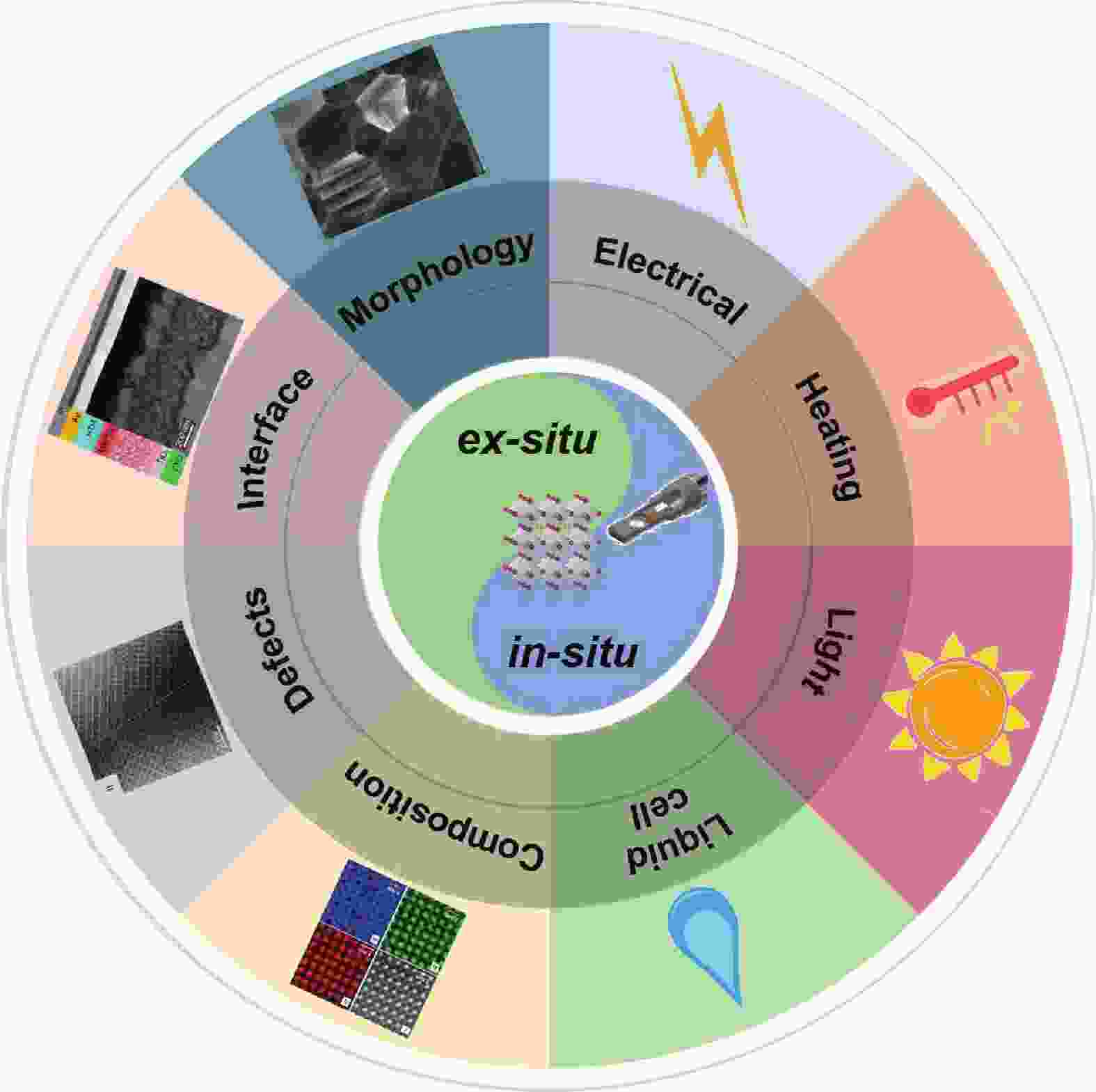
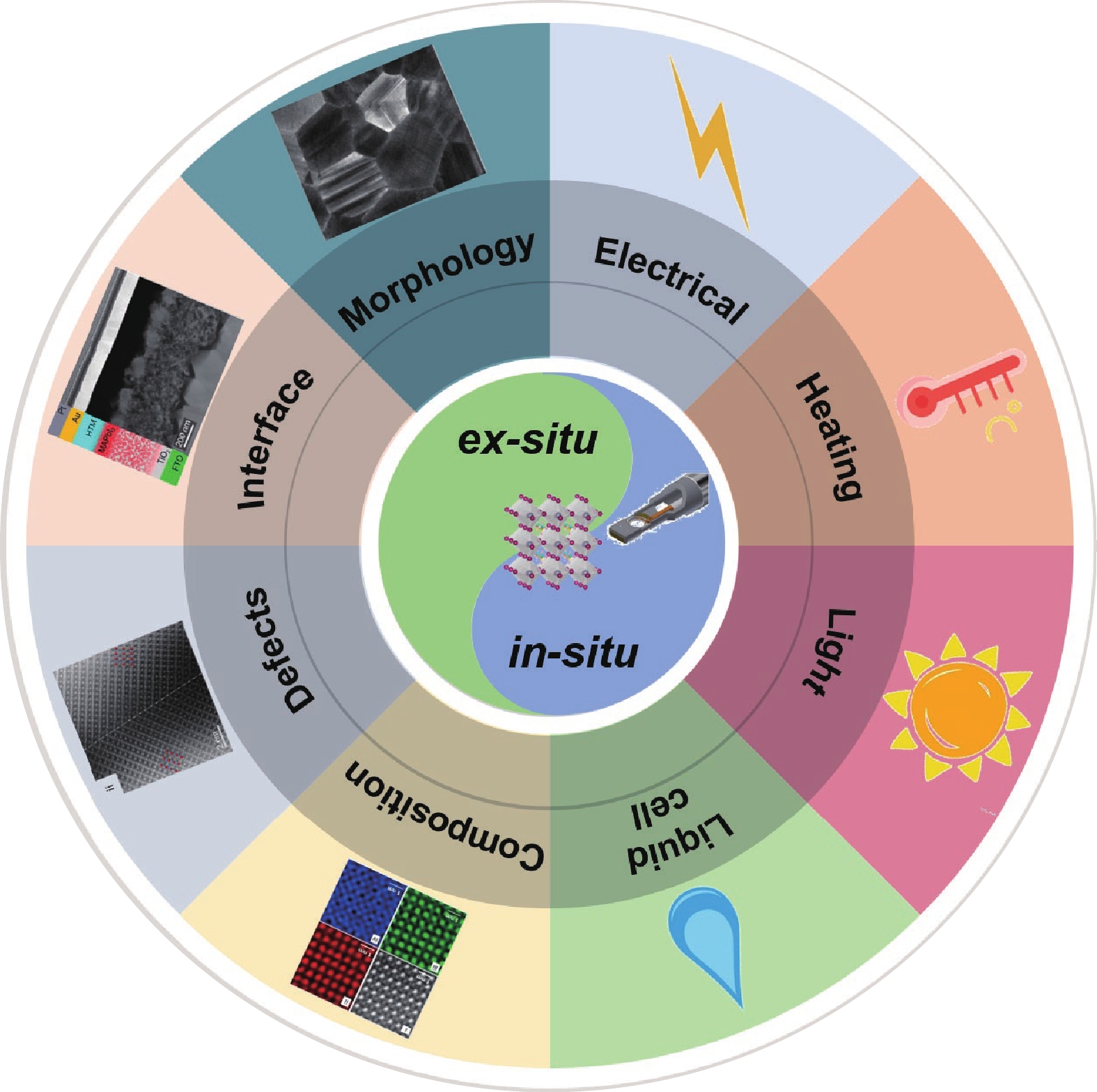
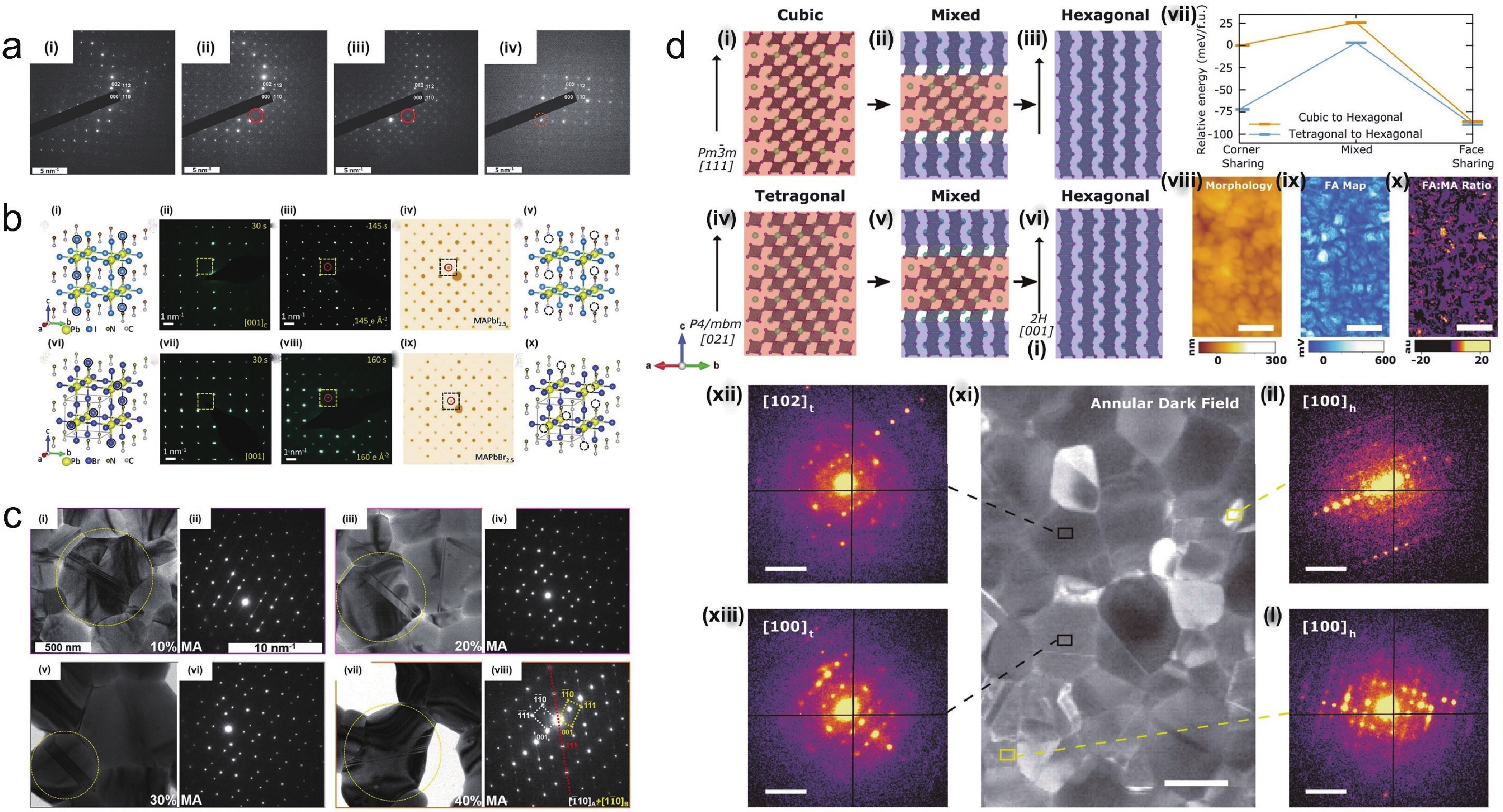
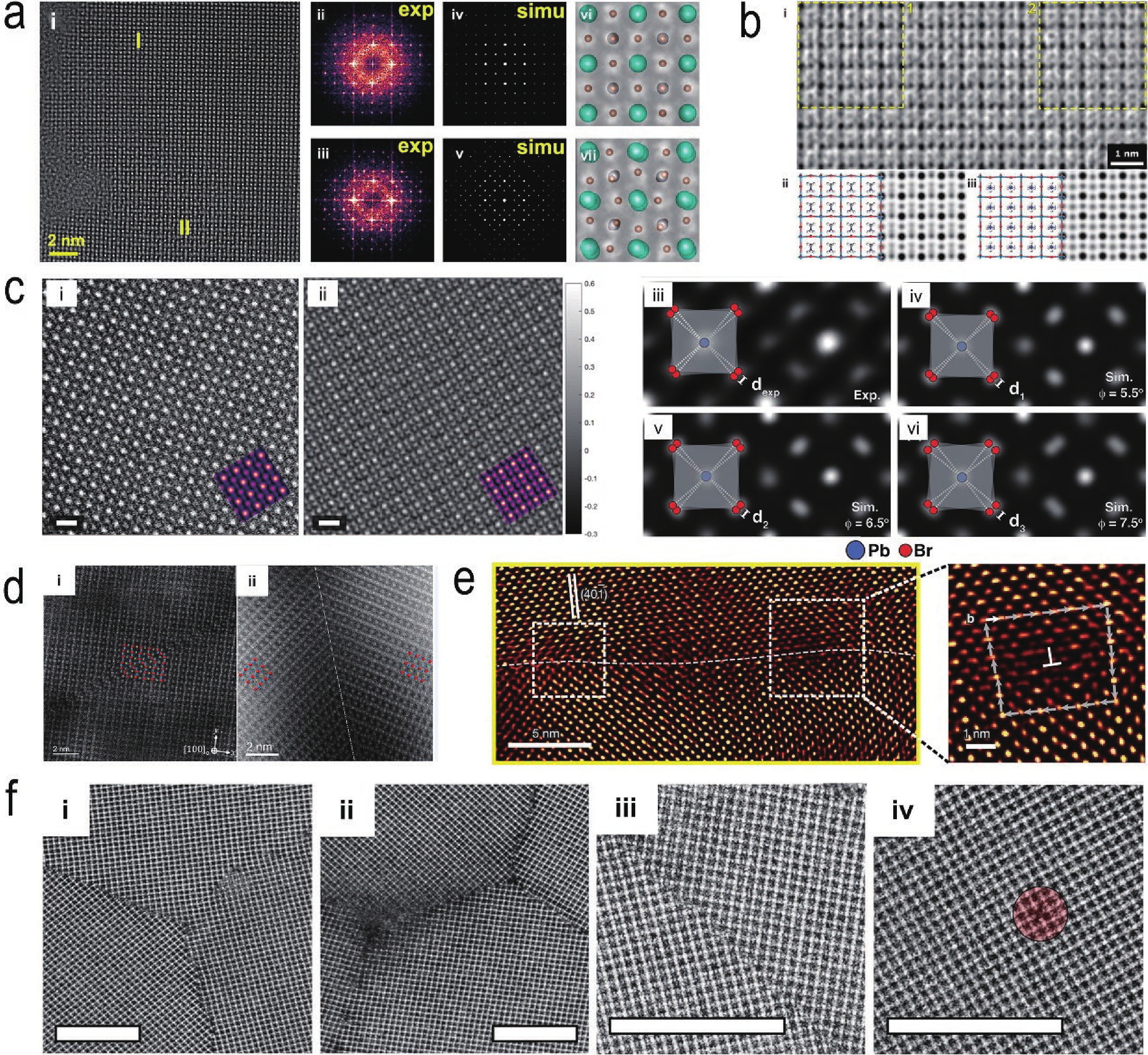
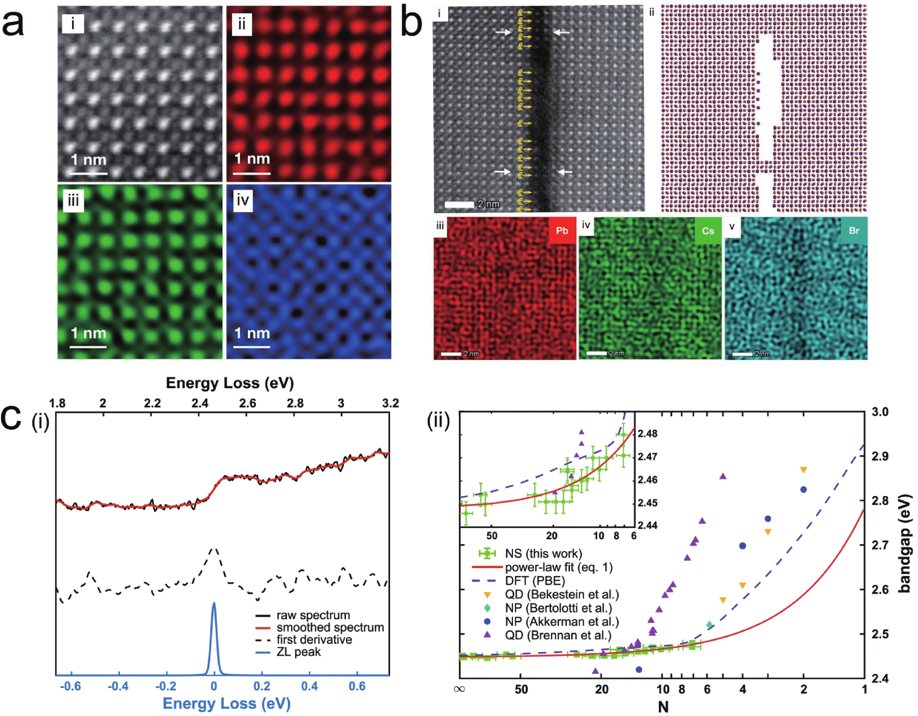
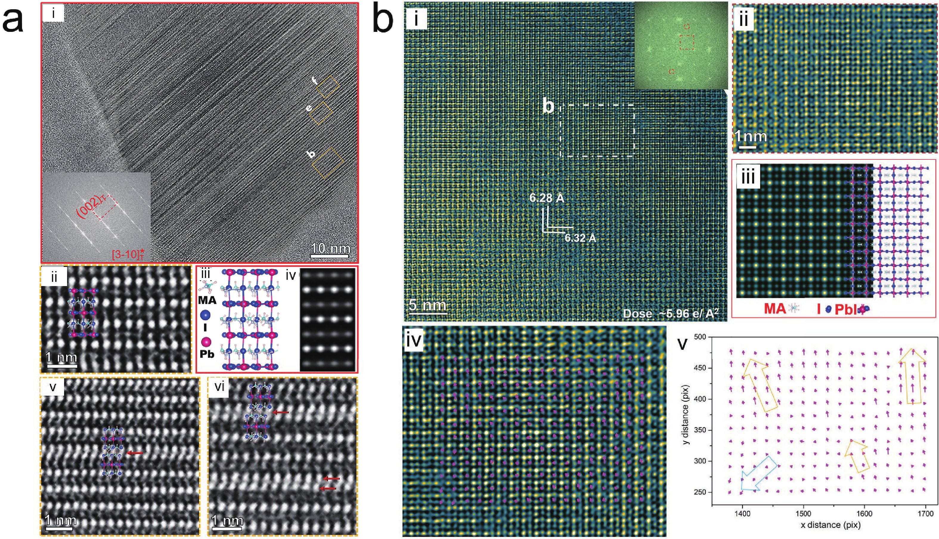
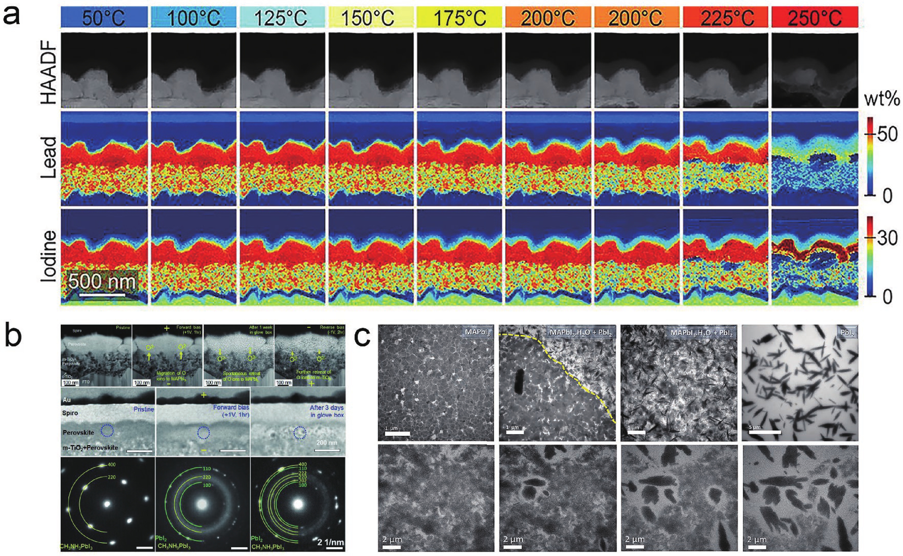
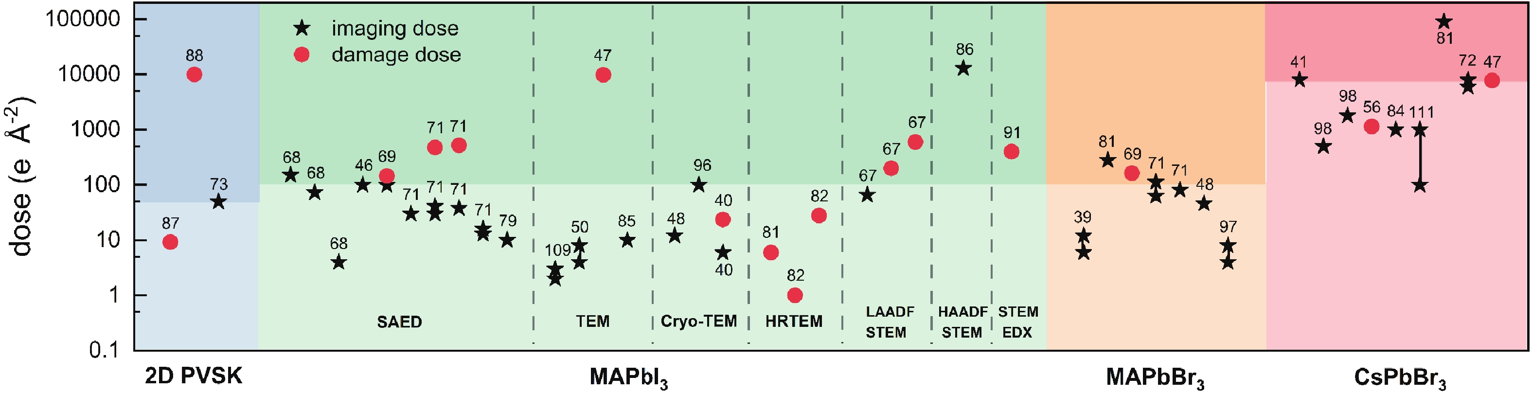
Halide perovskites are strategically important in the field of energy materials. Along with the rapid development of the materials and related devices, there is an urgent need to understand the structure–property relationship from nanoscale to atomic scale. Much effort has been made in the past few years to overcome the difficulty of imaging limited by electron dose, and to further extend the investigation towards operando conditions. This review is dedicated to recent studies of advanced transmission electron microscopy (TEM) characterizations for halide perovskites. The irradiation damage caused by the interaction of electron beams and perovskites under conventional imaging conditions are first summarized and discussed. Low-dose TEM is then discussed, including electron diffraction and emerging techniques for high-resolution TEM (HRTEM) imaging. Atomic-resolution imaging, defects identification and chemical mapping on halide perovskites are reviewed. Cryo-TEM for halide perovskites is discussed, since it can readily suppress irradiation damage and has been rapidly developed in the past few years. Finally, the applications of in-situ TEM in the degradation study of perovskites under environmental conditions such as heating, biasing, light illumination and humidity are reviewed. More applications of emerging TEM characterizations are foreseen in the coming future, unveiling the structural origin of halide perovskite’s unique properties and degradation mechanism under operando conditions, so to assist the design of a more efficient and robust energy material.

J. Semicond.
2022, 43(4): 042101 doi: 10.1088/1674-4926/43/4/042101
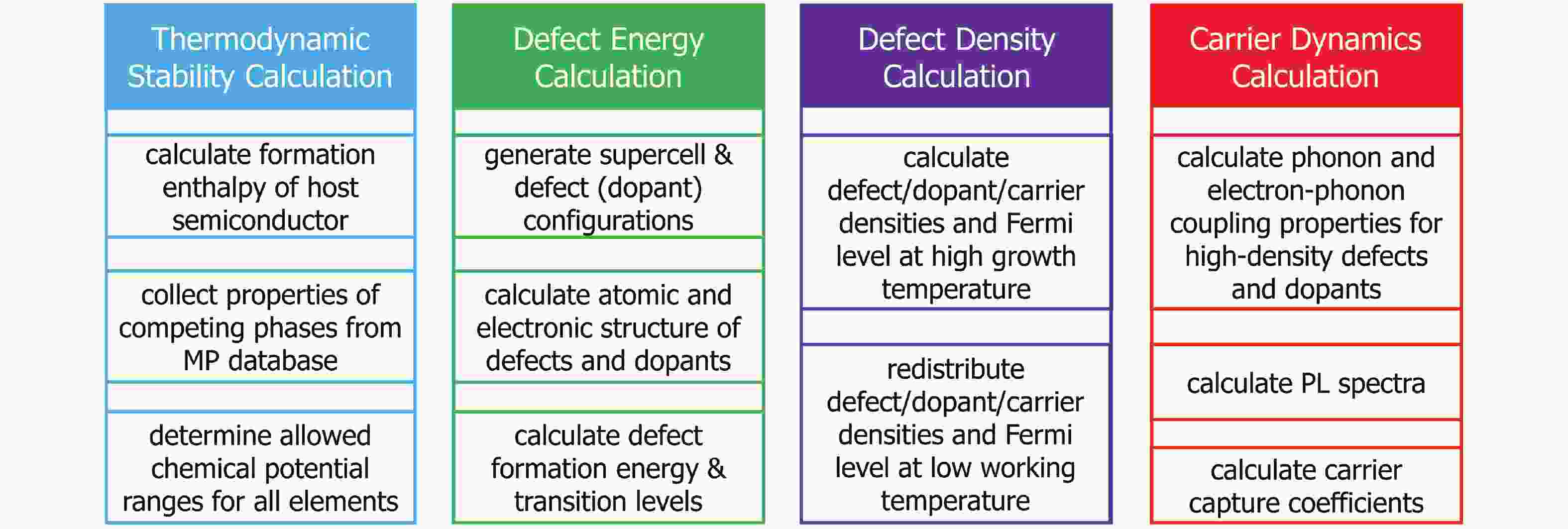
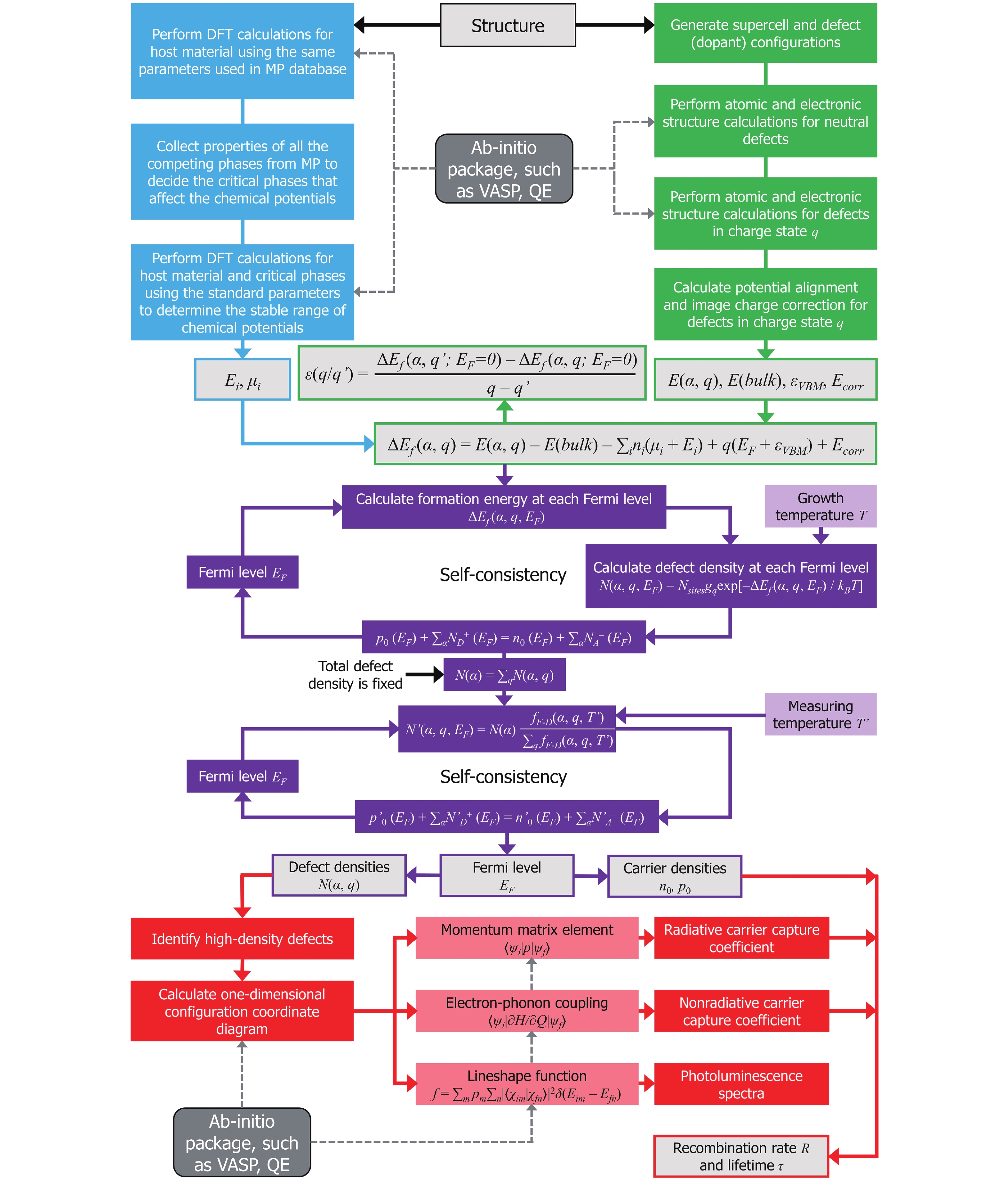
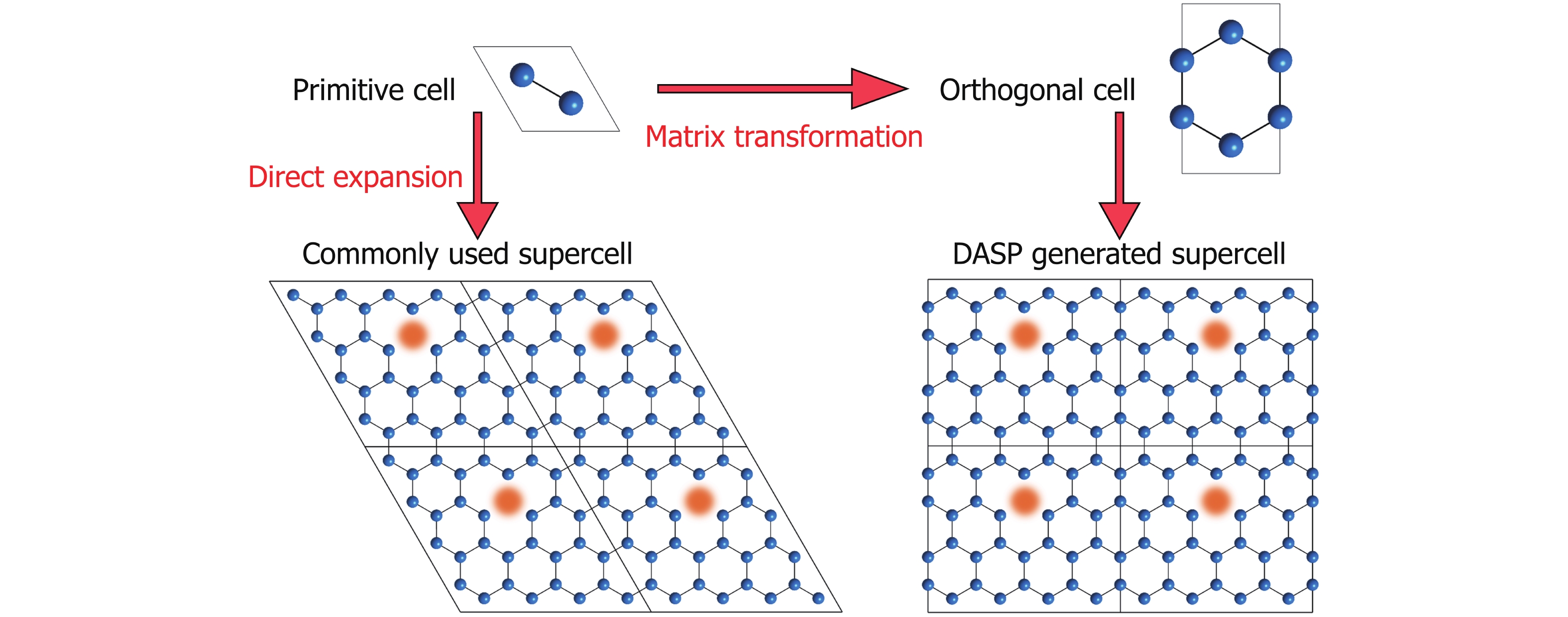
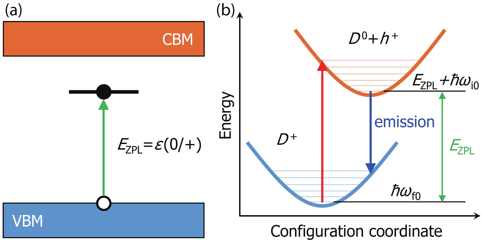
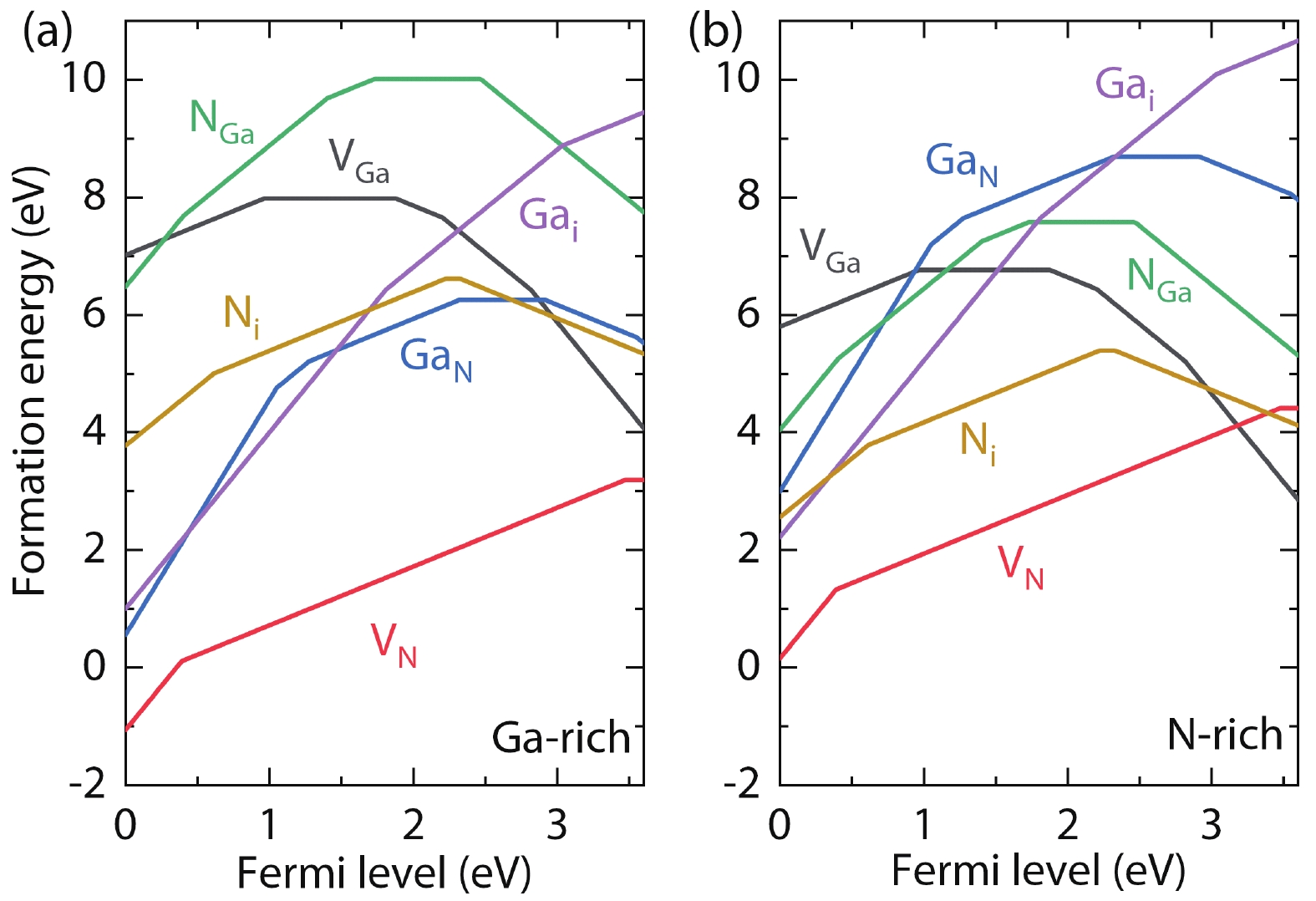
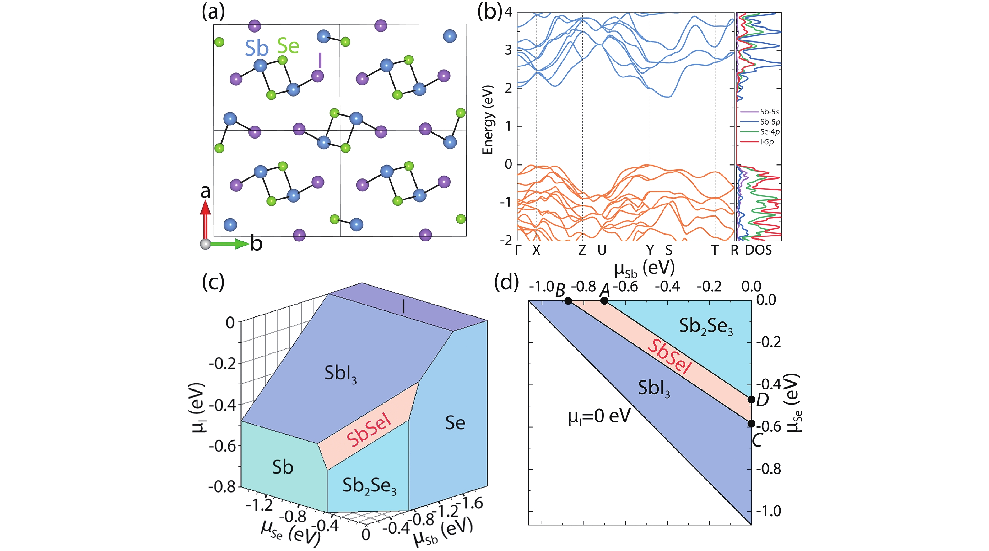
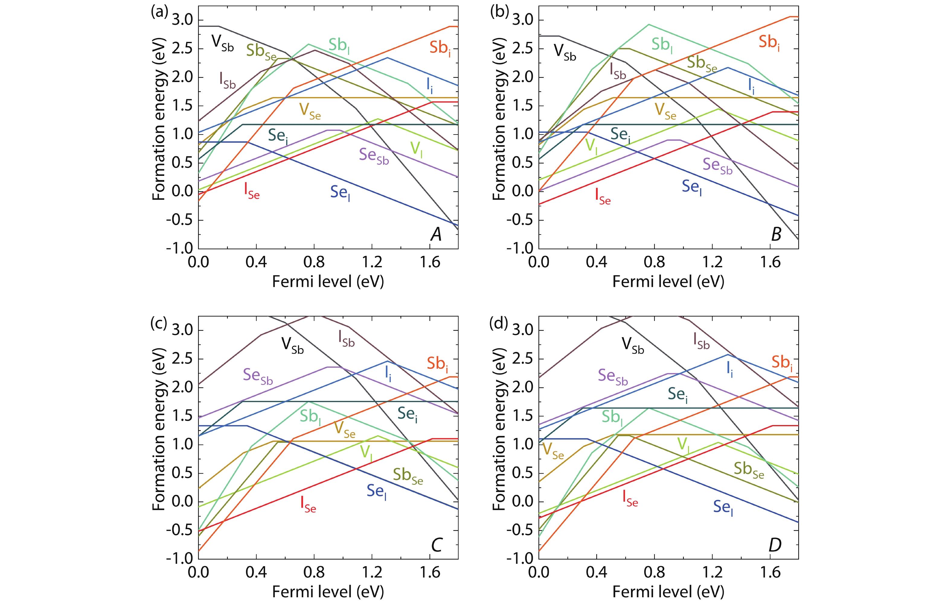
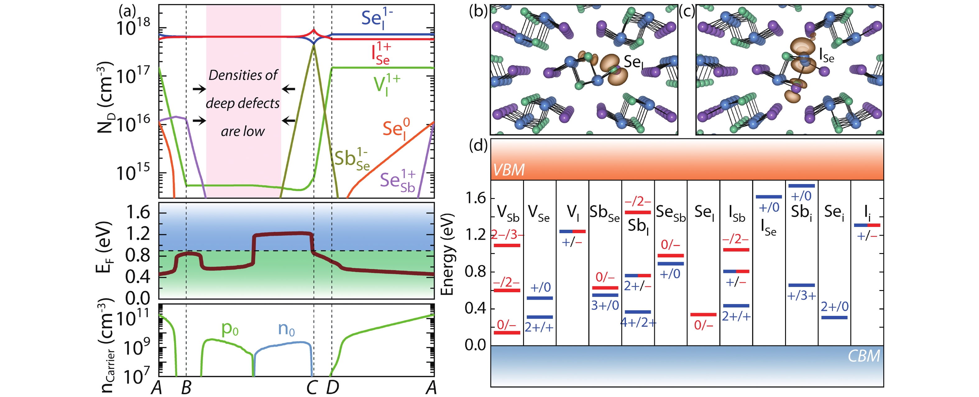
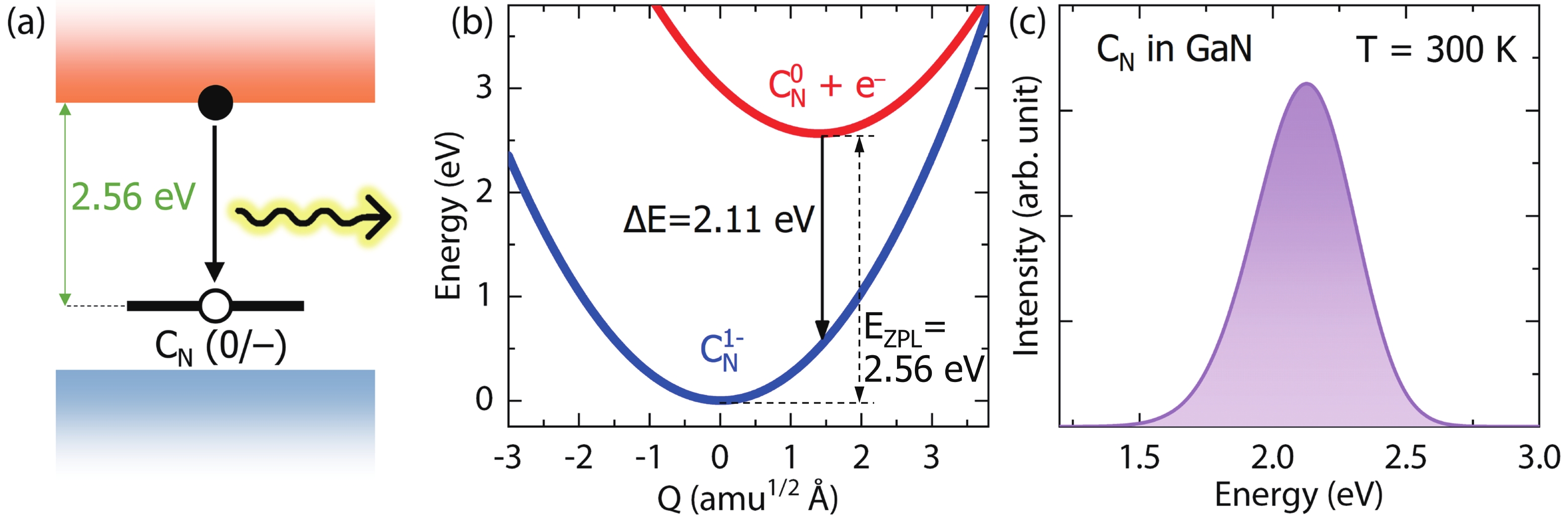
In order to perform automated calculations of defect and dopant properties in semiconductors and insulators, we developed a software package, the Defect and Dopant ab-initio Simulation Package (DASP), which is composed of four modules for calculating: (i) elemental chemical potentials, (ii) defect (dopant) formation energies and charge-state transition levels, (iii) defect and carrier densities and (iv) carrier dynamics properties of high-density defects. DASP uses the materials genome database for quick determination of competing secondary phases when calculating the elemental chemical potential that stabilizes compound semiconductors. DASP calls the ab-initio software to perform the total energy, structural relaxation and electronic structure calculations of the defect supercells with different charge states, based on which the defect formation energies and charge-state transition levels are calculated. Then DASP can calculate the equilibrium densities of defects and electron and hole carriers as well as the Fermi level in semiconductors under different chemical potential conditions and growth/working temperature. For high-density defects, DASP can calculate the carrier dynamics properties such as the photoluminescence (PL) spectrum and carrier capture cross sections which can interpret the deep level transient spectroscopy (DLTS). Here we will show three application examples of DASP in studying the undoped GaN, C-doped GaN and quasi-one-dimensional SbSeI.


J. Semicond.
2022, 43(4): 042501 doi: 10.1088/1674-4926/43/4/042501
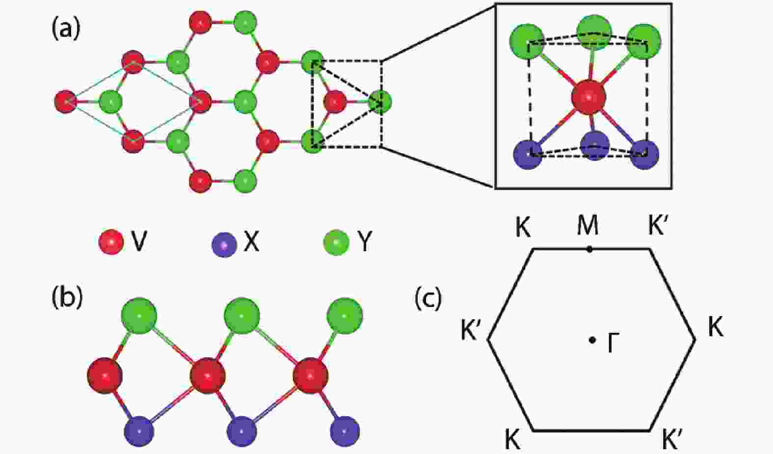
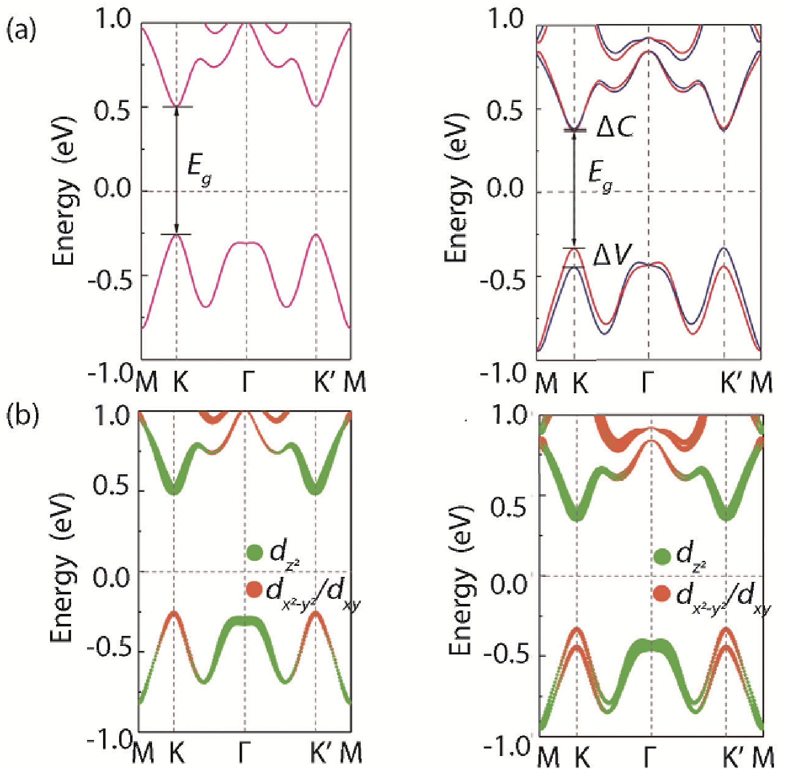
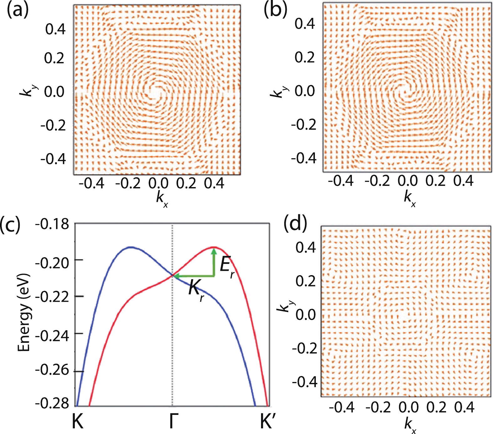
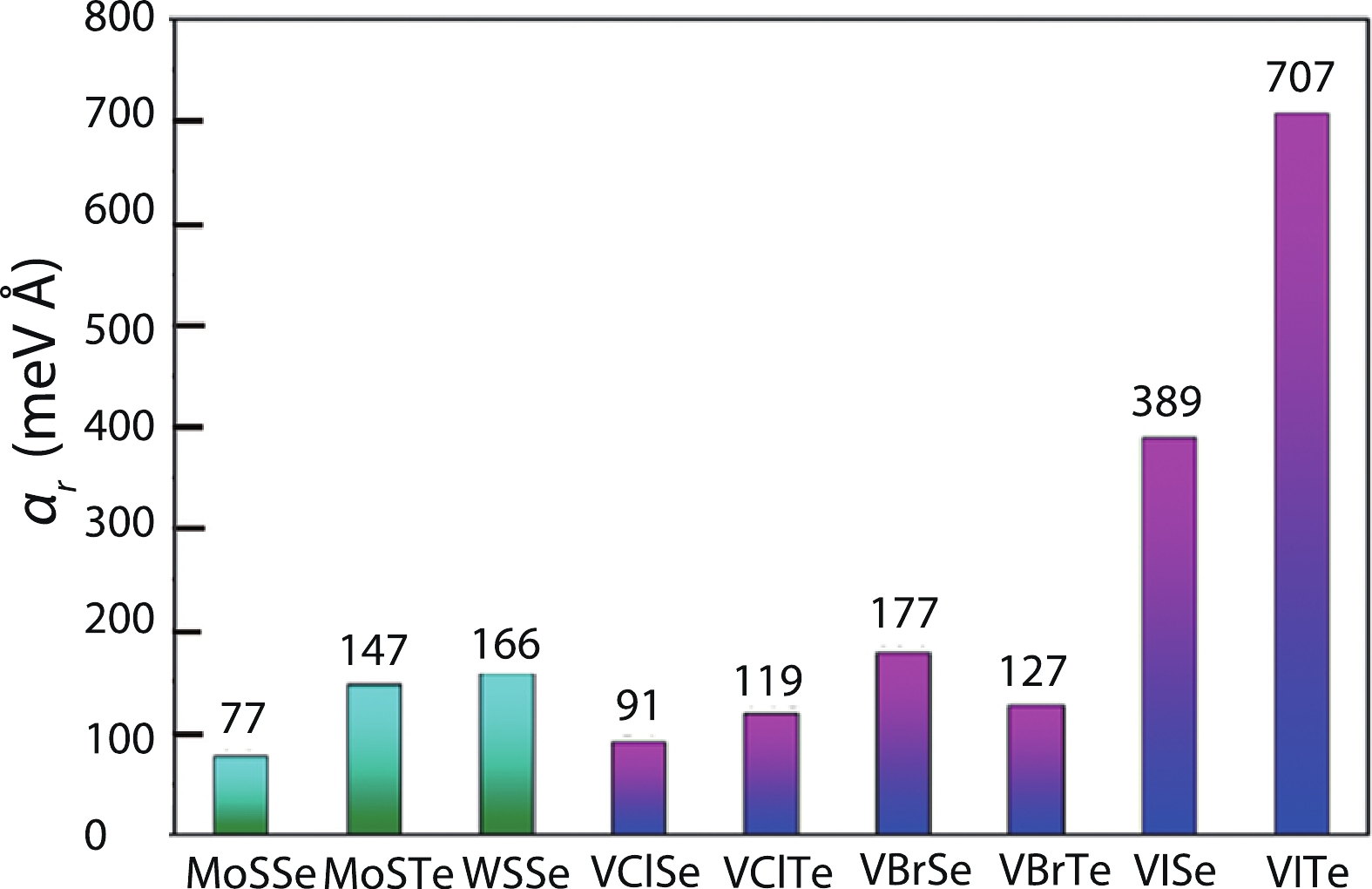
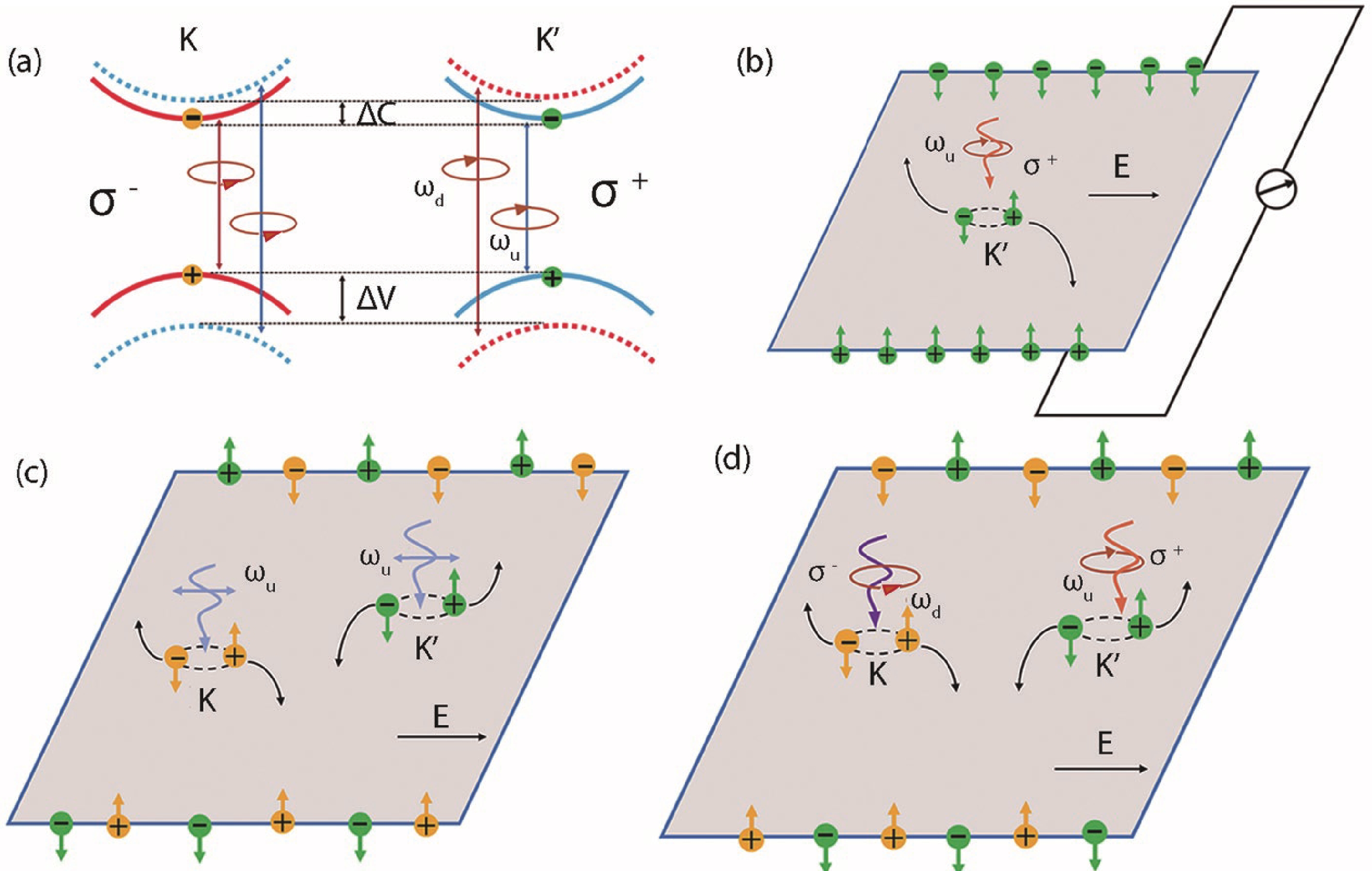
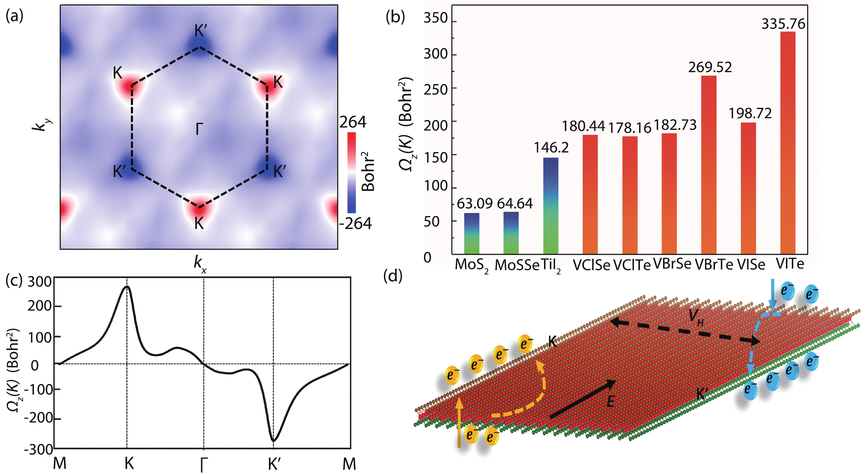
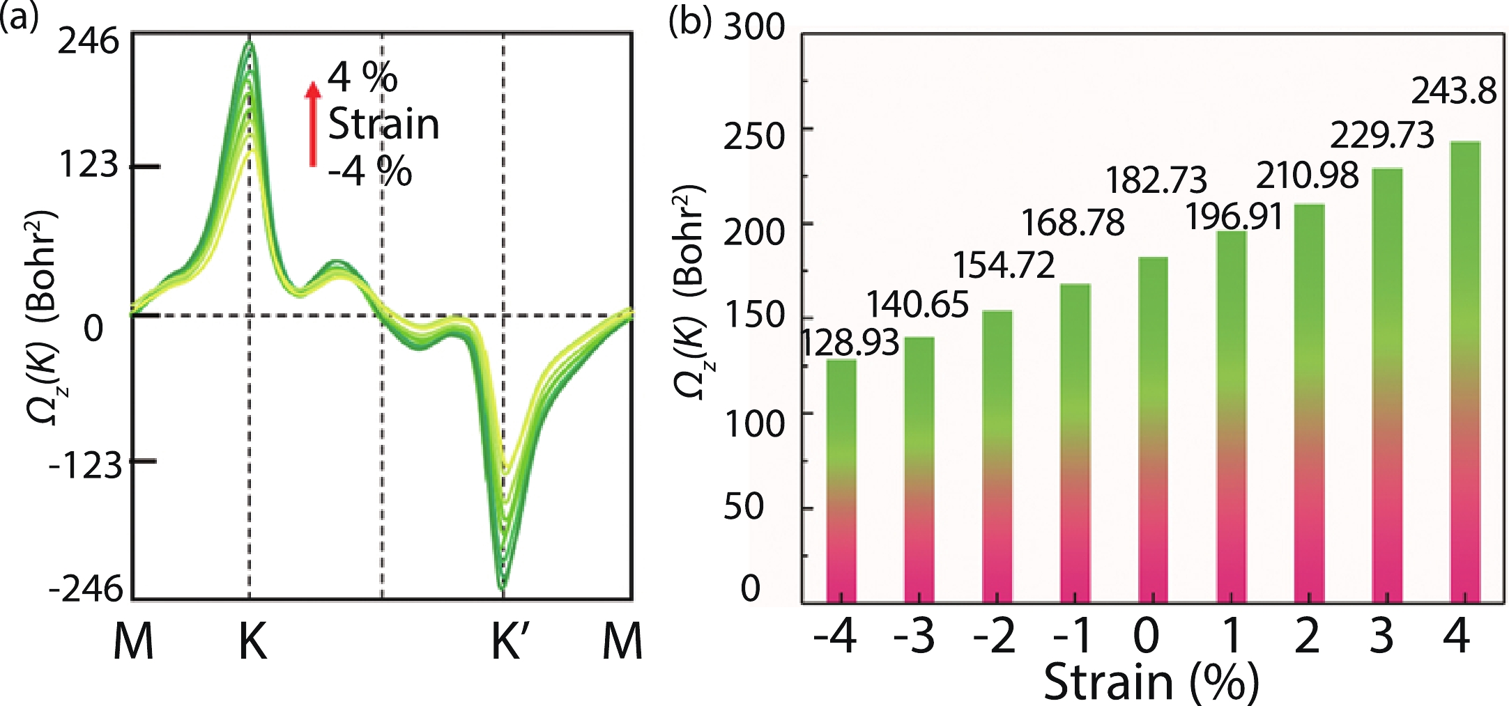
The Rashba effect and valley polarization provide a novel paradigm in quantum information technology. However, practical materials are scarce. Here, we found a new class of Janus monolayers VXY (X = Cl, Br, I; Y = Se, Te) with excellent valley polarization effect. In particular, Janus VBrSe shows Zeeman type spin splitting of 14 meV, large Berry curvature of 182.73 bohr2, and, at the same time, a large Rashba parameter of 176.89 meV·Å. We use the k·p theory to analyze the relationship between the lattice constant and the curvature of the Berry. The Berry curvature can be adjusted by changing the lattice parameter, which will greatly improve the transverse velocities of carriers and promote the efficiency of the valley Hall device. By applying biaxial strain onto VBrSe, we can see that there is a correlation between Berry curvature and lattice constant, which further validates the above theory. All these results provide tantalizing opportunities for efficient spintronics and valleytronics.