


Issue Browser
Volume 42, Issue 12,
Dec 2021


J. Semicond.
2021, 42(12): 122001 doi: 10.1088/1674-4926/42/12/122001
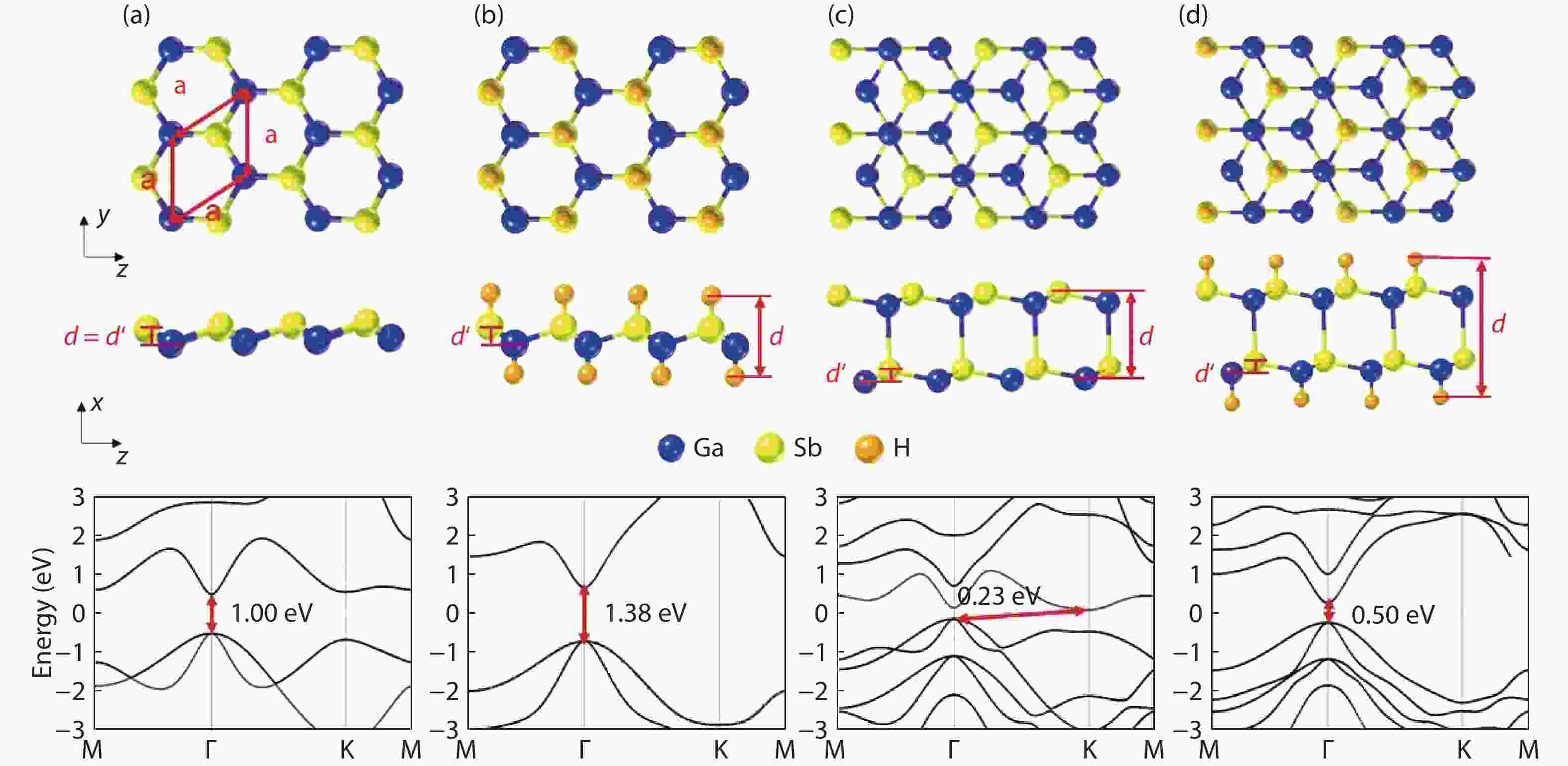
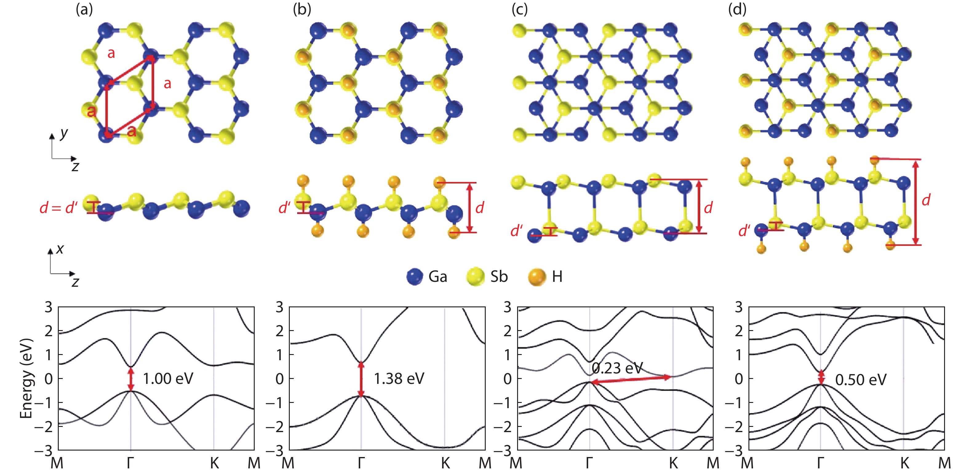
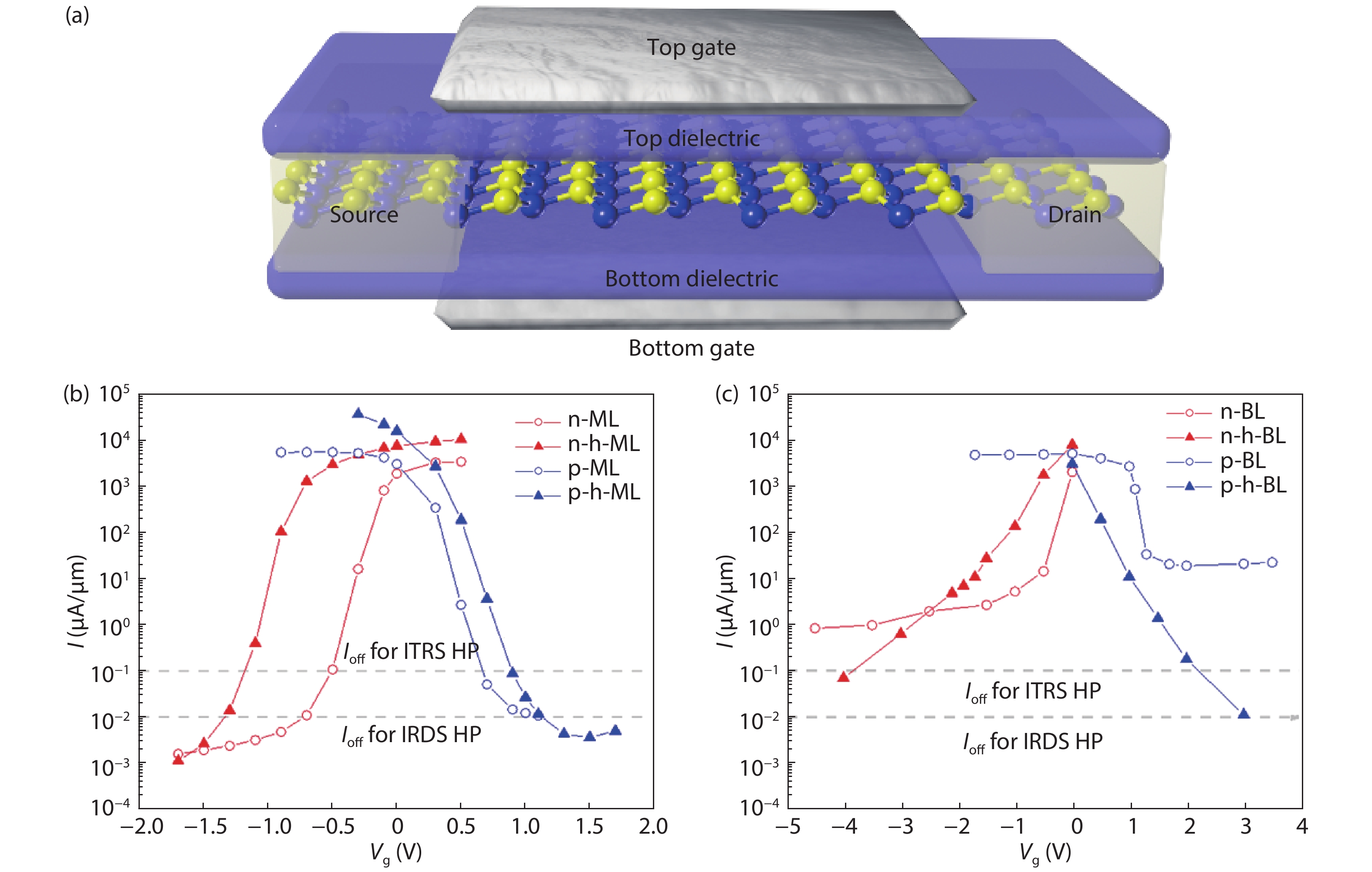
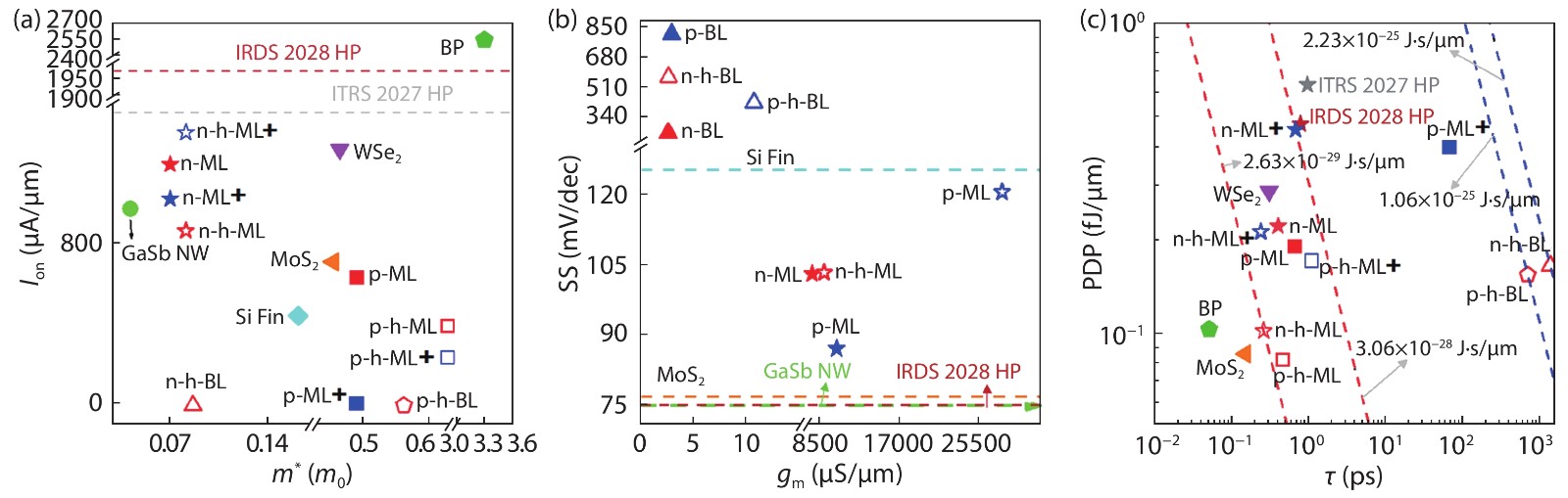
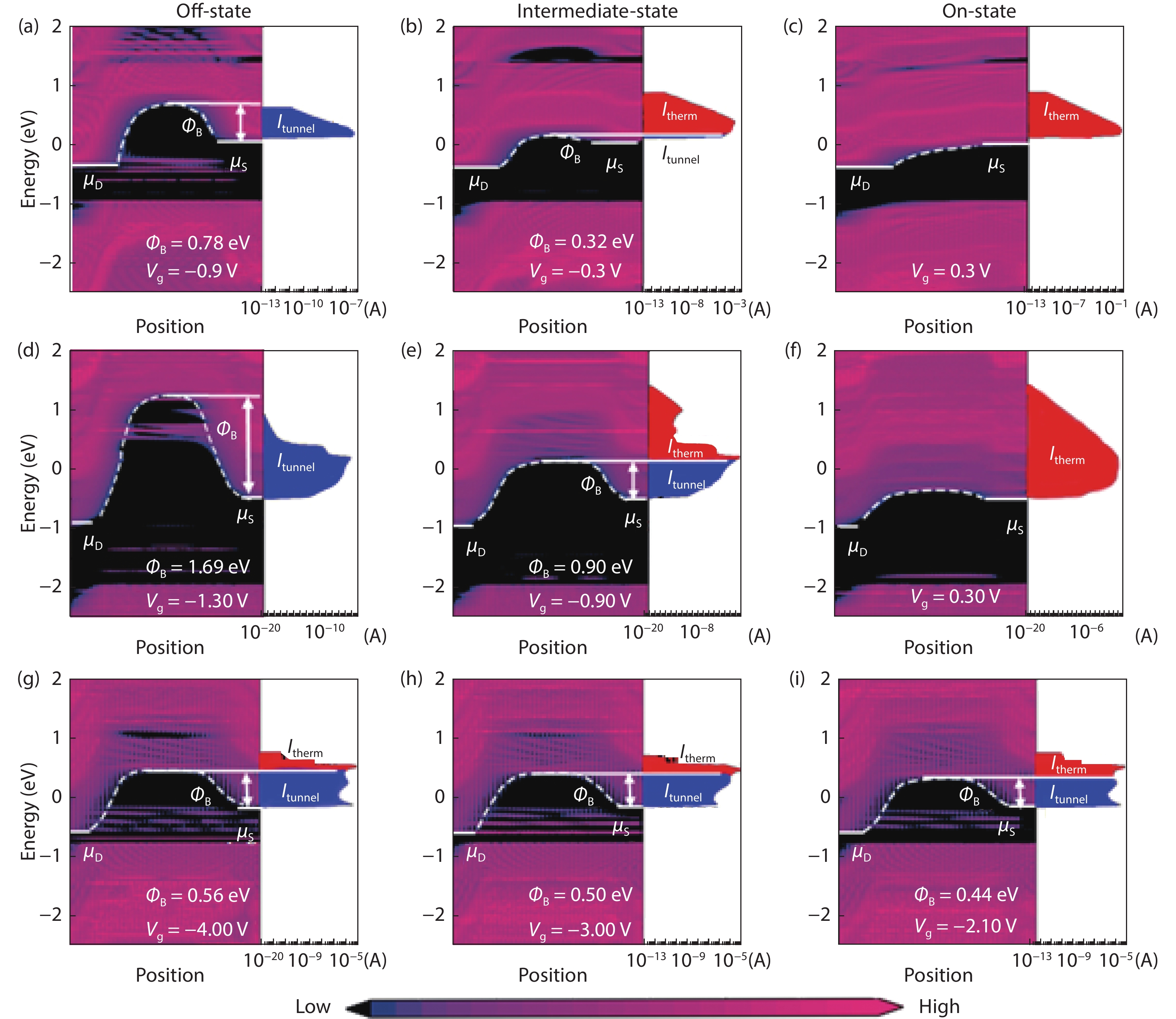
Owing to the high carrier mobility, two-dimensional (2D) gallium antimonite (GaSb) is a promising channel material for field-effect transistors (FETs) in the post-silicon era. We investigated the ballistic performance of the 2D GaSb metal–oxide–semiconductor FETs with a 10 nm-gate-length by the ab initio quantum transport simulation. Because of the wider bandgap and better gate-control ability, the performance of the 10-nm monolayer (ML) GaSb FETs is generally superior to the bilayer counterparts, including the three-to-four orders of magnitude larger on-current. Via hydrogenation, the delay-time and power consumption can be further enhanced with magnitude up to 35% and 57%, respectively, thanks to the expanded bandgap. The 10-nm ML GaSb FETs can almost meet the International Technology Roadmap for Semiconductors (ITRS) for high-performance demands in terms of the on-state current, intrinsic delay time, and power-delay product.
J. Semicond.
2021, 42(12): 122002 doi: 10.1088/1674-4926/42/12/122002
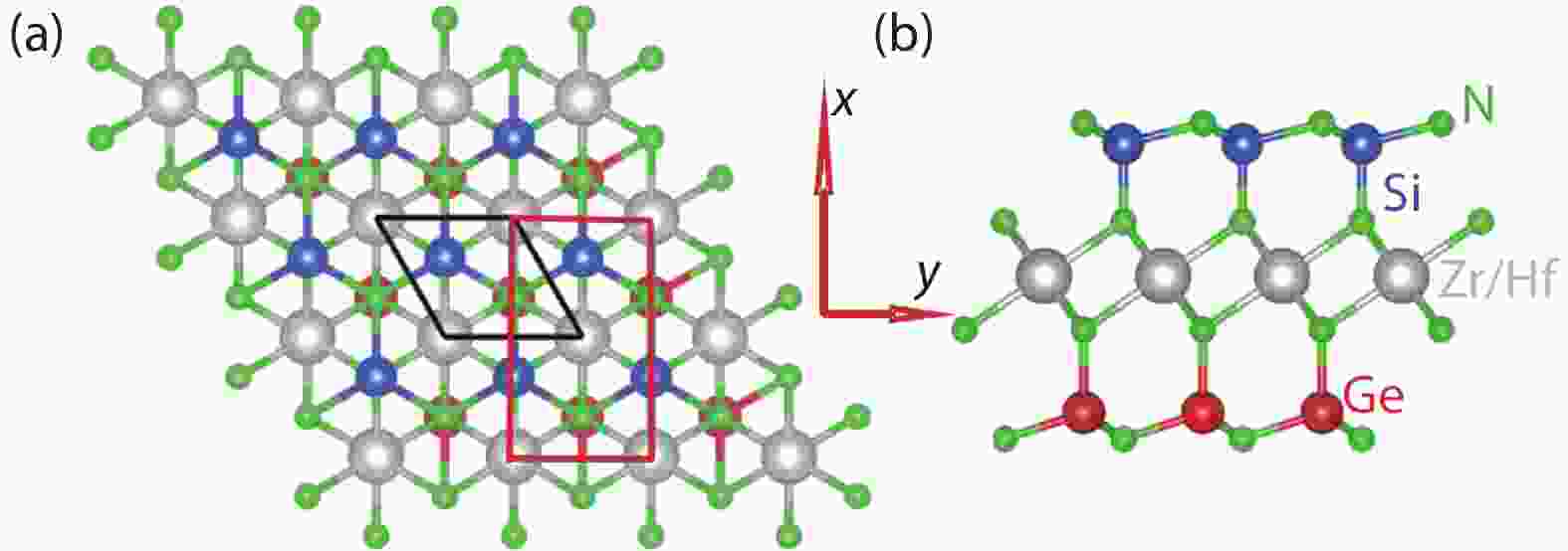
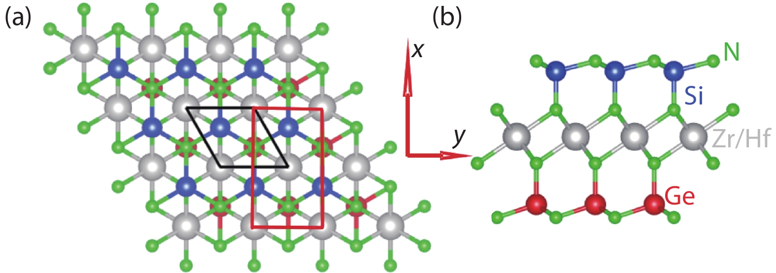
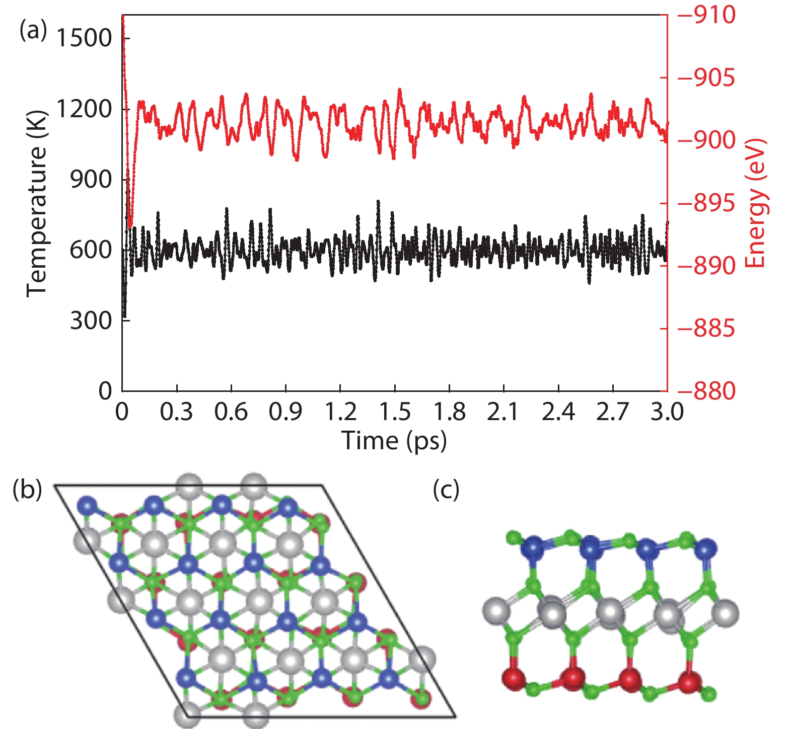
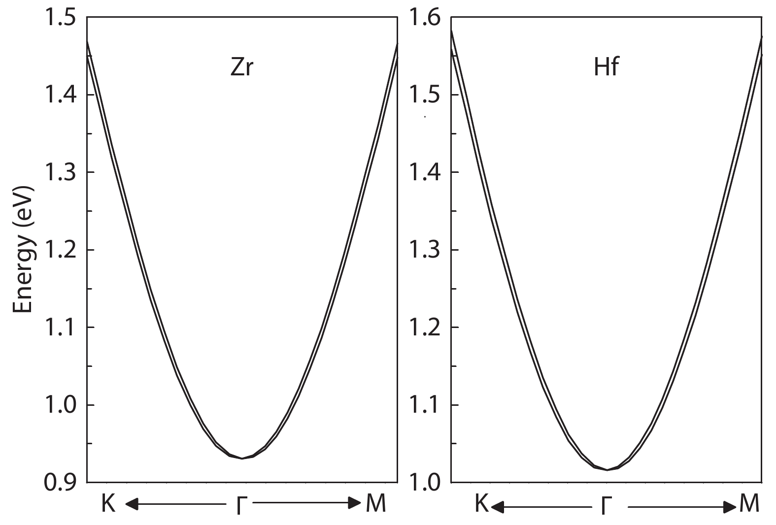
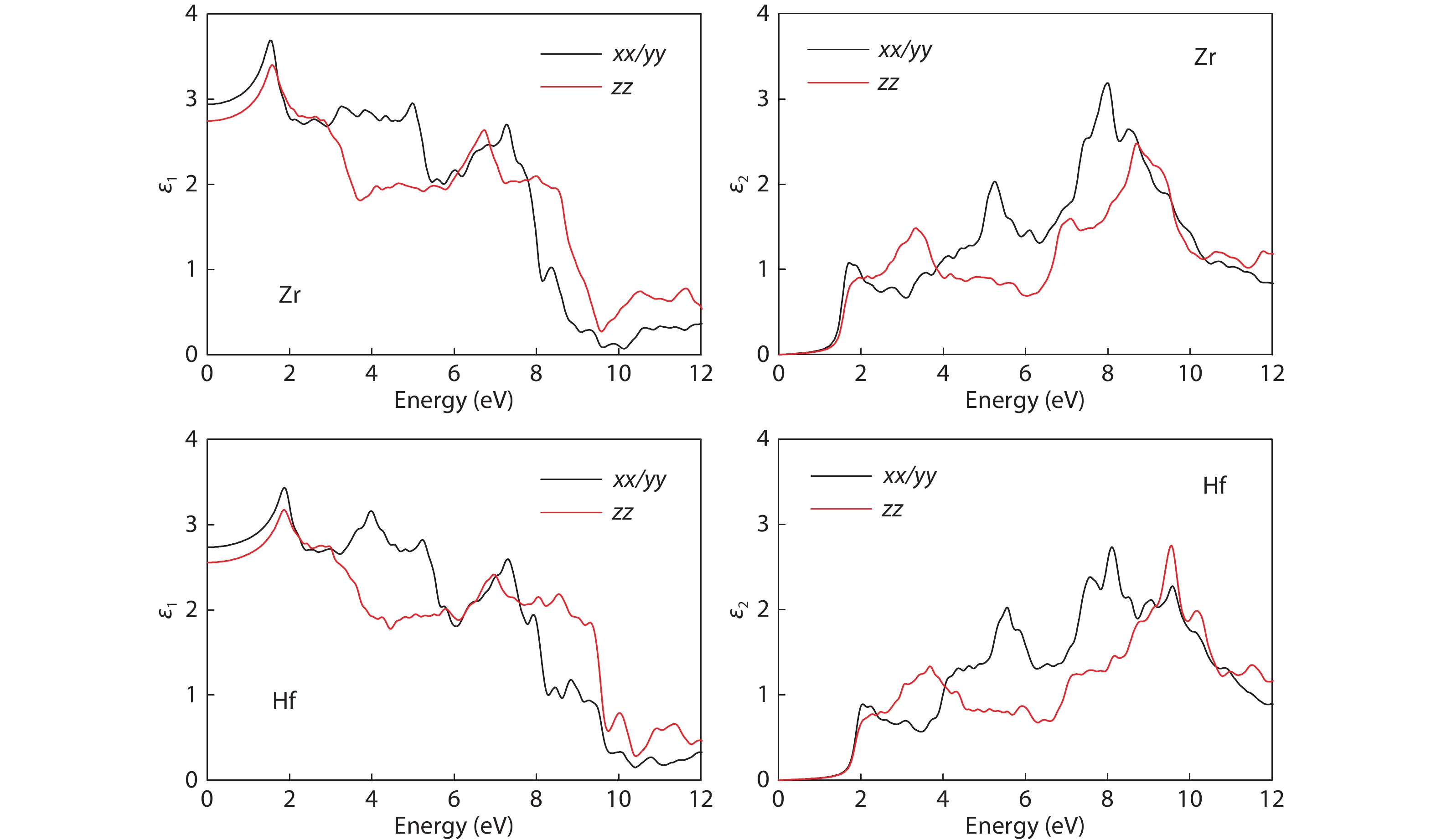
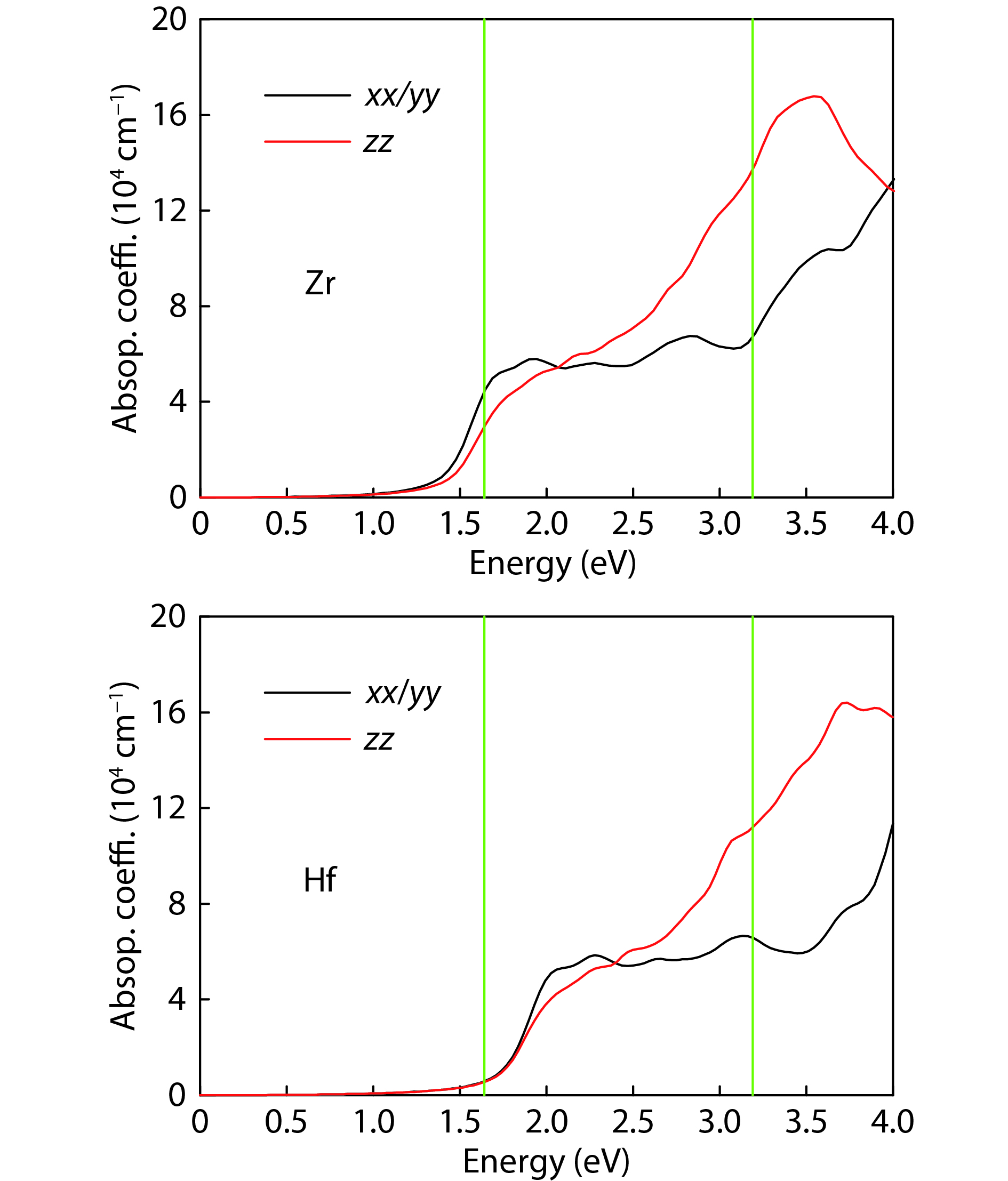
A two-dimensional (2D) MA2Z4 family with


J. Semicond.
2021, 42(12): 122701 doi: 10.1088/1674-4926/42/12/122701

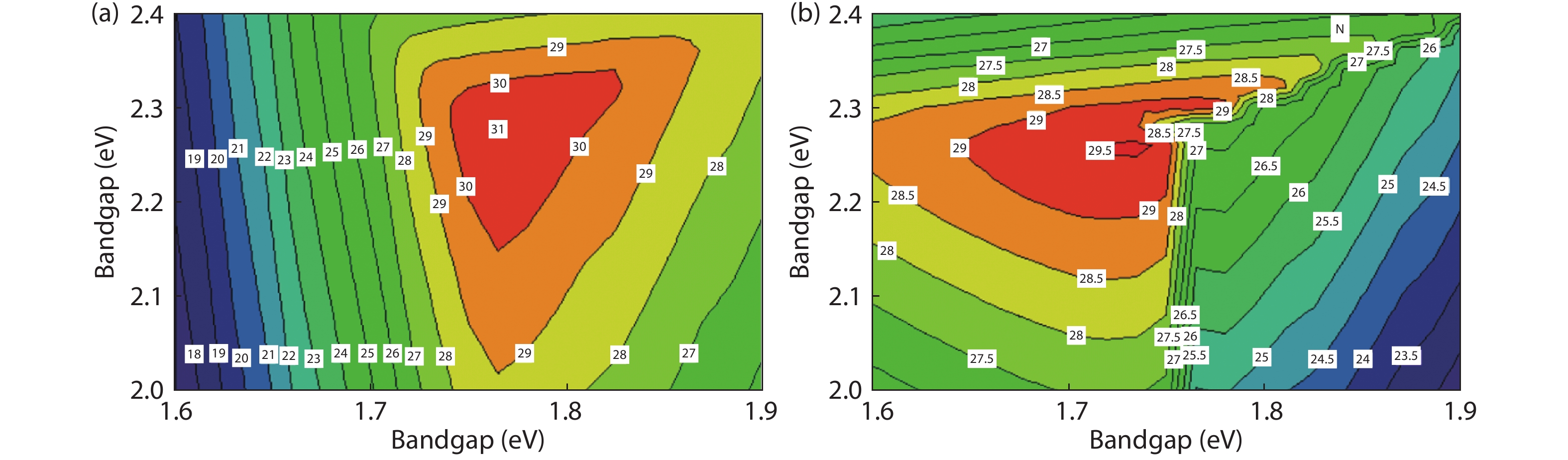
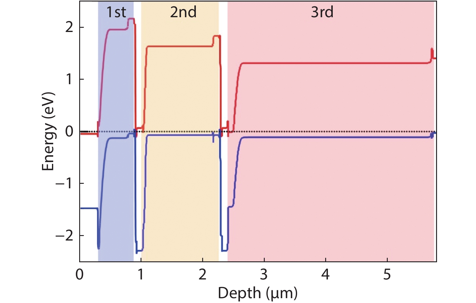
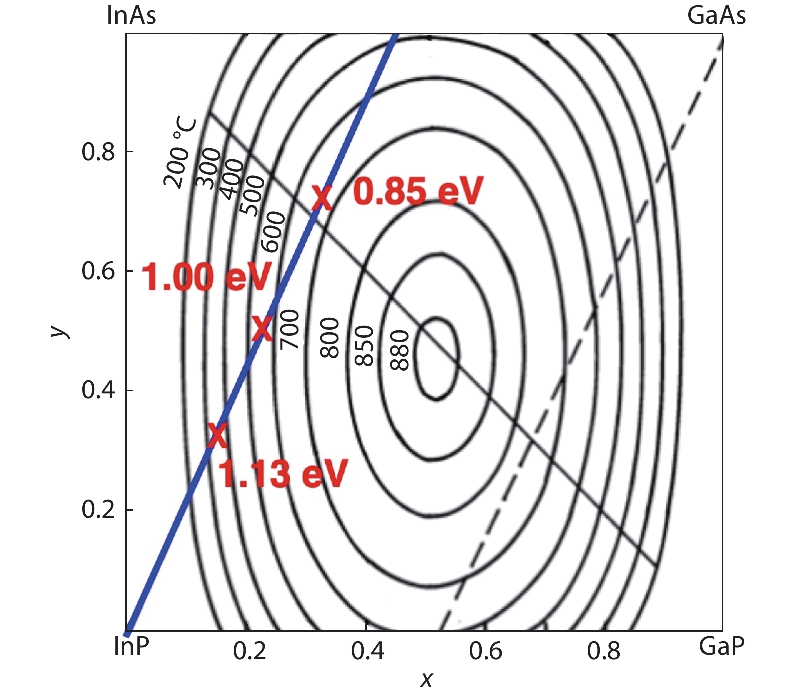
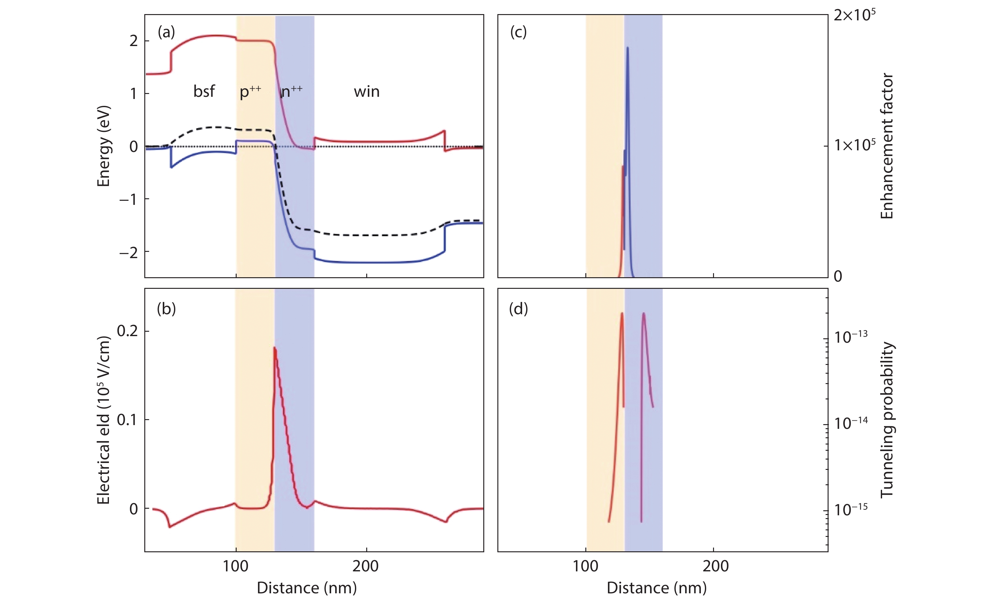
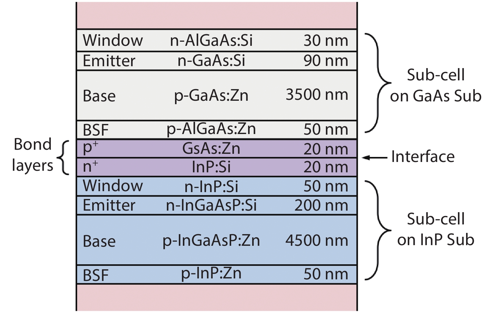
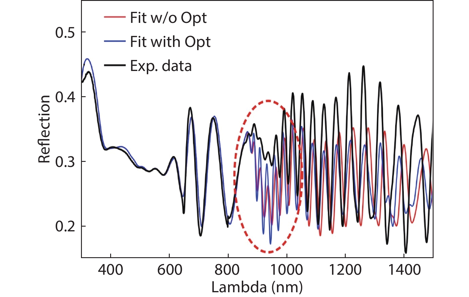
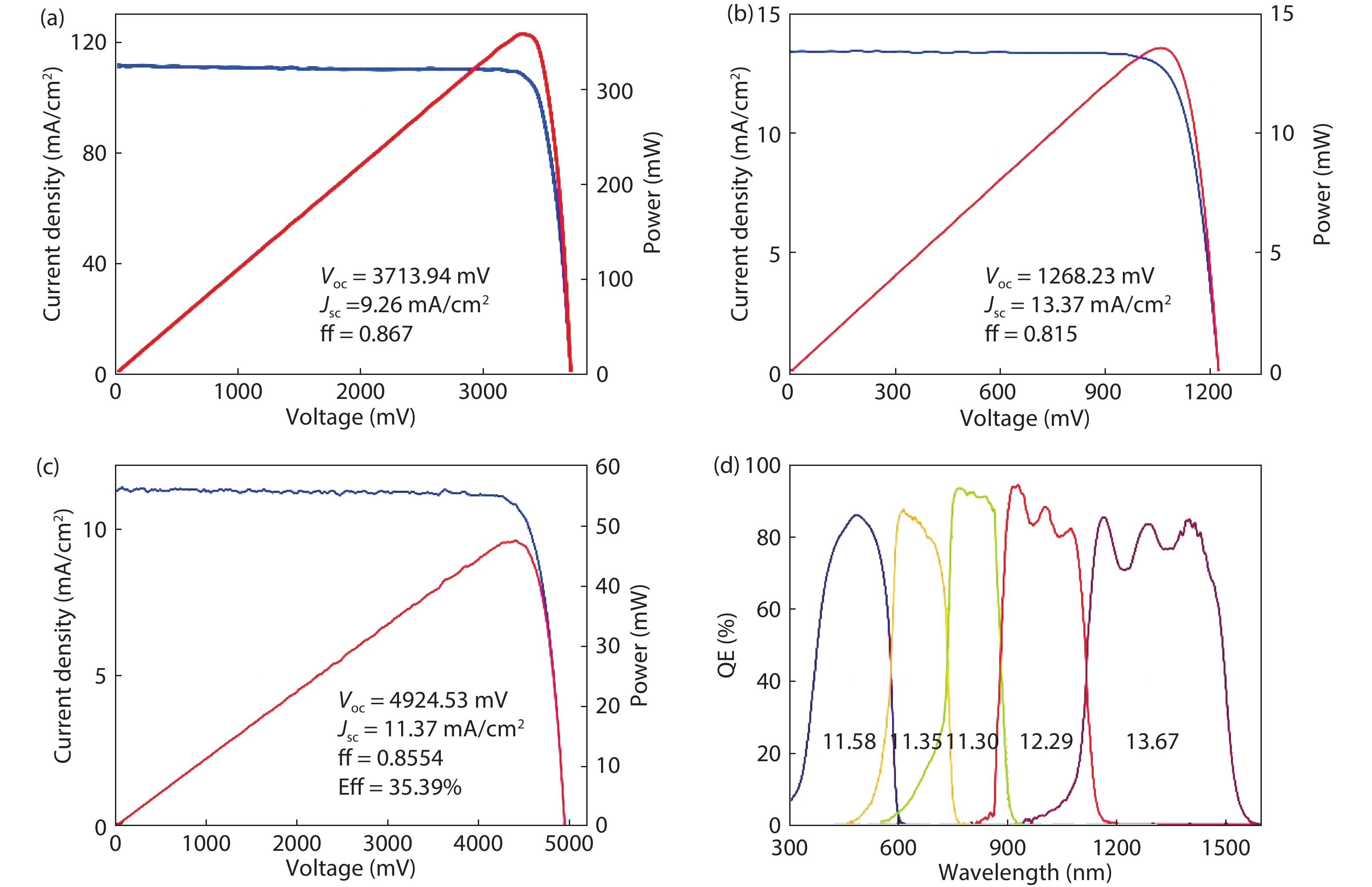
Multijunction solar cells are the highest efficiency photovoltaic devices yet demonstrated for both space and terrestrial applications. In recent years five-junction cells based on the direct semiconductor bonding technique (SBT), demonstrates space efficiencies >35% and presents application potentials. In this paper, the major challenges for fabricating SBT 5J cells and their appropriate strategies involving structure tunning, band engineering and material tailoring are stated, and 4-cm2 35.4% (AM0, one sun) 5J SBT cells are presented. Further efforts on detailed optical managements are required to improve the current generating and matching in subcells, to achieve efficiencies 36%–37%, or above.

J. Semicond.
2021, 42(12): 122801 doi: 10.1088/1674-4926/42/12/122801
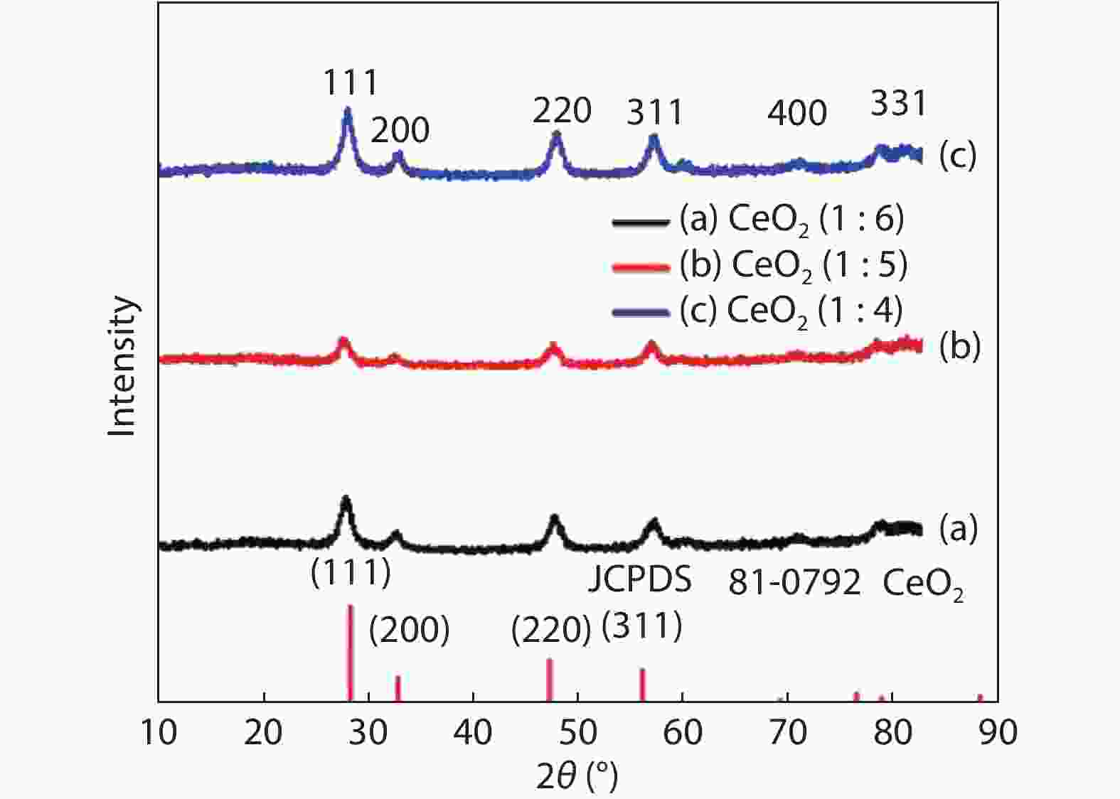
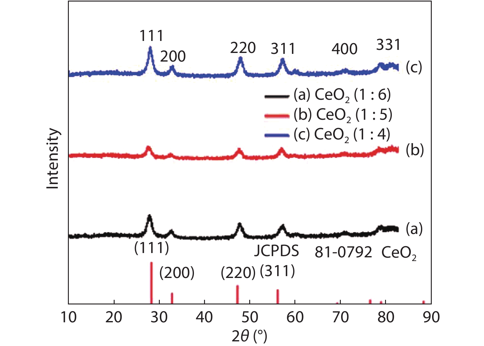
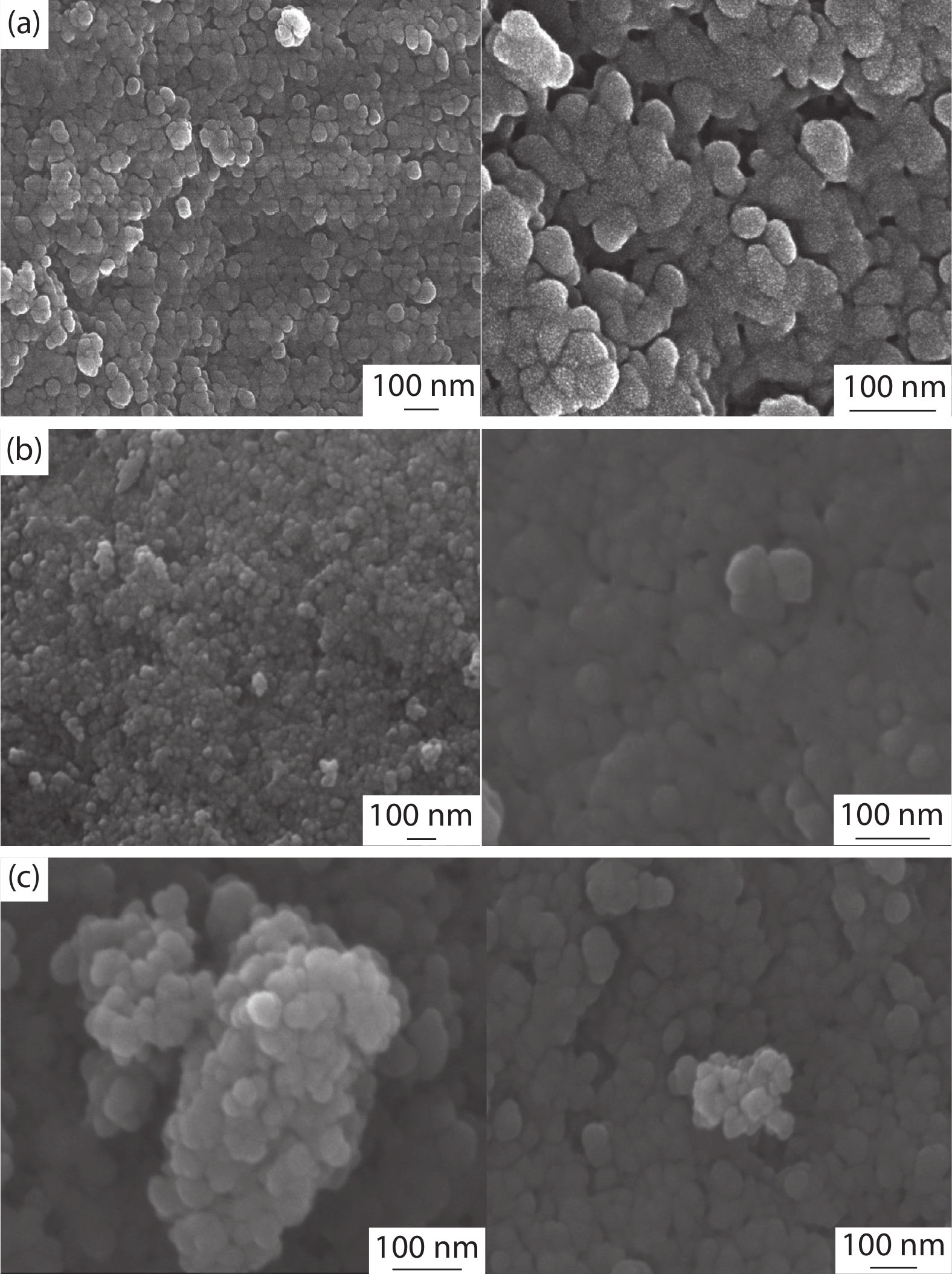
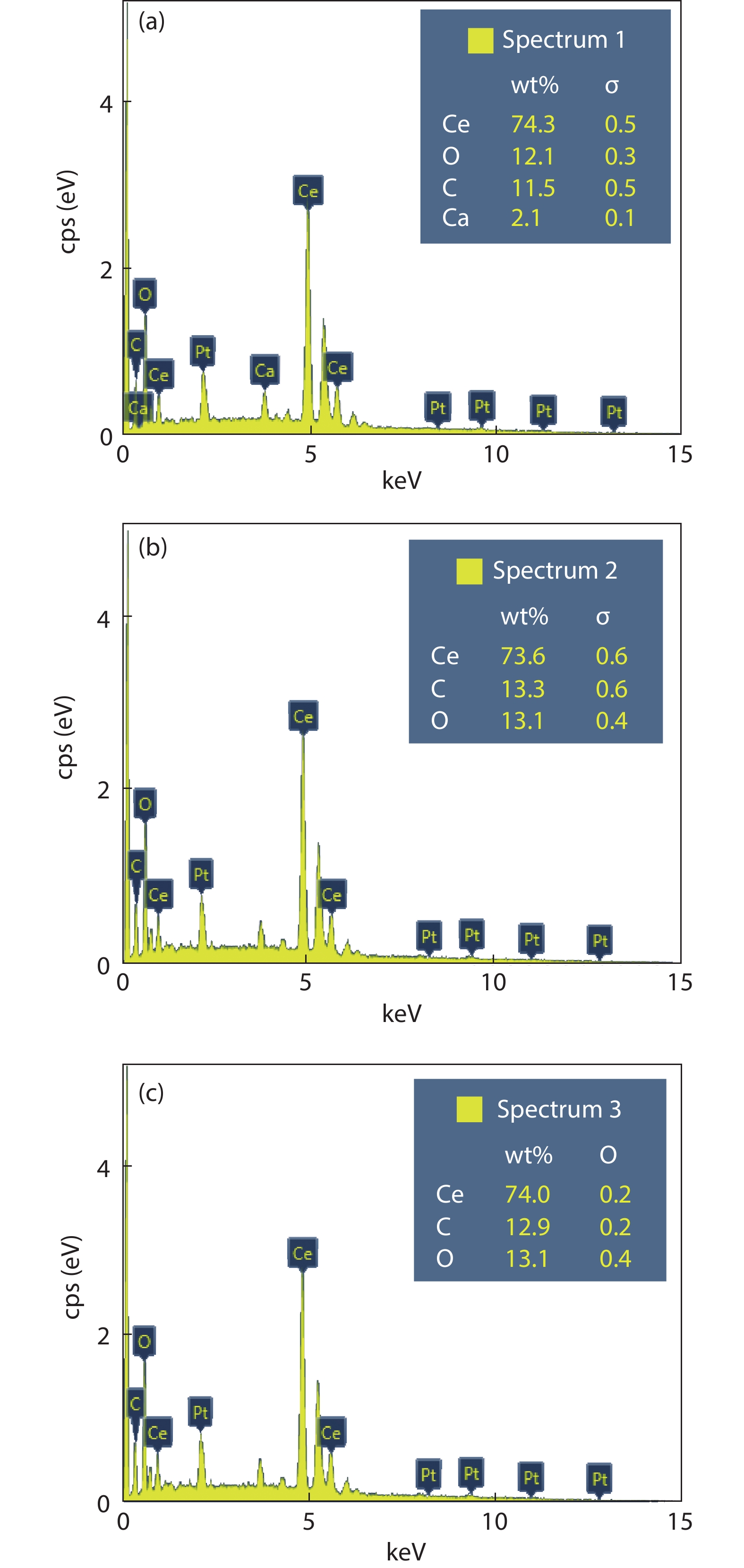
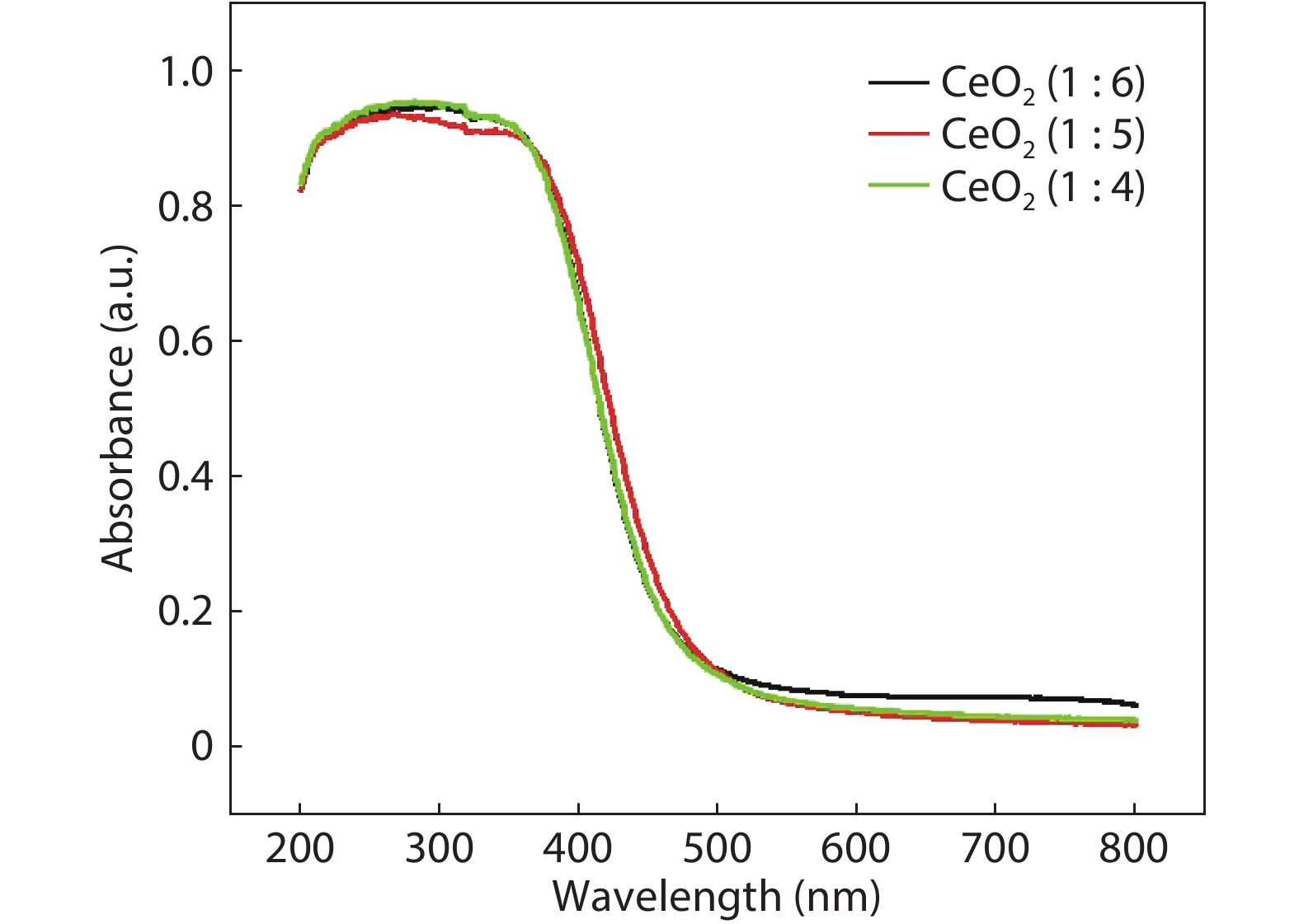
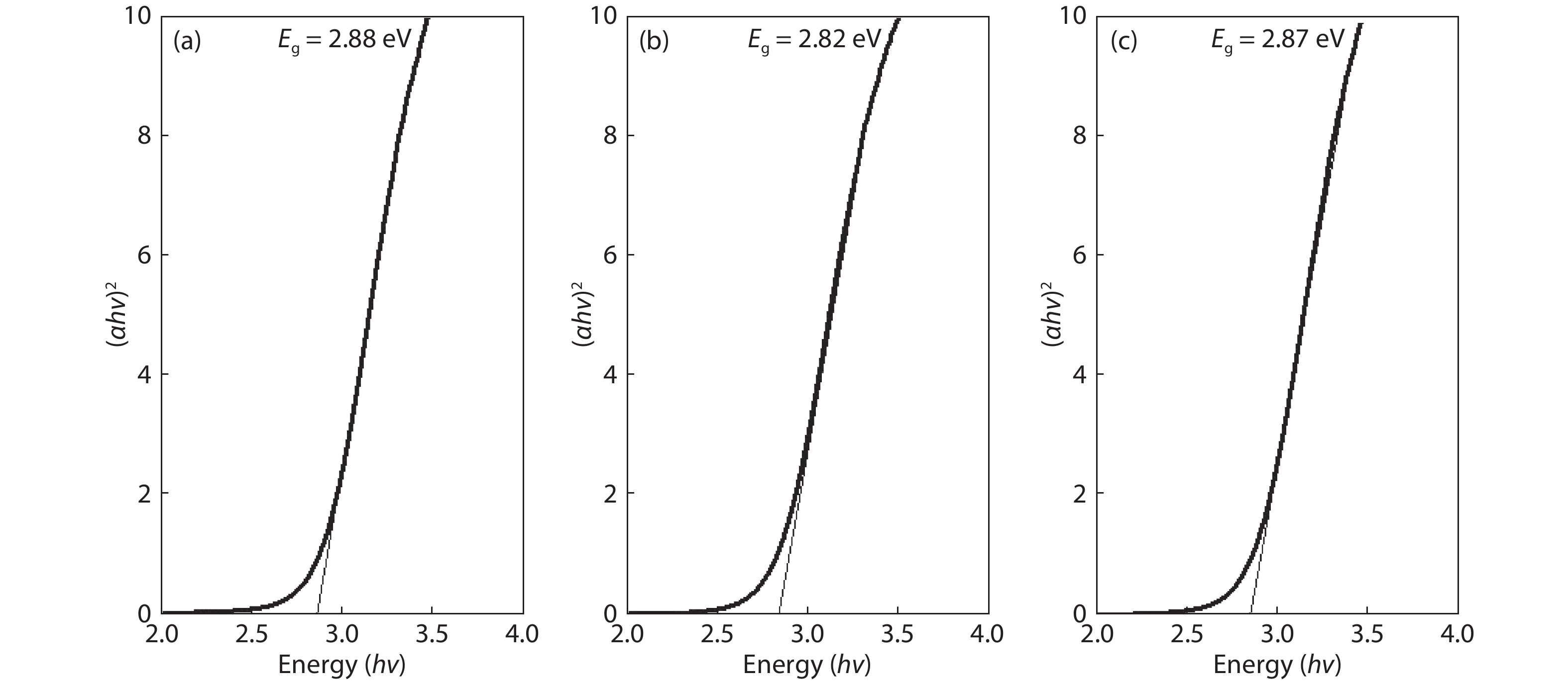
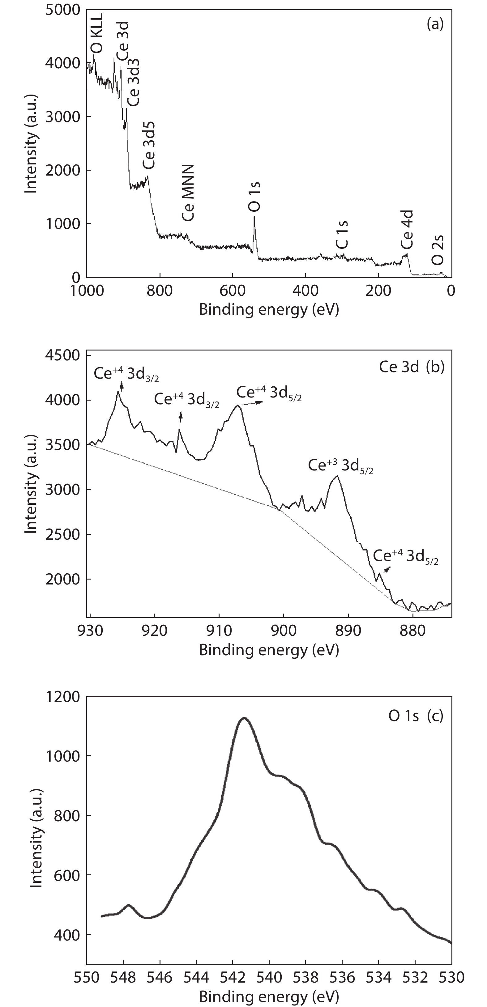
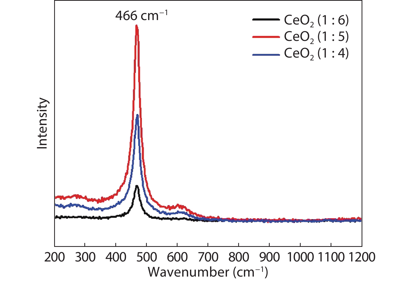
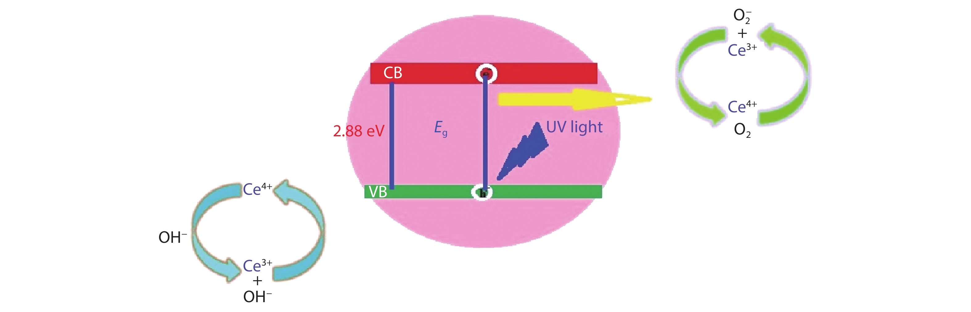
Crystalline cubic cerium oxide nano particles have been synthesized from cerium (III) nitrate (Ce (NO3)3.6H2O) and sodium hydroxide by a hydrothermal method. The effect of three different molar ratios of the NaOH precipitating agent on structural, optical, and photo catalytic activity was investigated. The synthesized cerium oxide nano particles were characterized by X-ray diffraction (XRD), a UV–vis spectrometer, scanning electron microscope (SEM), energy-dispersive X-ray spectroscopy (EDAX), Raman spectroscopy and X-ray photo electron spectroscopy (XPS). According to the findings, hydrothermally synthesized cerium oxide NPs have a high efficiency for photocatalytic degradation of methylene blue when exposed to UV light. Environmental water pollution is the major issue of the atmosphere. To get fresh water, humans could search the resources to purify the water in simple way and degradation is the one of the methods to purify salt water.


J. Semicond.
2021, 42(12): 122802 doi: 10.1088/1674-4926/42/12/122802
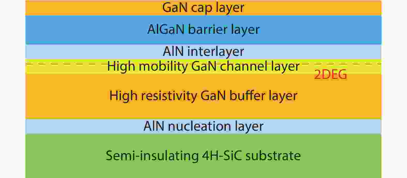
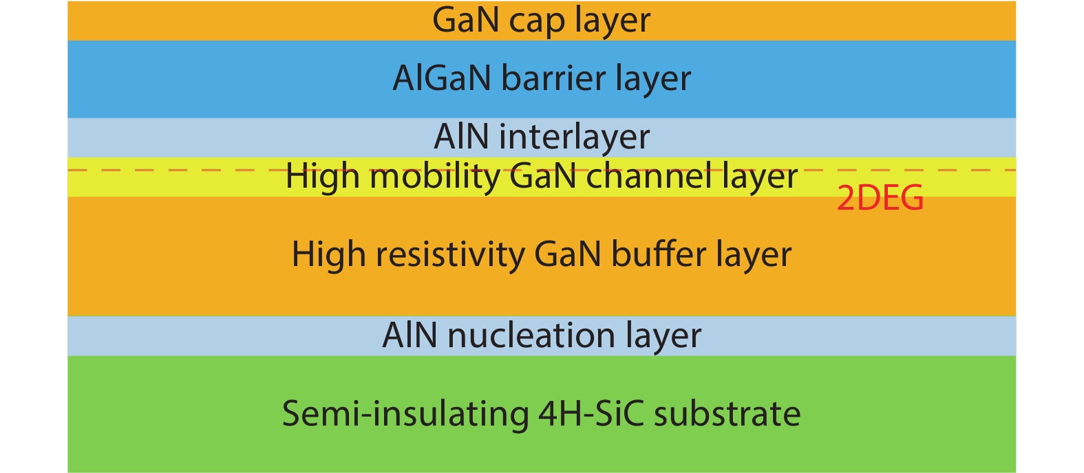
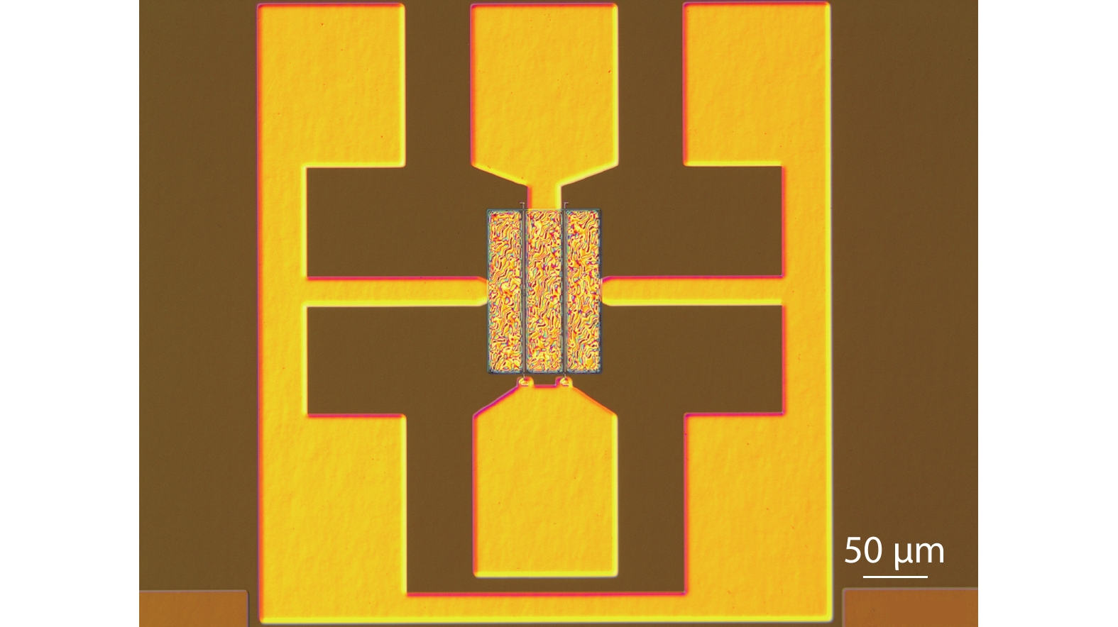
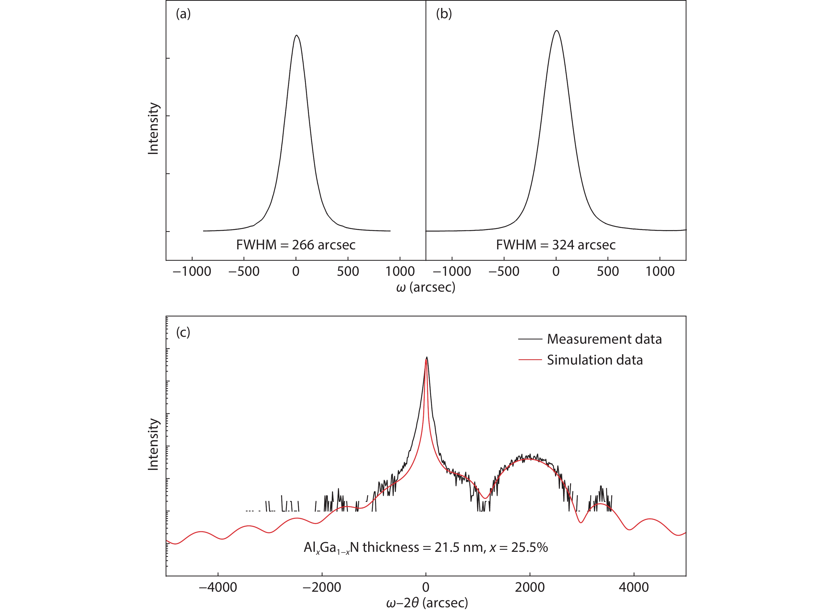
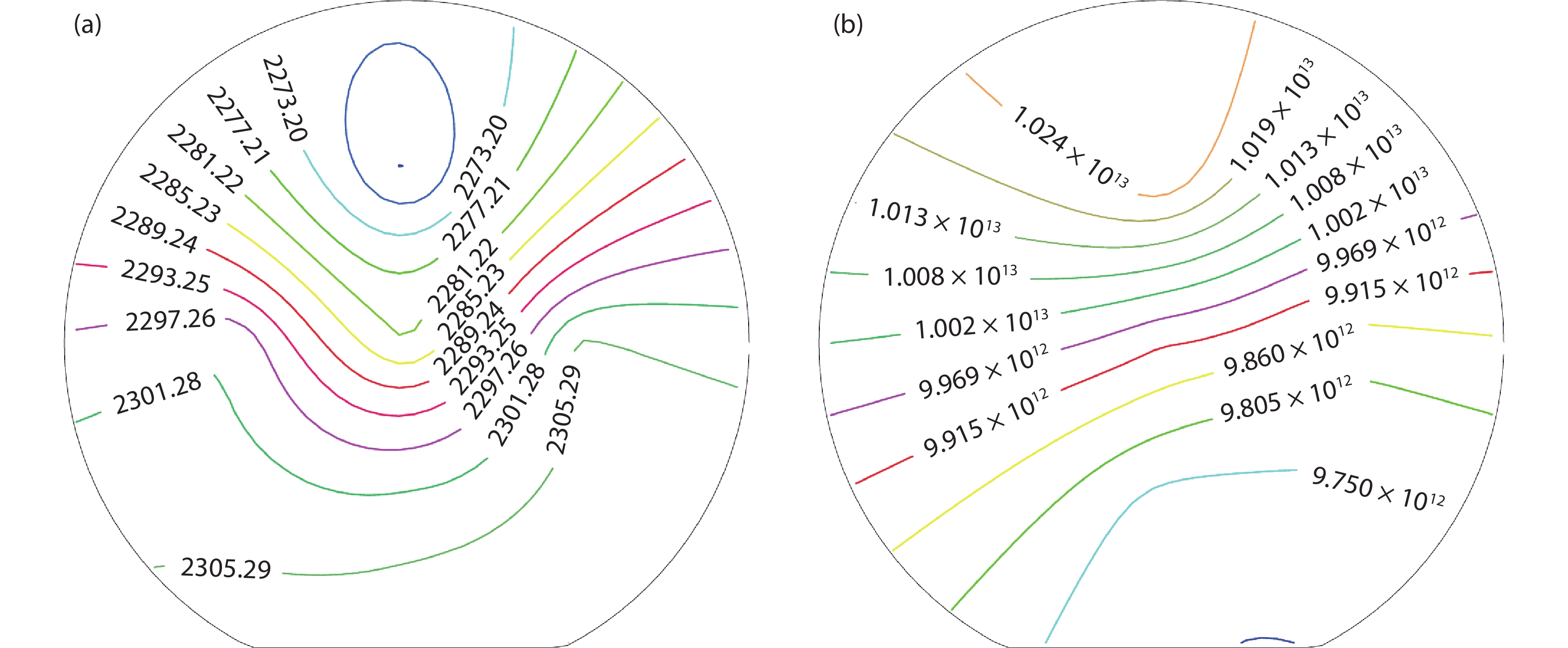
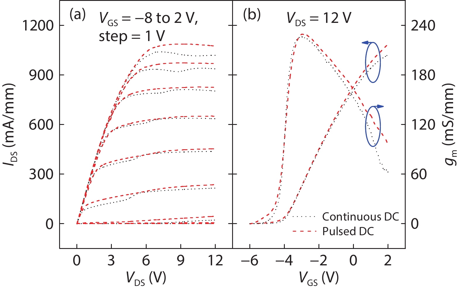
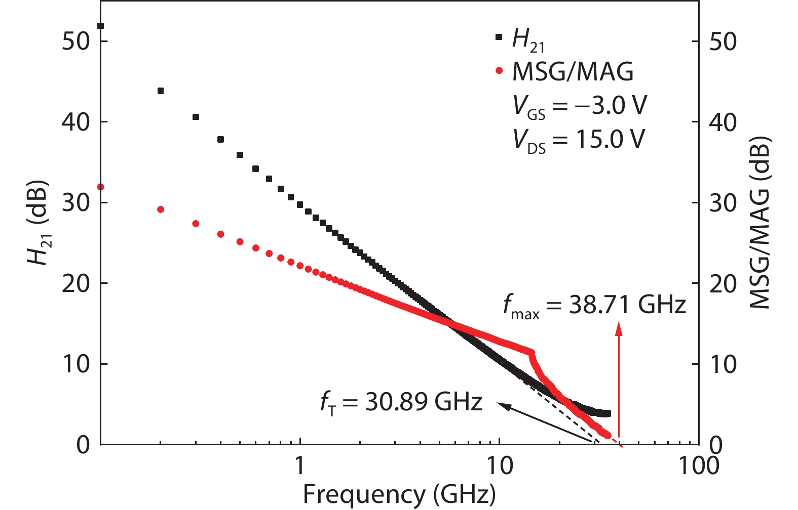
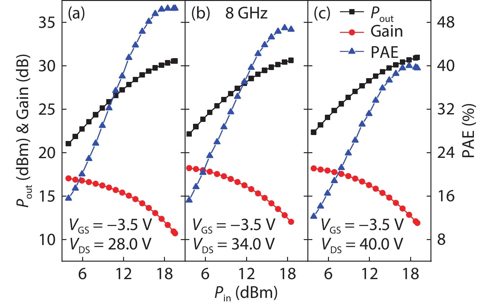
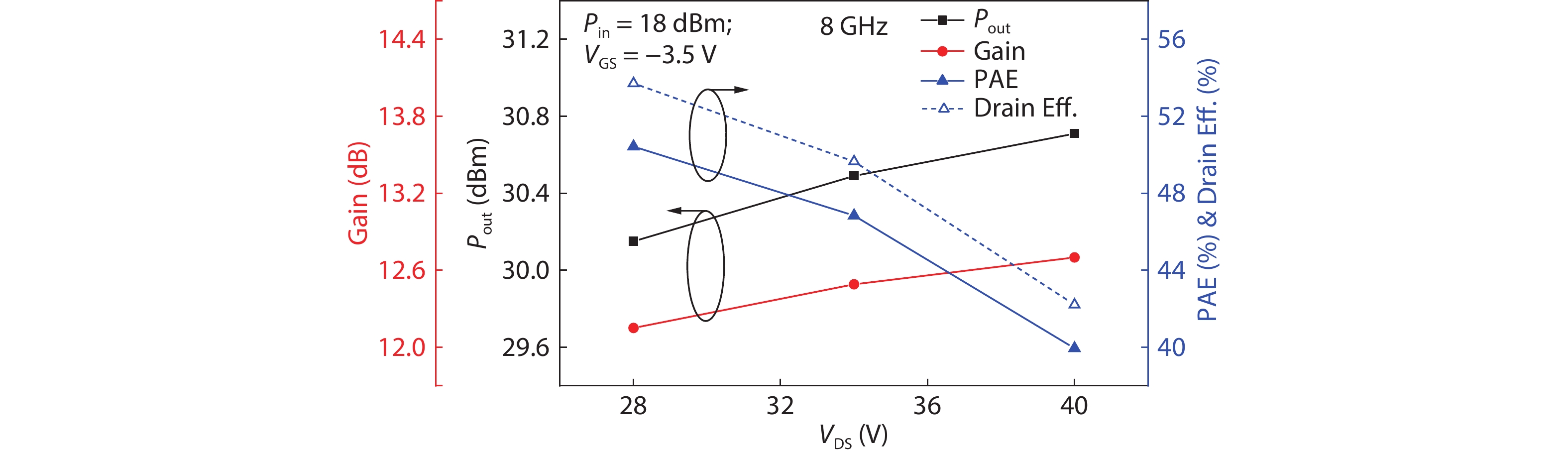
State-of-the-art AlGaN/GaN high electron mobility structures were grown on semi-insulating 4H-SiC substrates by MOCVD and X-band microwave power high electron mobility transistors were fabricated and characterized. Hall mobility of 2291.1 cm2/(V·s) and two-dimensional electron gas density of 9.954 × 1012 cm–2 were achieved at 300 K. The HEMT devices with a 0.45-μm gate length exhibited maximum drain current density as high as 1039.6 mA/mm and peak extrinsic transconductance of 229.7 mS/mm. The fT of 30.89 GHz and fmax of 38.71 GHz were measured on the device. Load-pull measurements were performed and analyzed under (–3.5, 28) V, (–3.5, 34) V and (–3.5, 40) V gate/drain direct current bias in class-AB, respectively. The uncooled device showed high linear power gain of 17.04 dB and high power-added efficiency of 50.56% at 8 GHz when drain biased at (–3.5, 28) V. In addition, when drain biased at (–3.5, 40) V, the device exhibited a saturation output power density up to 6.21 W/mm at 8 GHz, with a power gain of 11.94 dB and a power-added efficiency of 39.56%. Furthermore, the low fmax/fT ratio and the variation of the power sweep of the device at 8 GHz with drain bias voltage were analyzed.

J. Semicond.
2021, 42(12): 122803 doi: 10.1088/1674-4926/42/12/122803
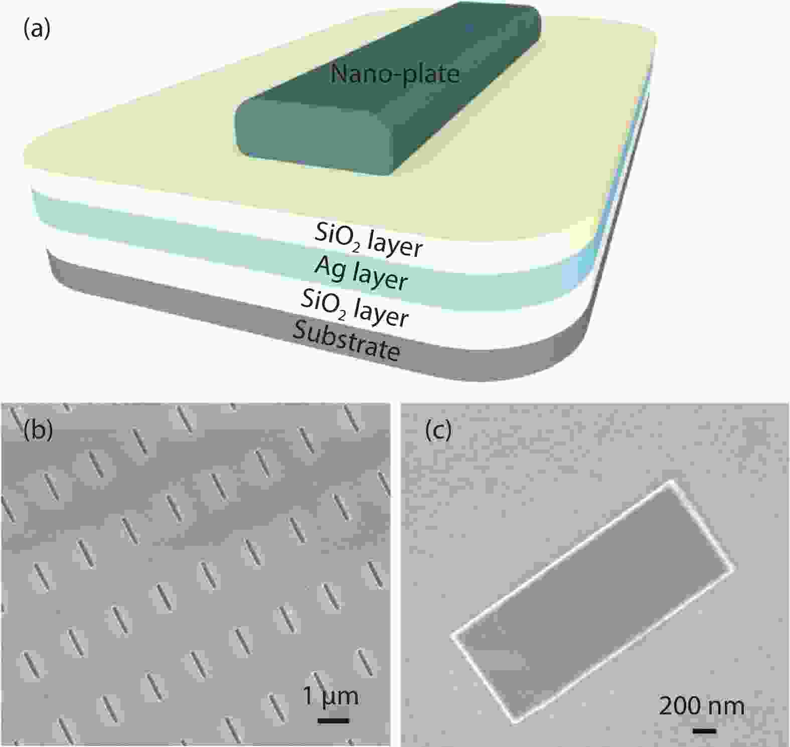
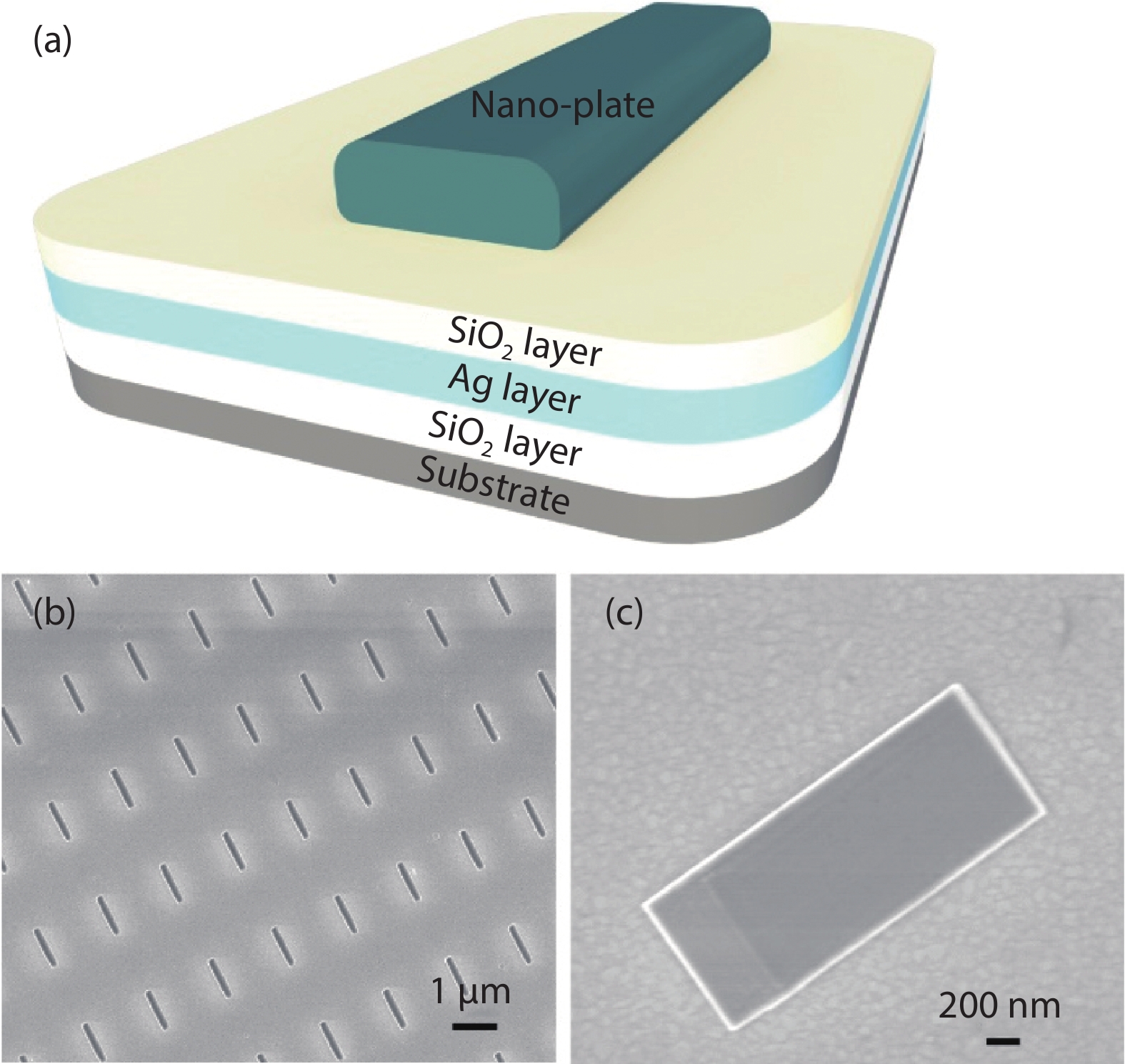
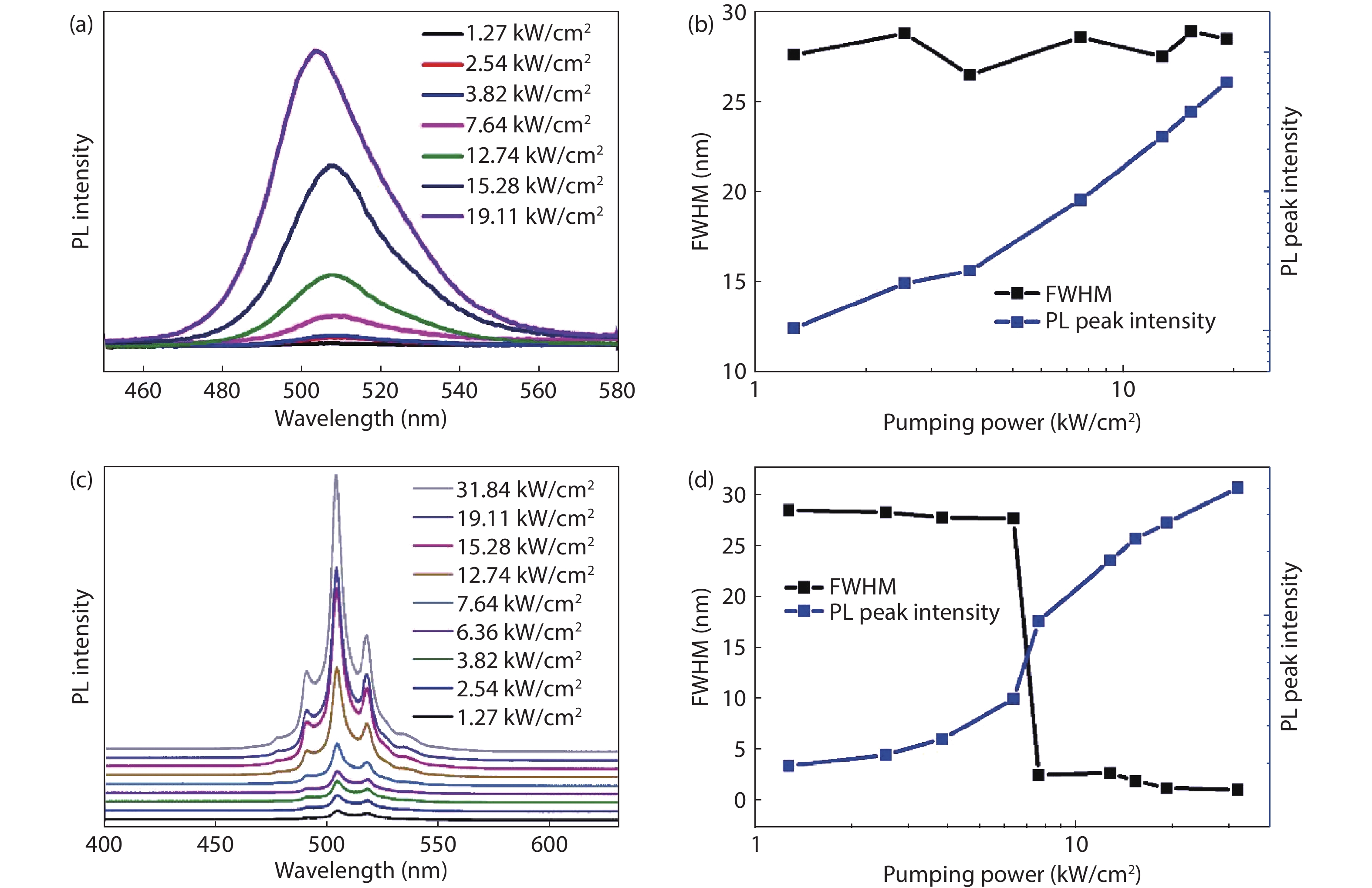
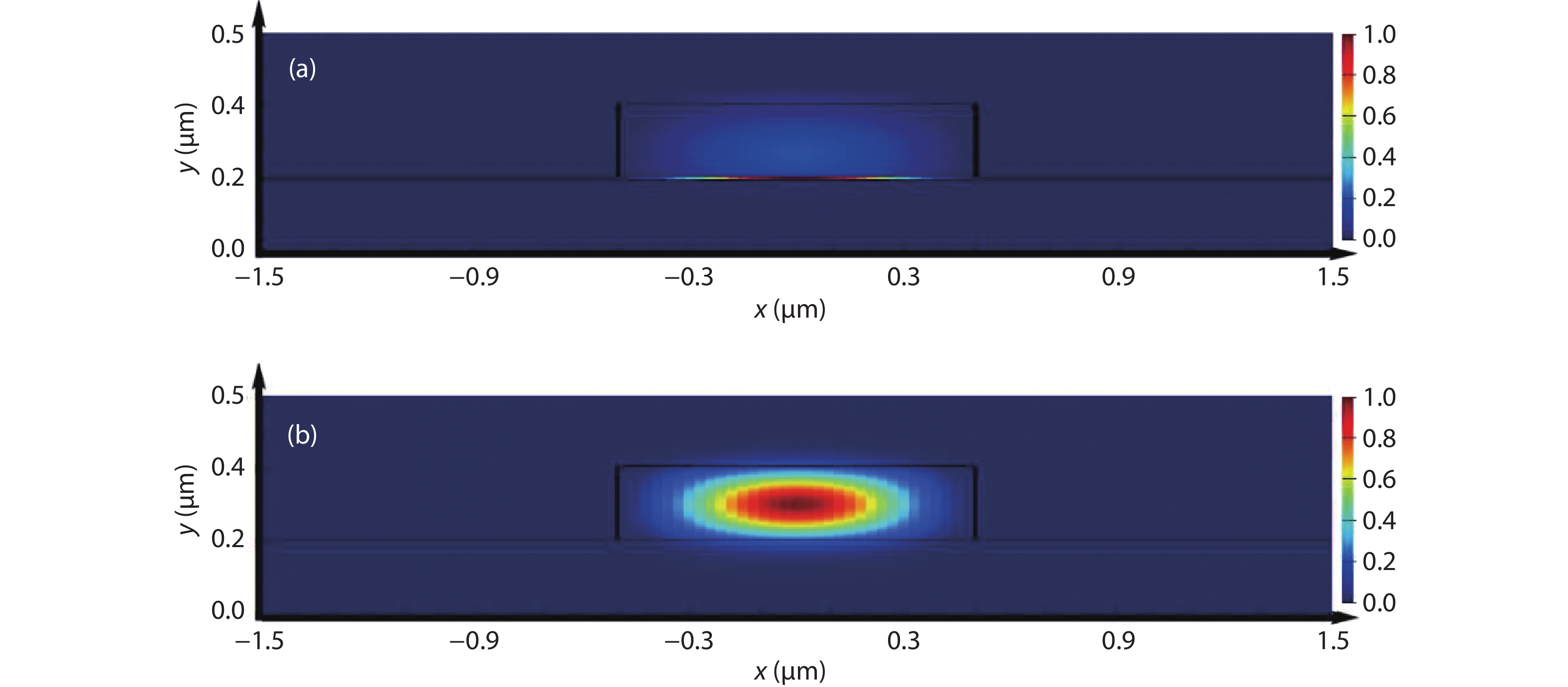
Plasmonic nanolaser as a new type of ultra-small laser, has gain wide interests due to its breaking diffraction limit of light and fast carrier dynamics characters. Normally, the main problem that need to be solved for plasmonic nanolaser is high loss induced by optical and ohmic losses, which leads to the low quality factor. In this work, InGaN/GaN nanoplate plasmonic nanolaser with large interface area were designed and fabricated, where the overlap between SPs and excitons can be enhanced. The lasing threshold is calculated to be ~6.36 kW/cm2, where the full width at half maximum (FWHM) drops from 27 to 4 nm. And the fast decay time at 502 nm (sharp peak of stimulated lasing) is estimated to be 0.42 ns. Enhanced lasing characters are mainly attributed to the strong confinement of electromagnetic wave in the low refractive index material, which improve the near field coupling between SPs and excitons. Such plasmonic laser should be useful in data storage applications, biological application, light communication, especially for optoelectronic devices integrated into a system on a chip.

J. Semicond.
2021, 42(12): 122804 doi: 10.1088/1674-4926/42/12/122804
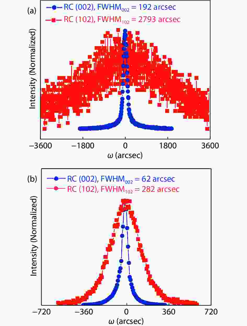
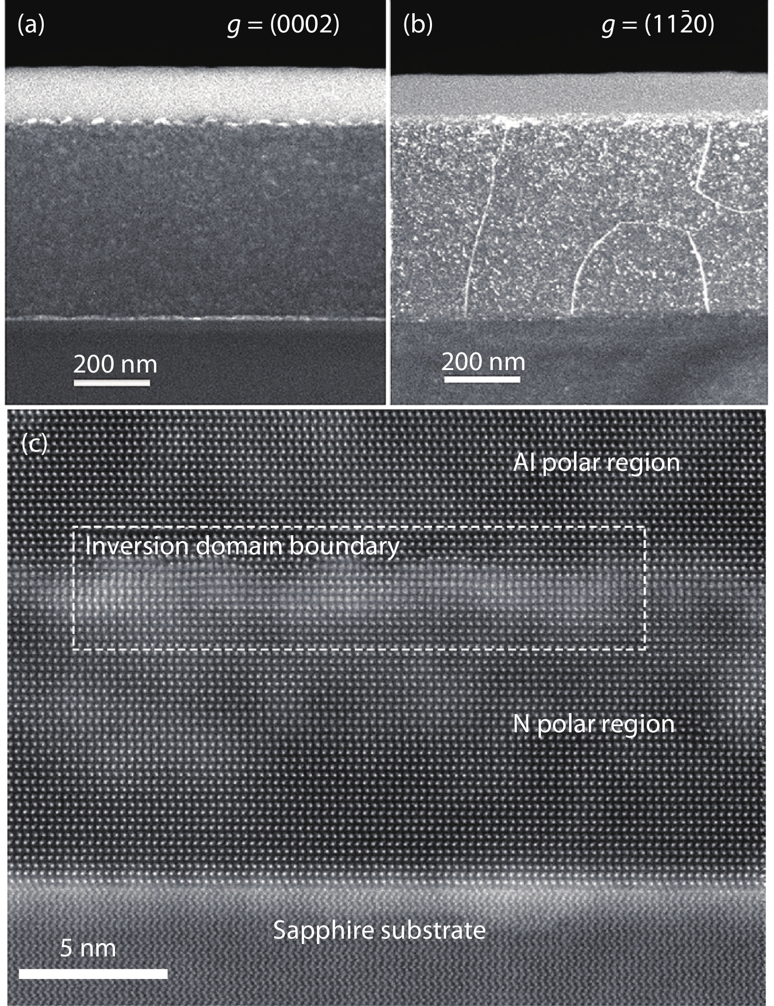
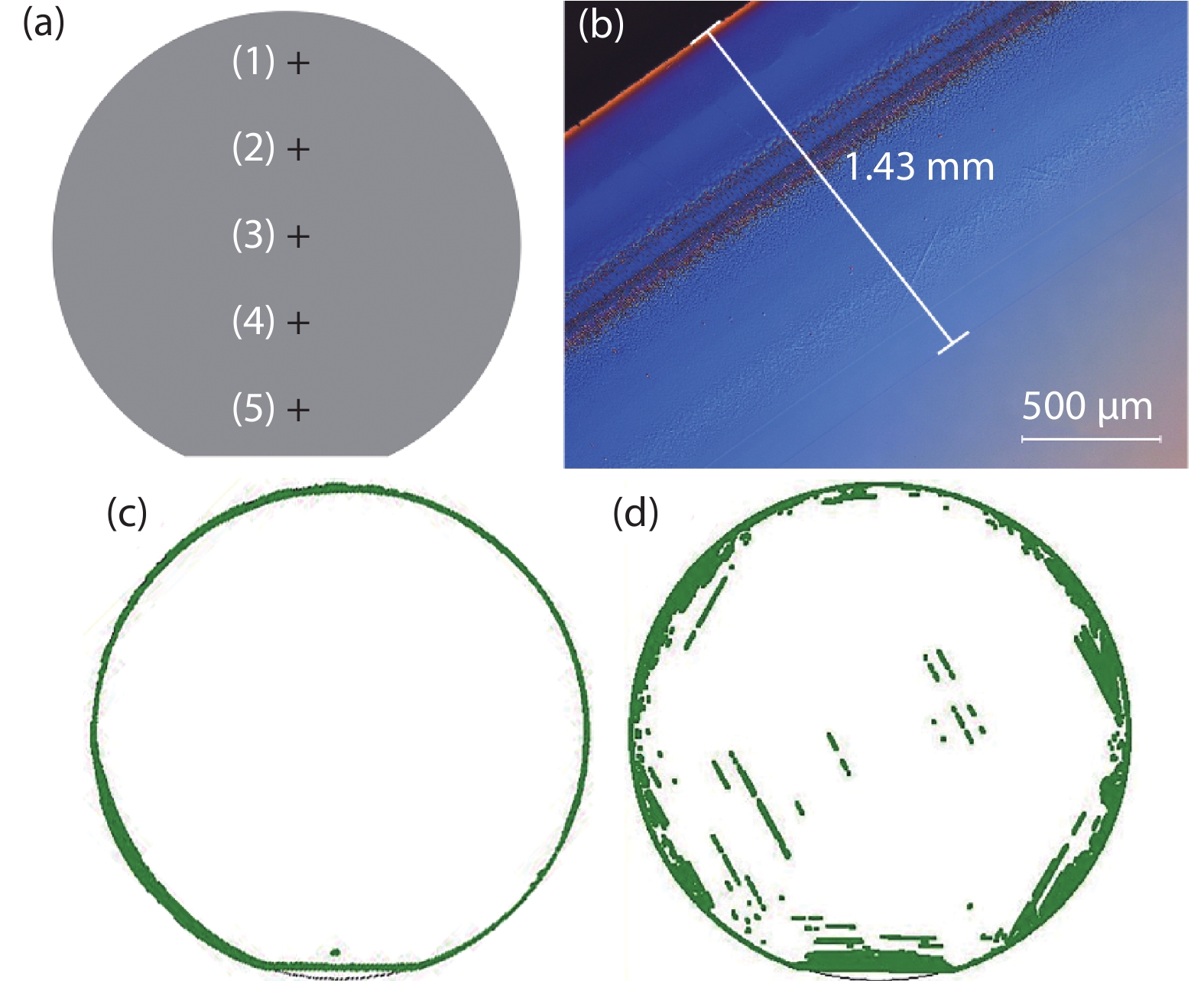
In this work, based on physical vapor deposition and high-temperature annealing (HTA), the 4-inch crack-free high-quality AlN template is initialized. Benefiting from the crystal recrystallization during the HTA process, the FWHMs of X-ray rocking curves for (002) and (102) planes are encouragingly decreased to 62 and 282 arcsec, respectively. On such an AlN template, an ultra-thin AlN with a thickness of ~700 nm grown by MOCVD shows good quality, thus avoiding the epitaxial lateral overgrowth (ELOG) process in which 3–4 μm AlN is essential to obtain the flat surface and high crystalline quality. The 4-inch scaled wafer provides an avenue to match UVC-LED with the fabrication process of traditional GaN-based blue LED, therefore significantly improving yields and decreasing cost.


J. Semicond.
2021, 42(12): 122805 doi: 10.1088/1674-4926/42/12/122805
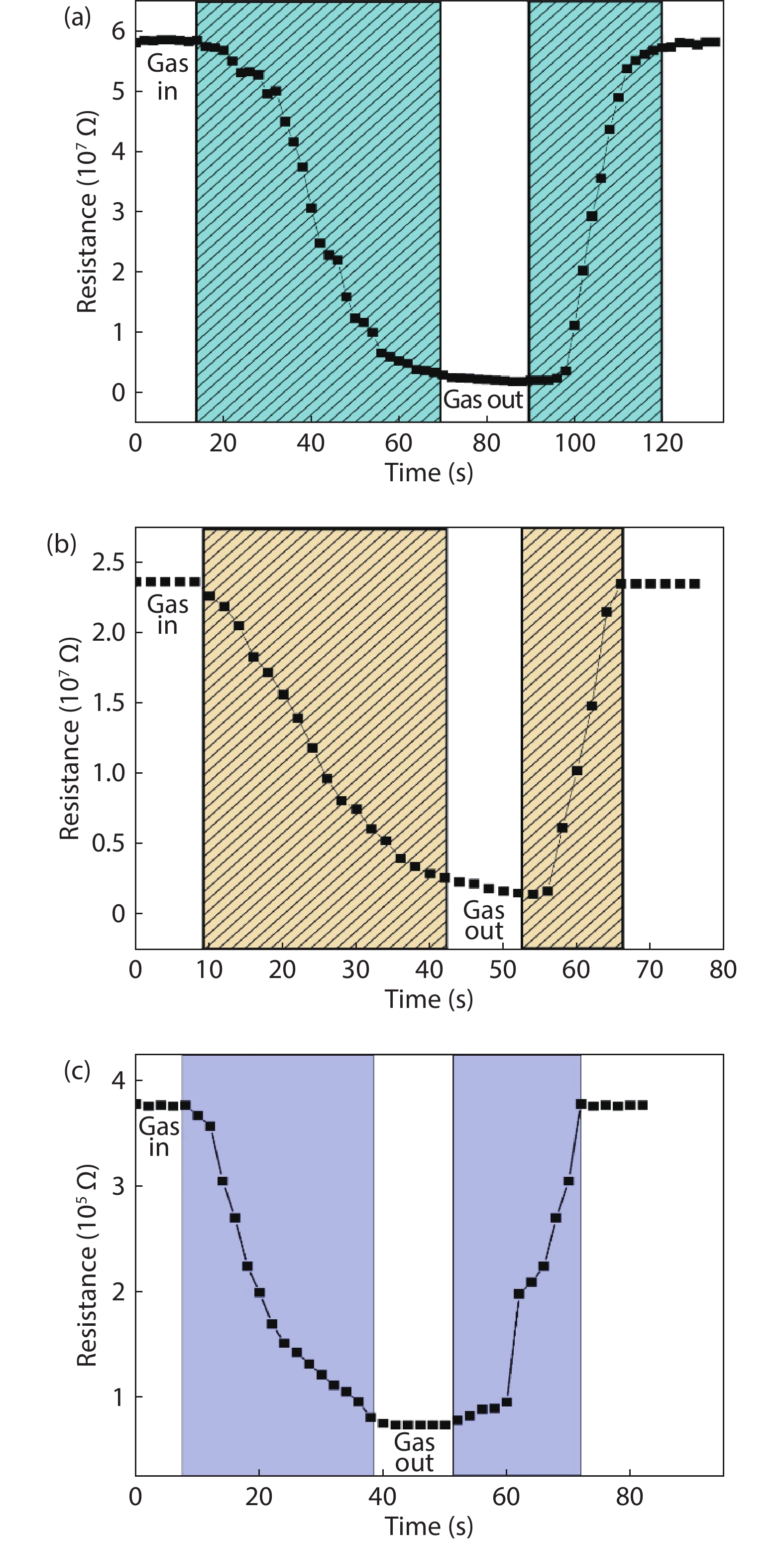
In the present work, ferrite (Fe) doped TiO2 thin films with different volume percentage (vol%) were synthesized using a spray pyrolysis technique. The effect of Fe doping on structural properties such as crystallite size, texture coefficient, microstrain, dislocation densities etc. were evaluated from the X ray diffratometry (XRD) data. XRD data revealed a polycrystalline anatase TiO2 phase for sample synthesized up to 2 vol% and mixed anatase and rutile crystalline phase for sample synthesized at 4 vol% Fe doped TiO2. The crystalline size was observed to decrease with increase in Fe dopant vol% and also other structural parameters changes with Fe dopant percentage. In the present work, electrical resistance was observed to decrease with a rise in Fe dopant vol% and temperature of the sample. Thermal properties like temperature coefficient of resistance and activation energy also showed strong correlation with Fe dopant vol%. Humidity sensing properties of the synthesized sample altered with a change in Fe dopant vol%. In the present paper, maximum sensitivity of about 88.7% for the sample synthesized with 2 vol% Fe doped TiO2 and also the lowest response and recovery time of about 52 and 3 s were reported for the same sample.
J. Semicond.
2021, 42(12): 122901 doi: 10.1088/1674-4926/42/12/122901
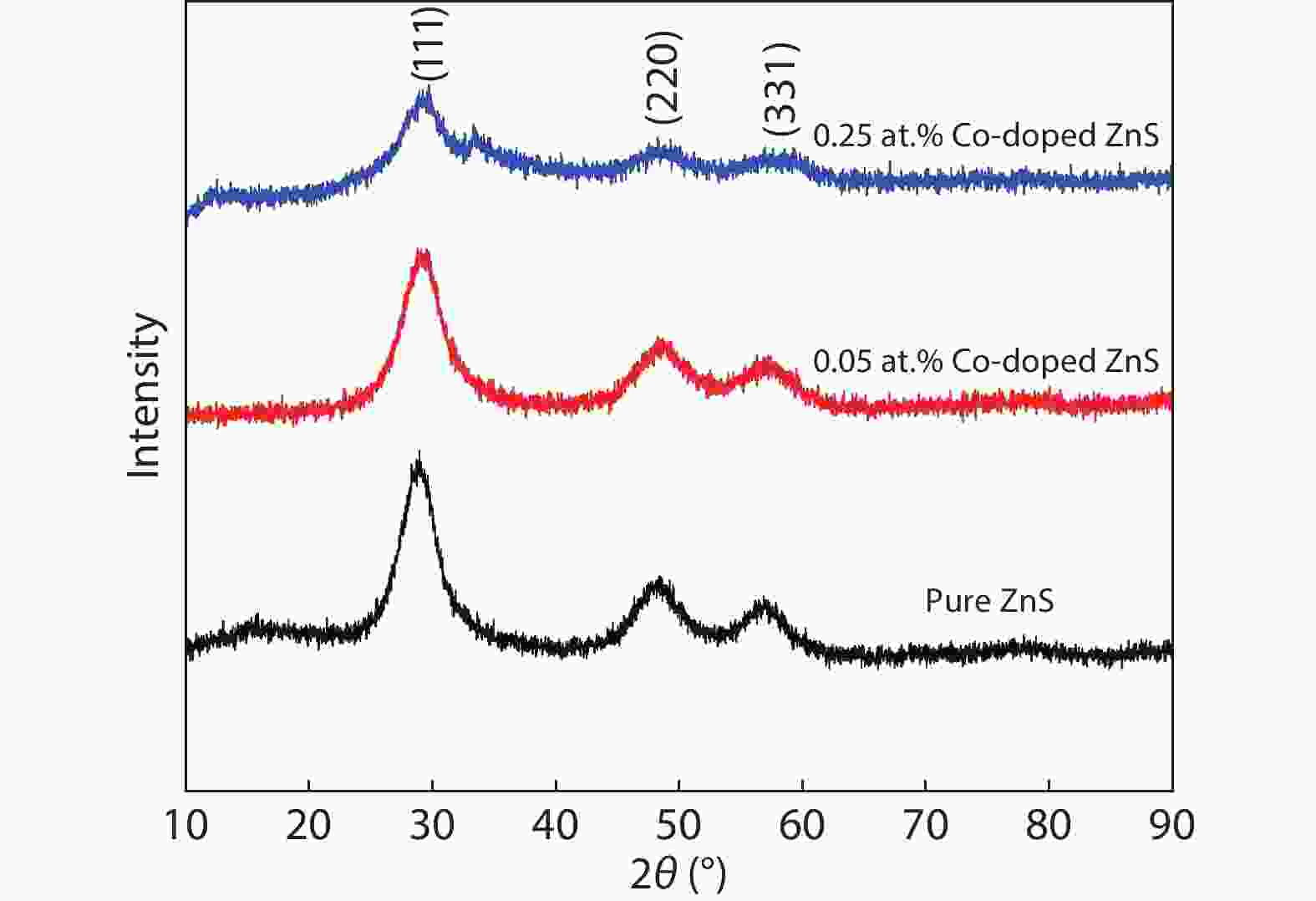
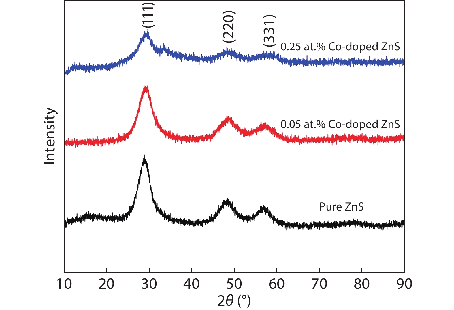
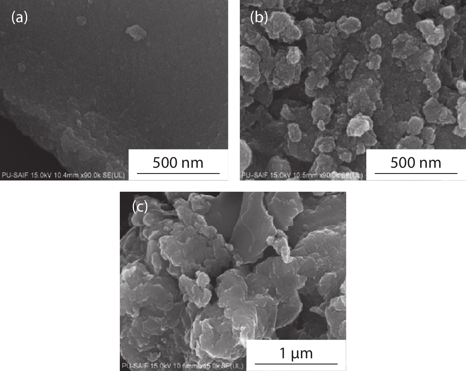
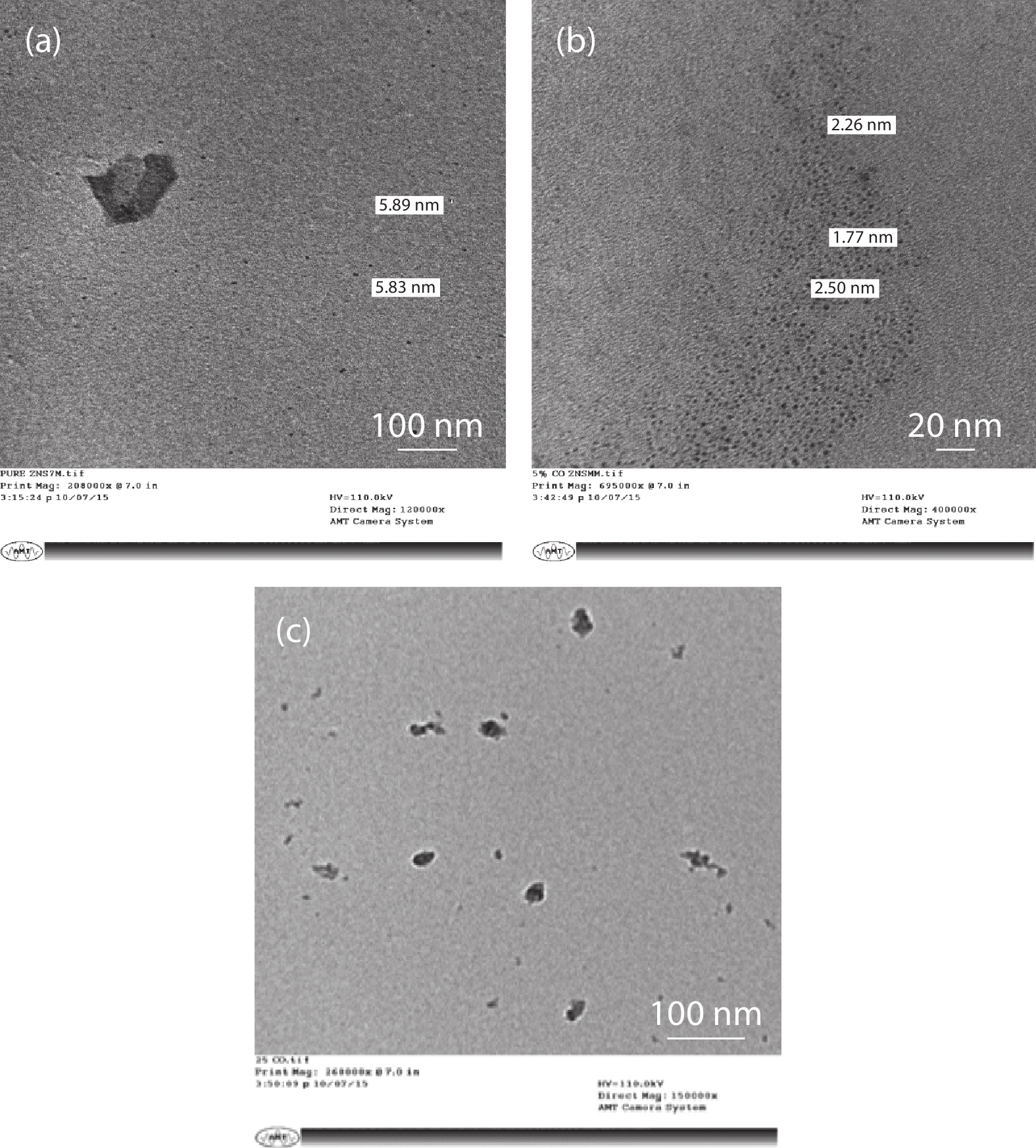
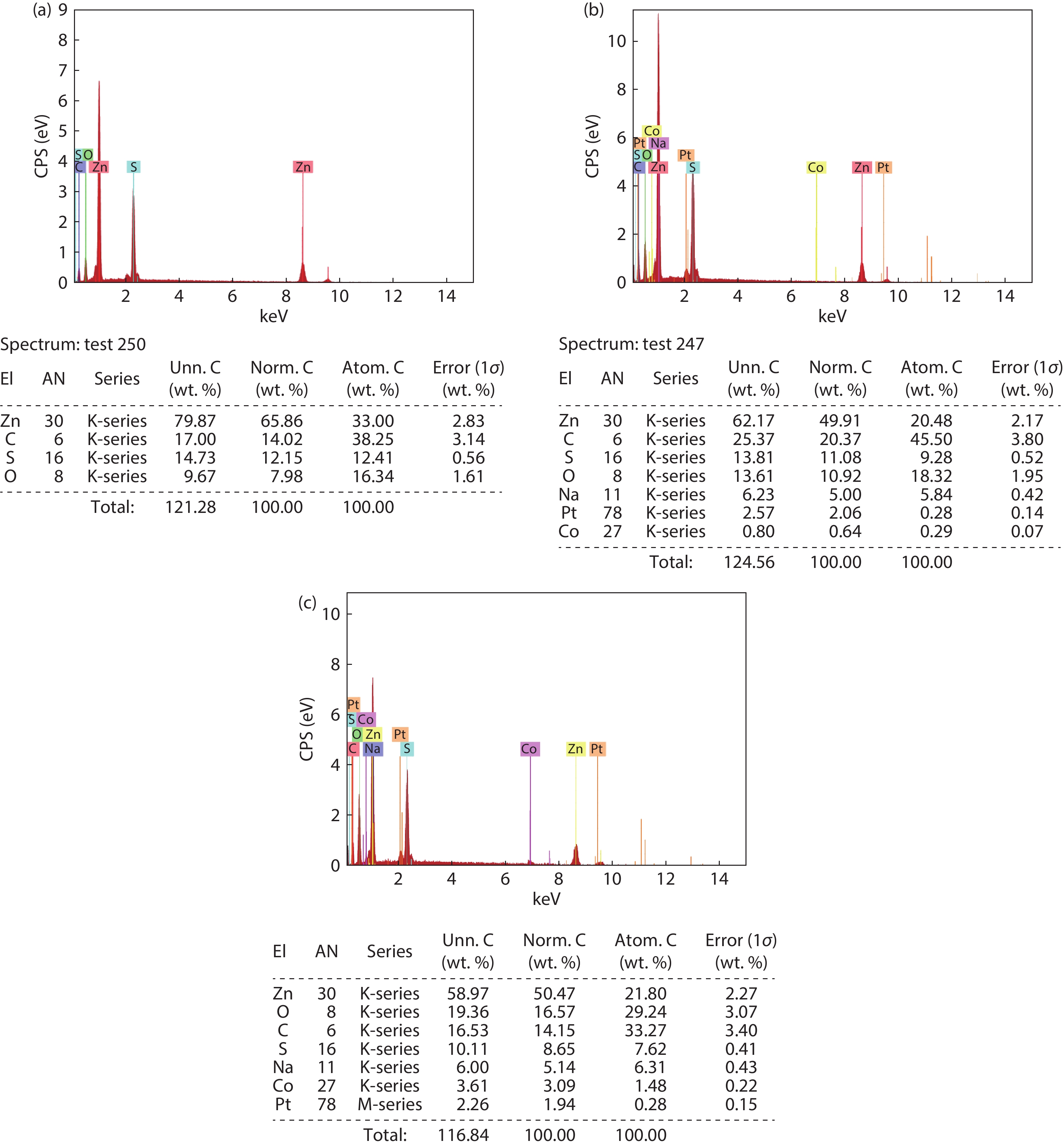
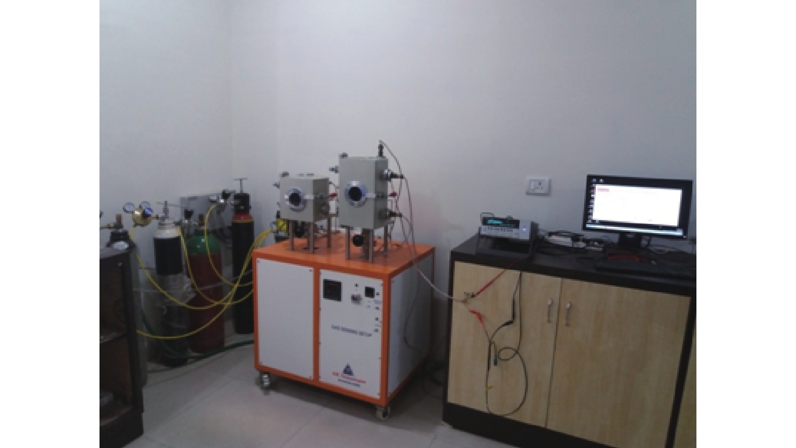
In the present work, a solution-based co-precipitation method has been adopted to synthesize pure and cobalt-doped ZnS quantum dots and characterized by XRD, SEM, TEM with EDX, FTIR and gas sensing properties. XRD analysis has shown a single phase of ZnS quantum dots having a zinc blend structure. TEM and XRD line broadening indicated that the average crystallite size in the sample is in the range of 2 to 5 nm. SEM micrographs show spherical-shaped quantum dots. FTIR studies show that cobalt has been successfully doped into the ZnS cubic lattice. EDX spectra have analyzed the elemental presence in the samples and it is evident that the spectra confirmed the presence of cobalt (Co), zinc (Zn), oxygen (O), and sulphur (S) elements only and no other impurities are observed. The ZnS-based quantum dot sensors reveal high sensitivity towards 50 ppm of ammonia vapors at an operating temperature of 70 °C. Hence, ZnS-based quantum dots can be a promising and quick traceable sensor towards ammonia sensing applications with good response and recovery time.


J. Semicond.
2021, 42(12): 122902 doi: 10.1088/1674-4926/42/12/122902
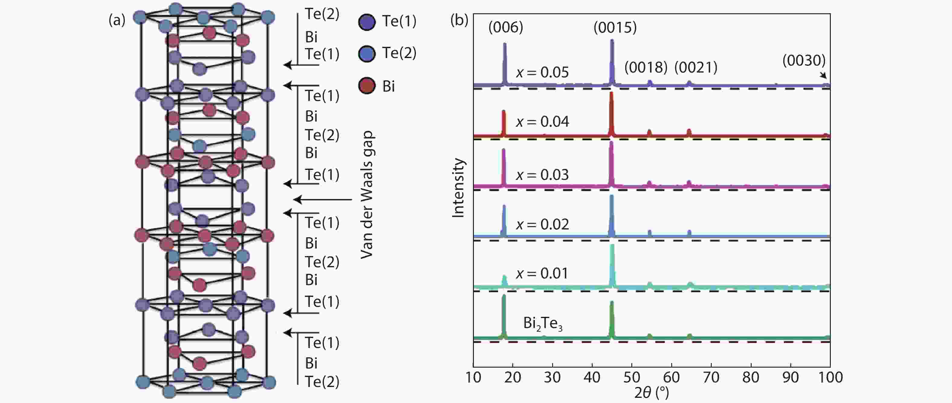
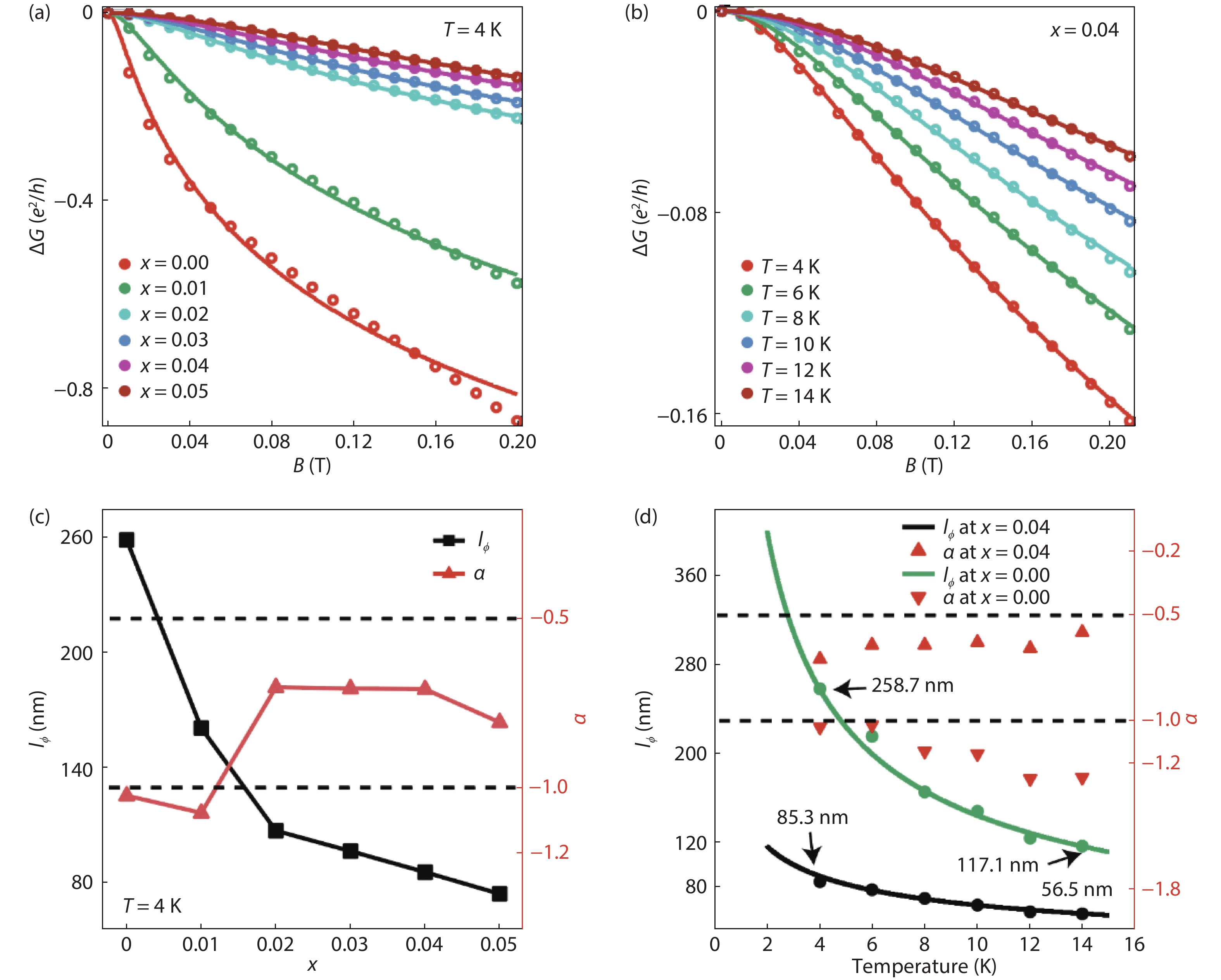
Introducing magnetism into topological insulators (TIs) can tune the topological surface states and produce exotic physical effects. Rare earth elements are considered as important dopant candidates, due to their large magnetic moments from heavily shielded 4f electrons. As the first element with just one 4f electron, cerium (Ce) offers an ideal platform for exploring the doping effect of f-electron in TIs. Here in this work, we have grown cerium-doped topological insulator Bi2Te3 thin films on an Al2O3(0001) substrate by molecular beam epitaxy (MBE). Electronic transport measurements revealed the Kondo effect, weak anti-localization (WAL) effect and suppression of surface conducting channels by Ce doping. Our research shows the fundamental doping effects of Ce in Bi2Te3 thin films, and demonstrates that such a system could be a good platform for further research.

J. Semicond.
2021, 42(12): 124101 doi: 10.1088/1674-4926/42/12/124101
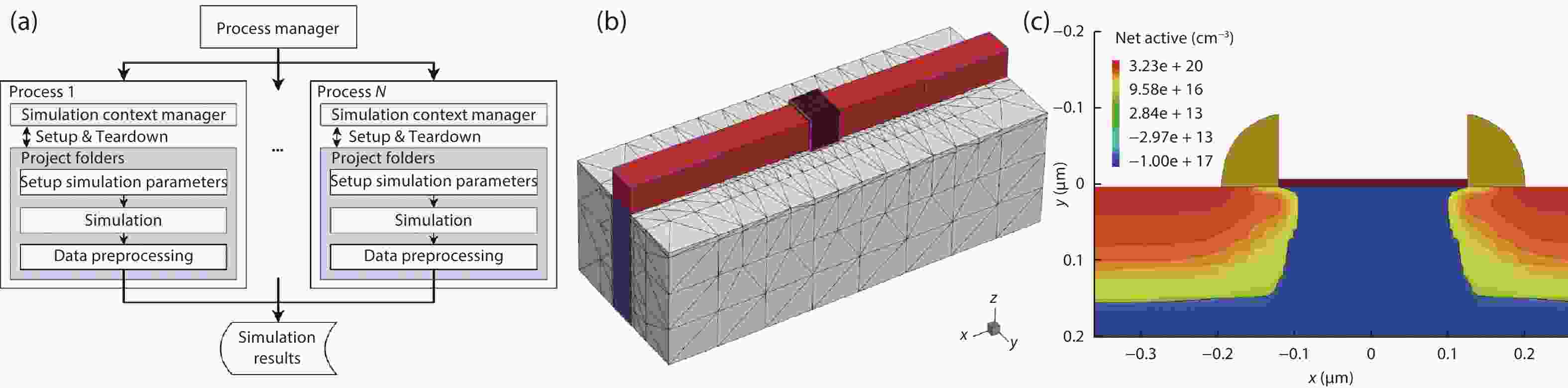
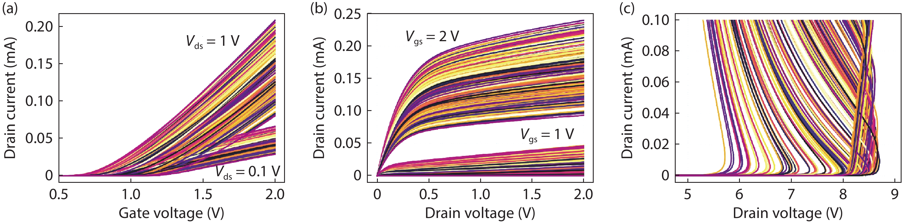
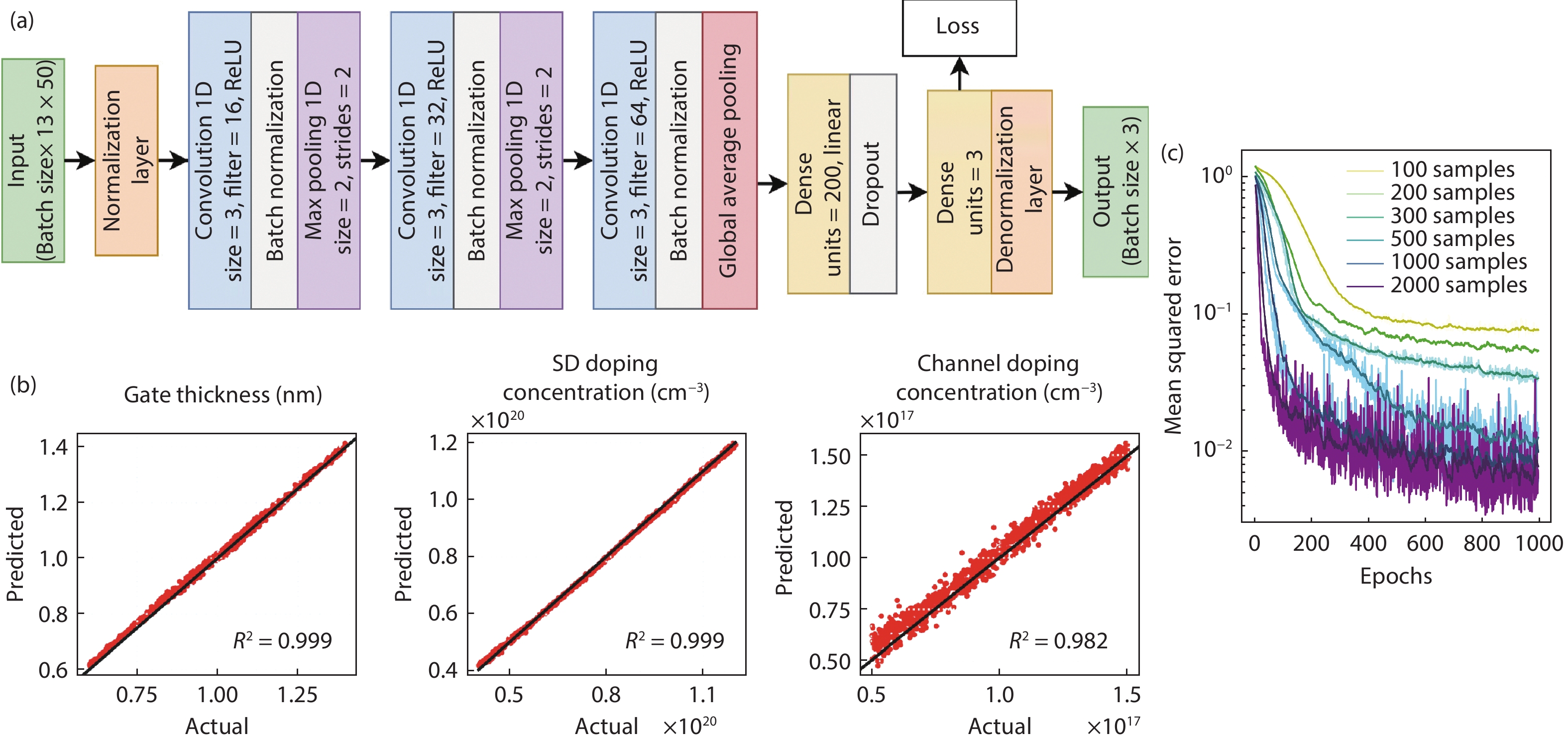
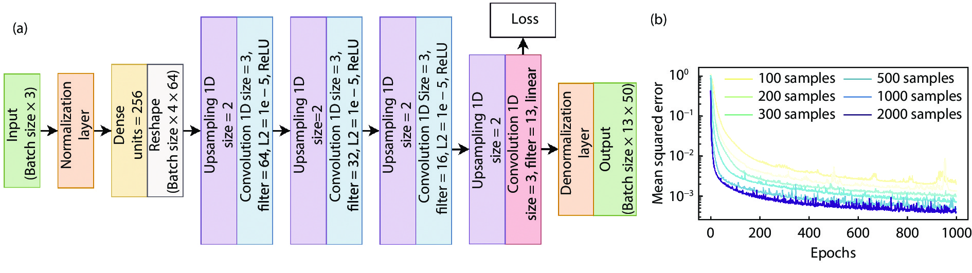
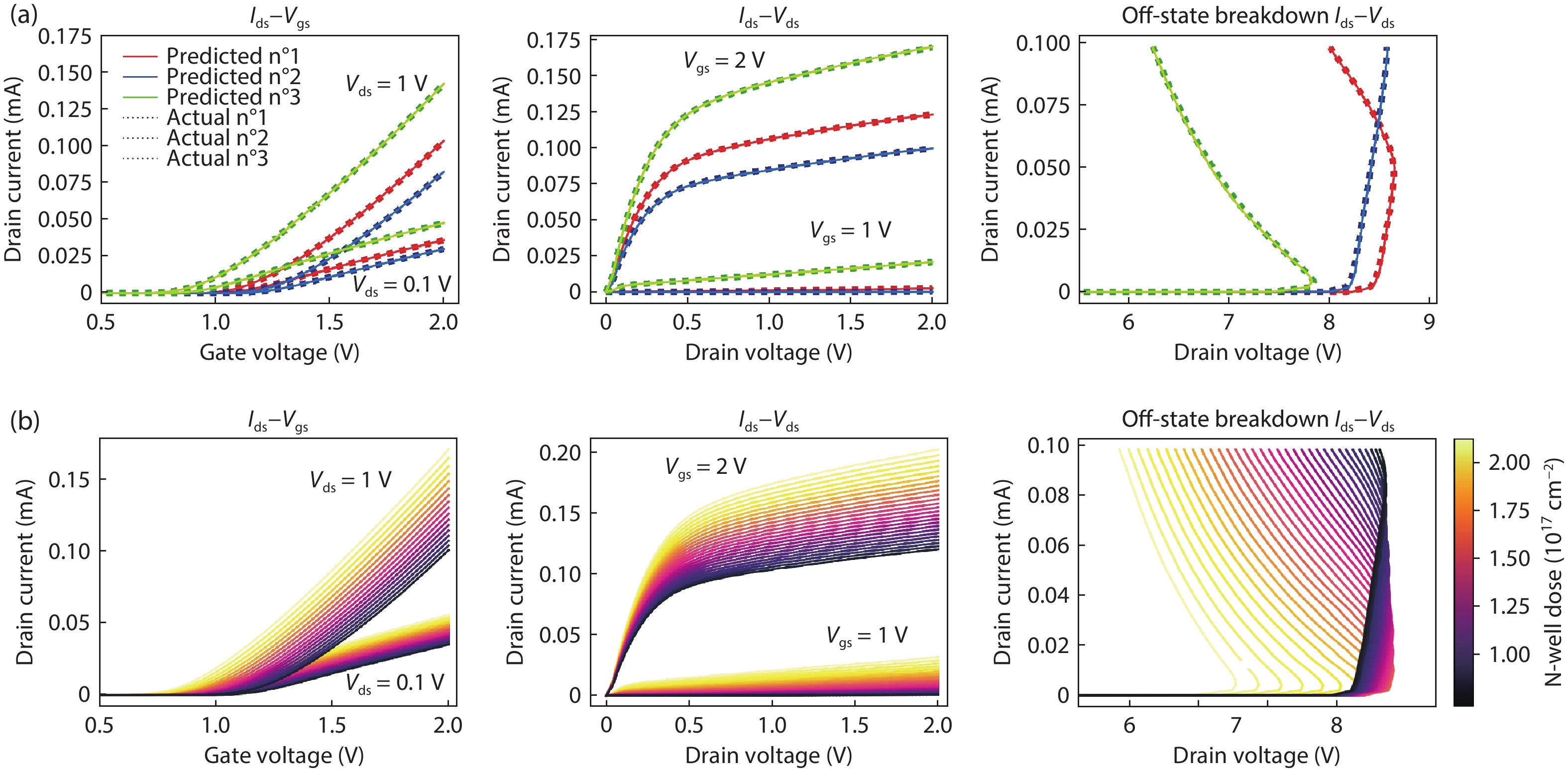
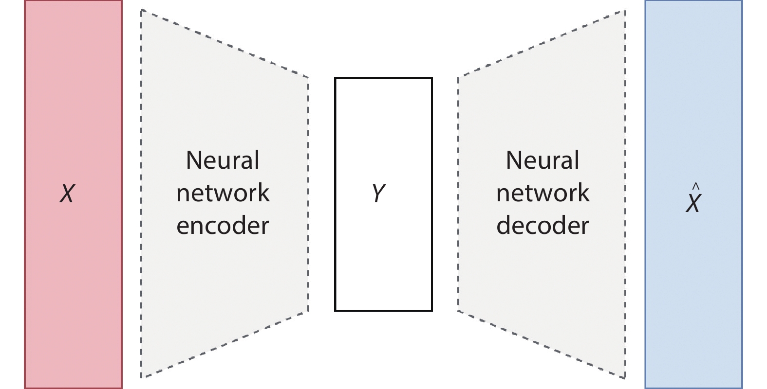
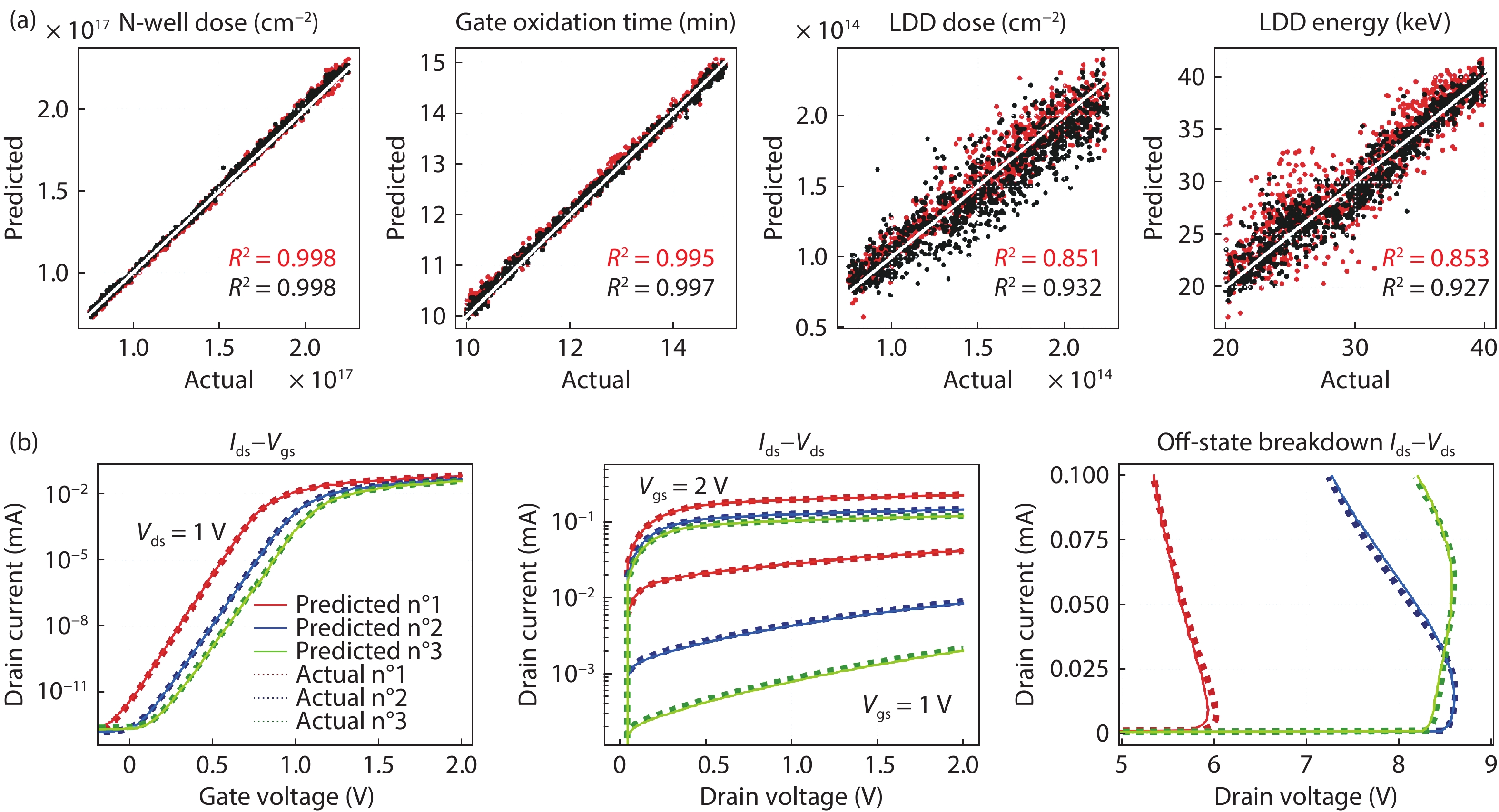
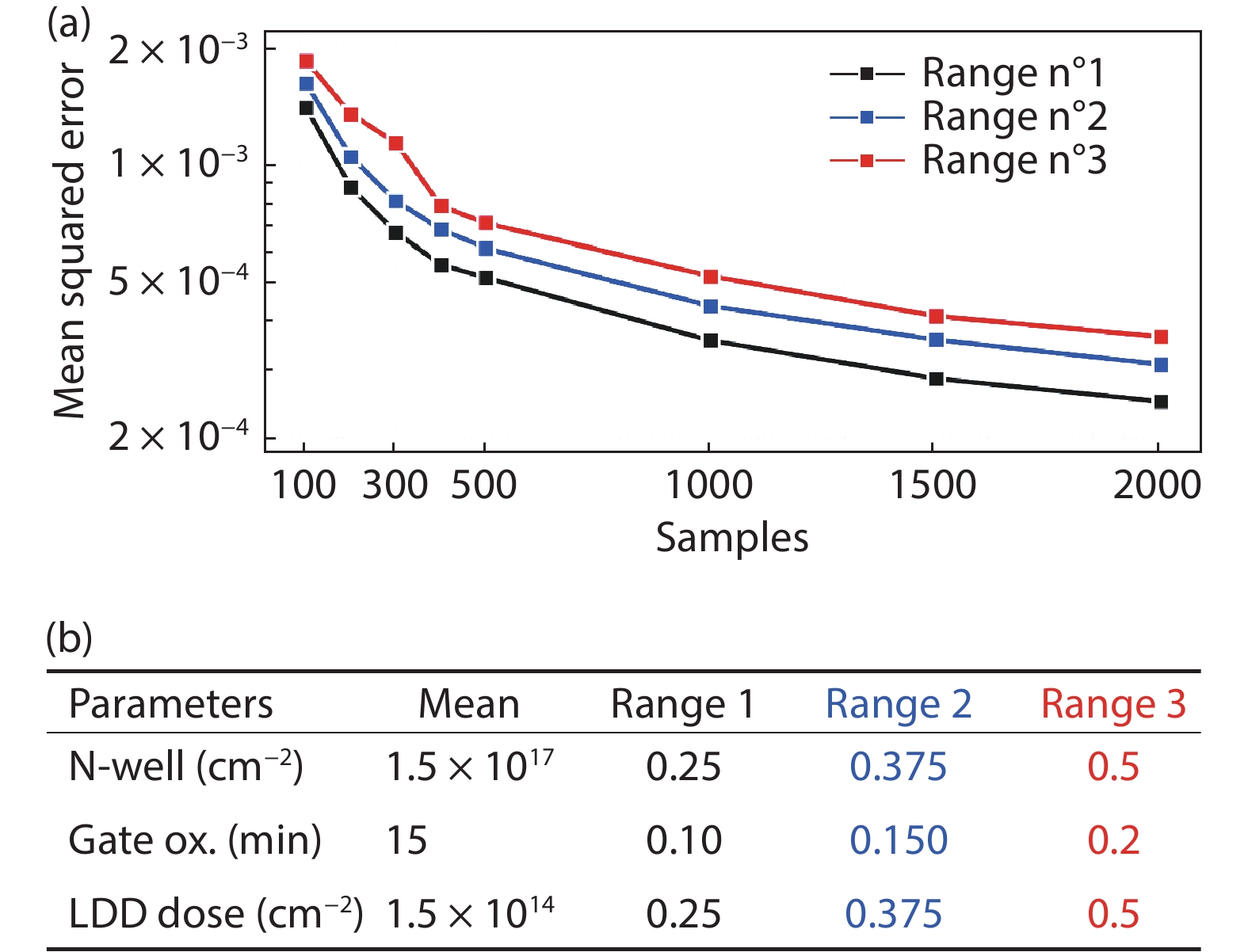
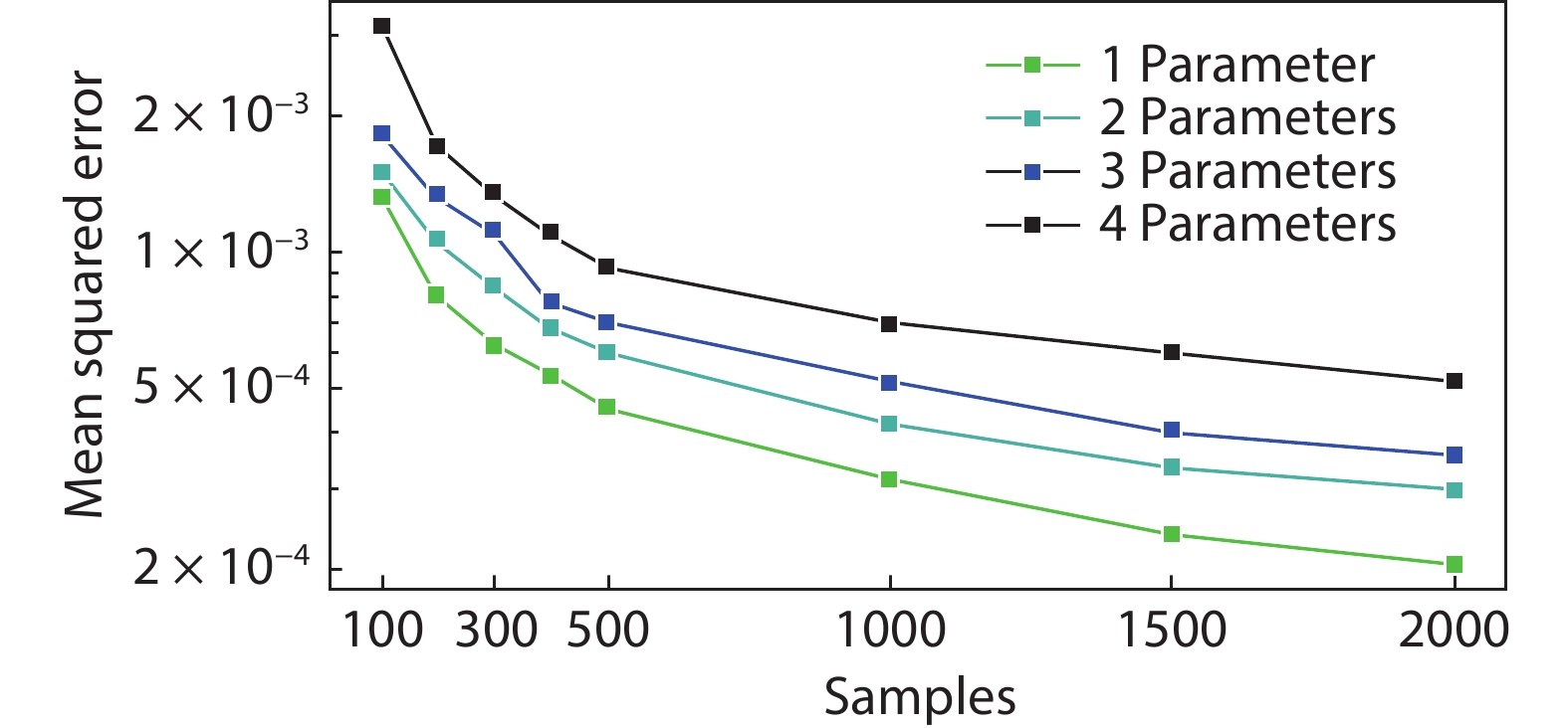
In a world where data is increasingly important for making breakthroughs, microelectronics is a field where data is sparse and hard to acquire. Only a few entities have the infrastructure that is required to automate the fabrication and testing of semiconductor devices. This infrastructure is crucial for generating sufficient data for the use of new information technologies. This situation generates a cleavage between most of the researchers and the industry. To address this issue, this paper will introduce a widely applicable approach for creating custom datasets using simulation tools and parallel computing. The multi-I–V curves that we obtained were processed simultaneously using convolutional neural networks, which gave us the ability to predict a full set of device characteristics with a single inference. We prove the potential of this approach through two concrete examples of useful deep learning models that were trained using the generated data. We believe that this work can act as a bridge between the state-of-the-art of data-driven methods and more classical semiconductor research, such as device engineering, yield engineering or process monitoring. Moreover, this research gives the opportunity to anybody to start experimenting with deep neural networks and machine learning in the field of microelectronics, without the need for expensive experimentation infrastructure.

-01-01.jpg)


