Issue Browser
Volume 42, Issue 4,
Apr 2021

J. Semicond.
2021, 42(4): 041301 doi: 10.1088/1674-4926/42/4/041301

Optical frequency combs have emerged as an important tool enabling diverse applications from test-and-measurement, including spectroscopy, metrology, precision distance measurement, sensing, as well as optical and microwave waveform synthesis, signal processing, and communications. Several techniques exist to generate optical frequency combs, such as mode-locked lasers, Kerr micro-resonators, and electro-optic modulation. Important characteristics of optical frequency combs include the number of comb lines, their spacing, spectral shape and/or flatness, and intensity noise. While mode-locked lasers and Kerr micro-resonators can be used to obtain a large number of comb lines compared to electro-optic modulation, the latter provides increased flexibility in tuning the comb spacing. For some applications in optical communications and microwave photonics, a high degree of integration may be more desirable over a very large number of comb lines. In this paper, we review recent progress on integrated electro-optic frequency comb generators, including those based on indium phosphide, lithium niobate, and silicon photonics.


J. Semicond.
2021, 42(4): 041302 doi: 10.1088/1674-4926/42/4/041302
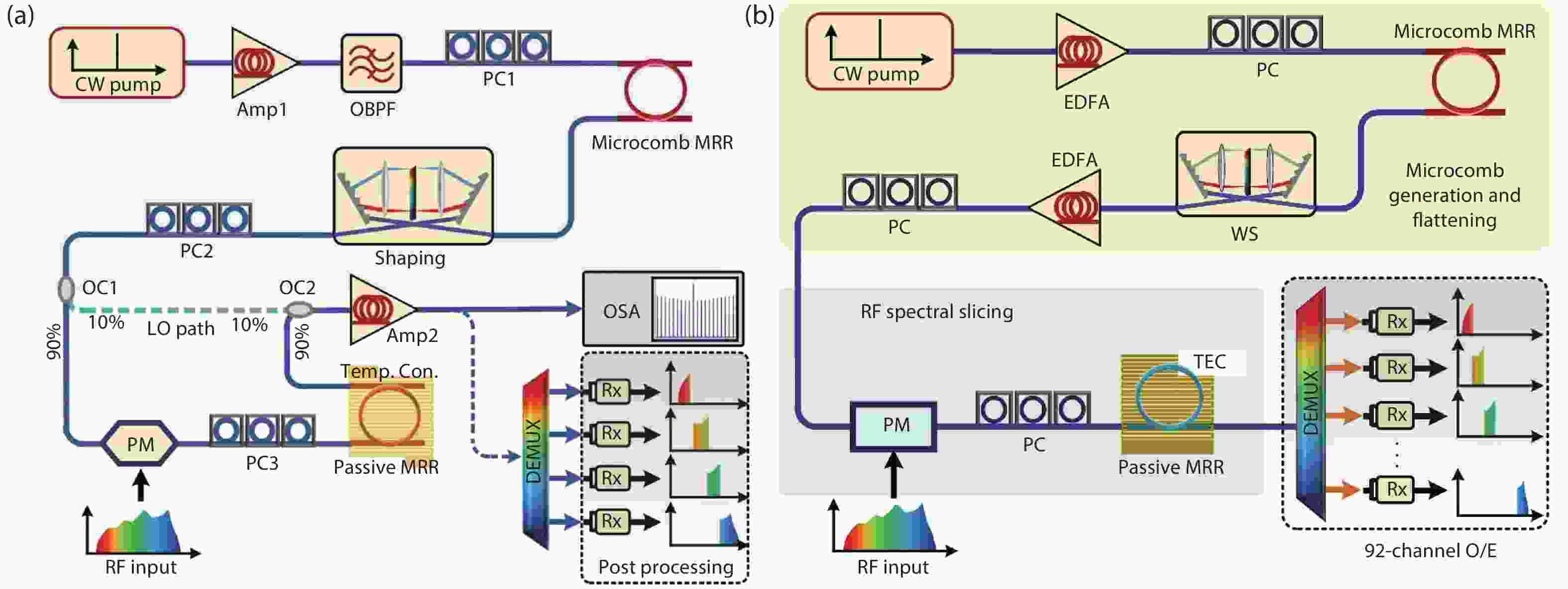
We review recent work on broadband RF channelizers based on integrated optical frequency Kerr micro-combs combined with passive micro-ring resonator filters, with microcombs having channel spacings of 200 and 49 GHz. This approach to realizing RF channelizers offers reduced complexity, size, and potential cost for a wide range of applications to microwave signal detection.


J. Semicond.
2021, 42(4): 041303 doi: 10.1088/1674-4926/42/4/041303
Hybrid integration of III–V and ferroelectric materials is being broadly adopted to enhance functionalities in silicon photonic integrated circuits (PICs). Bonding and transfer printing have been the popular approaches for integration of III–V gain media with silicon PICs. Similar approaches are also being considered for ferroelectrics to enable larger RF modulation bandwidths, higher linearity, lower optical loss integrated optical modulators on chip. In this paper, we review existing integration strategies of III–V materials and present a route towards hybrid integration of both III–V and ferroelectrics on the same chip. We show that adiabatic transformation of the optical mode between hybrid ferroelectric and silicon sections enables efficient transfer of optical modal energies for maximum overlap of the optical mode with the ferroelectric media, similar to approaches adopted to maximize optical overlap with the gain section, thereby reducing lasing thresholds for hybrid III–V integration with silicon PICs. Preliminary designs are presented to enable a foundry compatible hybrid integration route of diverse functionalities on silicon PICs.


J. Semicond.
2021, 42(4): 041304 doi: 10.1088/1674-4926/42/4/041304
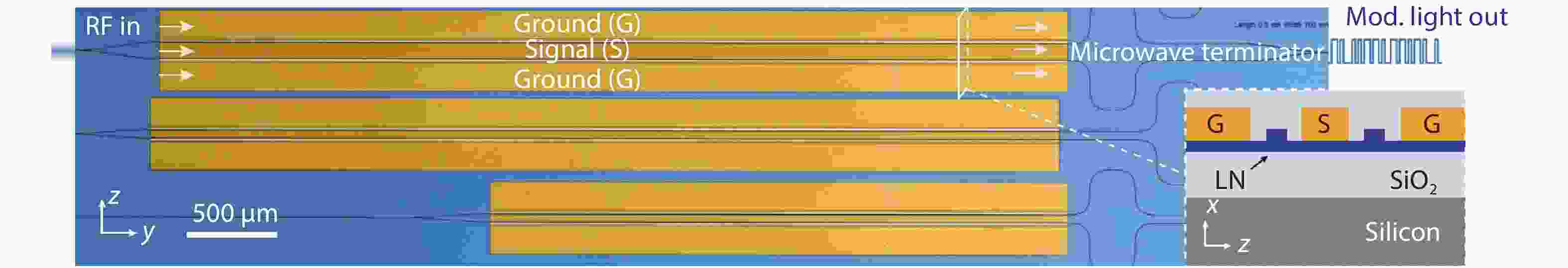
Lithium niobate on insulator (LNOI) is rising as one of the most promising platforms for integrated photonics due to the high-index-contrast and excellent material properties of lithium niobate, such as wideband transparency from visible to mid-infrared, large electro-optic, piezoelectric, and second-order harmonic coefficients. The fast-developing micro- and nano-structuring techniques on LNOI have enabled various structure, devices, systems, and applications. In this contribution, we review the latest developments in this platform, including ultra-high speed electro-optic modulators, optical frequency combs, opto-electro-mechanical system on chip, second-harmonic generation in periodically poled LN waveguides, and efficient edge coupling for LNOI.


J. Semicond.
2021, 42(4): 041305 doi: 10.1088/1674-4926/42/4/041305
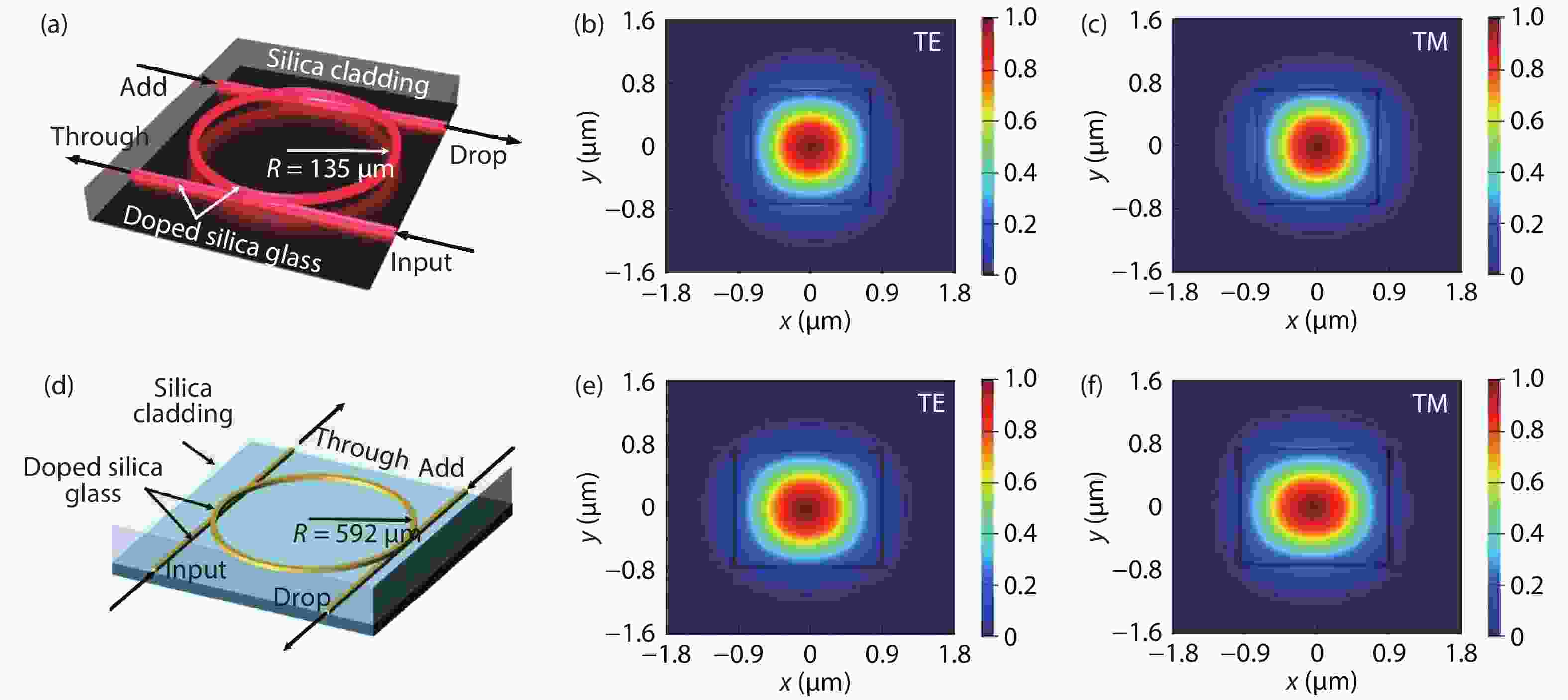
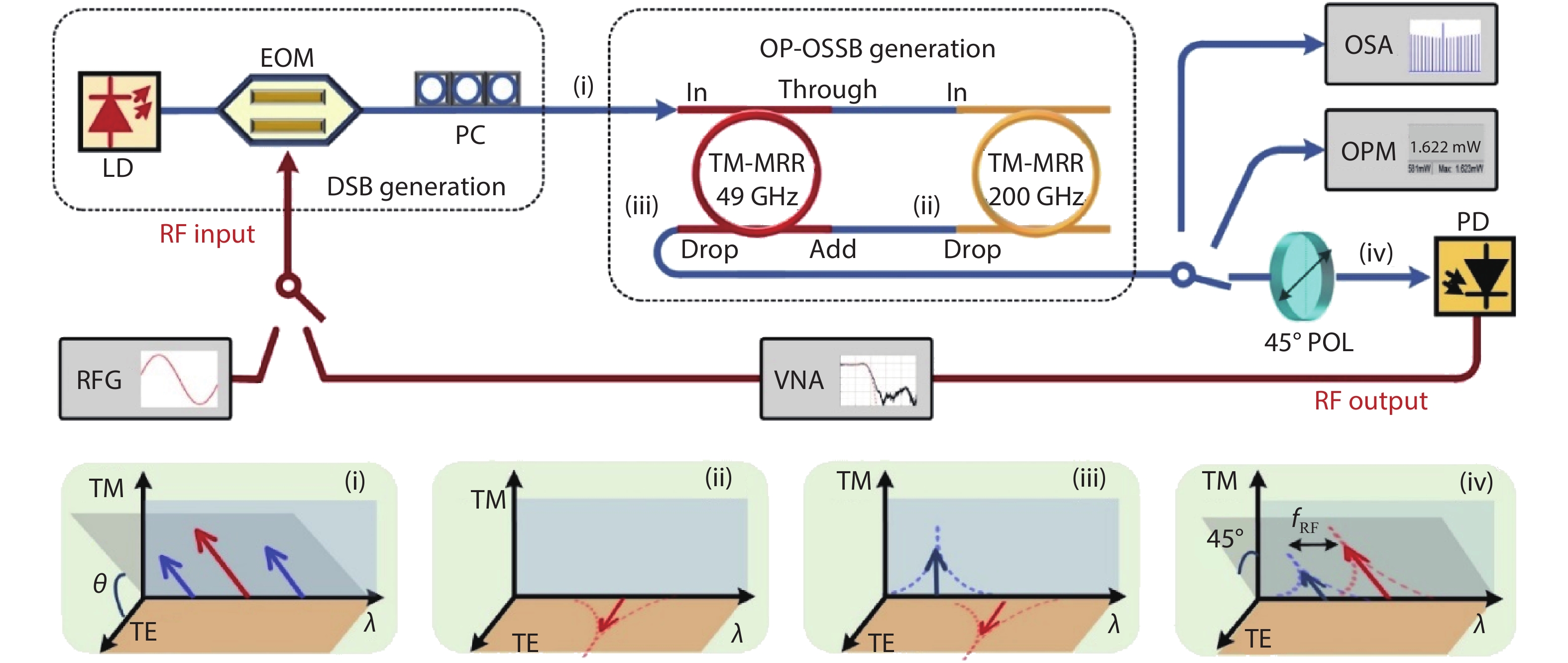
We review recent work on narrowband orthogonally polarized optical RF single sideband generators as well as dual-channel equalization, both based on high-Q integrated ring resonators. The devices operate in the optical telecommunications C-band and enable RF operation over a range of either fixed or thermally tuneable frequencies. They operate via TE/TM mode birefringence in the resonator. We achieve a very large dynamic tuning range of over 55 dB for both the optical carrier-to-sideband ratio and the dual-channel RF equalization for both the fixed and tunable devices.


J. Semicond.
2021, 42(4): 041306 doi: 10.1088/1674-4926/42/4/041306
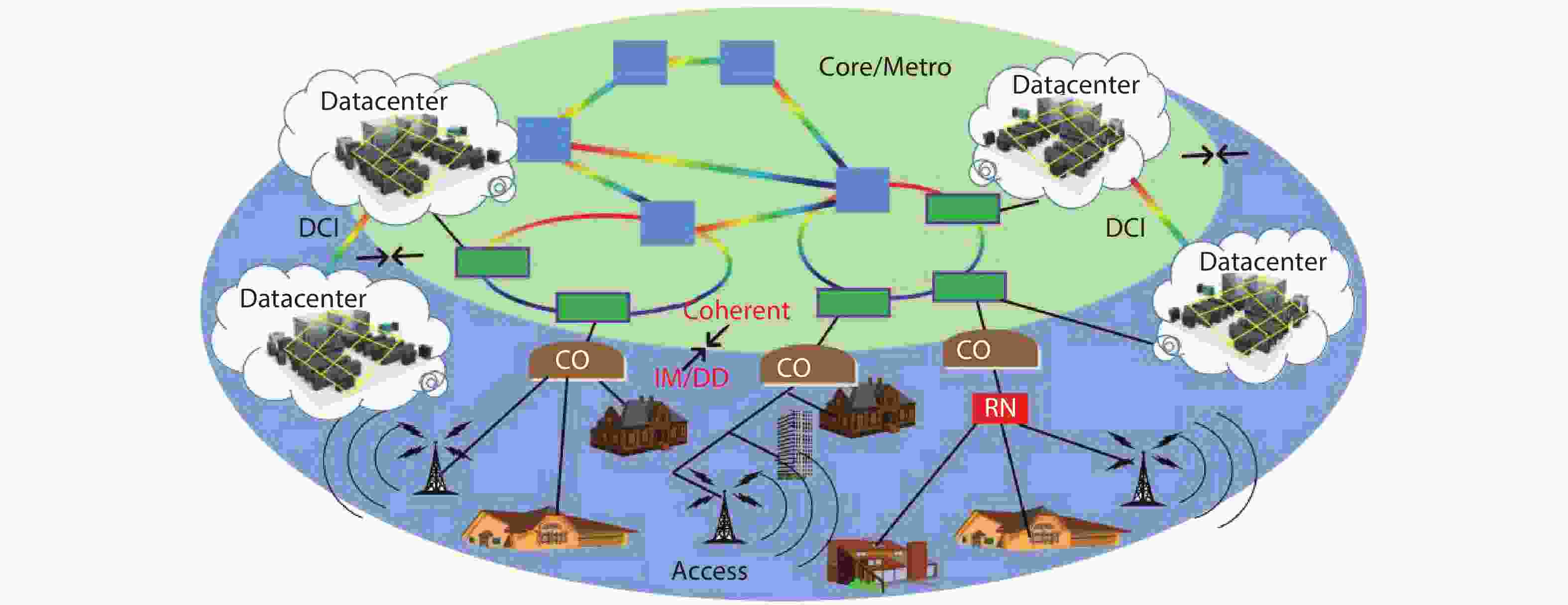
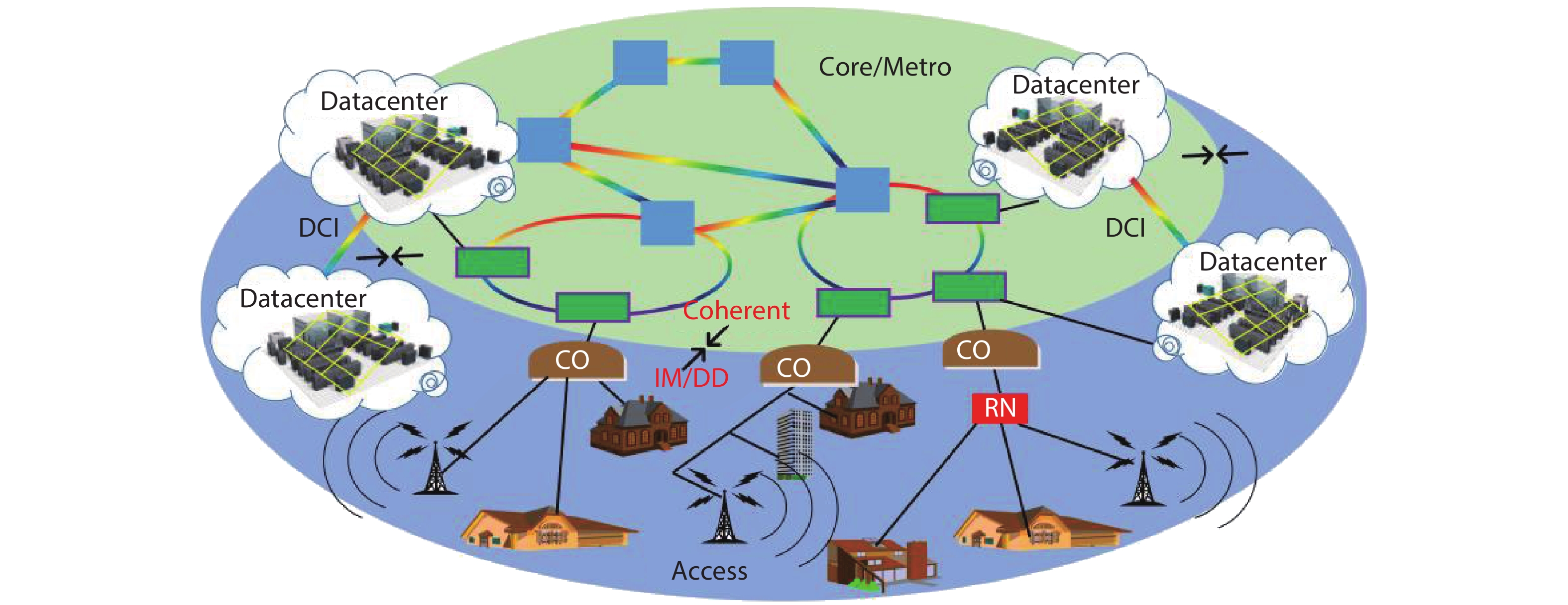
It is very attractive to apply a directly modulated laser (DML)-based intensity-modulation and direct-detection (IM/DD) system in future data centers and 5G fronthaul networks due to the advantages of low cost, low system complexity, and high energy efficiency, which perfectly match the application scenarios of the data centers and 5G fronthaul networks, in which a large number of high-speed optical interconnections are needed. However, as the data traffic in the data centers and 5G fronthaul networks continues to grow exponentially, the future requirements for data rates beyond 100 Gbaud are challenging the existing DML-based IM/DD system, and the main bottleneck is the modulation bandwidth of the DML. In this paper, the data rate demands and technical standards of the data centers and 5G fronthaul networks are reviewed in detail. With the modulation bandwidth requirements, the technical routes and achievements of recent DMLs are reviewed and discussed. In this way, the prospects, challenges, and future development of DMLs in the applications of future data centers and 5G fronthaul networks are comprehensively explored.


J. Semicond.
2021, 42(4): 041307 doi: 10.1088/1674-4926/42/4/041307

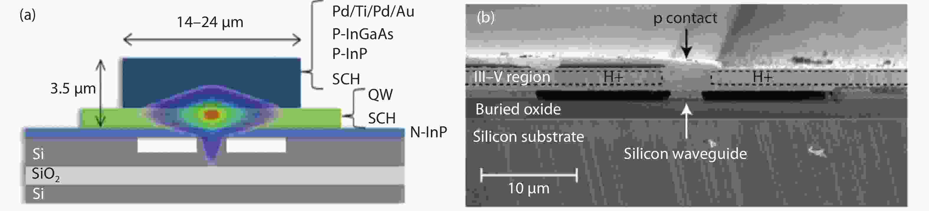
Efficient light generation and amplification has long been missing on the silicon platform due to its well-known indirect bandgap nature. Driven by the size, weight, power and cost (SWaP-C) requirements, the desire to fully realize integrated silicon electronic and photonic integrated circuits has greatly pushed the effort of realizing high performance on-chip lasers and amplifiers moving forward. Several approaches have been proposed and demonstrated to address this issue. In this paper, a brief overview of recent progress of the high-performance lasers and amplifiers on Si based on different technology is presented. Representative device demonstrations, including ultra-narrow linewidth III–V/Si lasers, fully integrated III–V/Si/Si3N4 lasers, high-channel count mode locked quantum dot (QD) lasers, and high gain QD amplifiers will be covered.


J. Semicond.
2021, 42(4): 041308 doi: 10.1088/1674-4926/42/4/041308
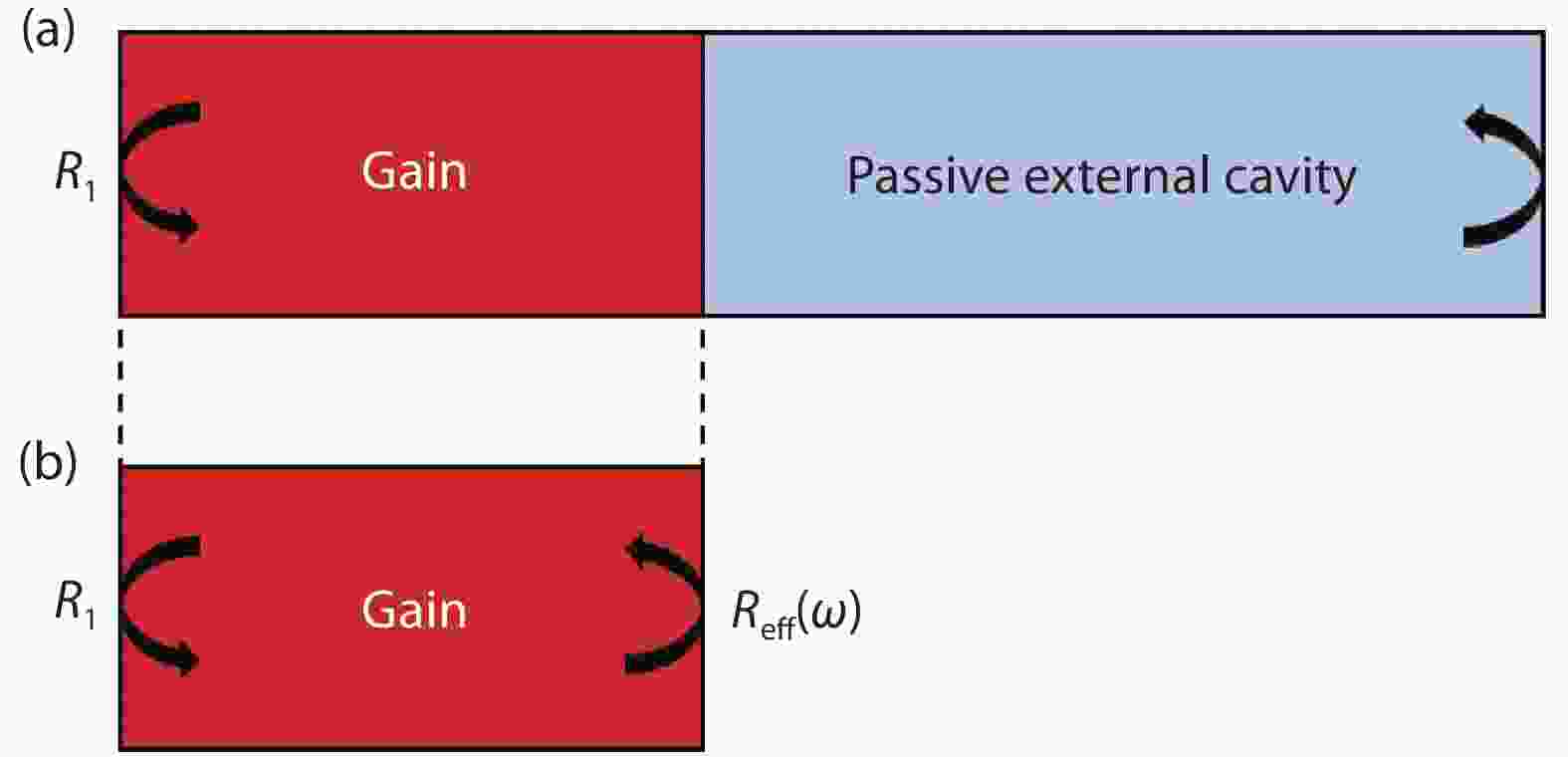
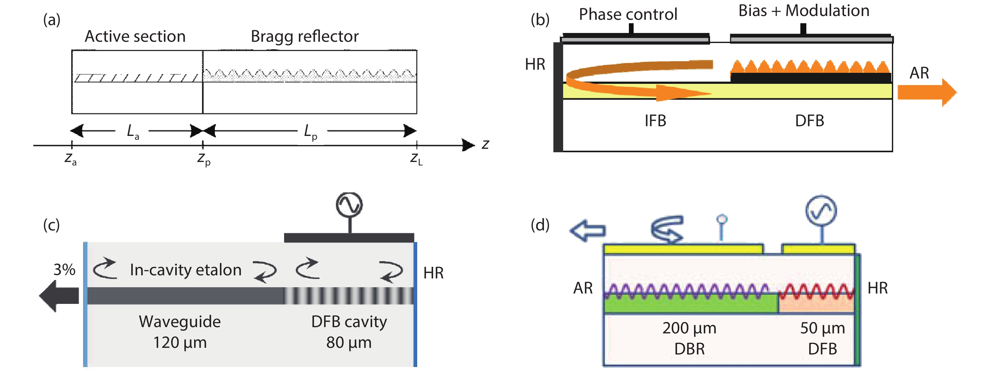
Narrow linewidth light source is a prerequisite for high-performance coherent optical communication and sensing. Waveguide-based external cavity narrow linewidth semiconductor lasers (WEC-NLSLs) have become a competitive and attractive candidate for many coherent applications due to their small size, volume, low energy consumption, low cost and the ability to integrate with other optical components. In this paper, we present an overview of WEC-NLSLs from their required technologies to the state-of-the-art progress. Moreover, we highlight the common problems occurring to current WEC-NLSLs and show the possible approaches to resolving the issues. Finally, we present the possible development directions for the next phase and hope this review will be beneficial to the advancements of WEC-NLSLs.


J. Semicond.
2021, 42(4): 042301 doi: 10.1088/1674-4926/42/4/042301
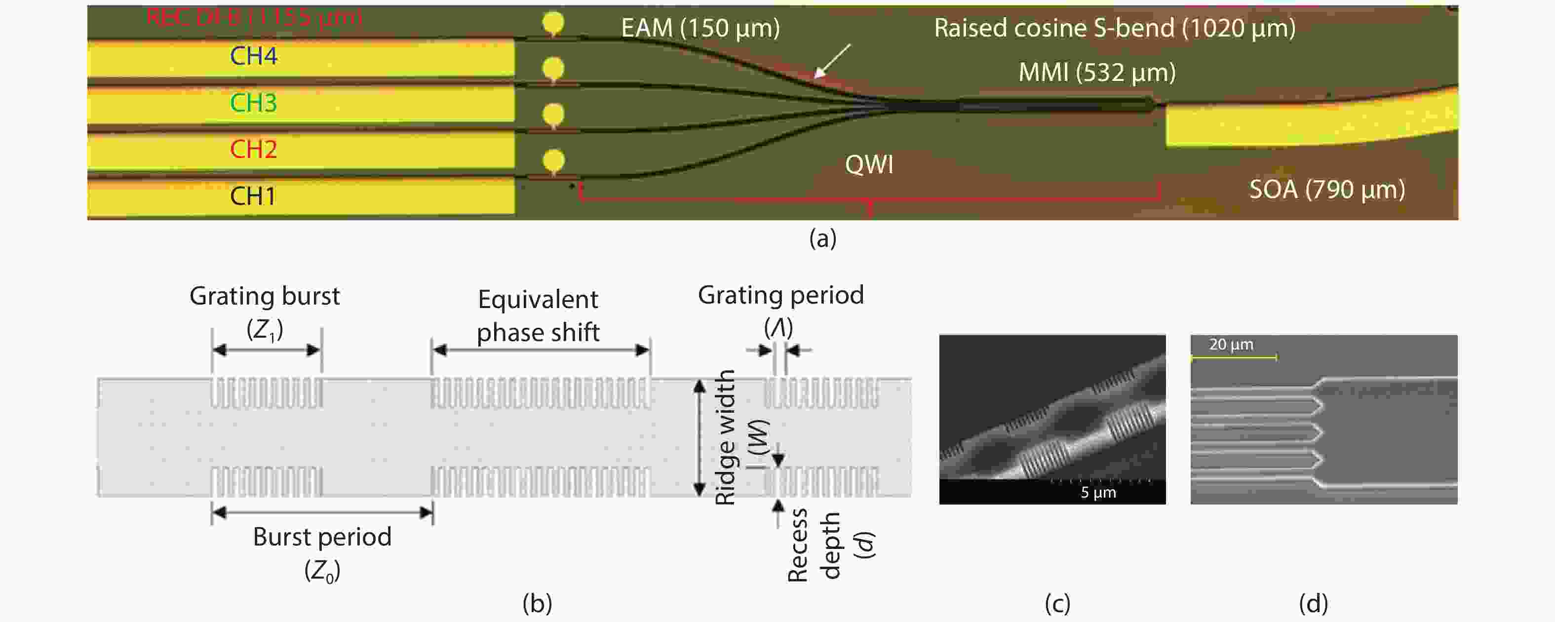
We report a low-cost manufacturing approach for fabricating monolithic multi-wavelength sources for dense wavelength division multiplexing (DWDM) systems that offers high yield and eliminates crystal regrowth and selective area epitaxy steps that are essential in traditional fabrication methods. The source integrates an array of distributed feedback (DFB) lasers with a passive coupler and semiconductor optical amplifier (SOA). Ridge waveguide lasers with sampled Bragg side wall gratings have been integrated using quantum well intermixing to achieve a fully functional four-channel DWDM source with 0.8 nm wavelength spacing and residual errors < 0.13 nm. The output power from the SOA is > 10 mW per channel making the source suitable for use in passive optical networks (PONs). We have also investigated using multisection phase-shifted sampled gratings to both increase the effective grating coupling coefficient and precisely control the channel lasing wavelength spacing. An 8-channel DFB laser array with 100 GHz channel spacing was demonstrated using a sampled grating with two π-phase-shifted sections in each sampling period. The entire array was fabricated by only a single step of electron beam lithography.


J. Semicond.
2021, 42(4): 042302 doi: 10.1088/1674-4926/42/4/042302

A nonlinear integrated optical platform that allows the fabrication of waveguide circuits with different material composition, and at small dimensions, offers advantages in terms of field enhancement and increased interaction length, thereby facilitating the observation of nonlinear optics effects at a much lower power level. To enhance the nonlinearity of the conventional waveguide structure, in this work, we propose and demonstrate a microstructured waveguide where silicon rich layer is embedded in the core of the conventional waveguide in order to increase its nonlinearity. By embedding a 20 nm thin film of silicon nanocrystal (Si-nc), we achieve a twofold increase of the nonlinear parameter, γ. The linear relationship between the four-wave mixing conversion efficiency and pump power reveals the negligible nonlinear absorption and small dispersion in the micro-ring resonators. This simple approach of embedding an ultra-thin Si-nc layer into conventional high-index doped silica dramatically increases its nonlinear performance, and could potentially find applications in all-optical processing functions.


J. Semicond.
2021, 42(4): 042303 doi: 10.1088/1674-4926/42/4/042303
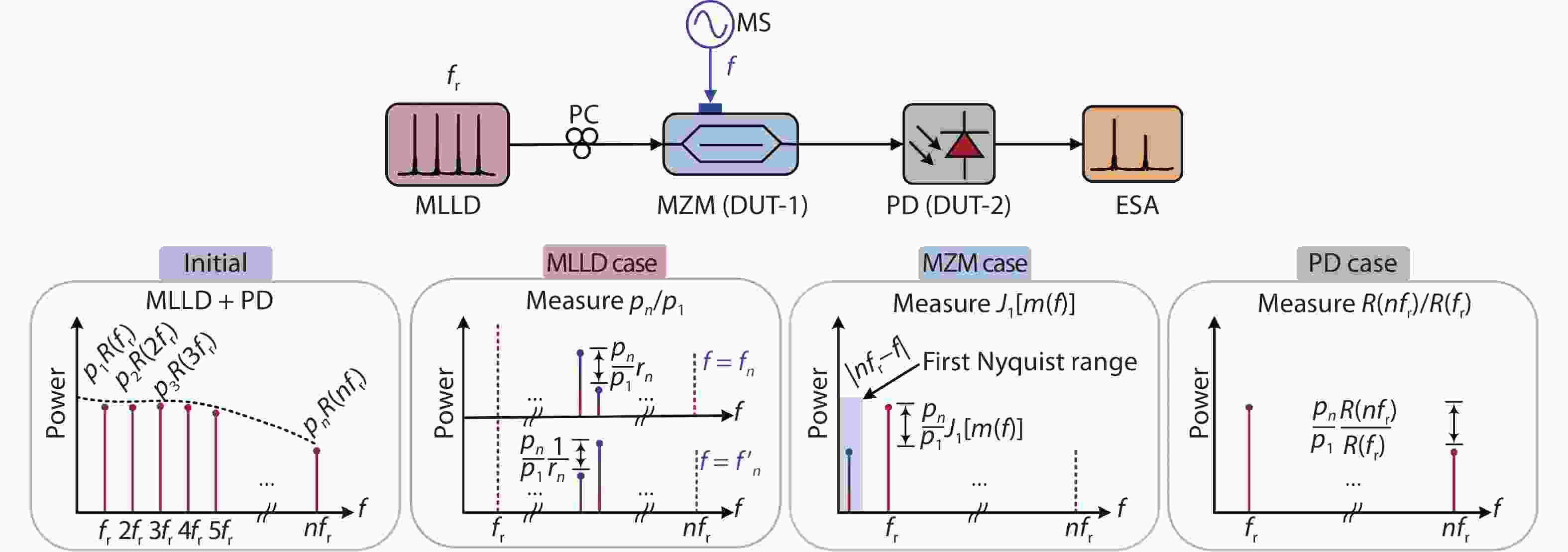
We propose a low-speed photonic sampling for independent high-frequency characterization of a Mach–Zehnder modulator (MZM) and a photodetector (PD) in an optical link. A low-speed mode-locked laser diode (MLLD) provides an ultra-wideband optical stimulus with scalable frequency range, working as the photonic sampling source of the link. The uneven spectrum lines of the MLLD are firstly characterized with symmetric modulation within the interesting frequency range. Then, the electro-optic modulated signals are down-converted to the first Nyquist frequency range, yielding the self-referenced extraction of modulation depth and half-wave voltage of the MZM without correcting the responsivity fluctuation of the PD in the link. Finally, the frequency responsivity of the PD is self-referenced measured under null modulation of the MZM. As frequency responses of the MZM and the PD can be independently obtained, our method allows self-referenced high-frequency measurement for a high-speed optical link. In the proof-of-concept experiment, a 96.9 MS/s MLLD is used for measuring a MZM and a PD within the frequency range up to 50 GHz. The consistency between our method and the conventional method verifies that the ultra-wideband and self-referenced high-frequency characterization of high-speed MZMs and PDs.