Issue Browser
Volume 42, Issue 3,
Mar 2021


J. Semicond.
2021, 42(3): 031101 doi: 10.1088/1674-4926/42/3/031101

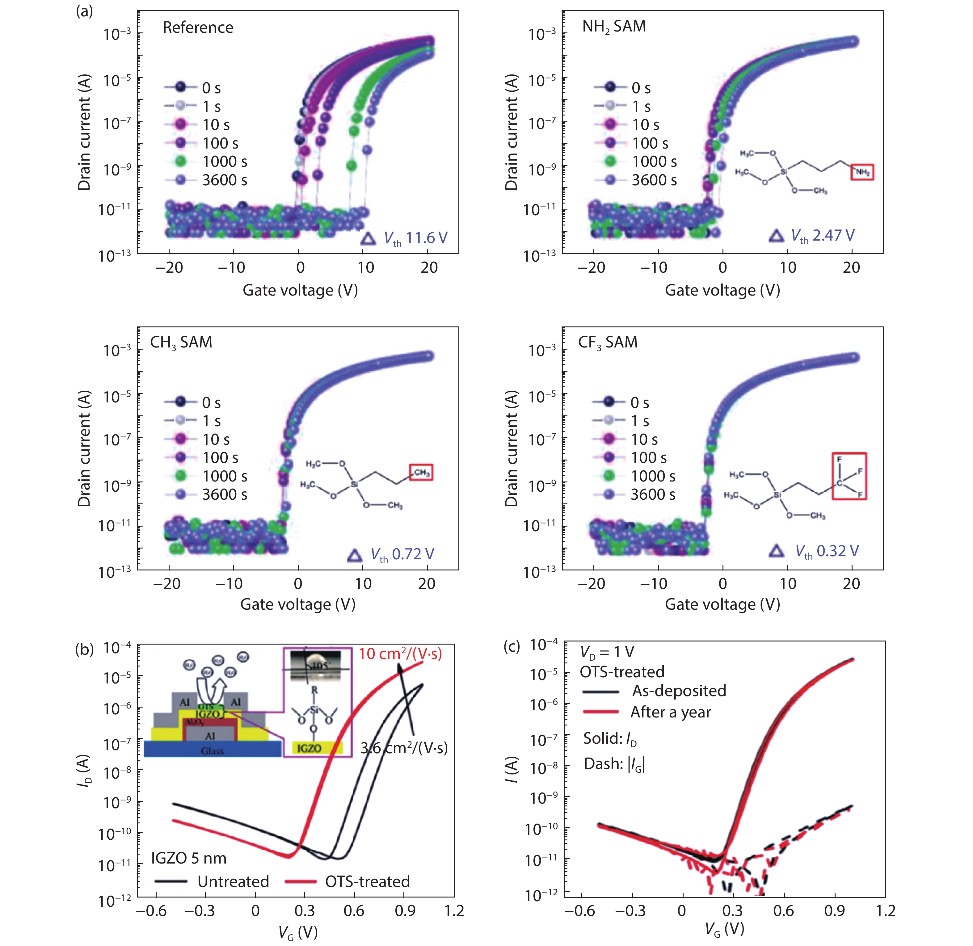
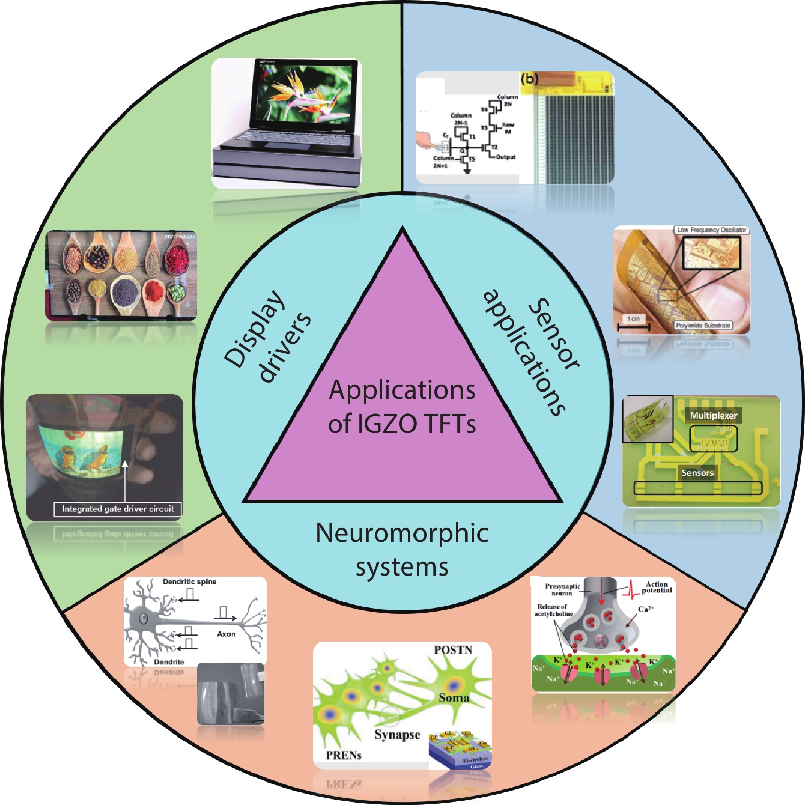
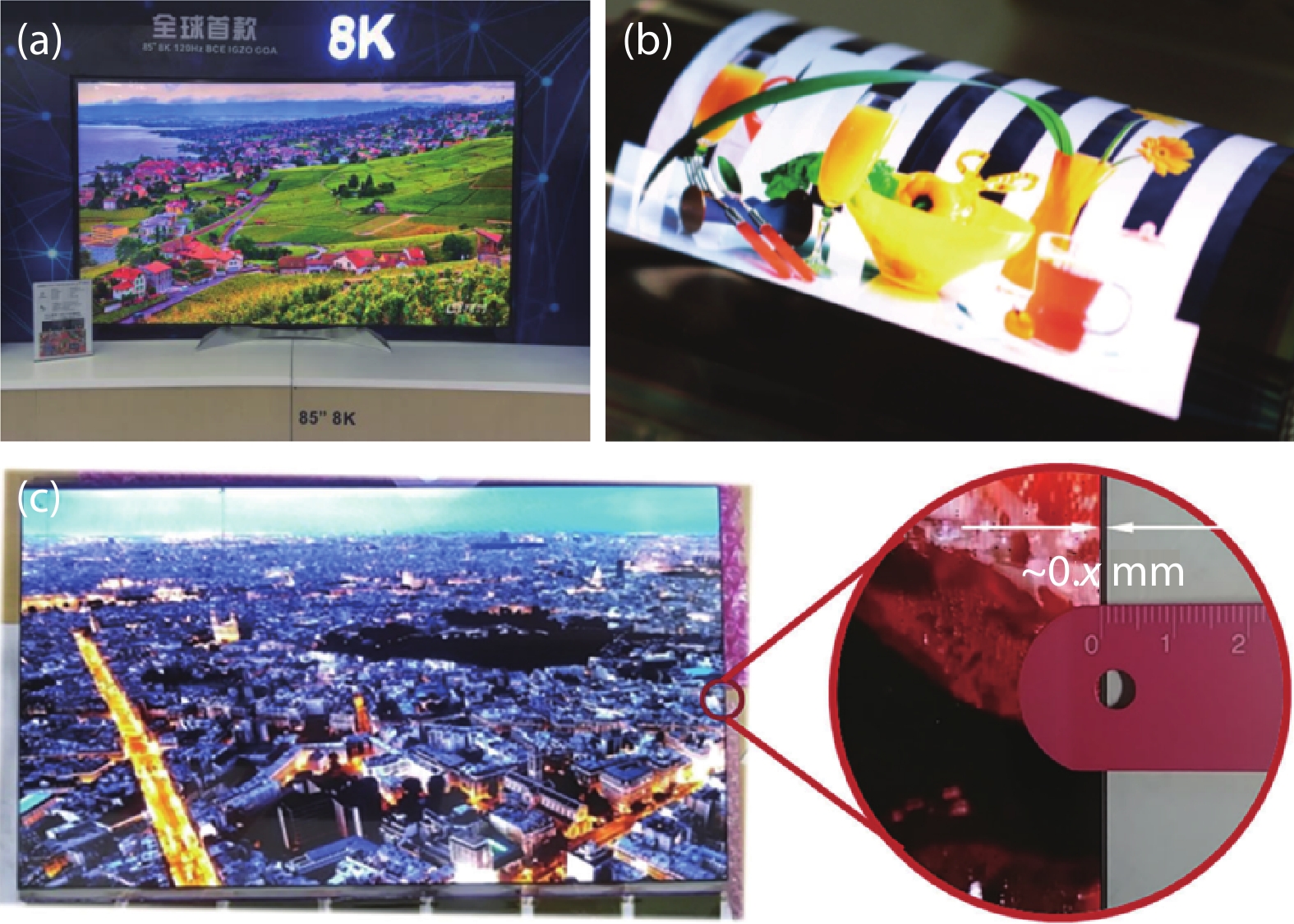
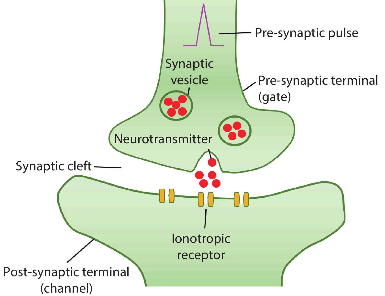
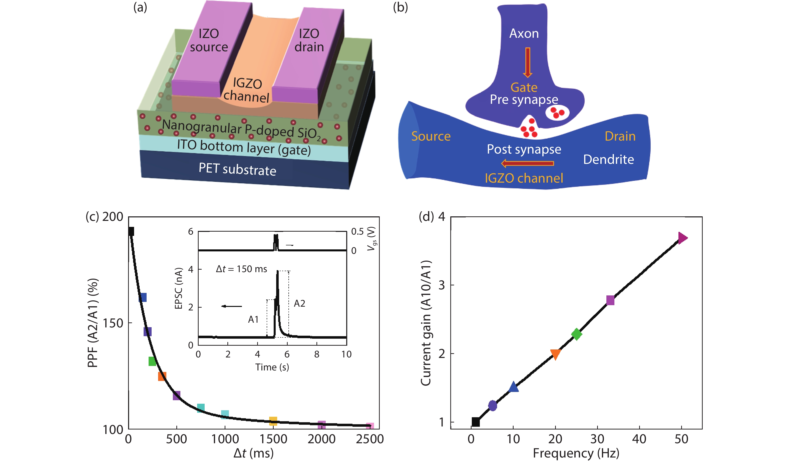
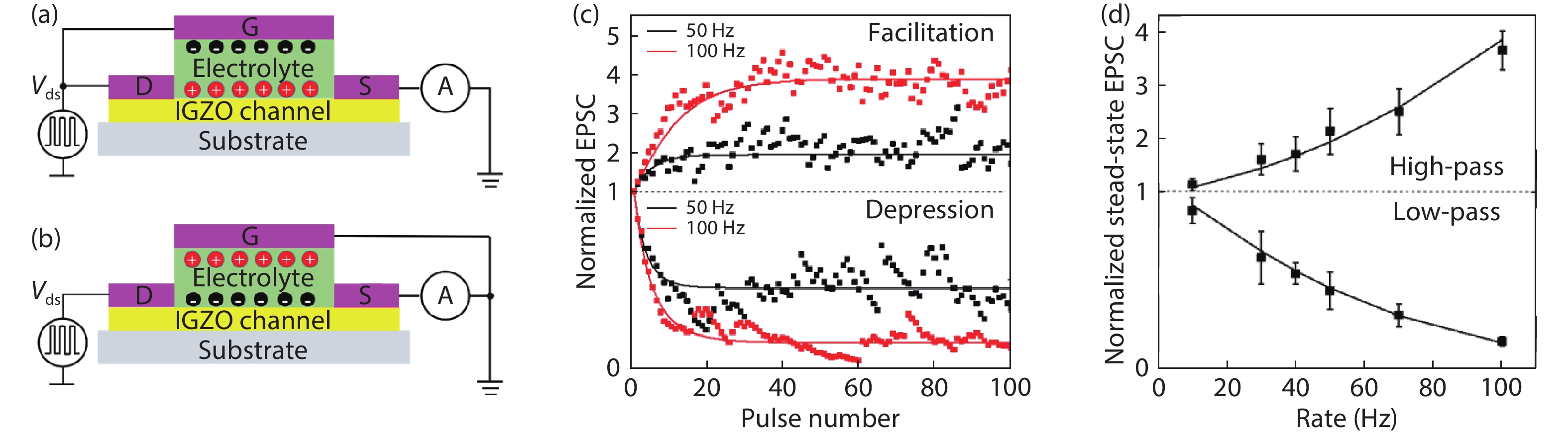
Since the invention of amorphous indium–gallium–zinc–oxide (IGZO) based thin-film transistors (TFTs) by Hideo Hosono in 2004, investigations on the topic of IGZO TFTs have been rapidly expanded thanks to their high electrical performance, large-area uniformity, and low processing temperature. This article reviews the recent progress and major trends in the field of IGZO-based TFTs. After a brief introduction of the history of IGZO and the main advantages of IGZO-based TFTs, an overview of IGZO materials and IGZO-based TFTs is given. In this part, IGZO material electron travelling orbitals and deposition methods are introduced, and the specific device structures and electrical performance are also presented. Afterwards, the recent advances of IGZO-based TFT applications are summarized, including flat panel display drivers, novel sensors, and emerging neuromorphic systems. In particular, the realization of flexible electronic systems is discussed. The last part of this review consists of the conclusions and gives an outlook over the field with a prediction for the future.


J. Semicond.
2021, 42(3): 031701 doi: 10.1088/1674-4926/42/3/031701

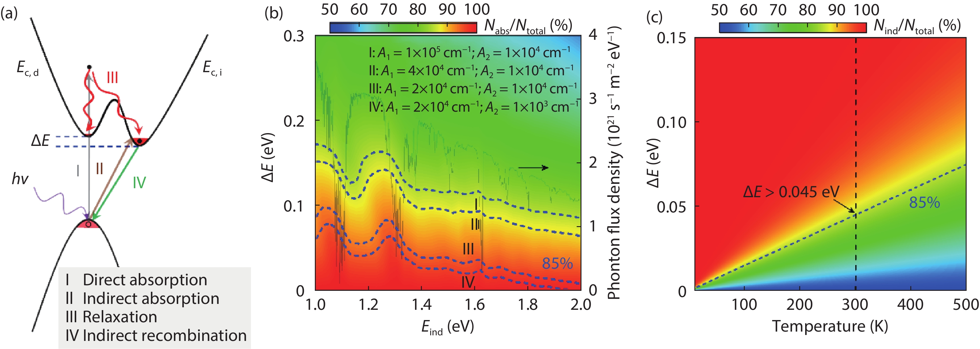
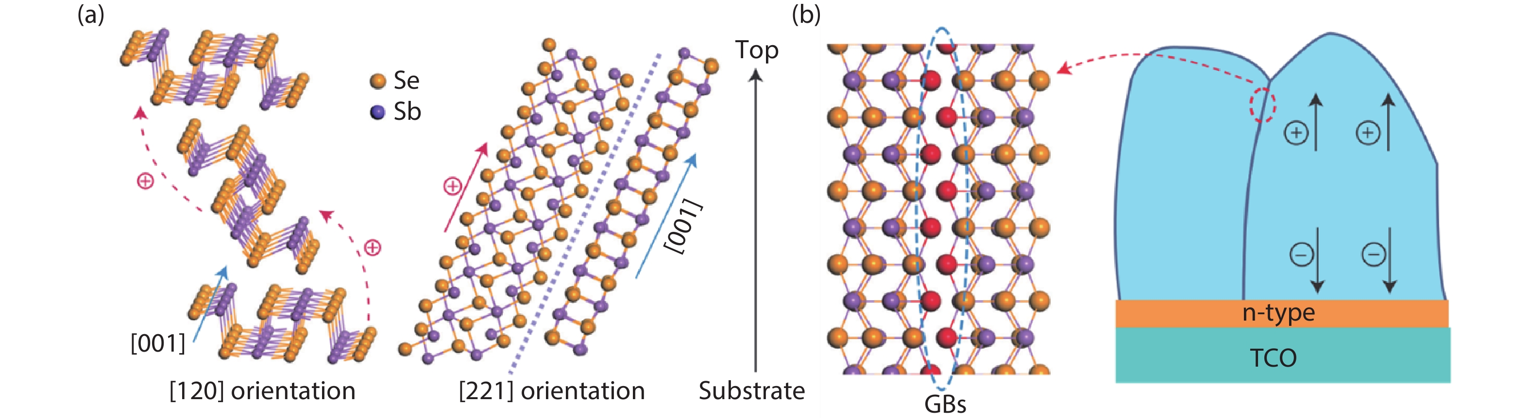
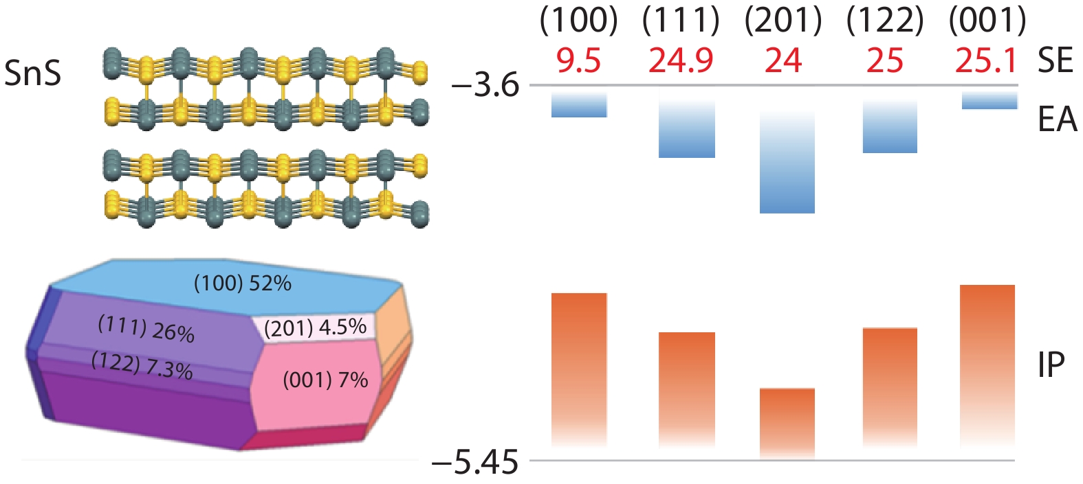
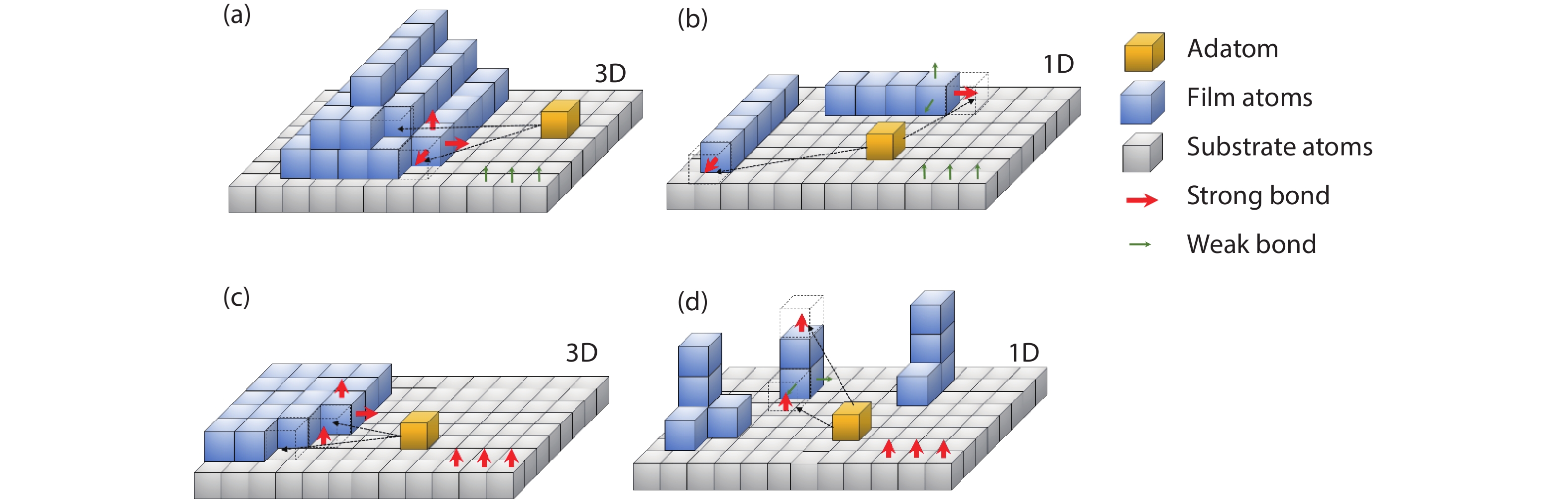
The photovoltaic (PV) market is currently dominated by silicon based solar cells. However technological diversification is essential to promote competition, which is the driving force for technological growth. Historically, the choice of PV materials has been limited to the three-dimensional (3D) compounds with a high crystal symmetry and direct band gap. However, to meet the strict demands for sustainable PV applications, material space has been expanded beyond 3D compounds. In this perspective we discuss the potential of low-dimensional materials (2D, 1D) for application in PVs. We present unique features of low-dimensional materials in context of their suitability in the solar cells. The band gap, absorption, carrier dynamics, mobility, defects, surface states and growth kinetics are discussed and compared to 3D counterparts, providing a comprehensive view of prospects of low-dimensional materials. Structural dimensionality leads to a highly anisotropic carrier transport, complex defect chemistry and peculiar growth dynamics. By providing fundamental insights into these challenges we aim to deepen the understanding of low-dimensional materials and expand the scope of their application. Finally, we discuss the current research status and development trend of solar cell devices made of low-dimensional materials.


J. Semicond.
2021, 42(3): 032001 doi: 10.1088/1674-4926/42/3/032001
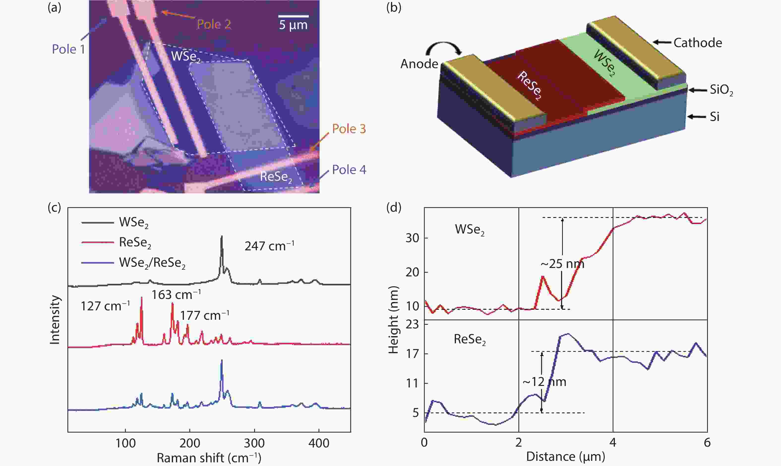
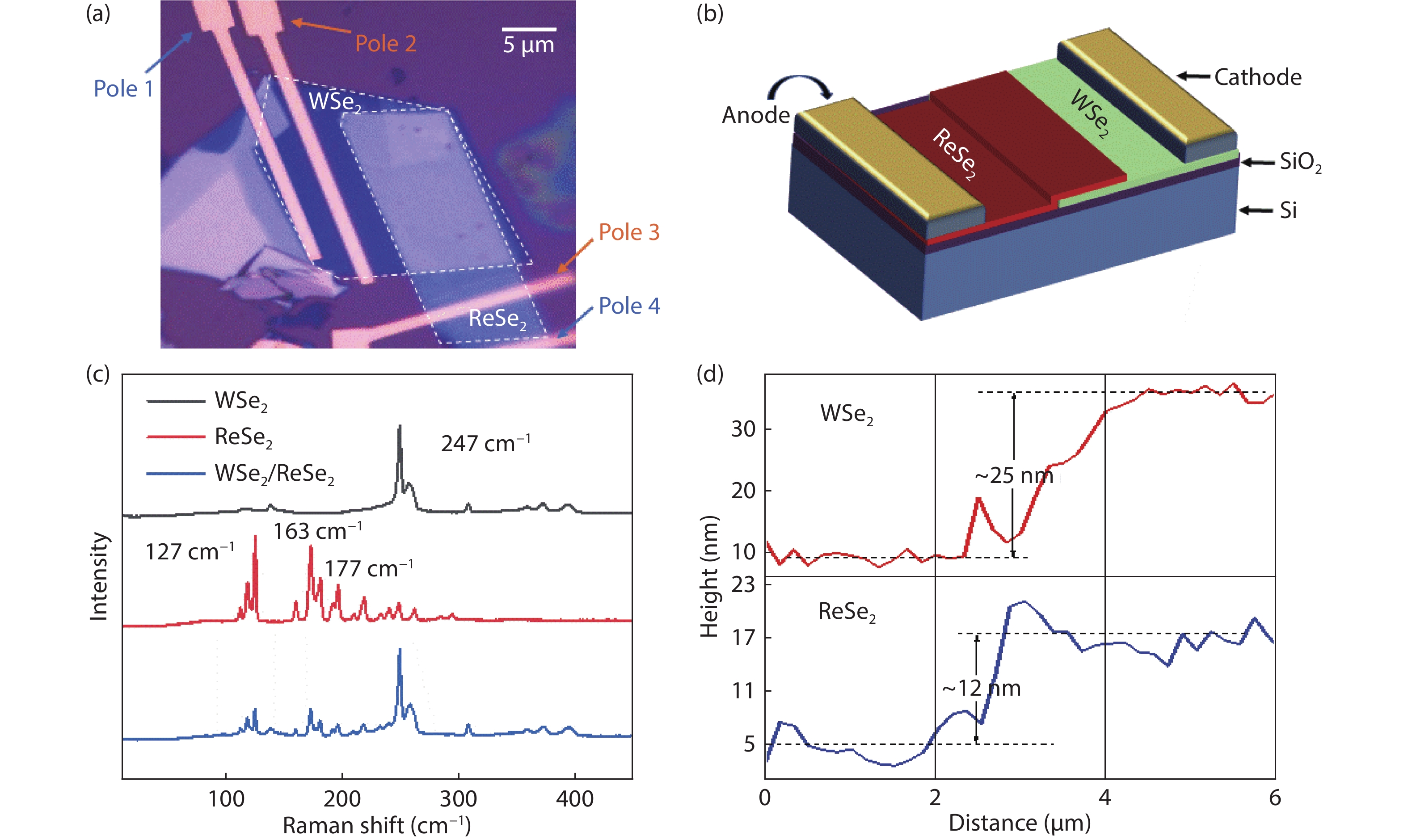
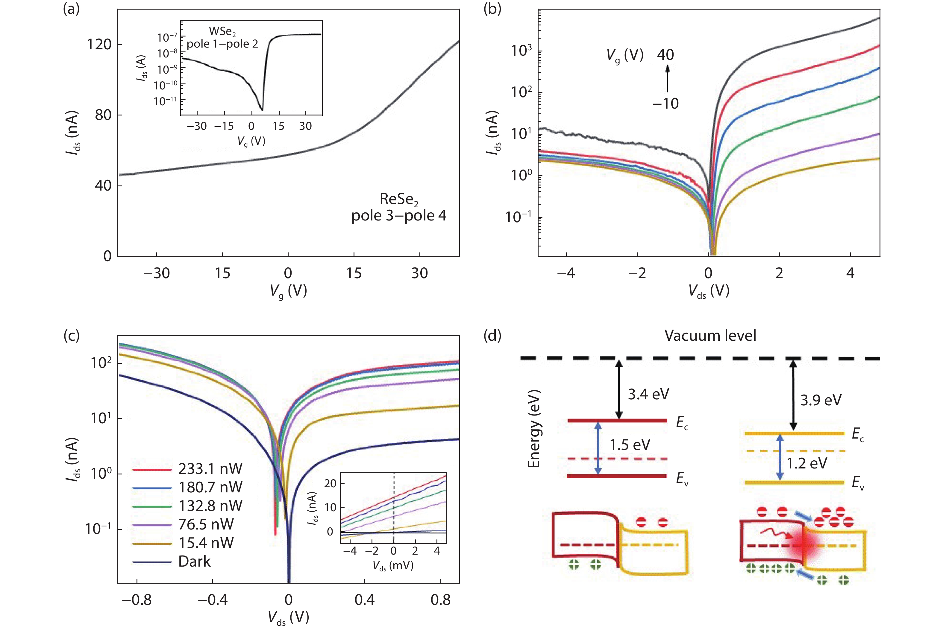
Polarization-resolved photodetectors, a significant branch of photodetection, can more effectively distinguish the target from the background by exploiting polarization-sensitive characteristics. However, due to the absence of intrinsic polarized absorption properties of many materials, there is still a great challenge to develop the high-performance polarization-resolved photodetectors. Here, we report a van der Waals heterojunction (vdWH) ReSe2/WSe2 photodetector, which performs a high responsivity of ~0.28 A/W and a high detectivity of 1.1 × 10¹² Jones under the illumination of 520 nm laser at room temperature. Remarkably, scanning photocurrent mapping (SPCM) measurements demonstrate the photoresponse of devices closely depend on the polarized angle of the incident light, indicating the effective polarized light detection. This work paves the way to develop high-performance polarization-resolved photodetectors based on two-dimensional (2D) materials.


J. Semicond.
2021, 42(3): 032101 doi: 10.1088/1674-4926/42/3/032101

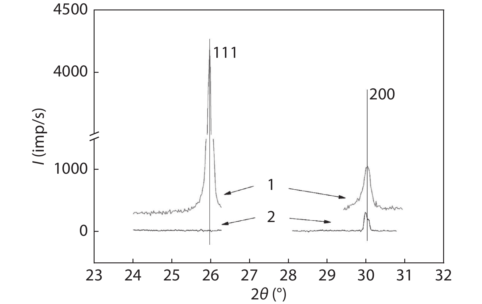
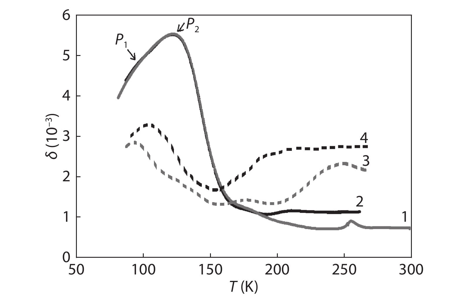
In this paper, the dependencies of Young's modulus and attenuation decrement on samarium sulfide polycrystals (SmS) under various annealing temperatures are studied by the piezoelectric ultrasonic composite oscillator technique at a frequency of 100 kHz in the temperature range of 80–300 K. A decrease in Young's modulus with an increase of the annealing temperature due to the texturing of the material was revealed. At the same time, attenuation peaks were observed at temperatures about 90 and 125 K, presumably due to Niblett-Wilks and Bordoni relaxations.

J. Semicond.
2021, 42(3): 032401 doi: 10.1088/1674-4926/42/3/032401
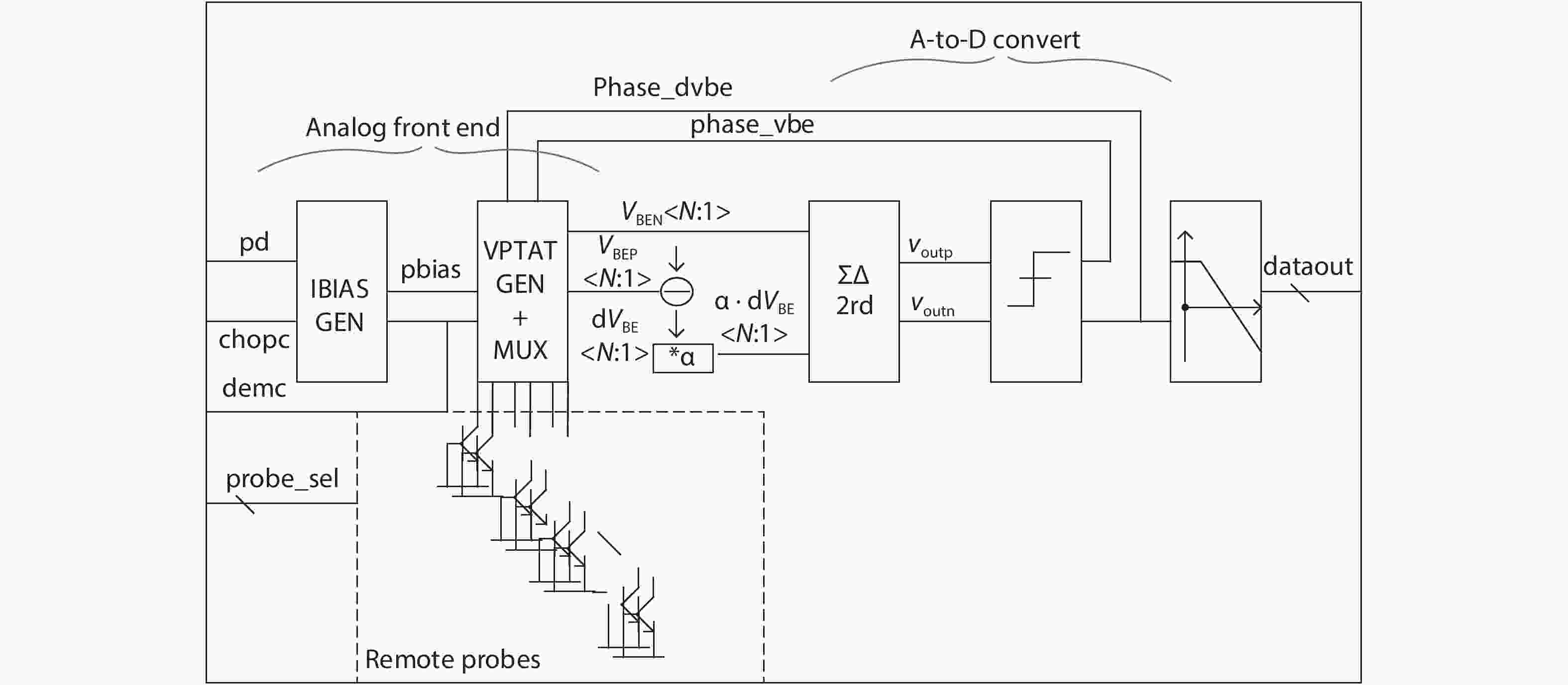
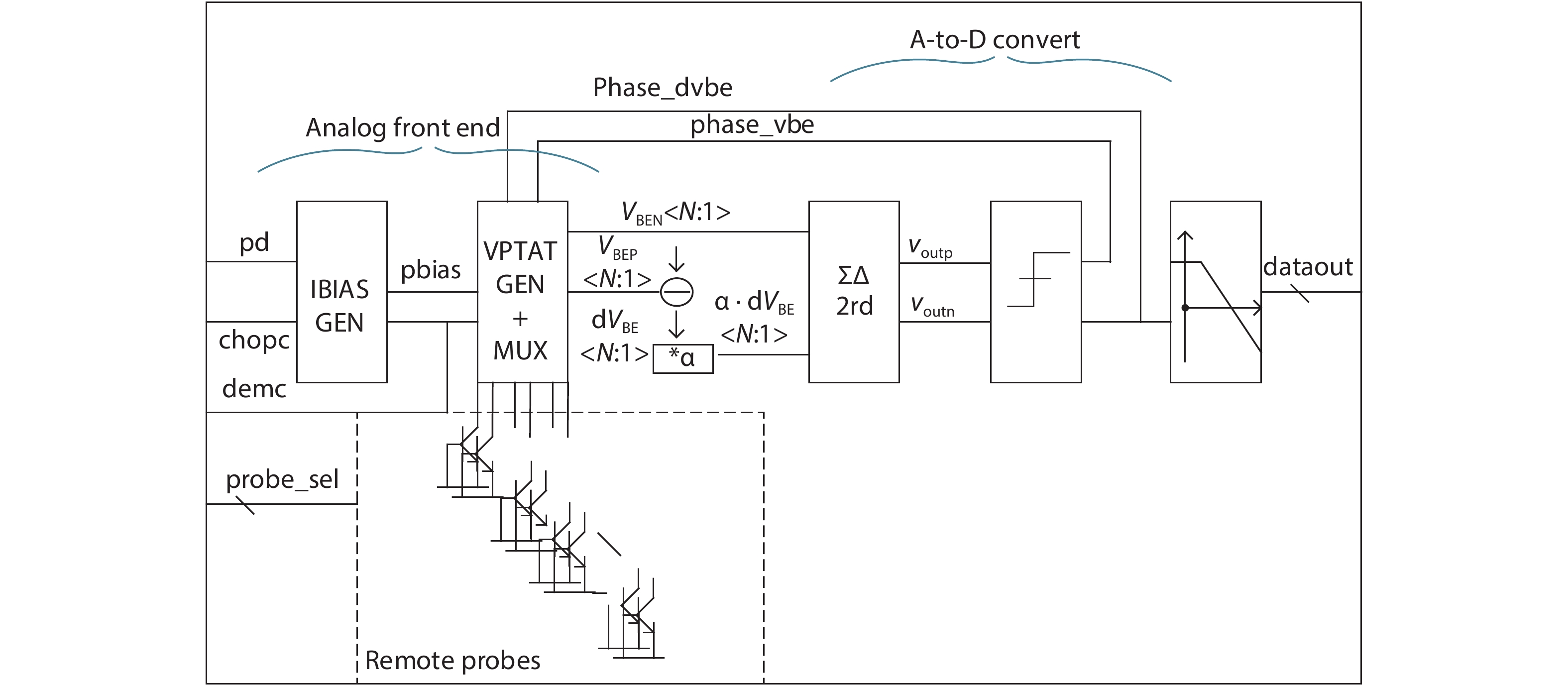
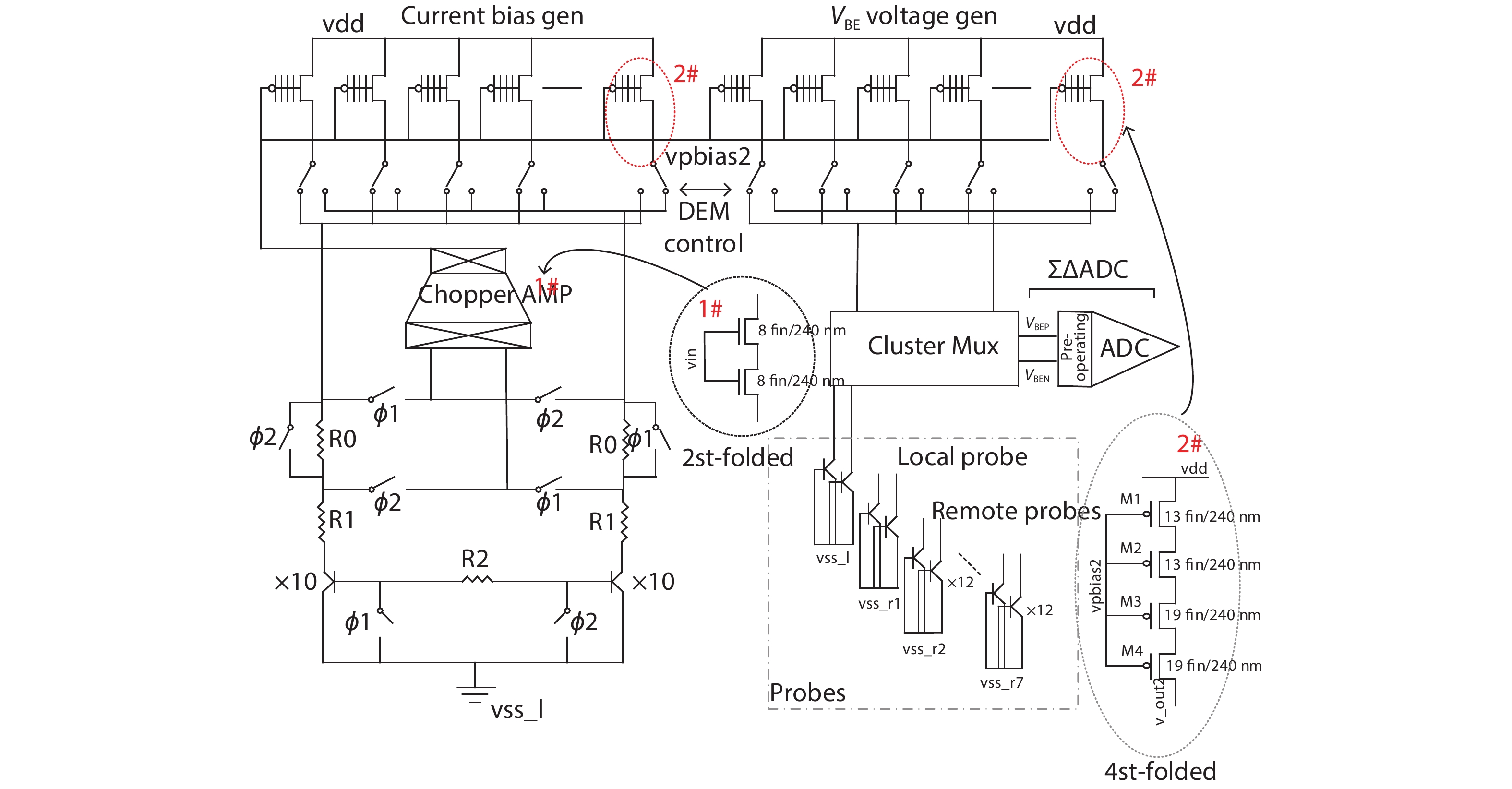
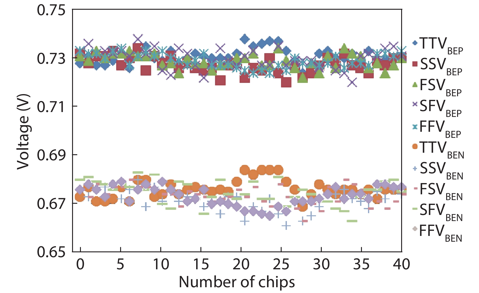
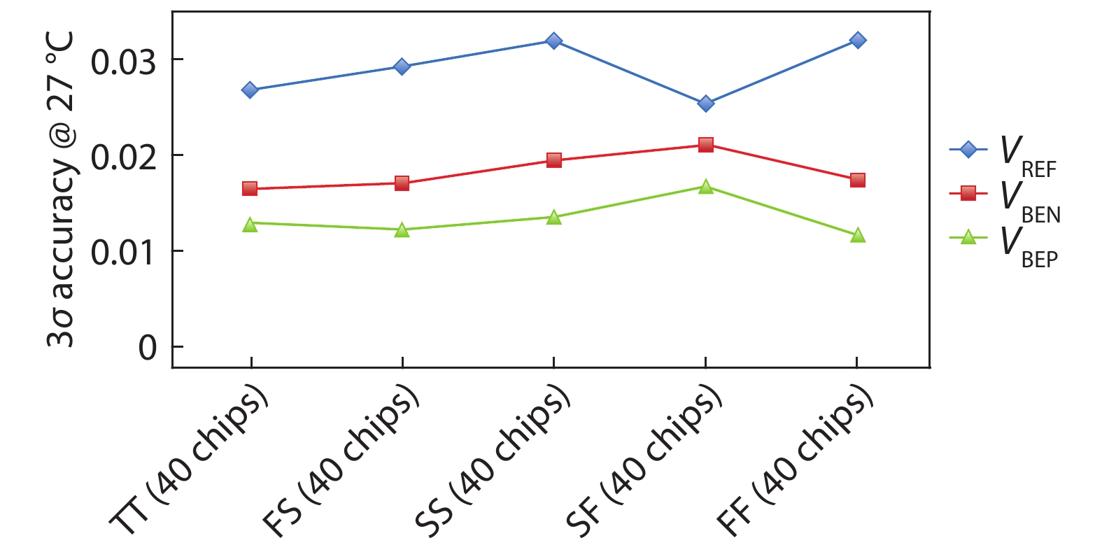
This paper presents a 1.2 V high accuracy thermal sensor analog front-end circuit with 7 probes placed around the microprocessor chip. This analog front-end consists of a BGR (bandgap reference), a DEM (dynamic element matching) control, and probes. The BGR generates the voltages linear changed with temperature, which are followed by the data read out circuits. The superior accuracy of the BGR’s output voltage is a key factor for sensors fabricated via the FinFET digital process. Here, a 4-stage folded current bias structure is proposed, to increase DC accuracy and confer immunity against FinFET process variation due to limited device length and low current bias. At the same time, DEM is also adopted, so as to filter out current branch mismatches. Having been fabricated via a 12 nm FinFET CMOS process, 200 chips were tested. The measurement results demonstrate that these analog front-end circuits can work steadily below 1.2 V, and a less than 3.1% 3σ-accuracy level is achieved. Temperature stability is 0.088 mV/°C across a range from –40 to 130 °C.


J. Semicond.
2021, 42(3): 032402 doi: 10.1088/1674-4926/42/3/032402
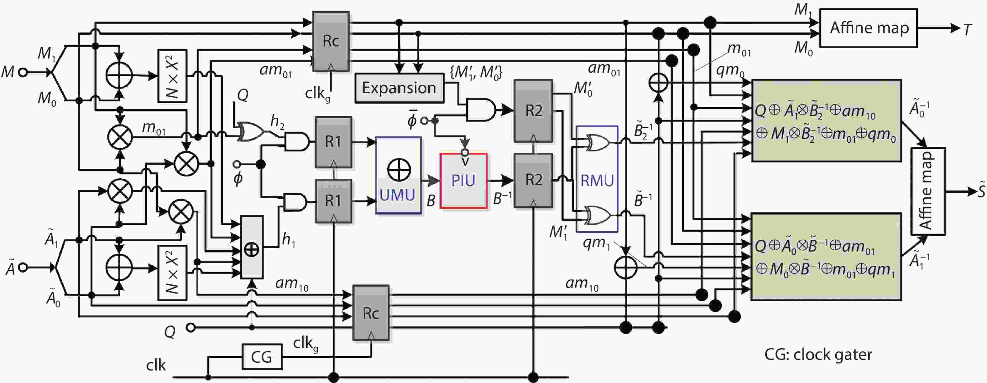
A side-channel attack (SCA)-resistant AES S-box implementation is proposed, which is an improvement from the power-aware hiding (PAH) S-box but with higher security and a smaller area. We use the composite field approach and apply the PAH method to the inversion in the nonlinear kernel and a masking method to the other parts. In addition, a delay-matched enable control technique is used to suppress glitches in the masked parts. The evaluation results show that its area is contracted to 63.3% of the full PAH S-box, and its power-delay product is much lower than that of the masking implementation. The leakage assessment using simulation power traces concludes that it has no detectable leakage under t-test and that it at least can thwart the moment-correlation analysis using 665 000 noiseless traces.


J. Semicond.
2021, 42(3): 032501 doi: 10.1088/1674-4926/42/3/032501
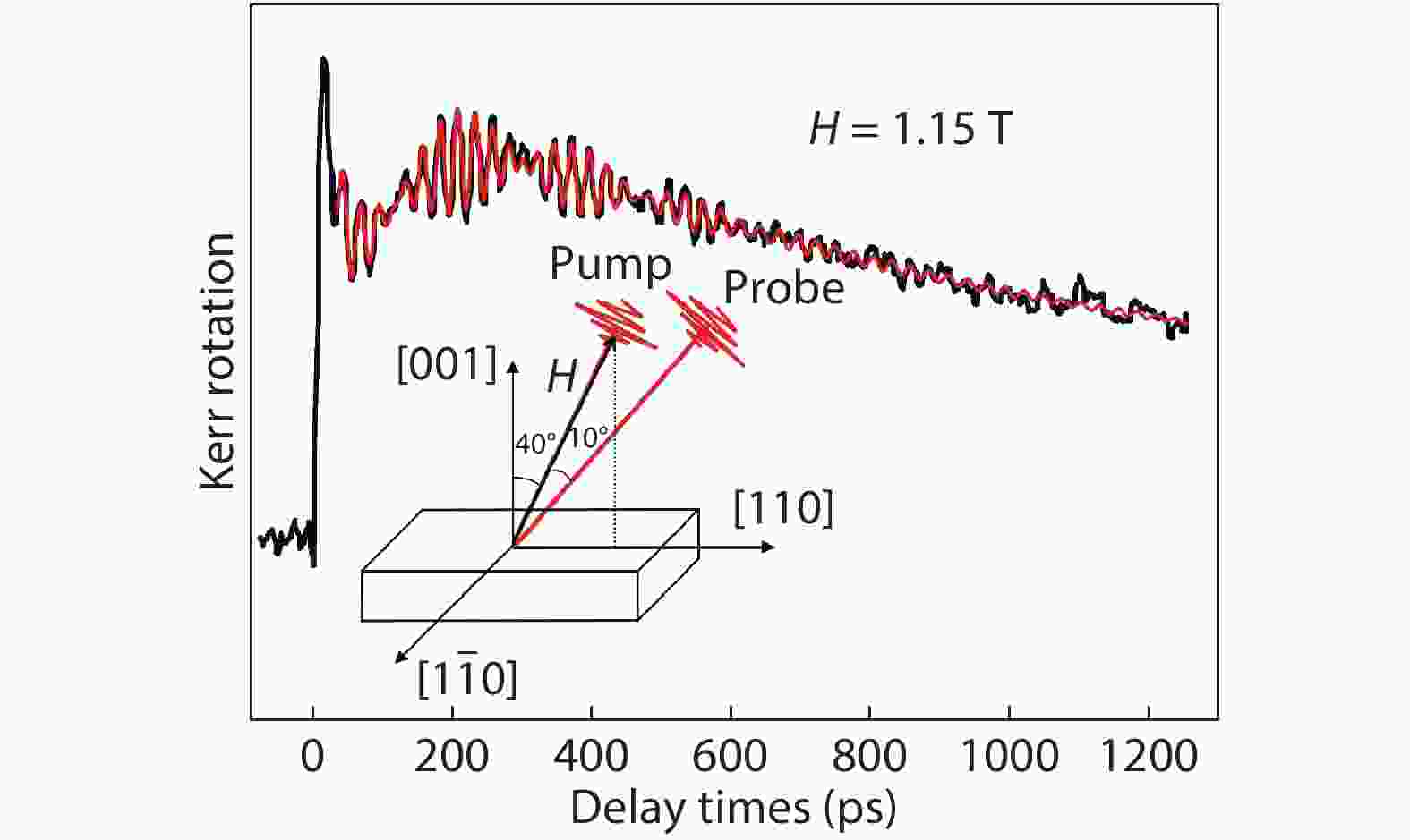
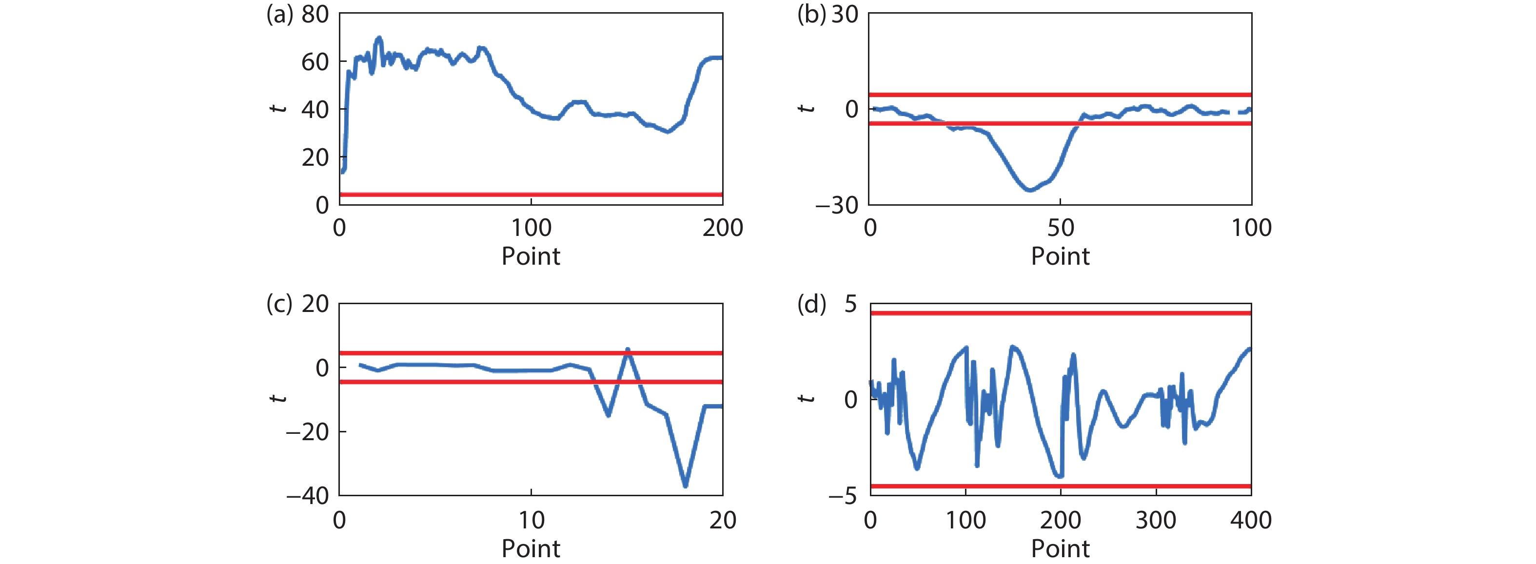
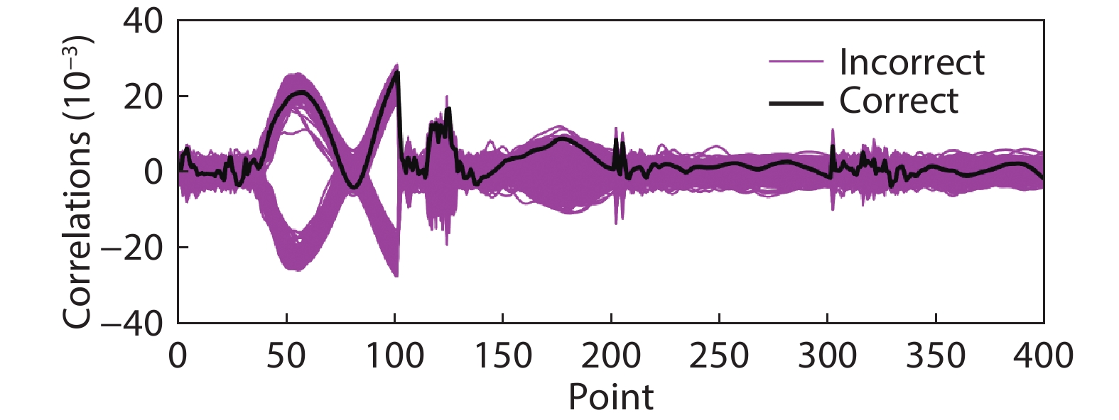
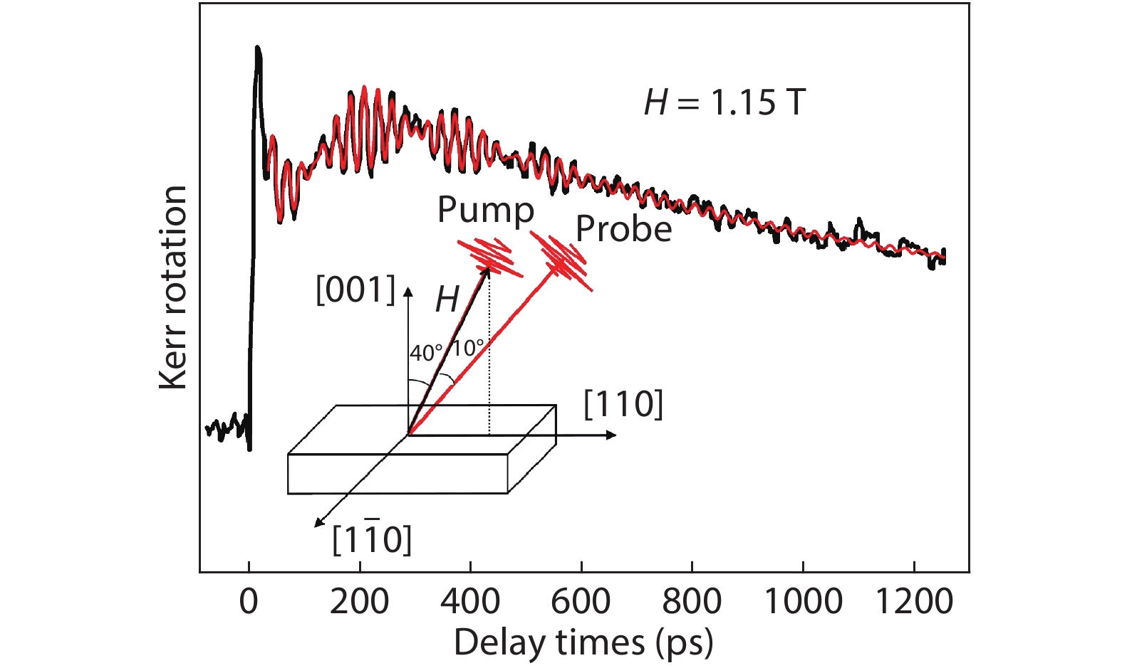
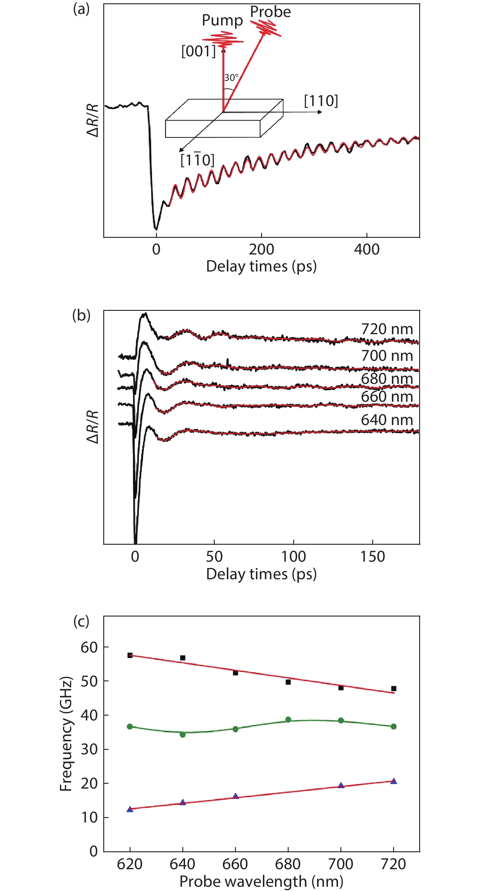
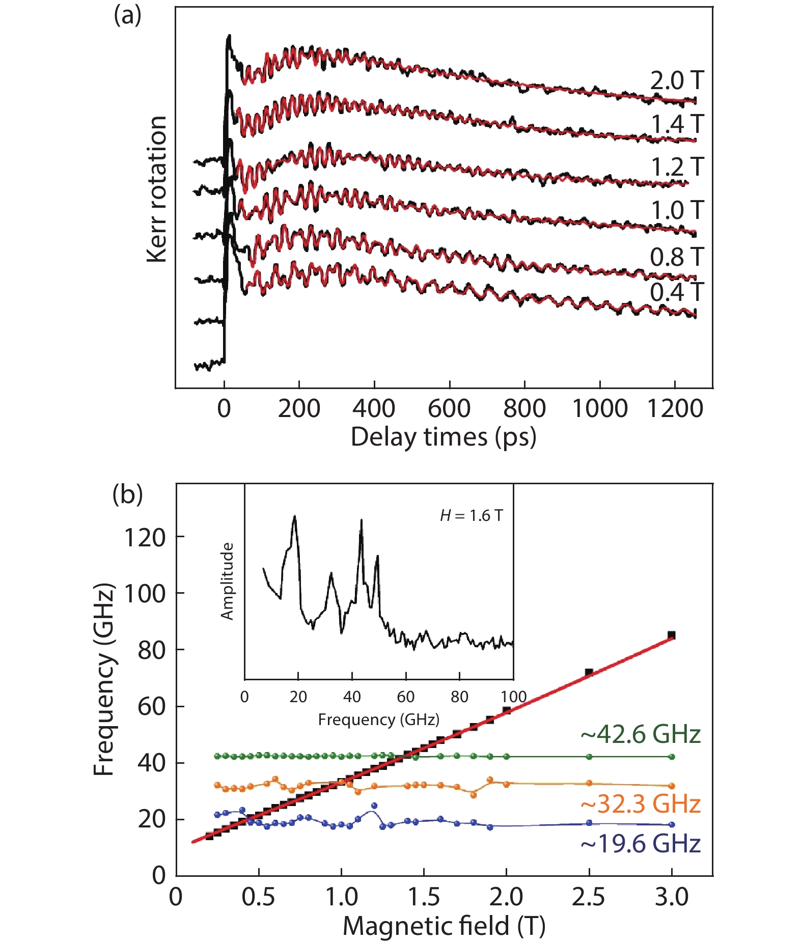
The magnetic dynamics of a thin Co2FeAl film epitaxially grown on GaAs substrate was investigated using the time-resolved magneto-optical Kerr measurement under an out-of-plane external field. The intrinsic magnetic damping constant, which should do not vary with the external magnetic field, exhibits an abnormal huge increase when the precession frequency is tuned to be resonant with that of the coherent longitudinal acoustic phonon in the Co2FeAl/GaAs heterostructure. The experimental finding is suggested to result from the strong coherent energy transfer from spins to acoustic phonons via magnetoelastic effect under a resonant coupling condition, which leads to a huge energy dissipation of spins and a greatly enhanced magnetic damping in Co2FeAl. Our experimental findings provide an experimental evidence of spin pumping-like effect driven by propagating acoustic phonons via magnetoelastic effect, suggesting an alternative approach to the possible long-range spin manipulation via coherent acoustic waves.

J. Semicond.
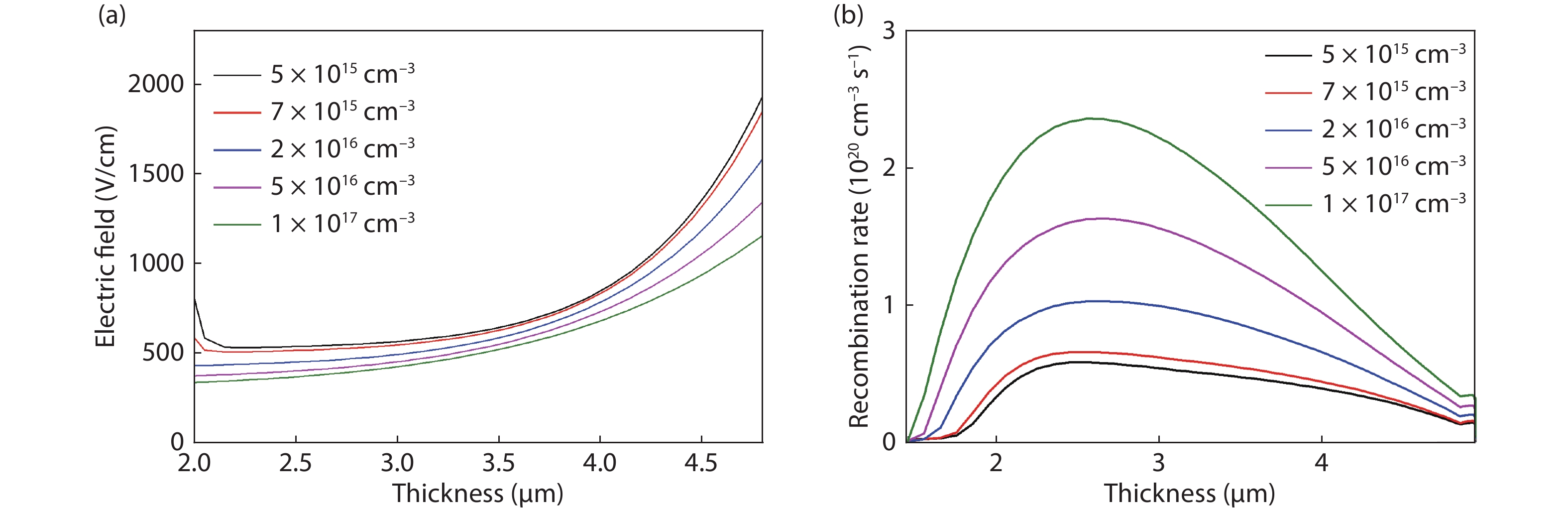
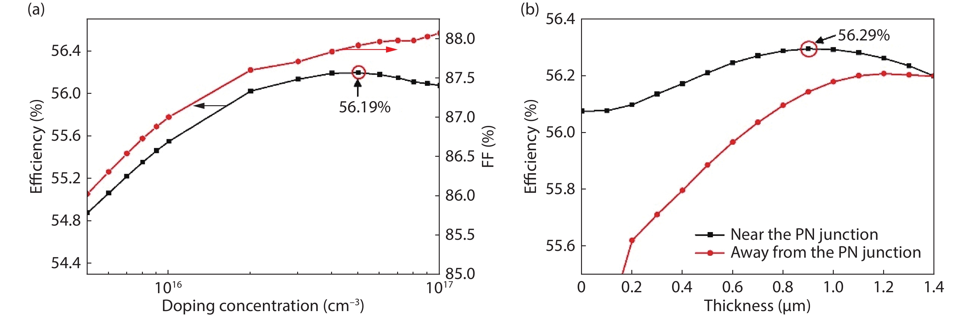
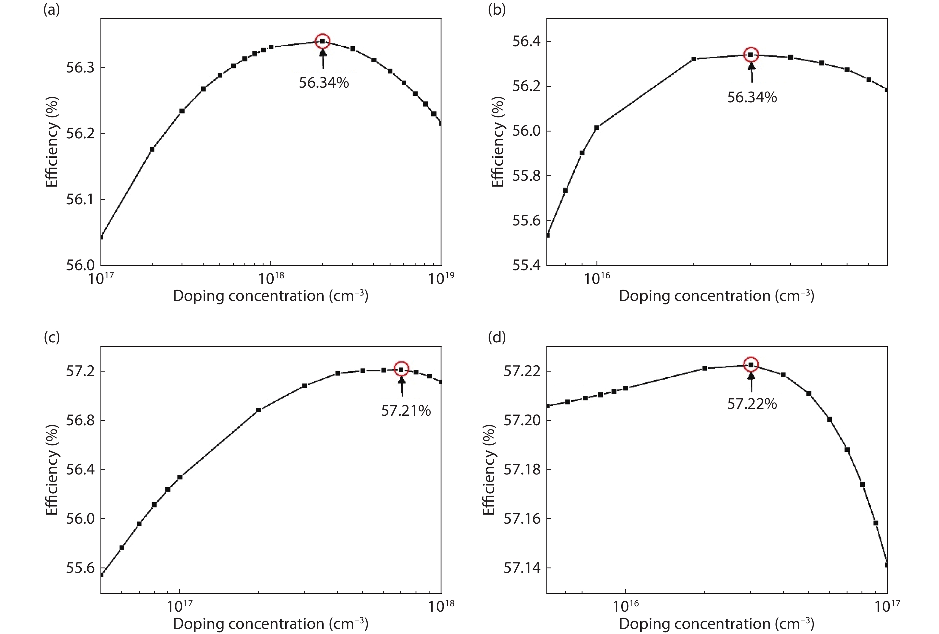
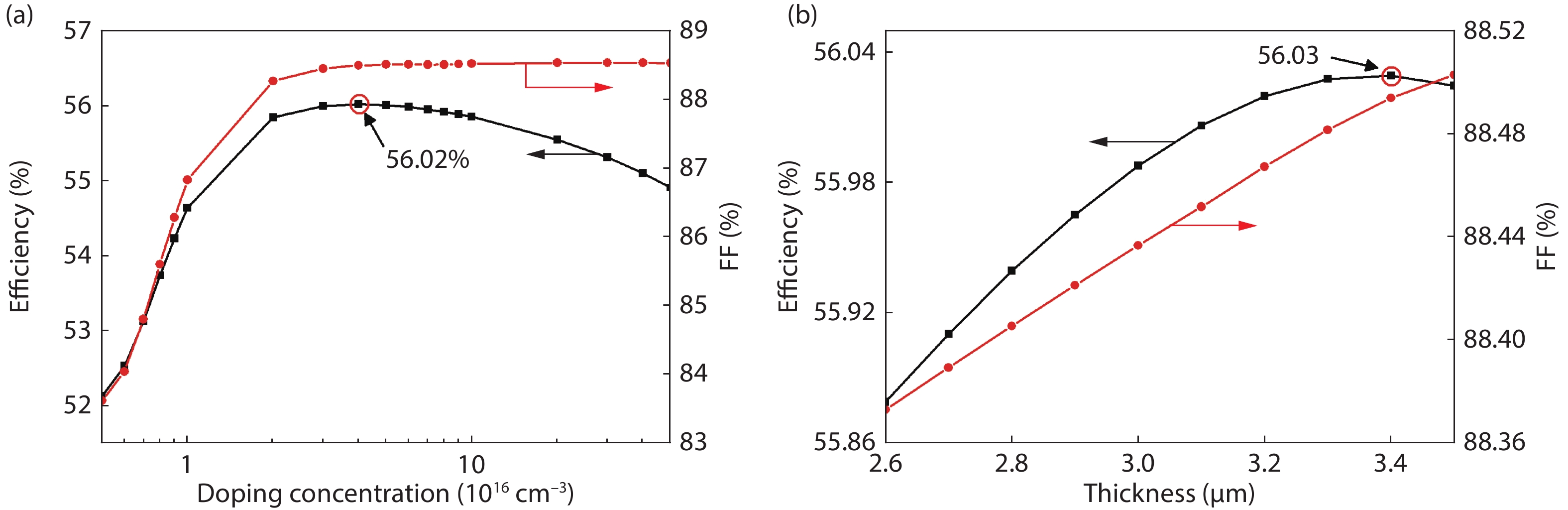
2021, 42(3): 032701 doi: 10.1088/1674-4926/42/3/032701
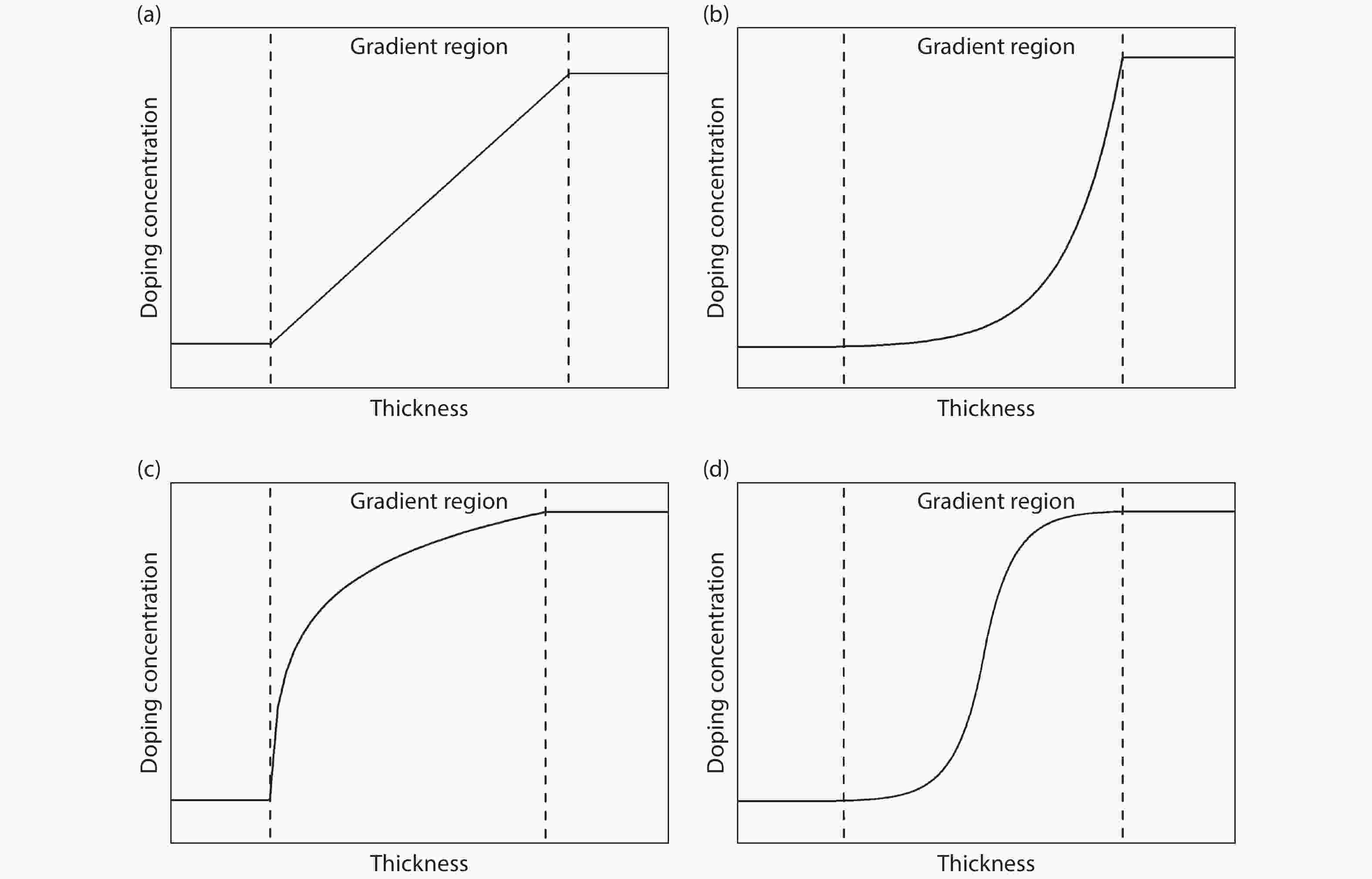
The gradient doping regions were employed in the emitter layer and the base layer of GaAs based laser power converters (LPCs). Silvaco TCAD was used to numerically simulate the linear gradient doping and exponential gradient doping structure, and analyze the transport process of photogenerated carriers. Energy band adjustment via gradient doping improved the separation and transport efficiency of photogenerated carriers and reduced the total recombination rate of GaAs LPCs. Compared with traditional structure of LPCs, the photoelectric conversion efficiency of LPCs with linear and exponential gradient doping structure were improved from 52.7% to 57.2% and 57.7%, respectively, under 808 nm laser light at the power density of 1 W/cm2.