Issue Browser
Volume 43, Issue 2,
Feb 2022
Column


J. Semicond.
2022, 43(2): 021301 doi: 10.1088/1674-4926/43/2/021301
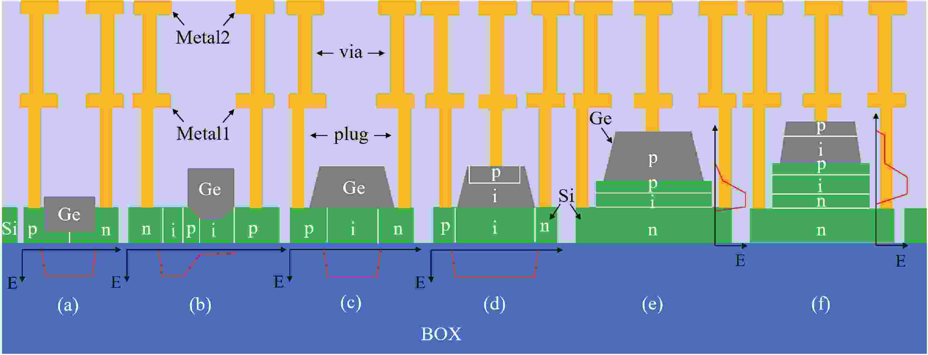
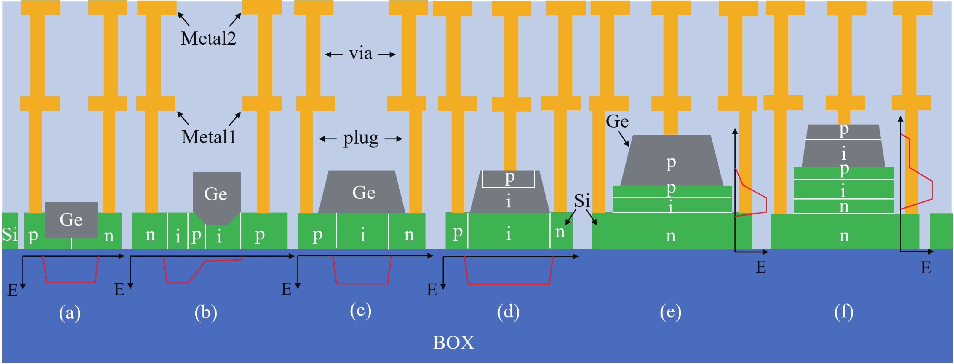
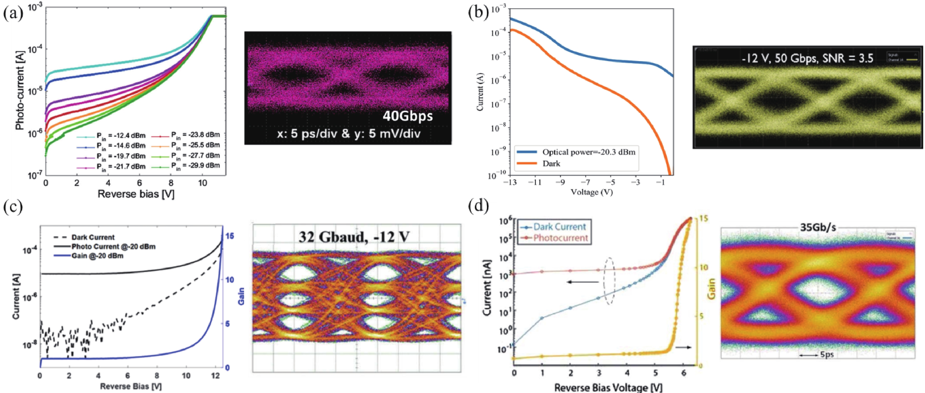
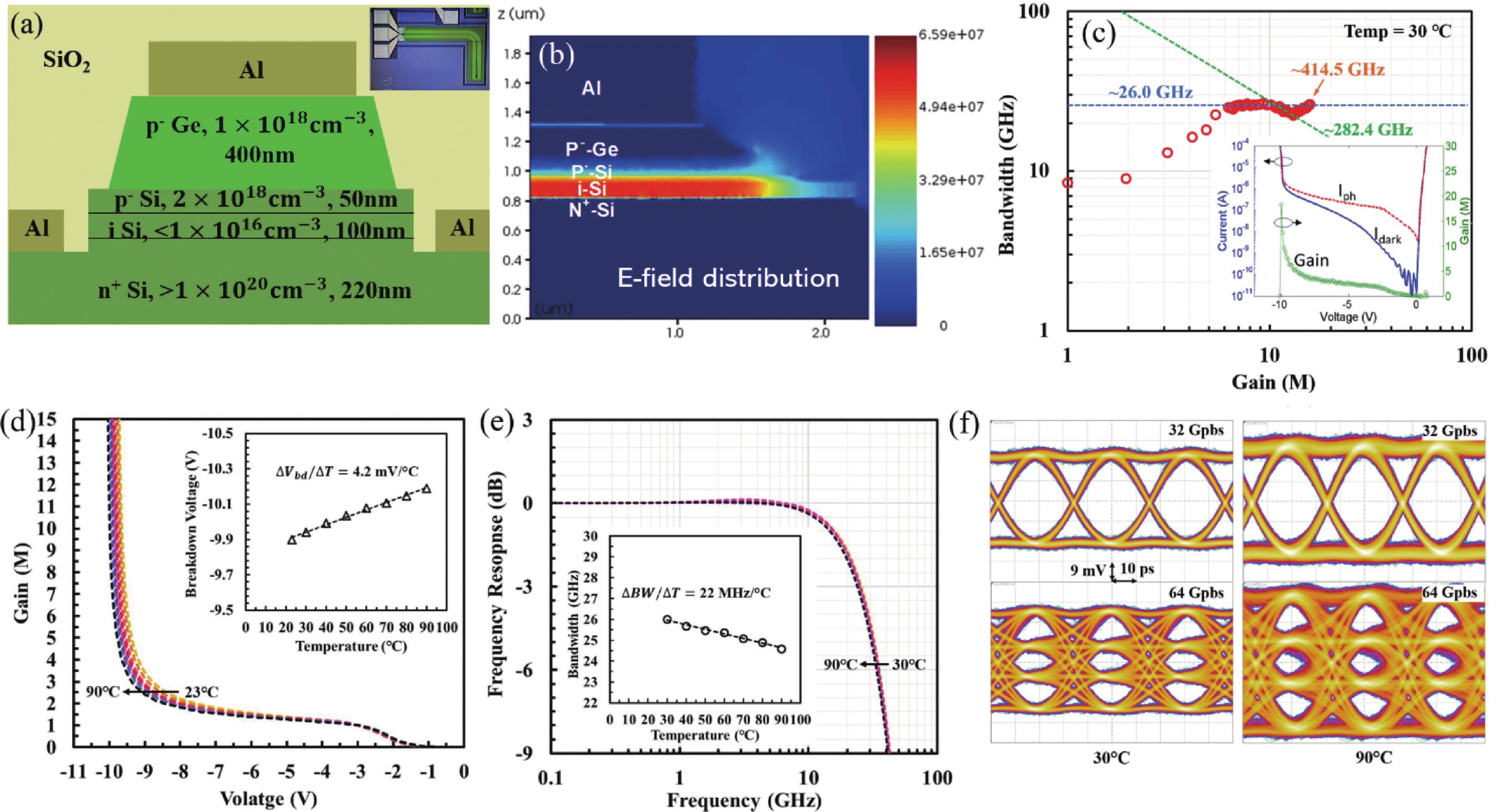
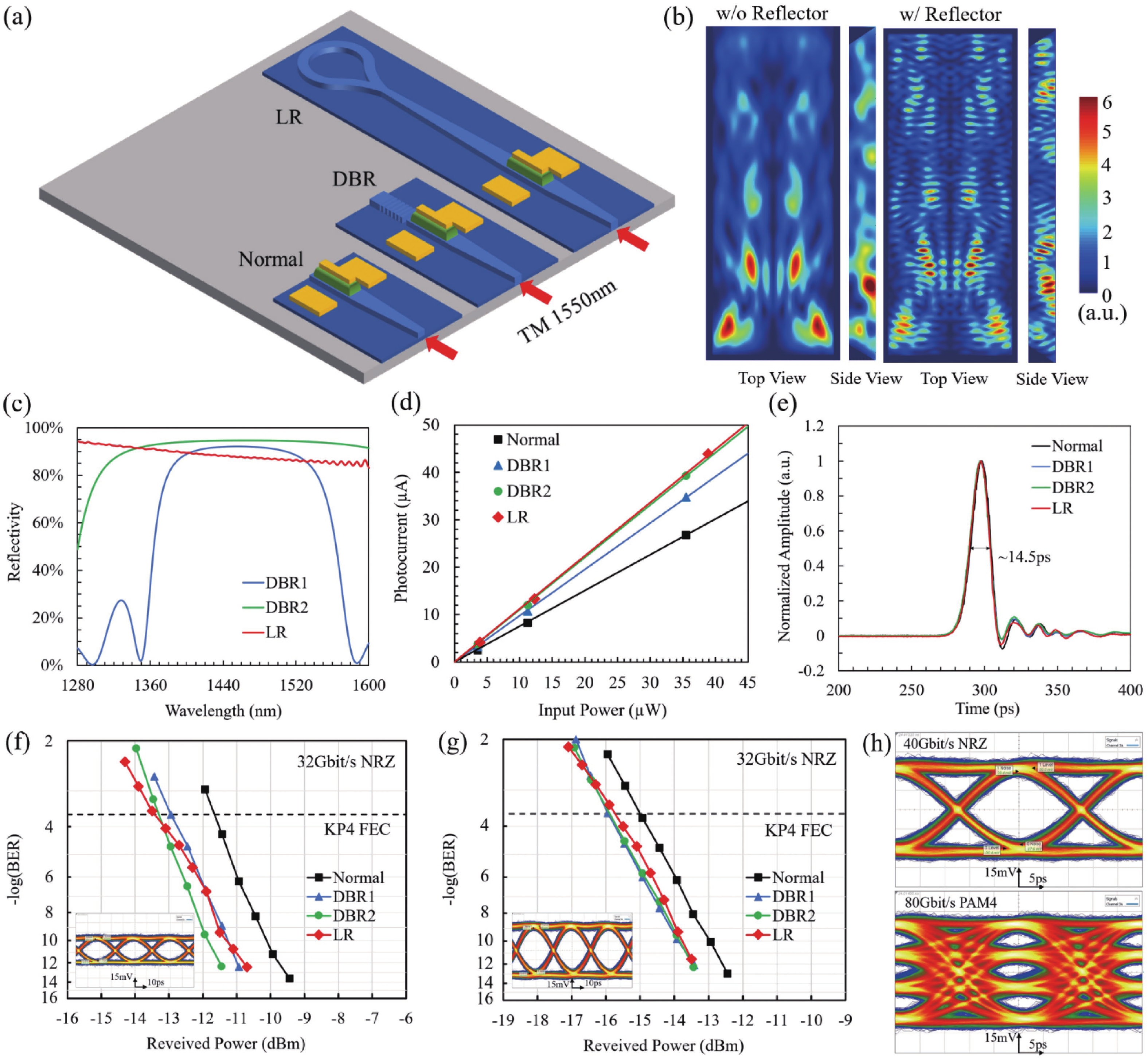
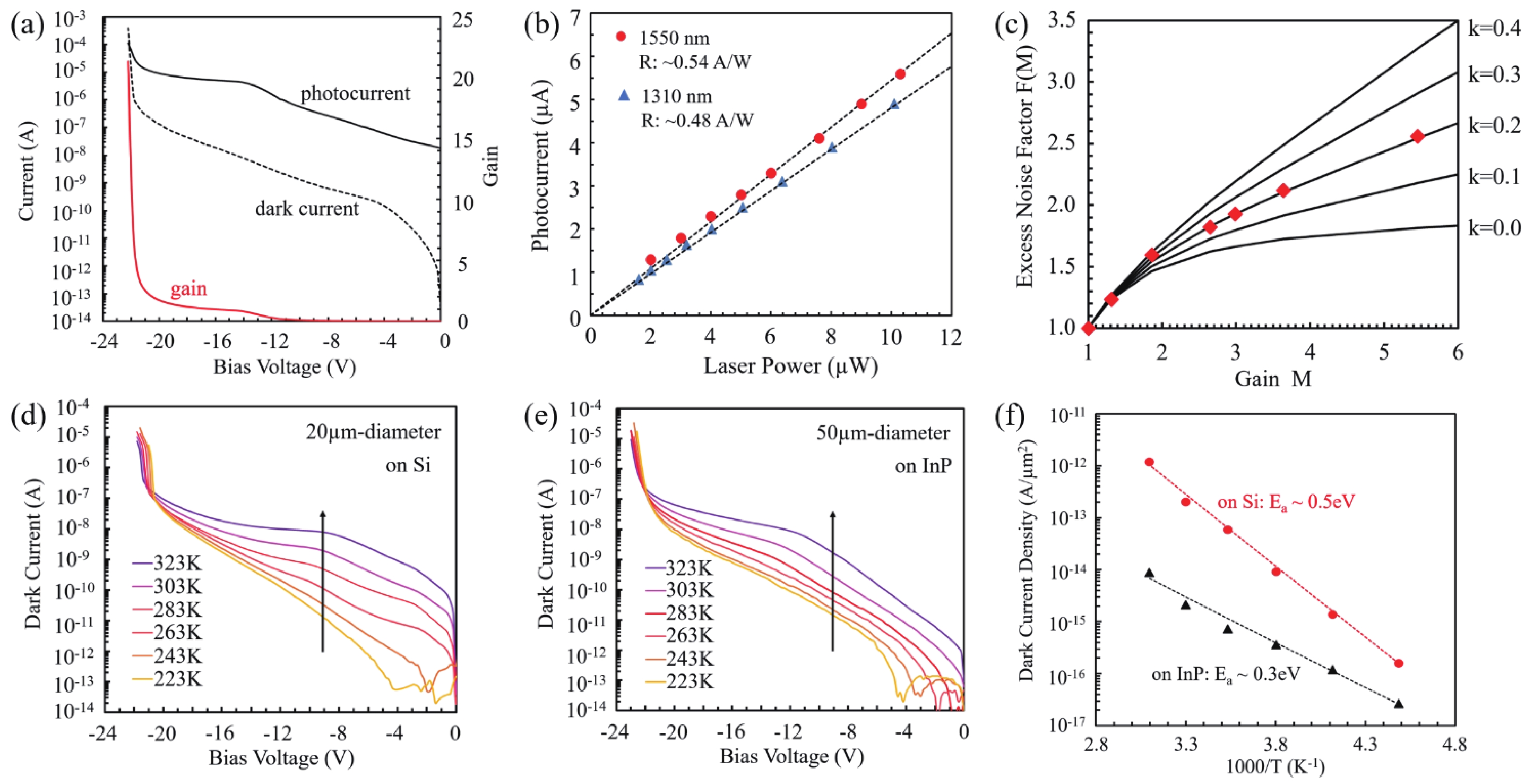
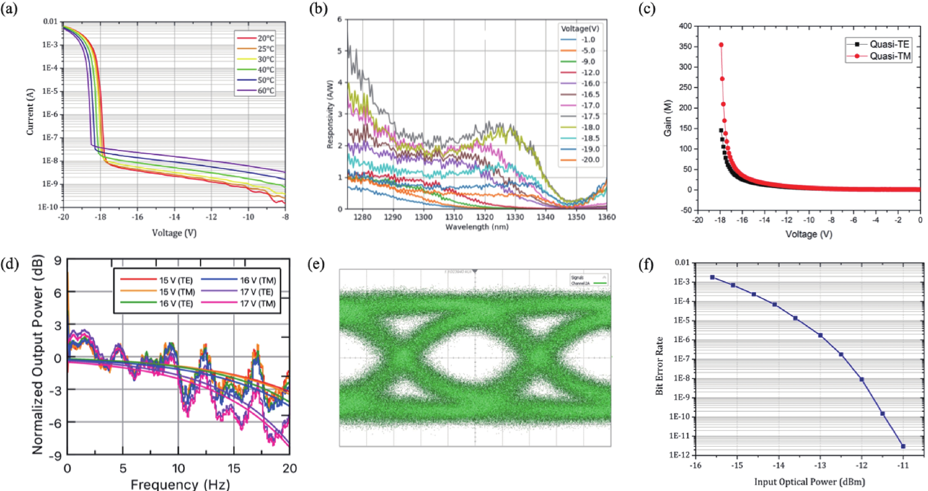
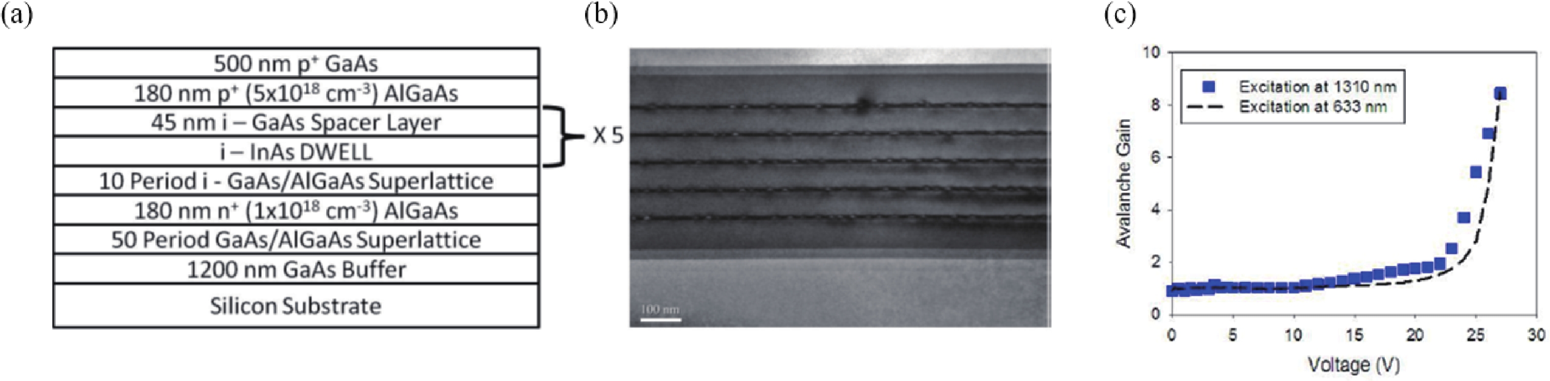
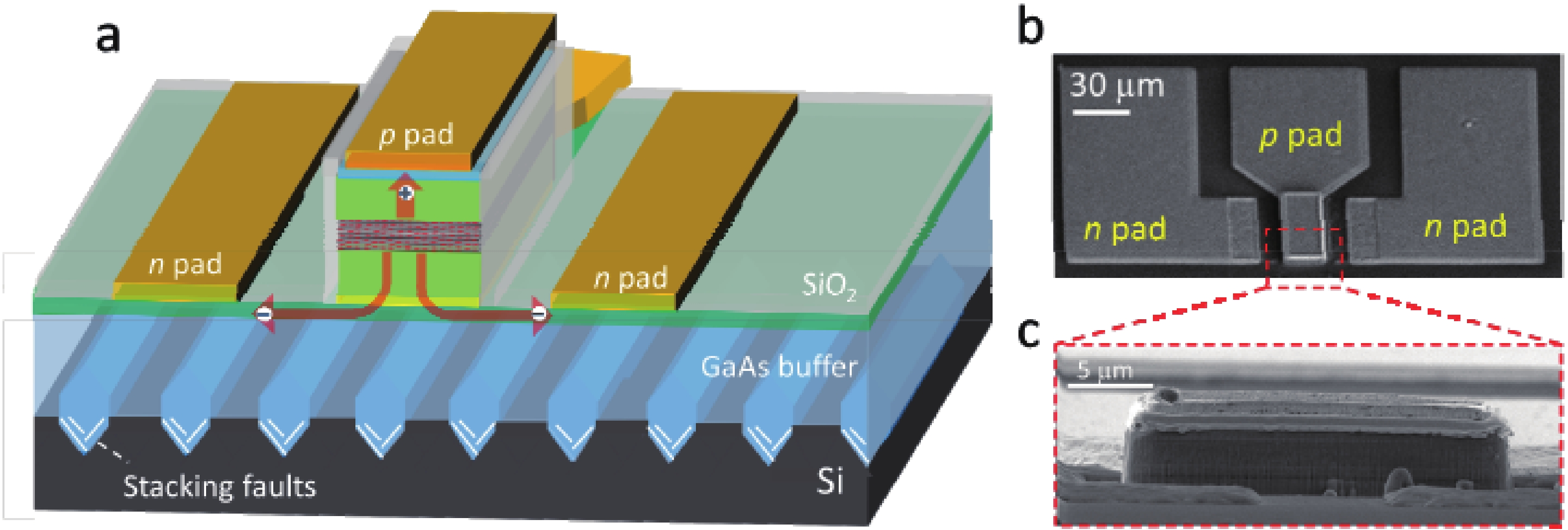
Silicon photonics technology has drawn significant interest due to its potential for compact and high-performance photonic integrated circuits. The Ge- or III–V material-based avalanche photodiodes integrated on silicon photonics provide ideal high sensitivity optical receivers for telecommunication wavelengths. Herein, the last advances of monolithic and heterogeneous avalanche photodiodes on silicon are reviewed, including different device structures and semiconductor systems.


J. Semicond.
2022, 43(2): 021701 doi: 10.1088/1674-4926/43/2/021701
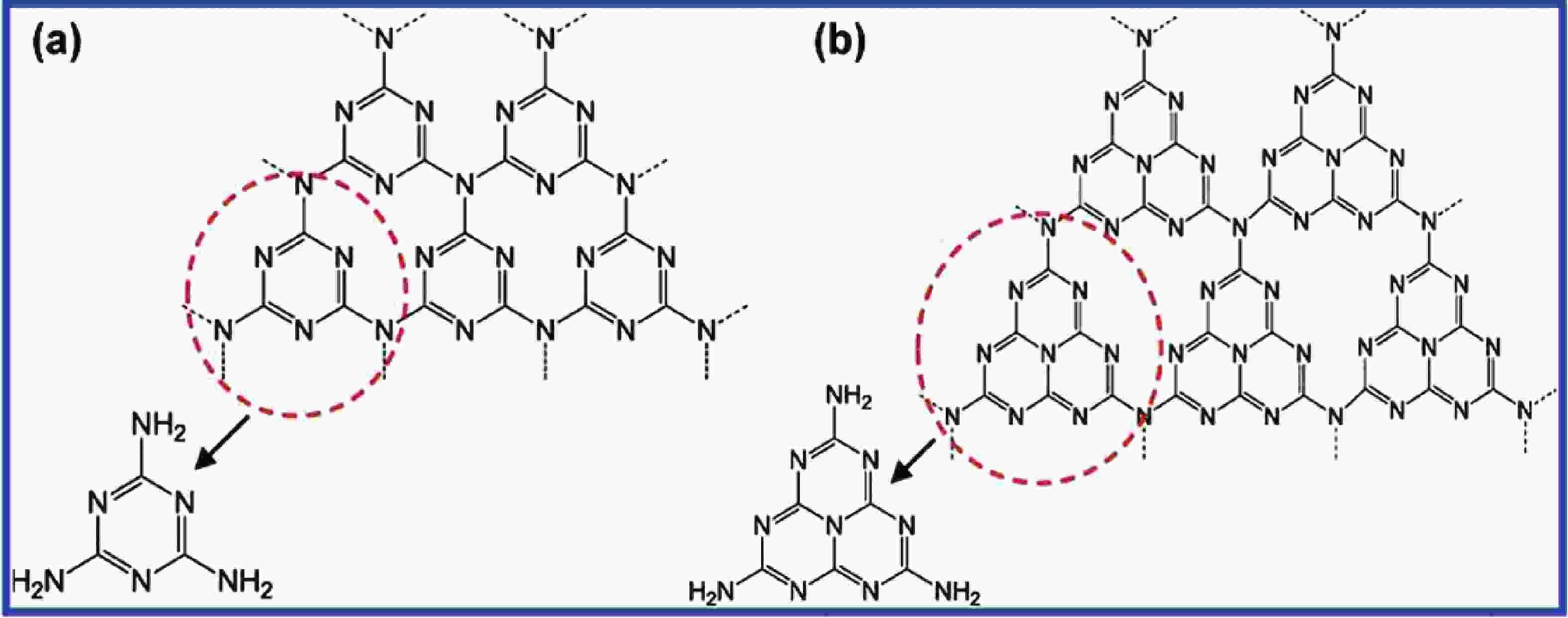
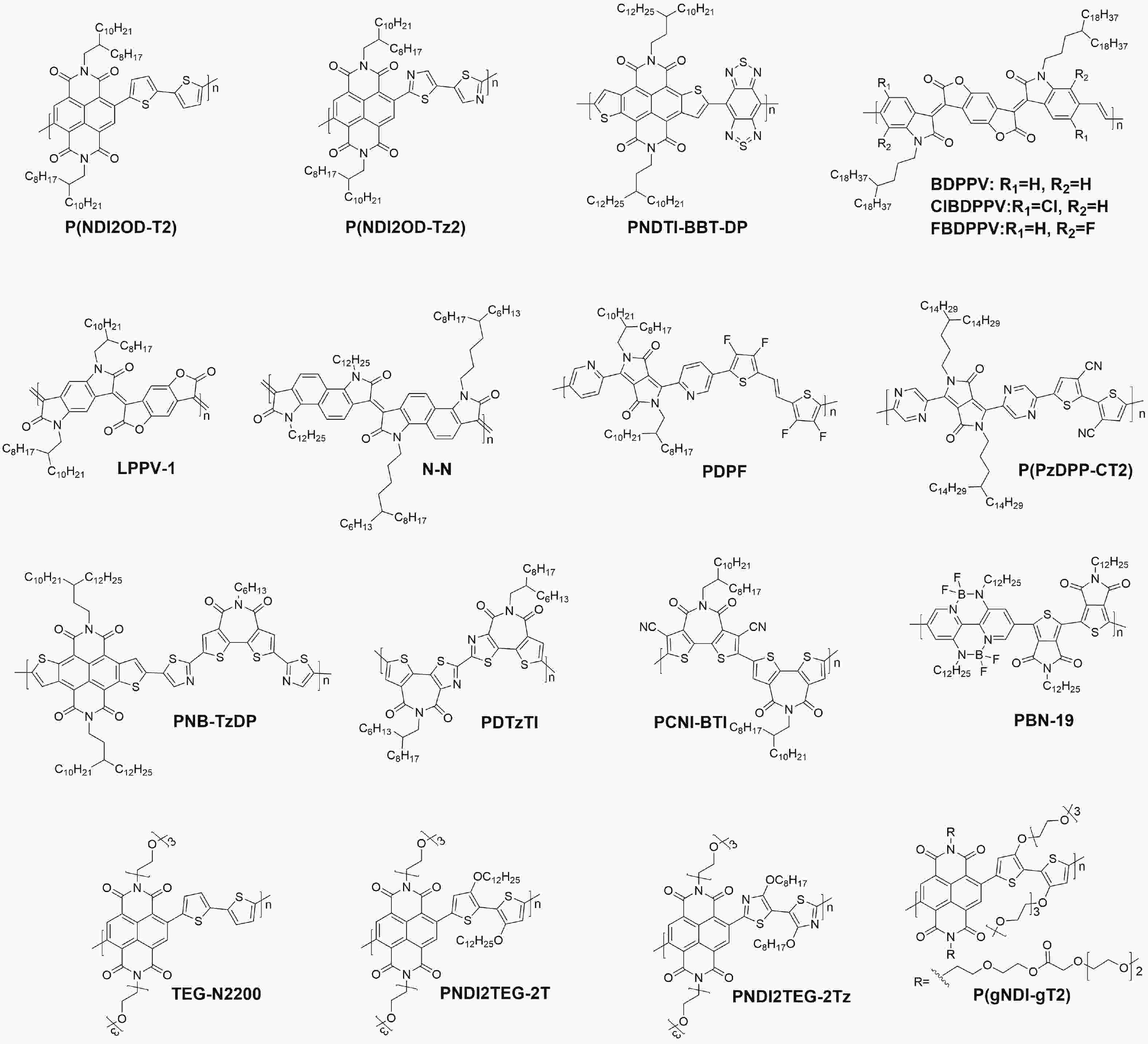
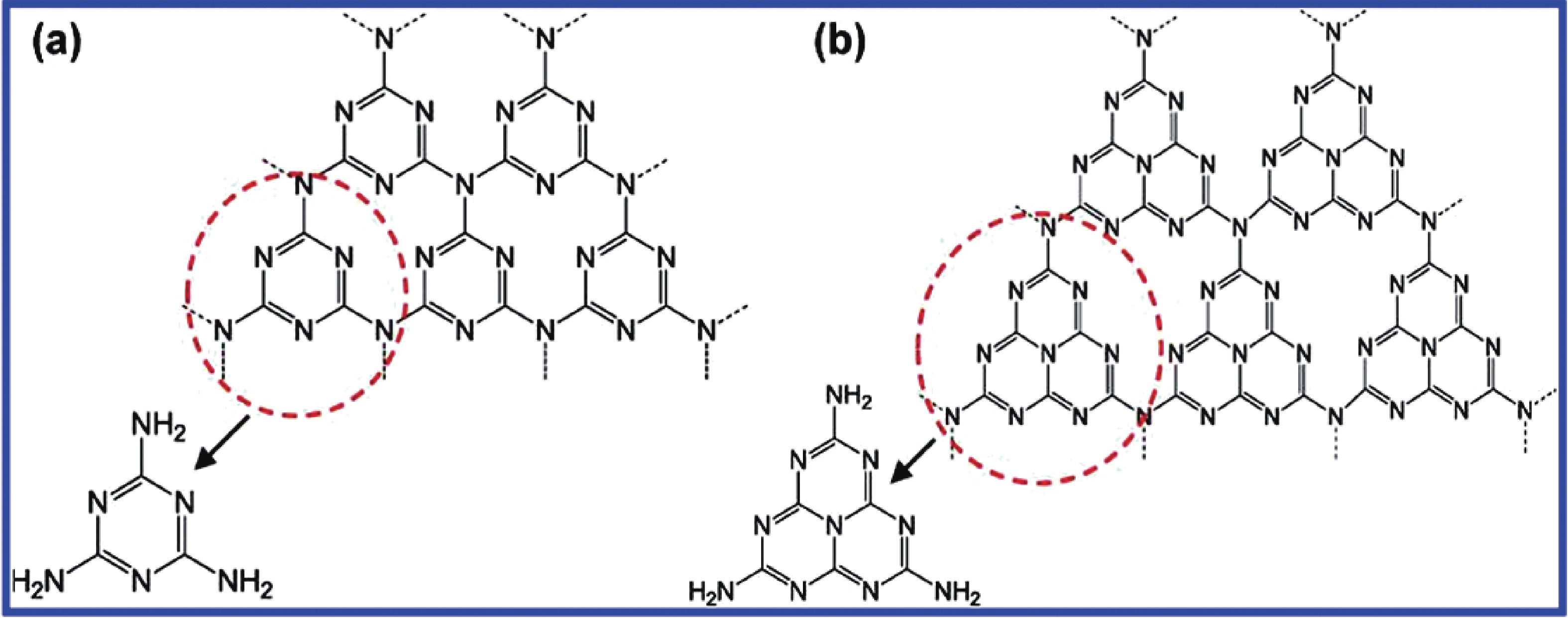
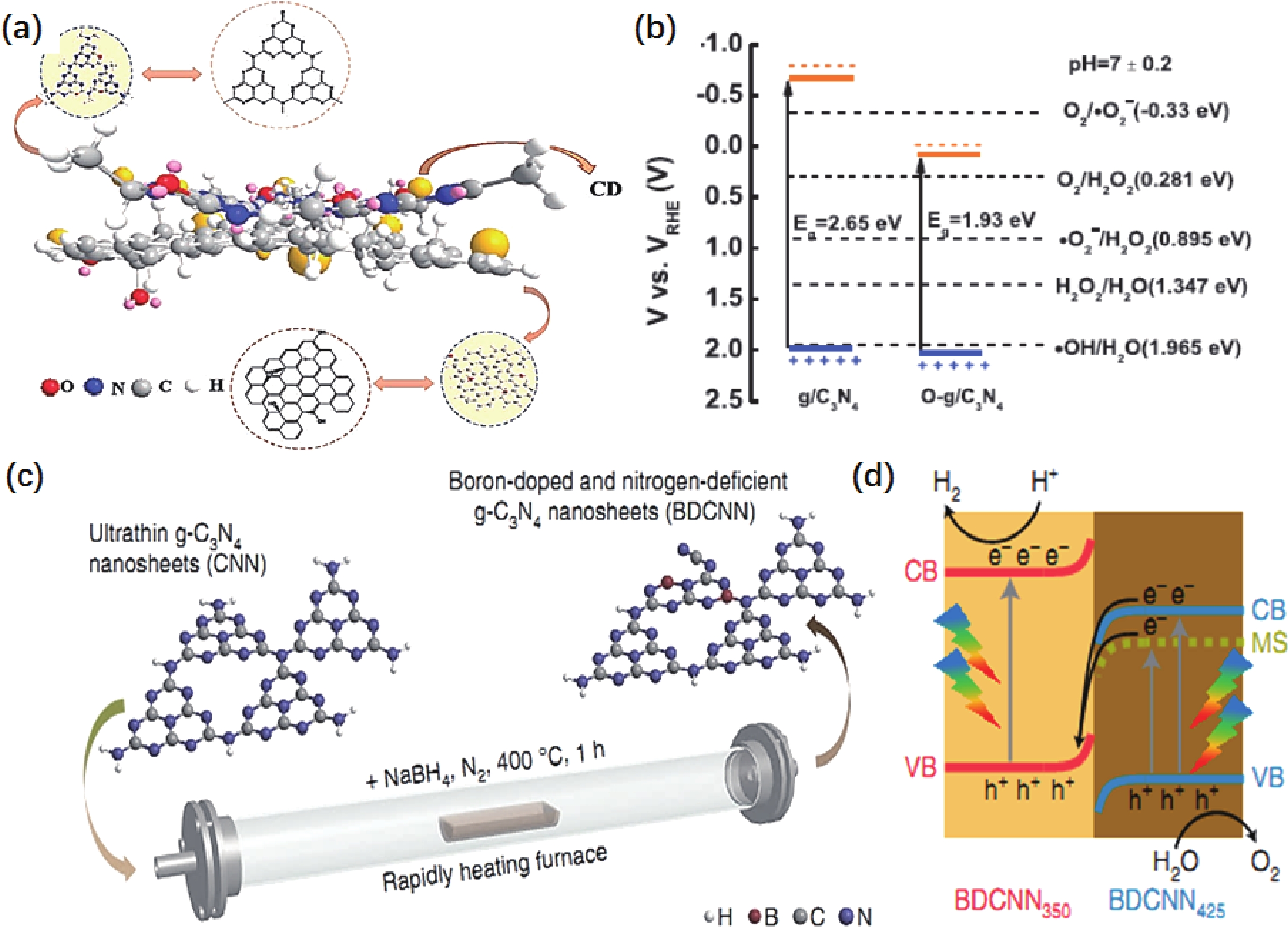
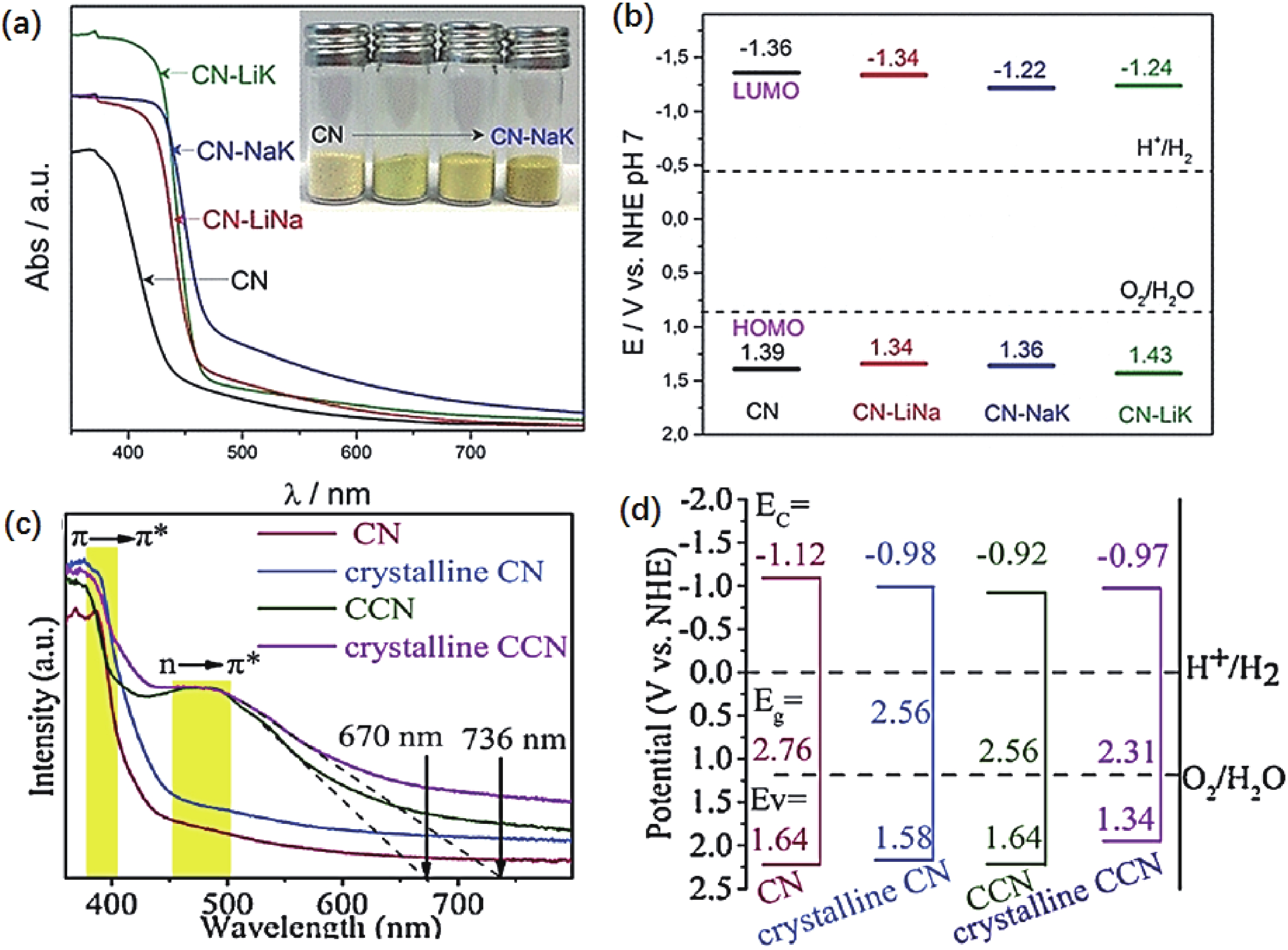
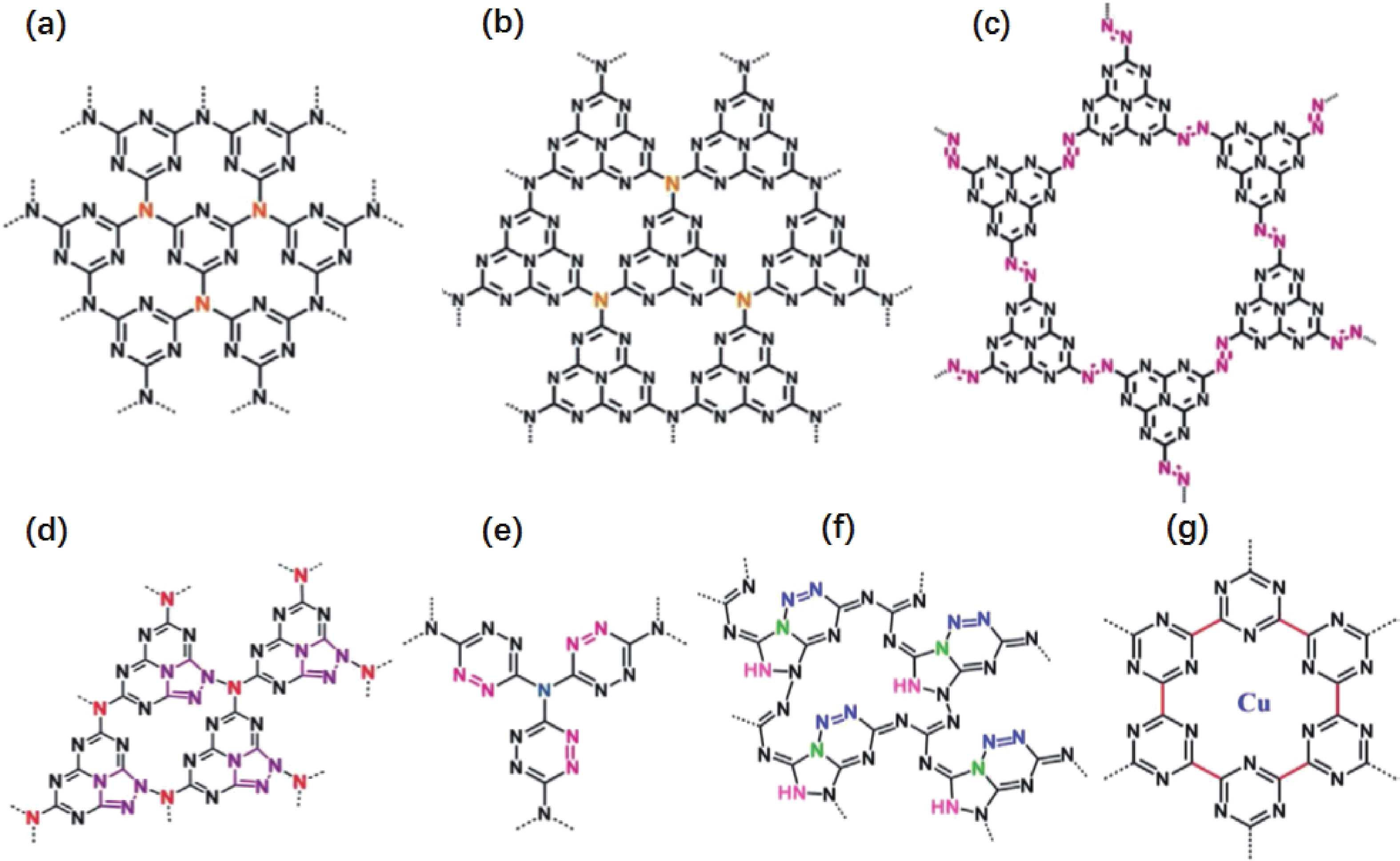
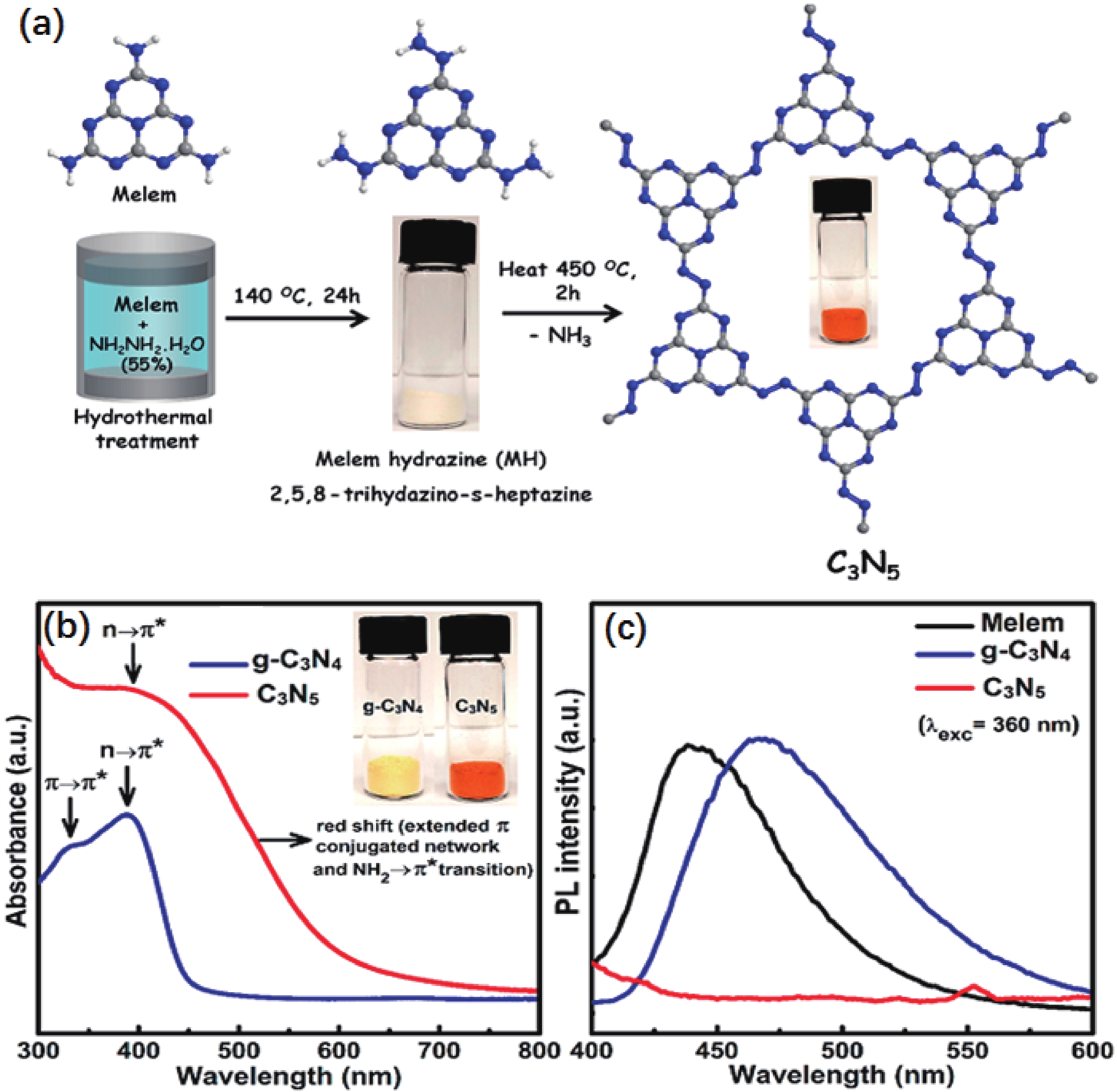
The utilization of solar energy to drive energy conversion and simultaneously realize pollutant degradation via photocatalysis is one of most promising strategies to resolve the global energy and environment issues. During the past decade, graphite carbon nitride (g-C3N4) has attracted dramatically growing attention for solar energy conversion due to its excellent physicochemical properties as a photocatalyst. However, its practical application is still impeded by several limitations and shortcomings, such as high recombination rate of charge carriers, low visible-light absorption, etc. As an effective solution, the electronic structure tuning of g-C3N4 has been widely adopted. In this context, firstly, the paper critically focuses on the different strategies of electronic structure tuning of g-C3N4 like vacancy modification, doping, crystallinity modulation and synthesis of a new molecular structure. And the recent progress is reviewed. Finally, the challenges and future trends are summarized.


J. Semicond.
2022, 43(2): 021801 doi: 10.1088/1674-4926/43/2/021801
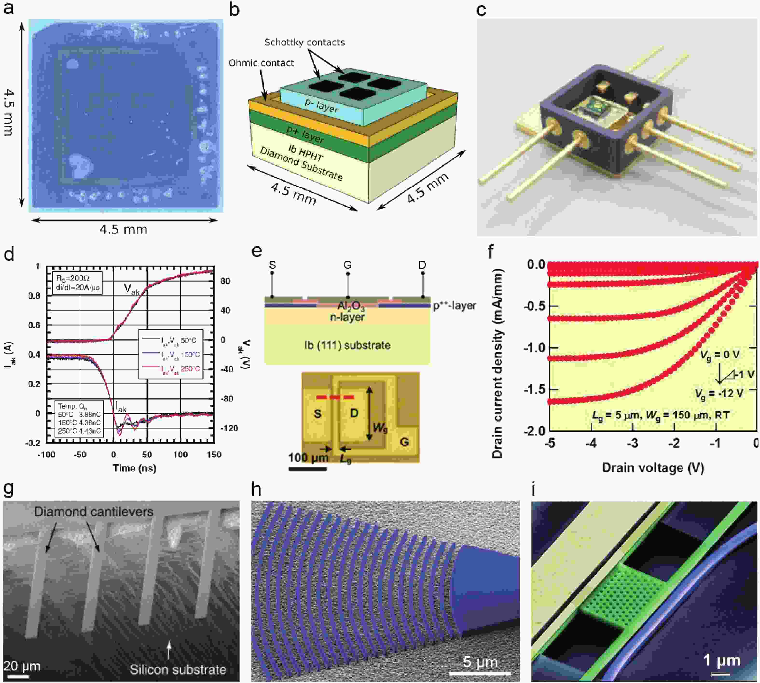
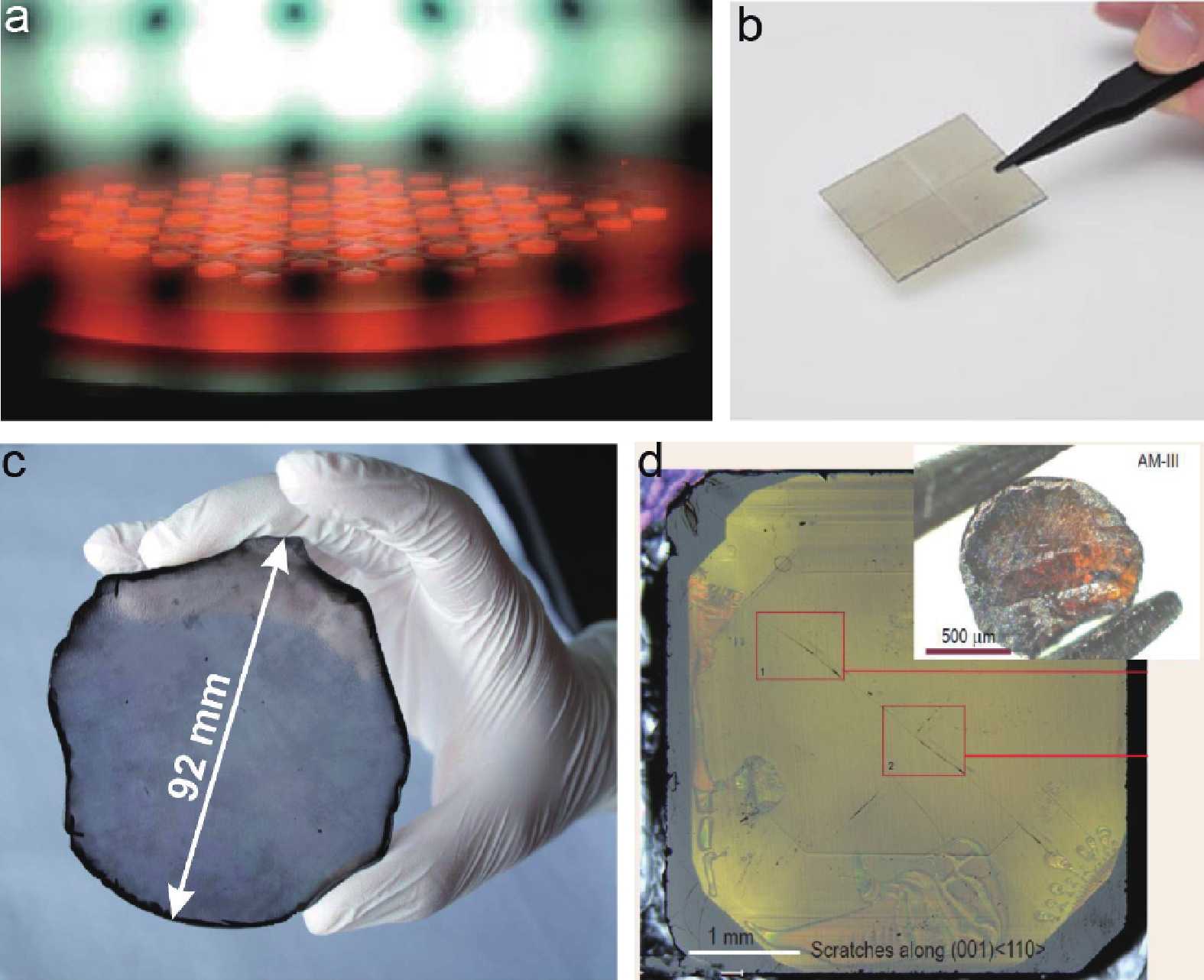
Diamond, as an ultra-wide bandgap semiconductor, has become a promising candidate for next-generation microelectronics and optoelectronics due to its numerous advantages over conventional semiconductors, including ultrahigh carrier mobility and thermal conductivity, low thermal expansion coefficient, and ultra-high breakdown voltage, etc. Despite these extraordinary properties, diamond also faces various challenges before being practically used in the semiconductor industry. This review begins with a brief summary of previous efforts to model and construct diamond-based high-voltage switching diodes, high-power/high-frequency field-effect transistors, MEMS/NEMS, and devices operating at high temperatures. Following that, we will discuss recent developments to address scalable diamond device applications, emphasizing the synthesis of large-area, high-quality CVD diamond films and difficulties in diamond doping. Lastly, we show potential solutions to modulate diamond’s electronic properties by the “elastic strain engineering” strategy, which sheds light on the future development of diamond-based electronics, photonics and quantum systems.


J. Semicond.
2022, 43(2): 023101 doi: 10.1088/1674-4926/43/2/023101

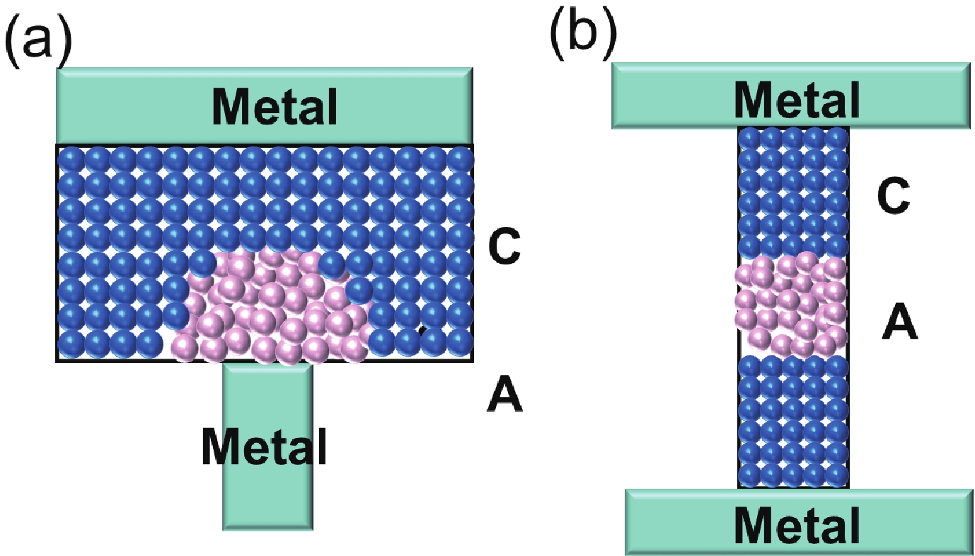
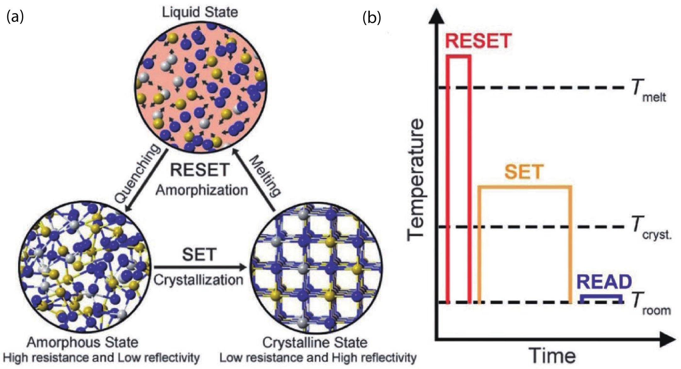
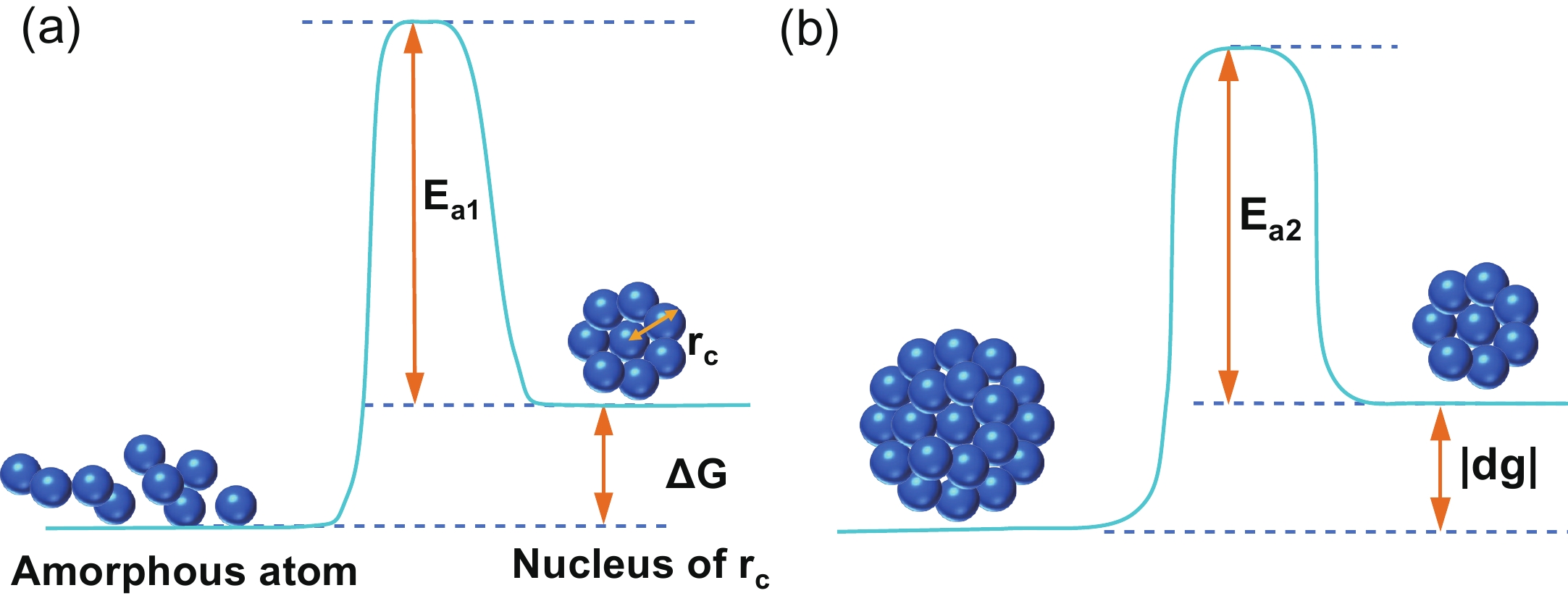
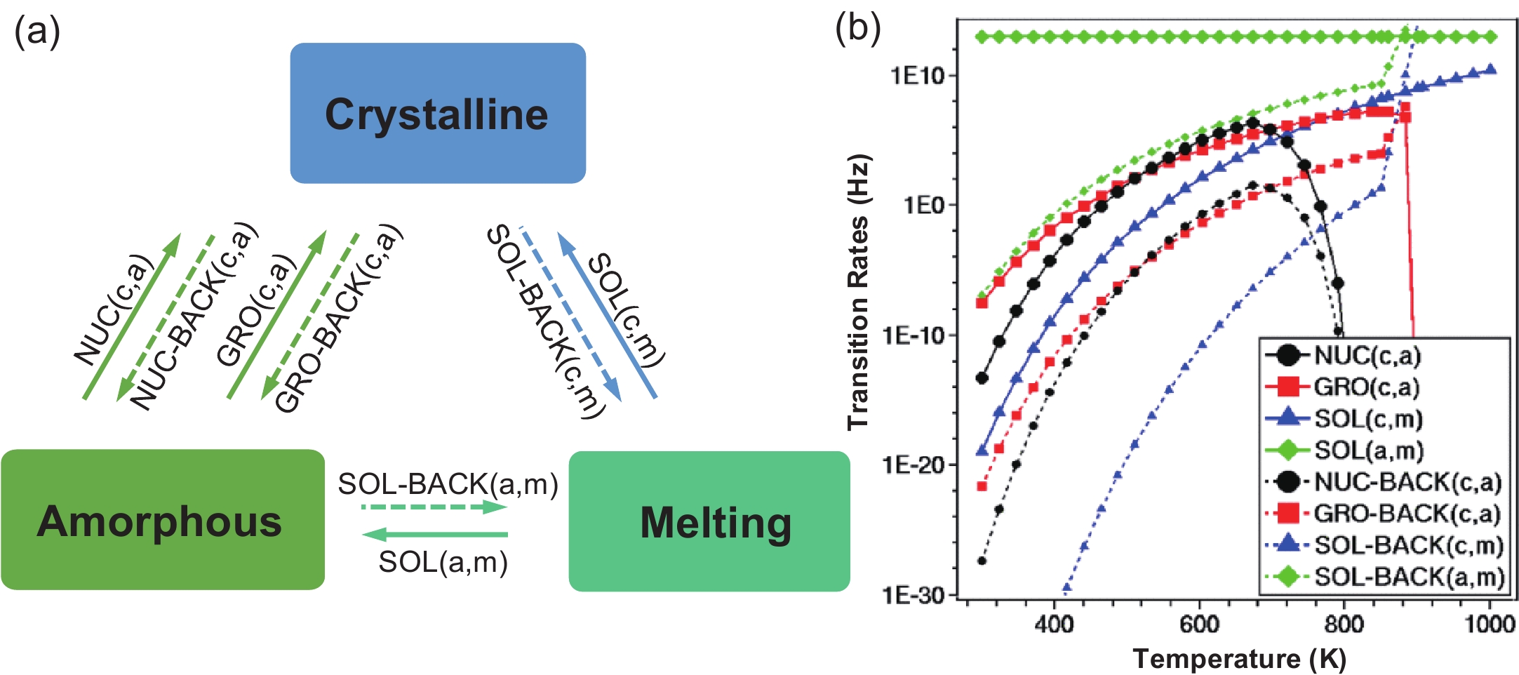
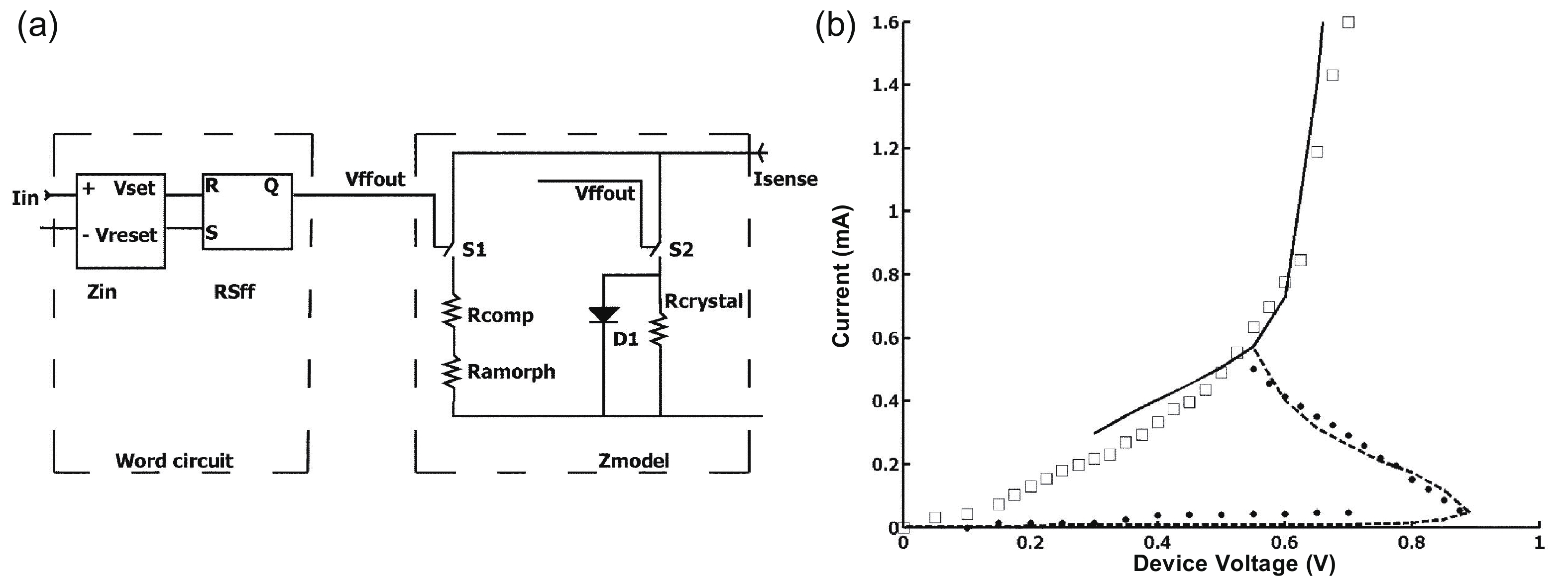
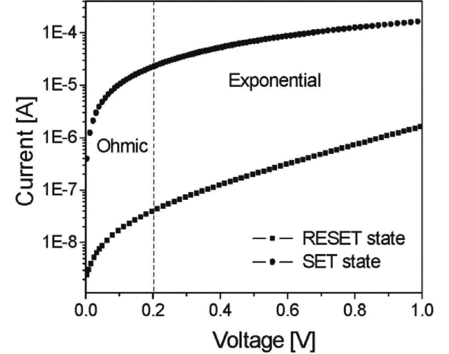
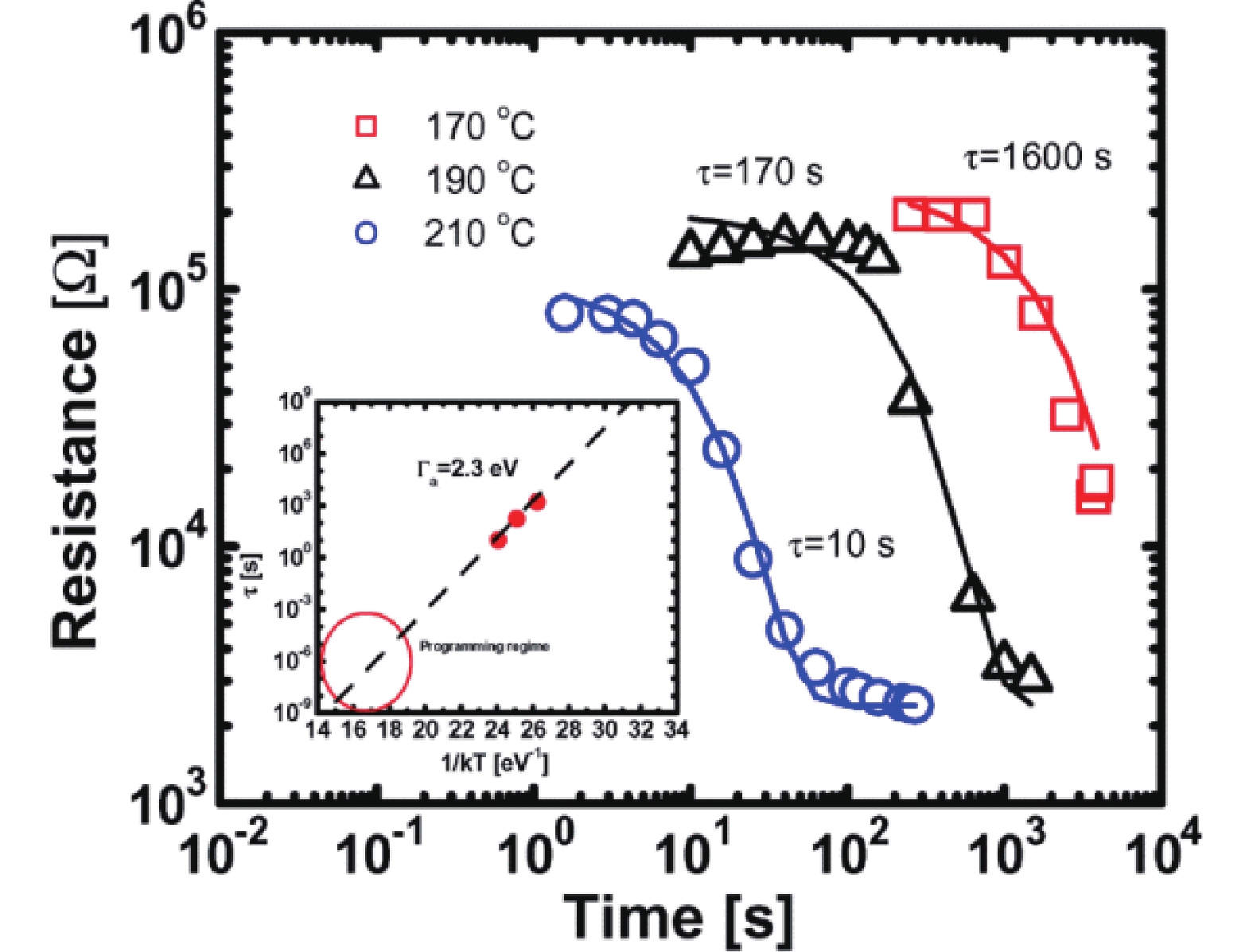
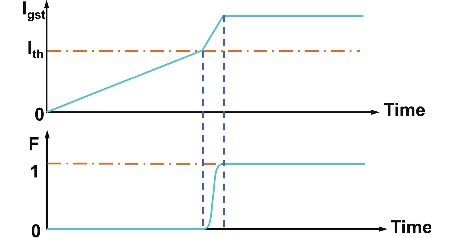
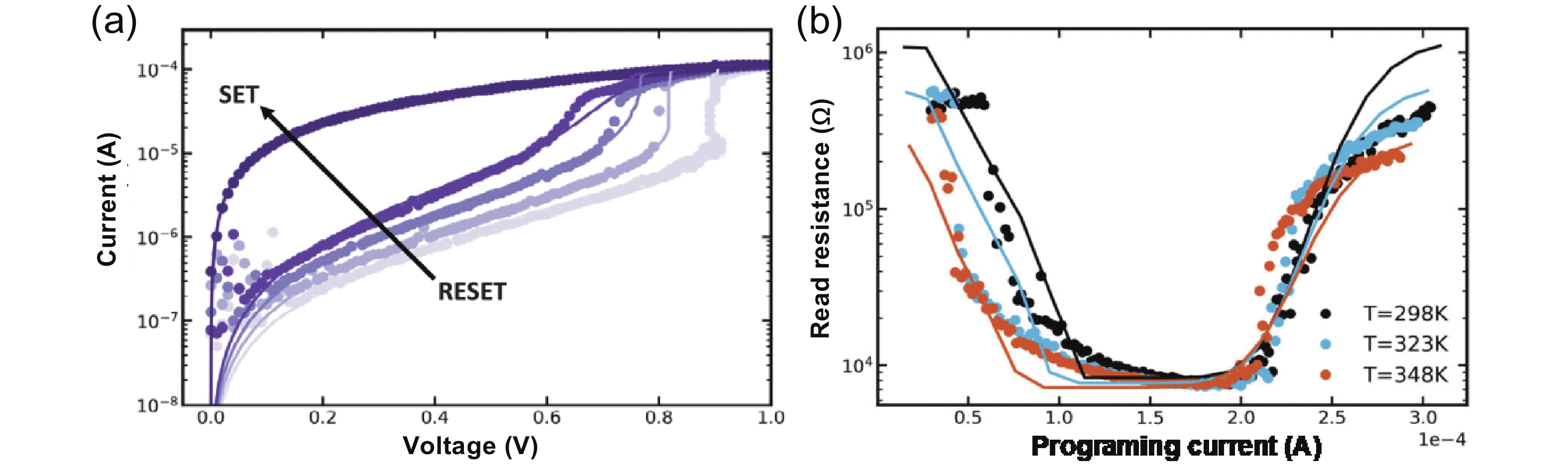
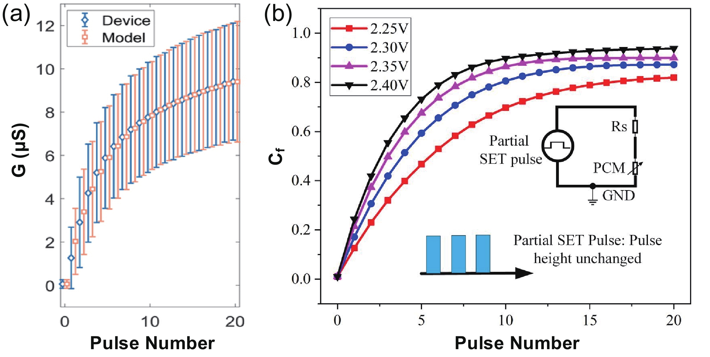
Phase change memory (PCM) attracts wide attention for the memory-centric computing and neuromorphic computing. For circuit and system designs, PCM compact models are mandatory and their status are reviewed in this work. Macro models and physics-based models have been proposed in different stages of the PCM technology developments. Compact modeling of PCM is indeed more complex than the transistor modeling due to their multi-physics nature including electrical, thermal and phase transition dynamics as well as their interactions. Realizations of the PCM operations including threshold switching, set and reset programming in these models are diverse, which also differs from the perspective of circuit simulations. For the purpose of efficient and reliable designs of the PCM technology, open issues and challenges of the compact modeling are also discussed.


J. Semicond.
2022, 43(2): 022101 doi: 10.1088/1674-4926/43/2/022101
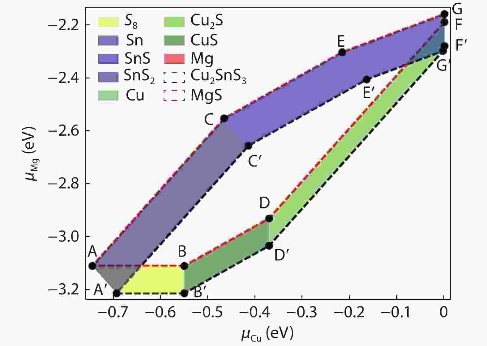
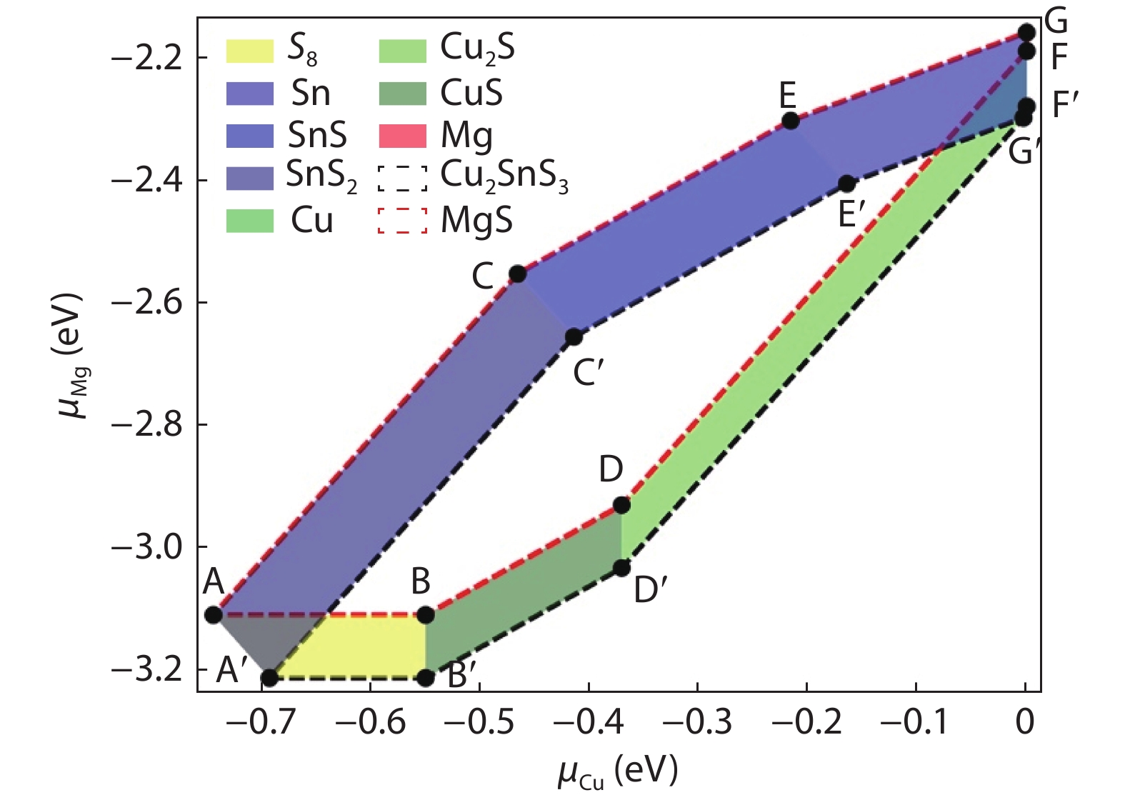
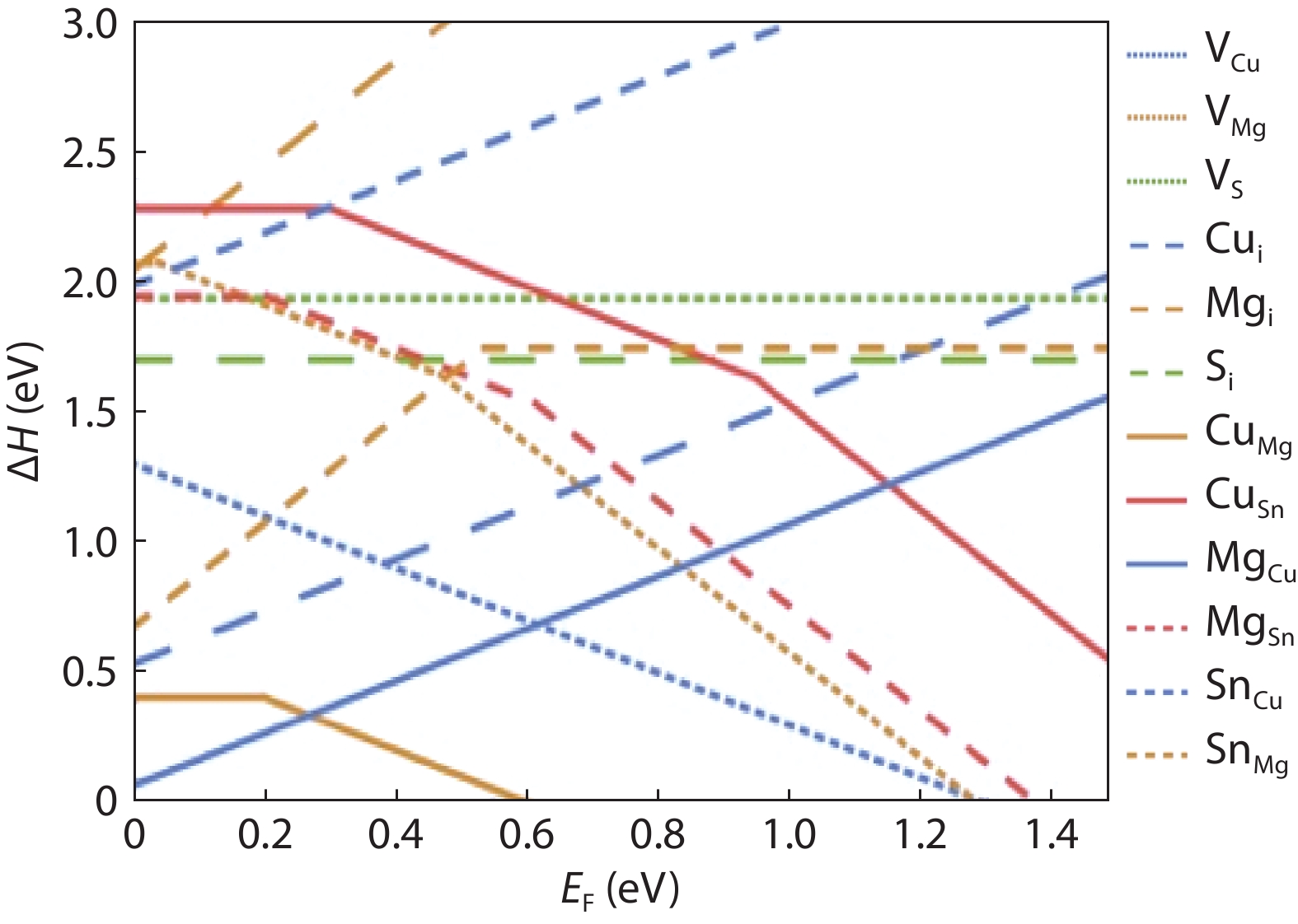
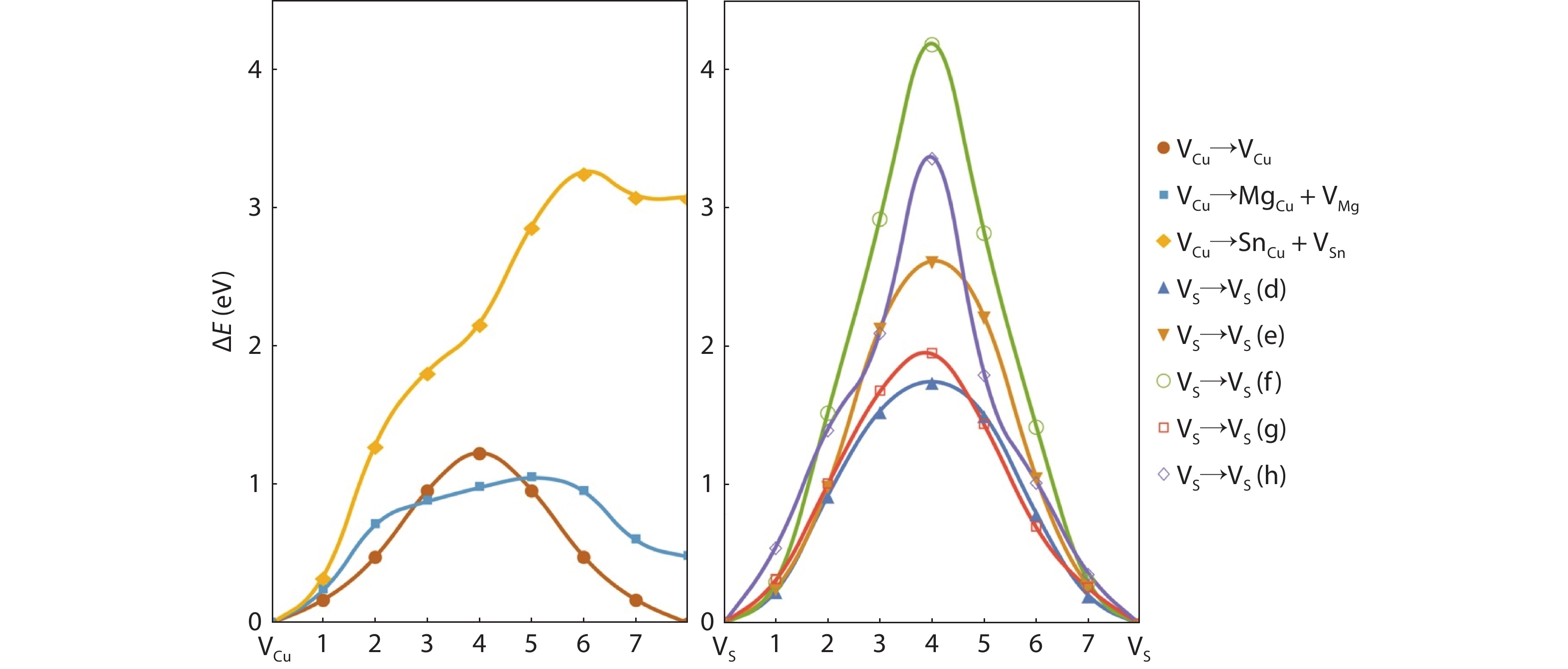
Cu2ZnSnS4 (CZTS) is a promising photovoltaic absorber material, however, efficiency is largely hindered by potential fluctuation and a band tailing problem due to the abundance of defect complexes and low formation energy of an intrinsic CuZn defect. Alternatives to CZTS by group I, II, or IV element replacement to circumvent this challenge has grown research interest. In this work, using a hybrid (HSE06) functional, we demonstrated the qualitative similarity of defect thermodynamics and electronic properties in Cu2MgSnS4 (CMTS) to CZTS. We show SnMg to be abundant when in Sn- and Cu-rich condition, which can be detrimental, while defect properties are largely similar to CZTS in Sn- and Cu-poor. Under Sn- and Cu-poor chemical potential, there is a general increase in formation energy in most defects except SnMg, CuMg remains as the main contribution to p-type carriers, and SnMg may be detrimental because of a deep defect level in the mid gap and the possibility of forming defect complex SnMg+MgSn. Vacancy diffusion is studied using generalized gradient approximation, and we find similar vacancy diffusion properties for Cu vacancy and lower diffusion barrier for Mg vacancy, which may reduce possible Cu-Mg disorder in CMTS. These findings further confirm the feasibility of CMTS as an alternative absorber material to CZTS and suggest the possibility for tuning defect properties of CZTS, which is crucial for high photovoltaic performance.


J. Semicond.
2022, 43(2): 022301 doi: 10.1088/1674-4926/43/2/022301
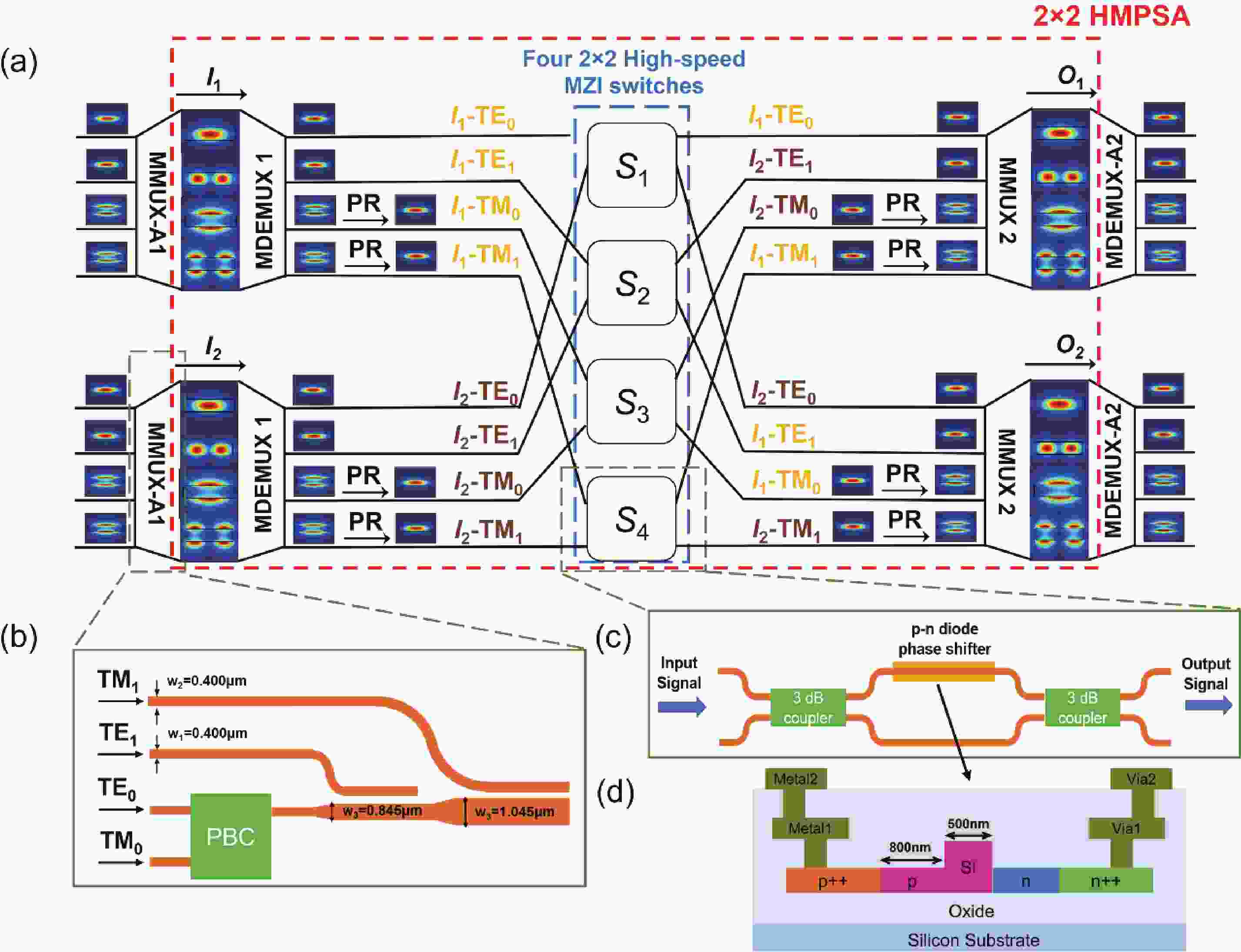
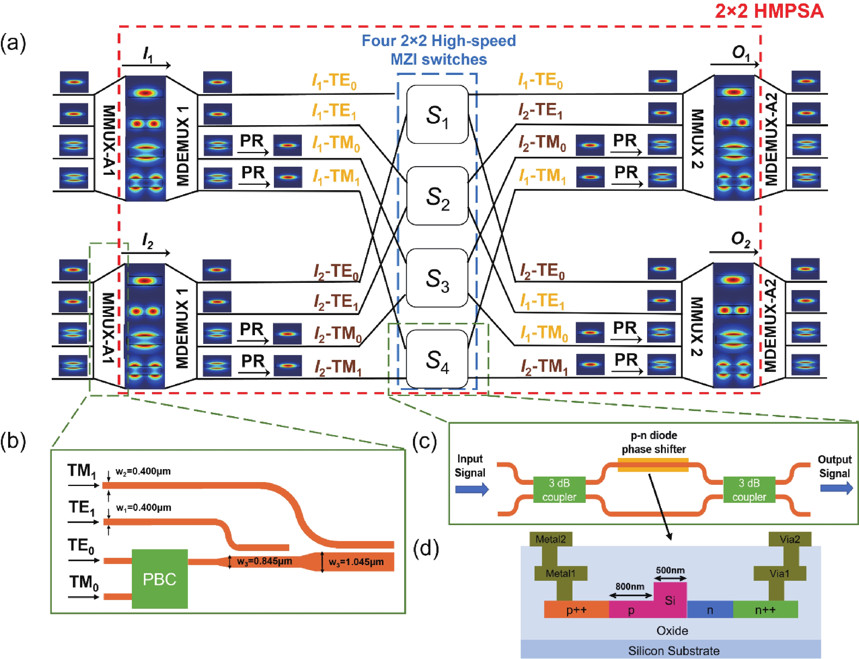
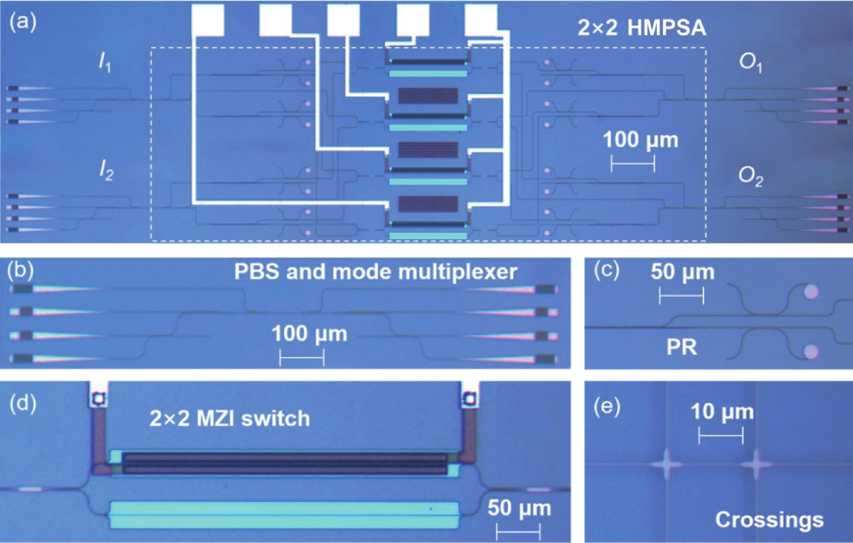
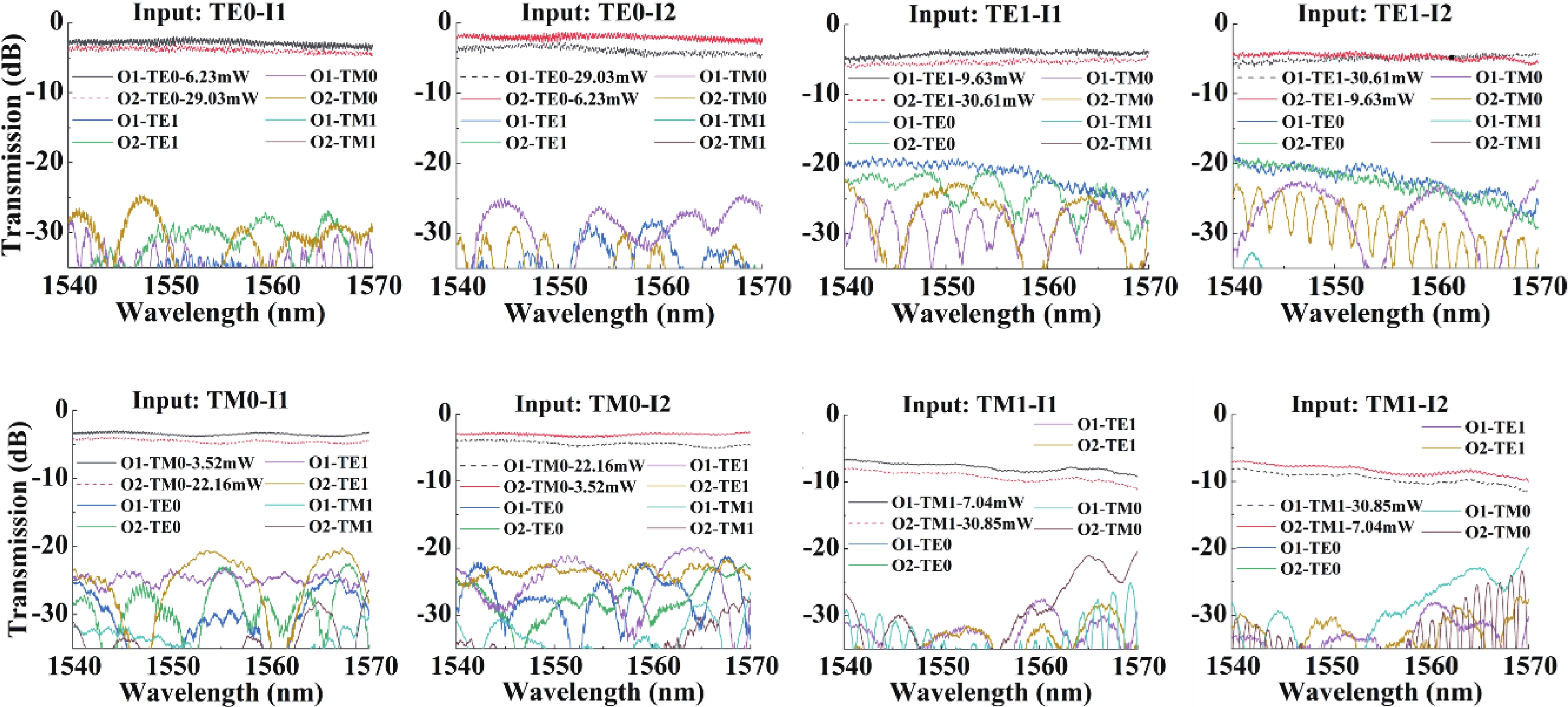
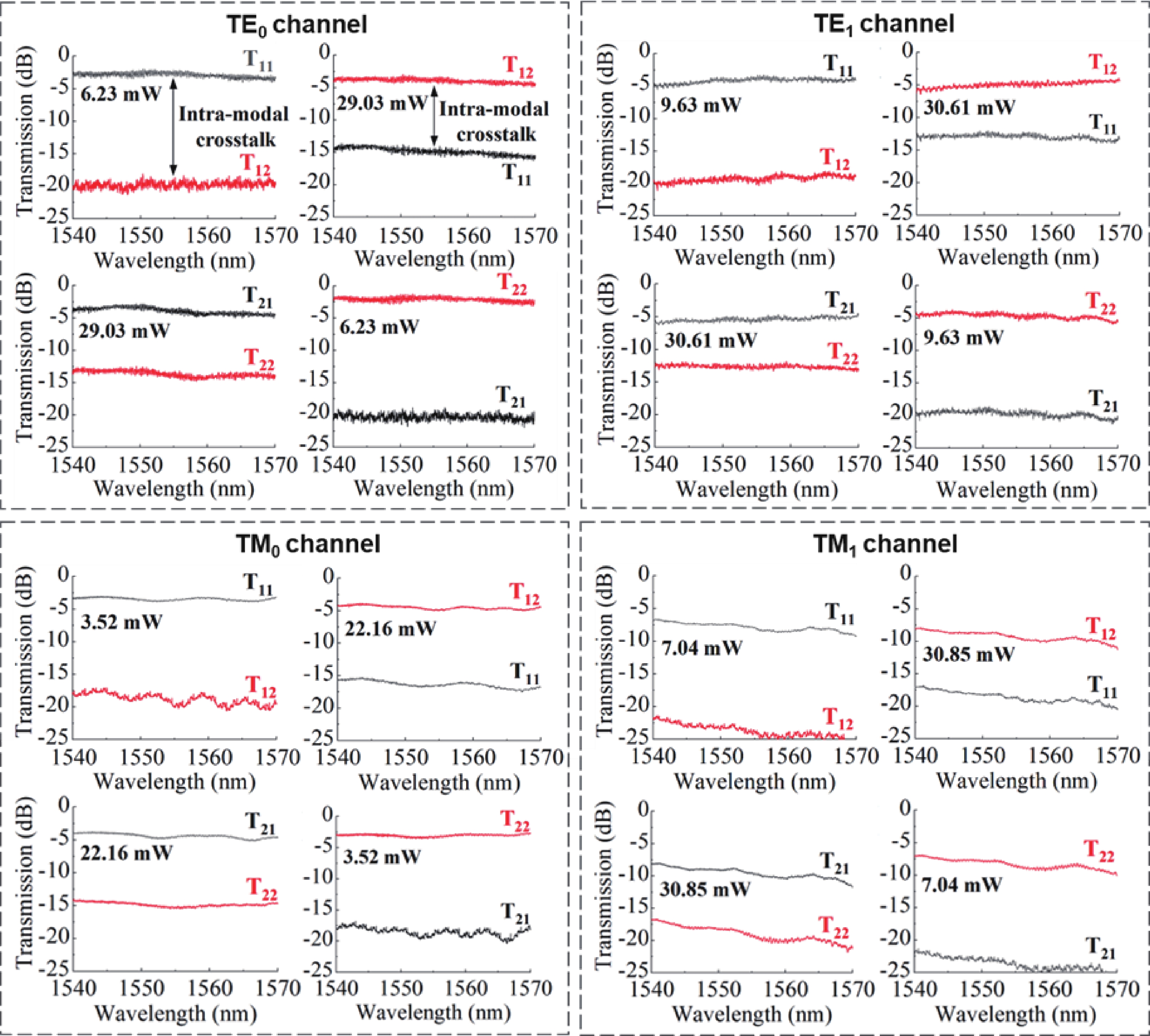
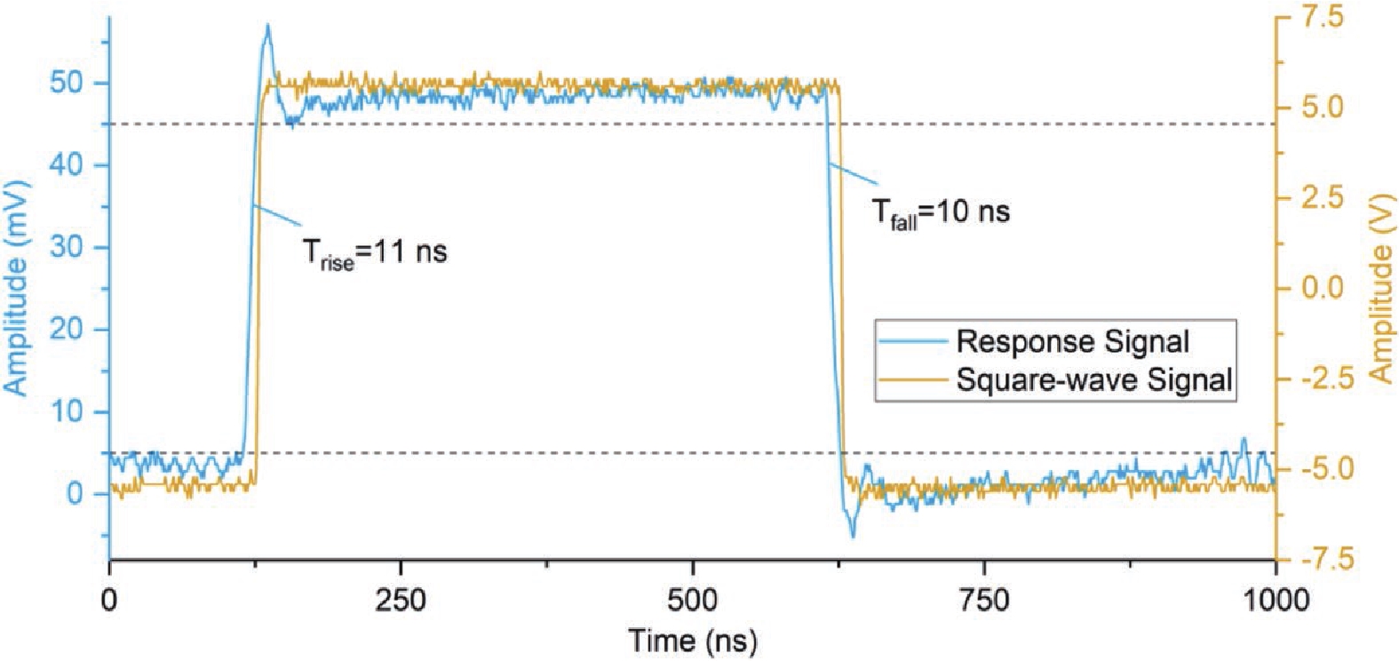
On-chip optical communications are growingly aiming at multimode operation together with mode-division multiplexing to further increase the transmission capacity. Optical switches, which are capable of optical signals switching at the nodes, play a key role in optical networks. We demonstrate a 2 × 2 electro-optic Mach–Zehnder interferometer-based mode- and polarization-selective switch fabricated by standard complementary metal–oxide–semiconductor process. An electro optic tuner based on a PN-doped junction in one of the Mach–Zehnder interferometer arms enables dynamic switching in 11 ns. For all the channels, the overall insertion losses and inter-modal crosstalk values are below 9.03 and –15.86 dB at 1550 nm, respectively.
J. Semicond.
2022, 43(2): 022801 doi: 10.1088/1674-4926/43/2/022801
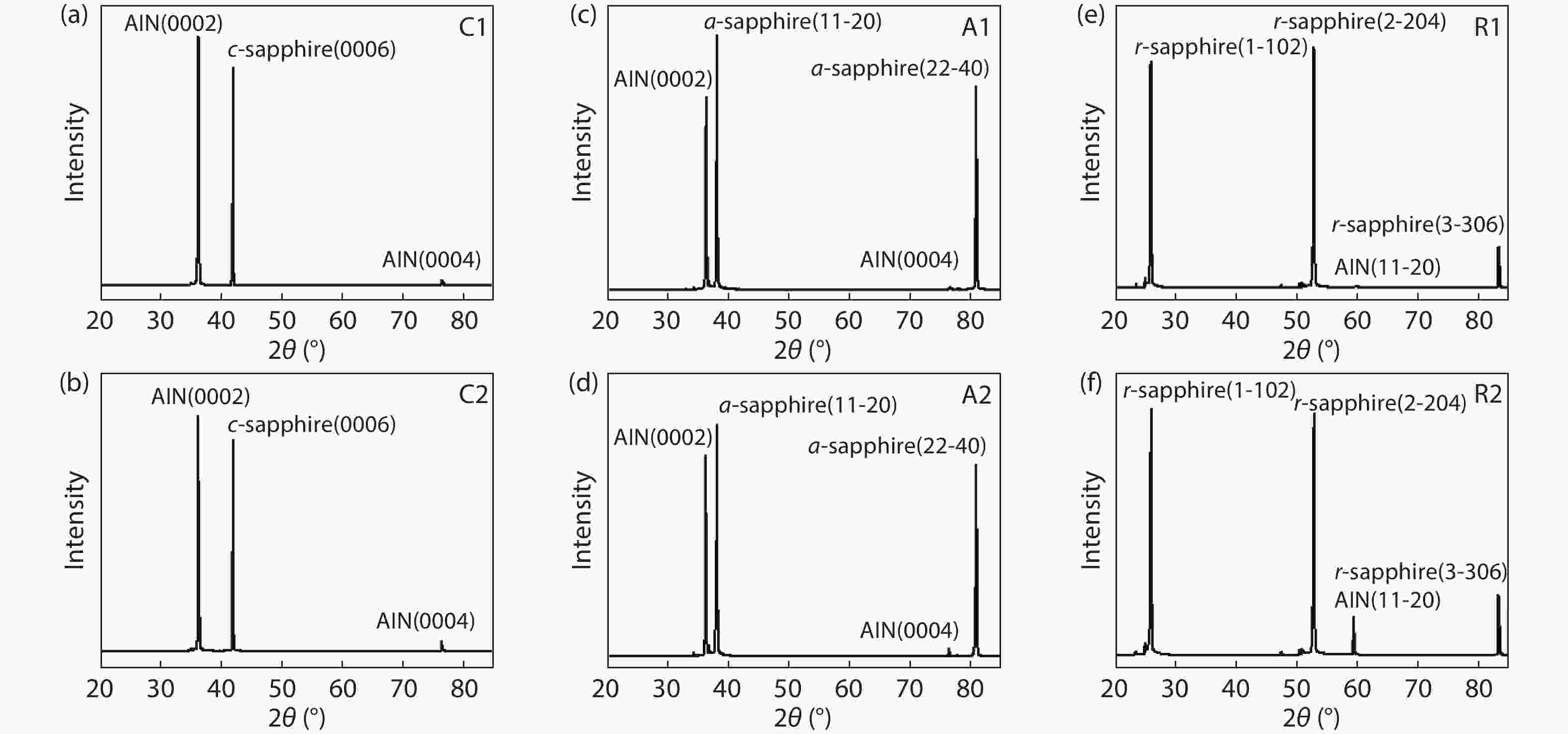
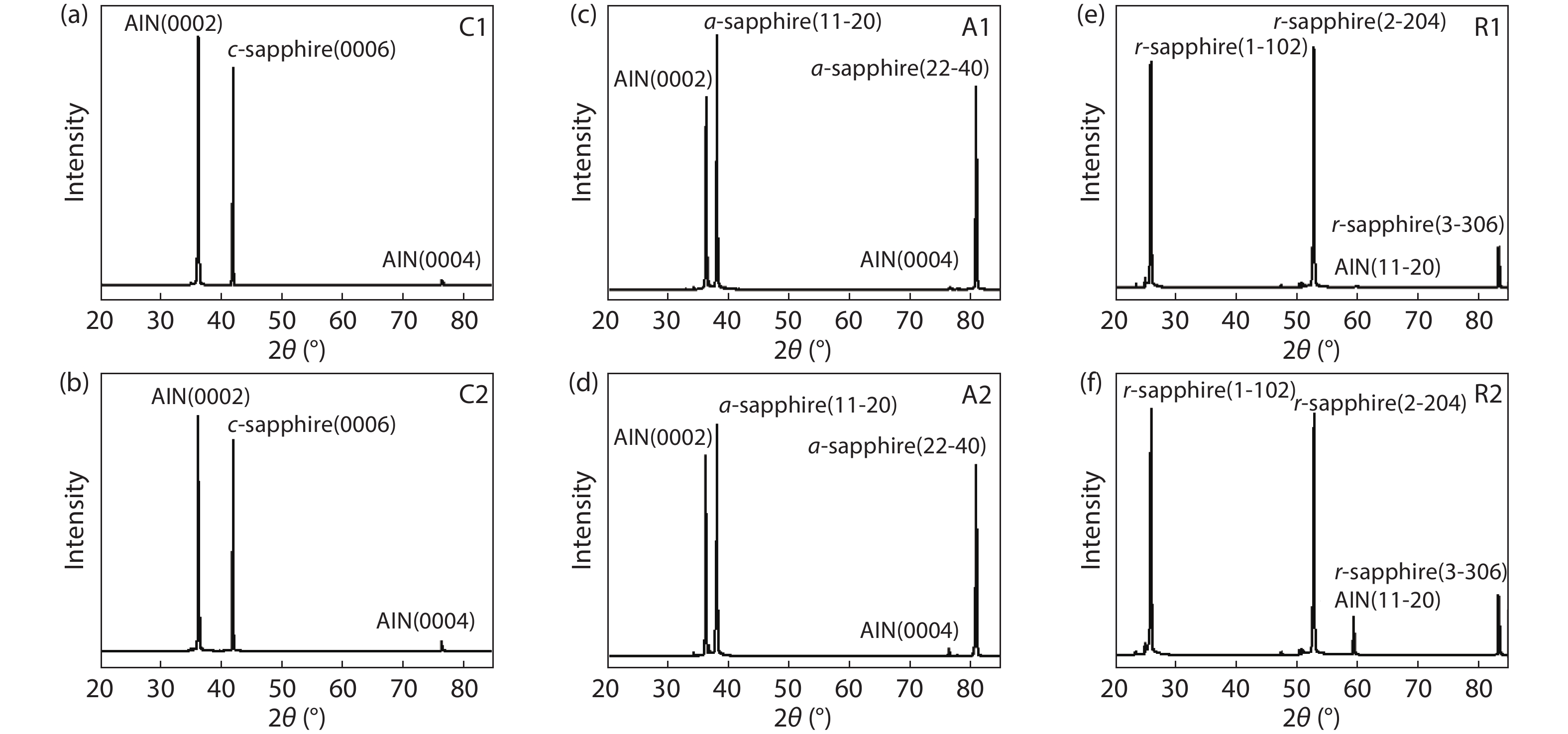
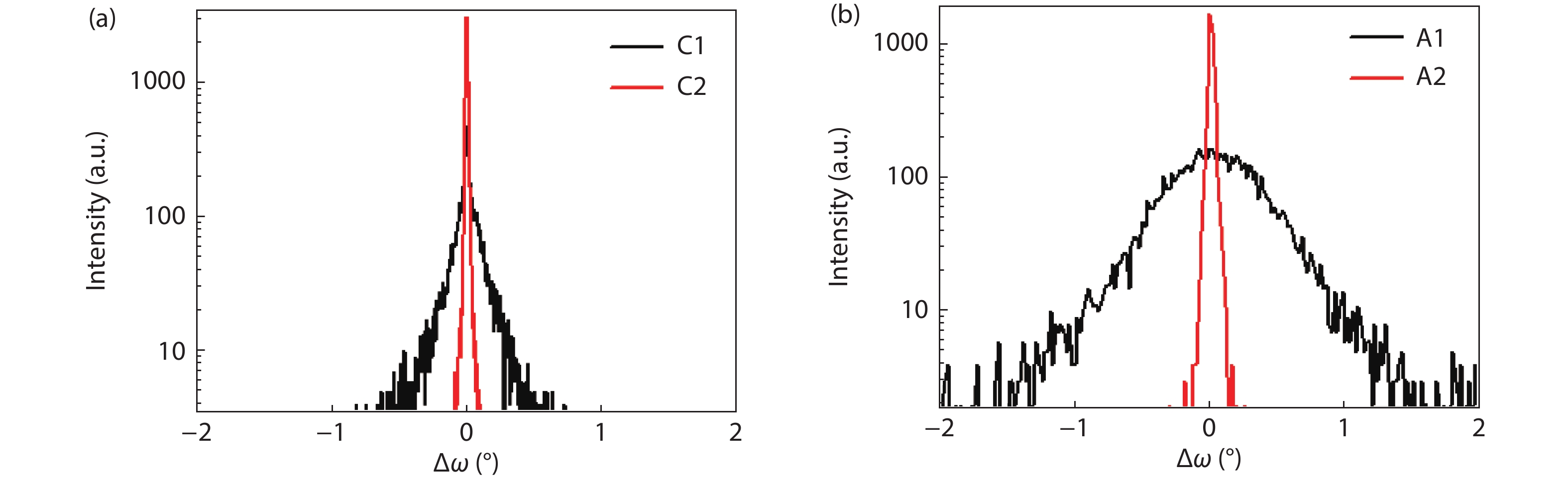
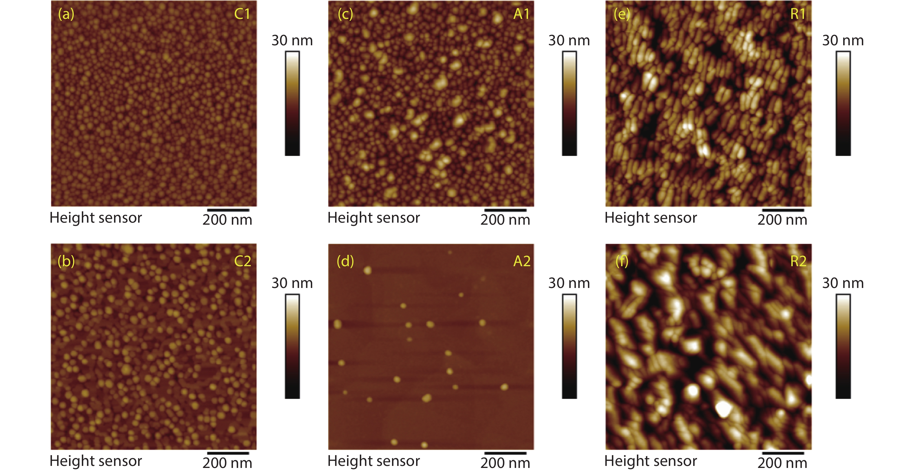
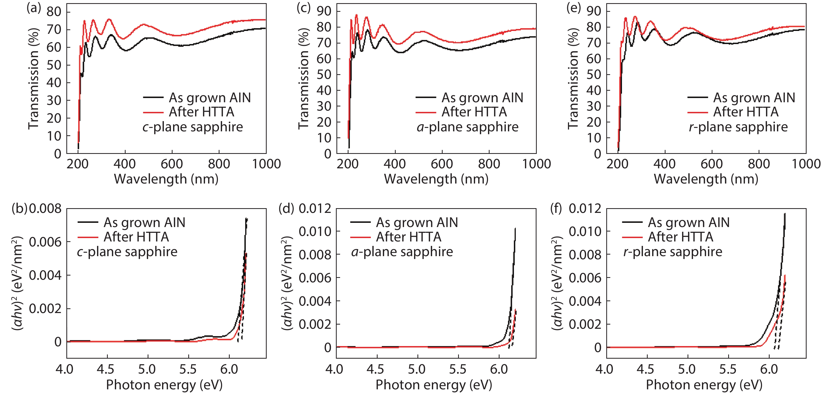
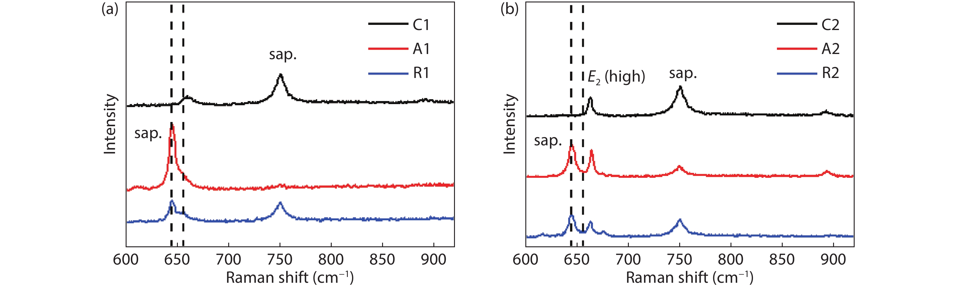
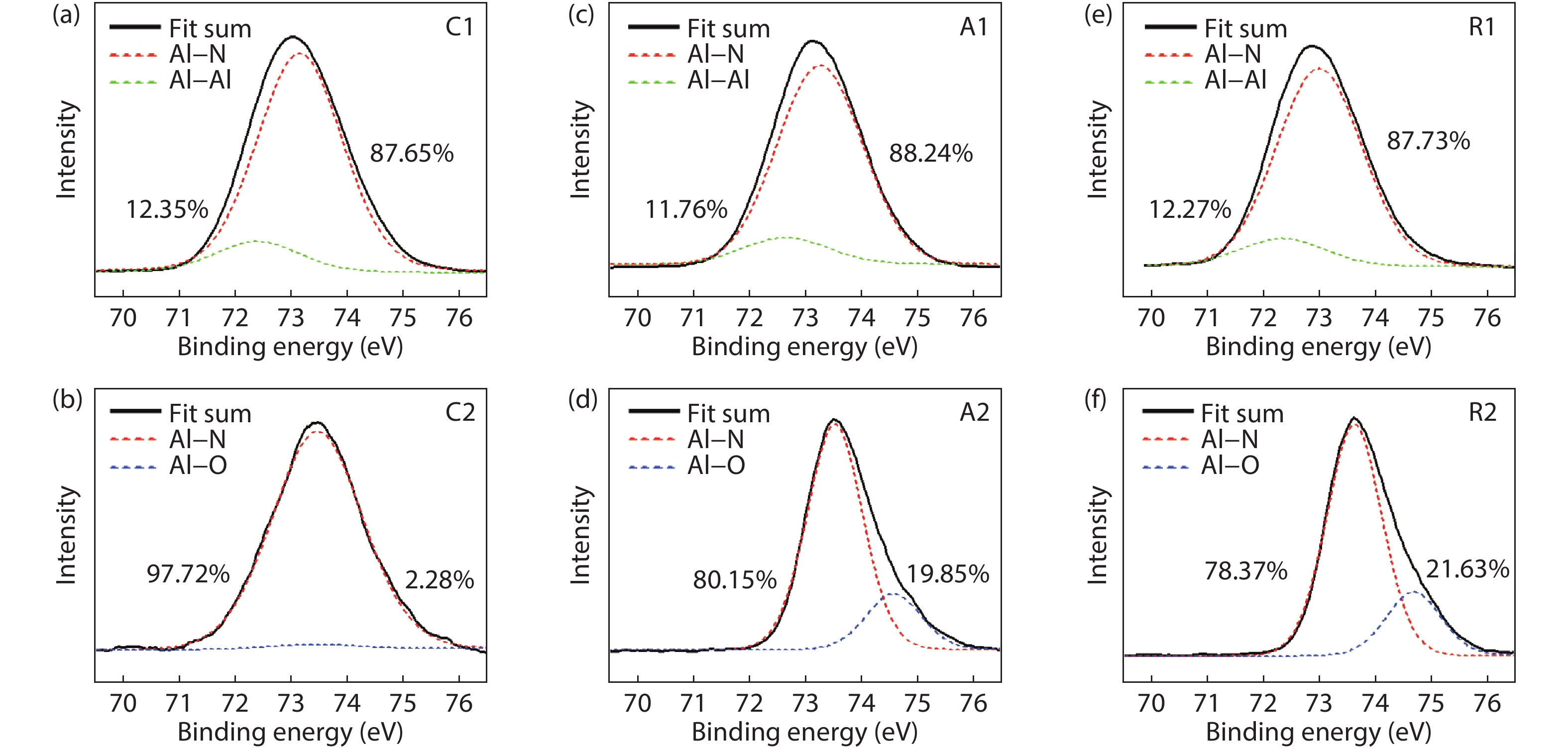
AlN thin films were deposited on c-, a- and r-plane sapphire substrates by the magnetron sputtering technique. The influence of high-temperature thermal annealing (HTTA) on the structural, optical properties as well as surface stoichiometry were comprehensively investigated. The significant narrowing of the (0002) diffraction peak to as low as 68 arcsec of AlN after HTTA implies a reduction of tilt component inside the AlN thin films, and consequently much-reduced dislocation densities. This is also supported by the appearance of E2(high) Raman peak and better Al–N stoichiometry after HTTA. Furthermore, the increased absorption edge after HTTA suggests a reduction of point defects acting as the absorption centers. It is concluded that HTTA is a universal post-treatment technique in improving the crystalline quality of sputtered AlN regardless of sapphire orientation.
J. Semicond.
2022, 43(2): 022802 doi: 10.1088/1674-4926/43/2/022802
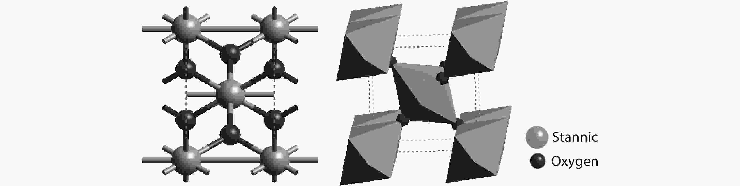
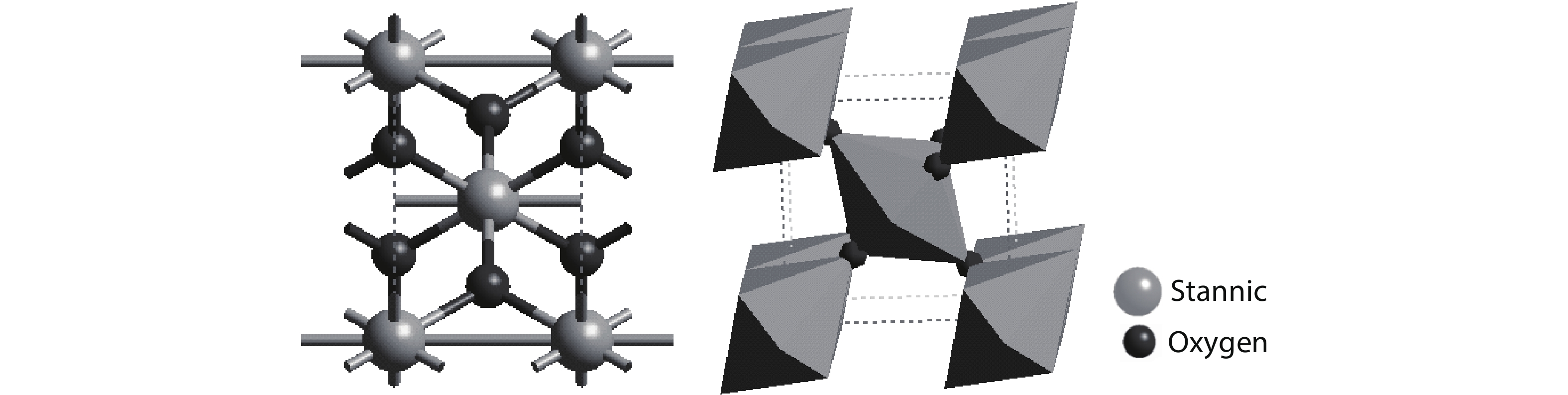
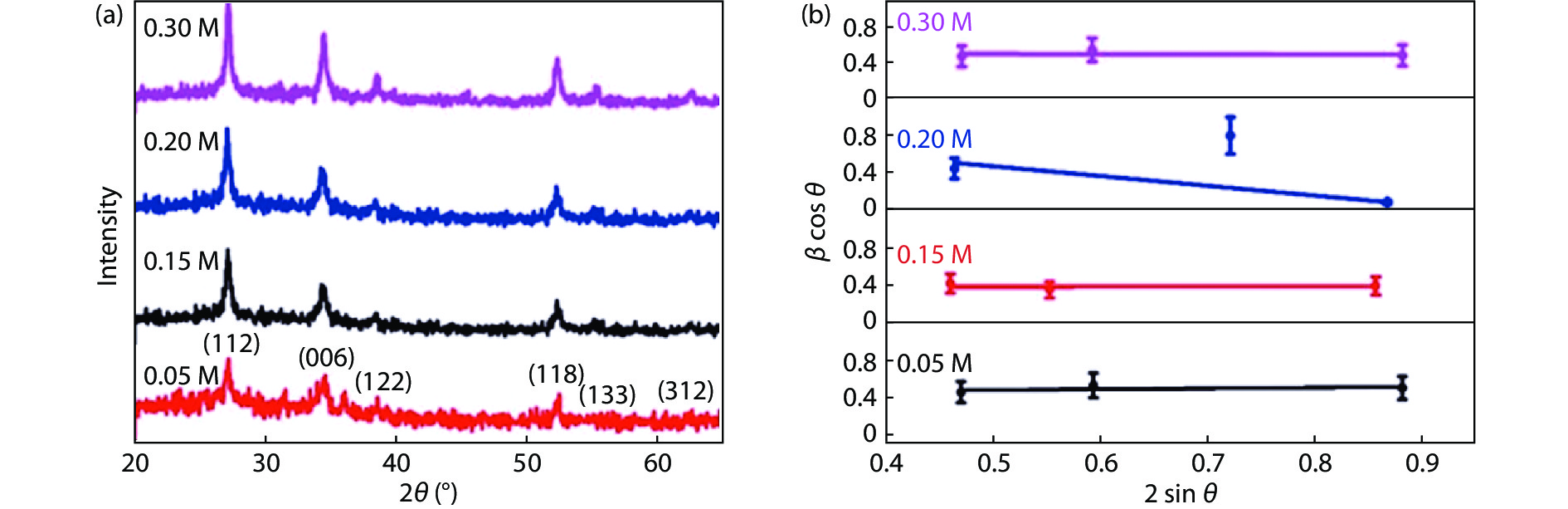
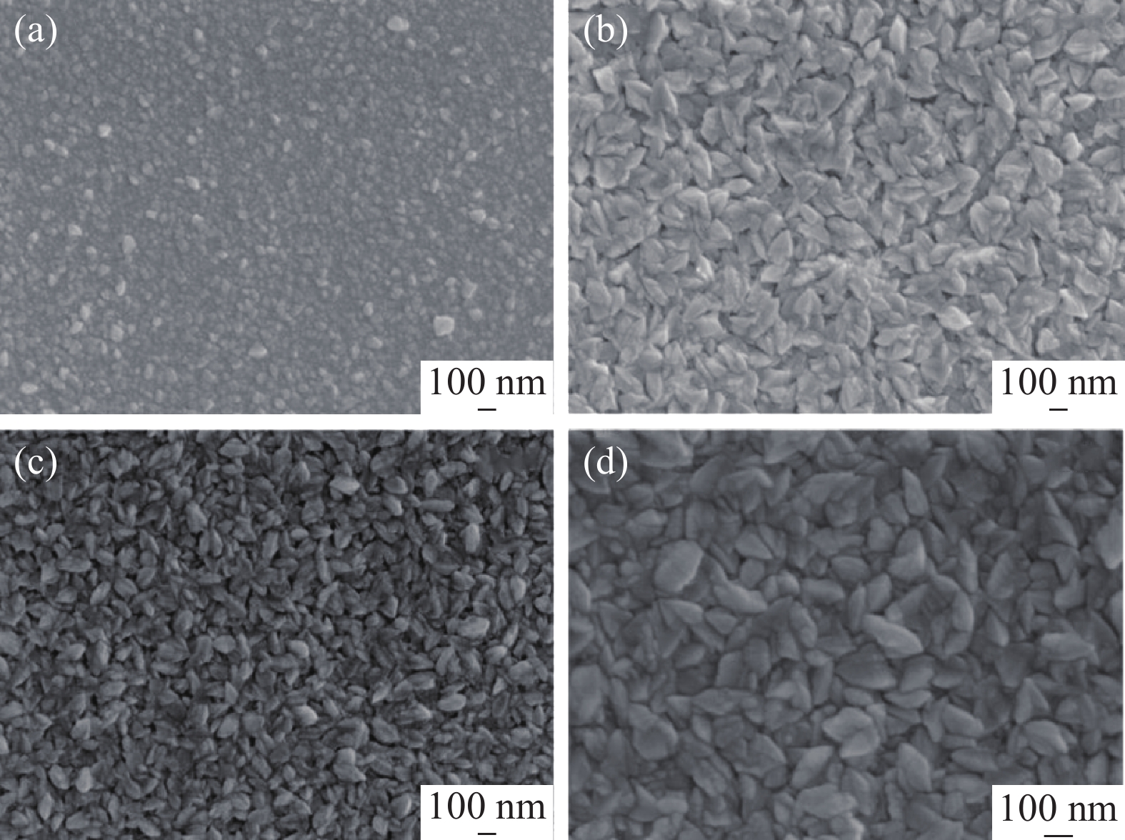
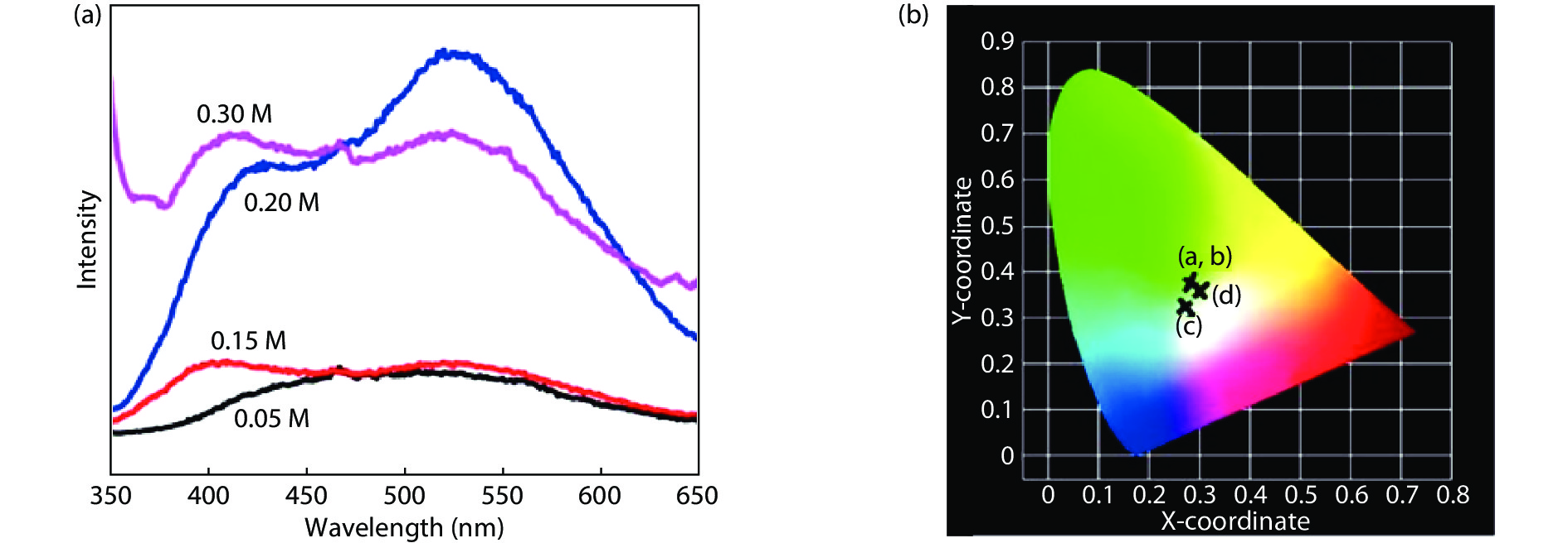
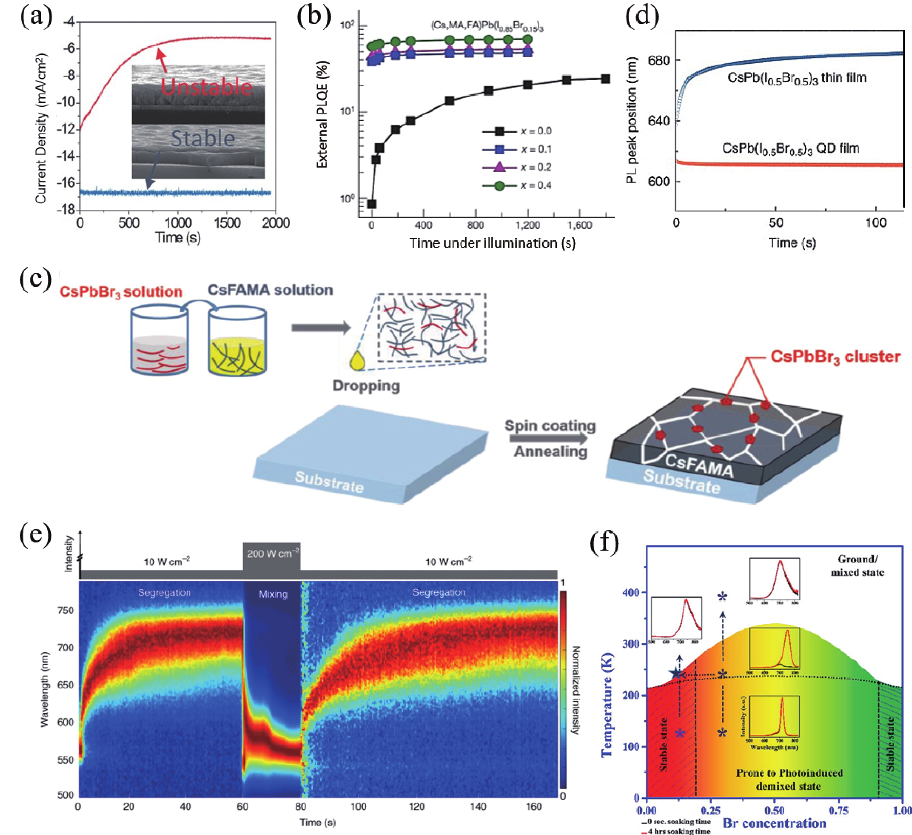
Highly transparent conductive stoichiometric nanocrystalline stannic oxide coatings were deposited onto Corning® EAGLE XG® slim glass substrates. Including each coating, it was deposited for various concentrations in the aerosol solution with the substrate temperature maintained at 623.15 K by an ultrasonic spray pyrolysis (USP) technique. Nitrogen was employed both as the solution carrier in addition to aerosol directing gas, maintaining its flow rates at 3500.0 and 500.0 mL/min, respectively. The coatings were polycrystalline, with preferential growth along the stannic oxide (112) plane, irrespective of the molarity content in the spray solution. The coating prepared at 0.2 M, a concentration in the aerosol solution, showed an average transmission of 60% in the visible light region spectrum with a maximum conductivity of 24.86 S/cm. The coatings deposited exhibited in the general photoluminescence spectrum emission colors of green, greenish white, and bluish white calculated on the intensities of the excitonic and oxygen vacancy defect level emissions.