Issue Browser
Volume 44, Issue 10,
Oct 2023

J. Semicond.
2023, 44(10): 101301 doi: 10.1088/1674-4926/44/10/101301

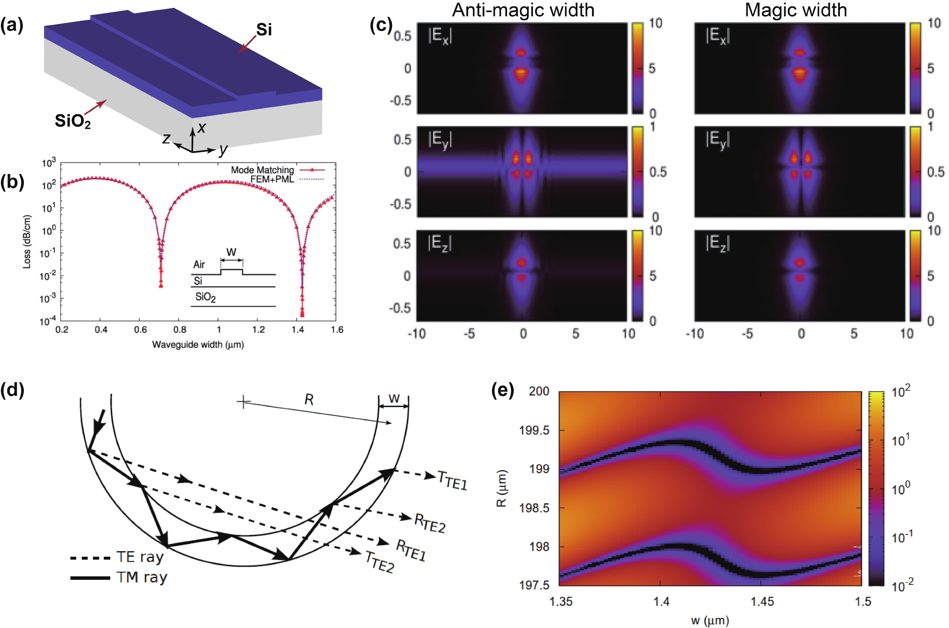
Photonic waveguides are the most fundamental element for photonic integrated circuits (PICs). Waveguide properties, such as propagation loss, modal areas, nonlinear coefficients, etc., directly determine the functionalities and performance of PICs. Recently, the emerging waveguides with bound states in the continuum (BICs) have opened new opportunities for PICs because of their special properties in resonance and radiation. Here, we review the recent progress of PICs composed of waveguides with BICs. First, fundamentals including background physics and design rules of a BIC-based waveguide will be introduced. Next, two types of BIC-based waveguide structures, including shallowly etched dielectric and hybrid waveguides, will be presented. Lastly, the challenges and opportunities of PICs with BICs will be discussed.


J. Semicond.
2023, 44(10): 103101 doi: 10.1088/1674-4926/44/10/103101

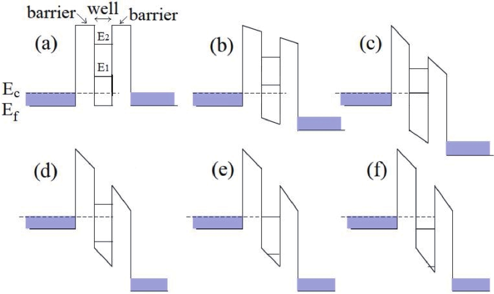
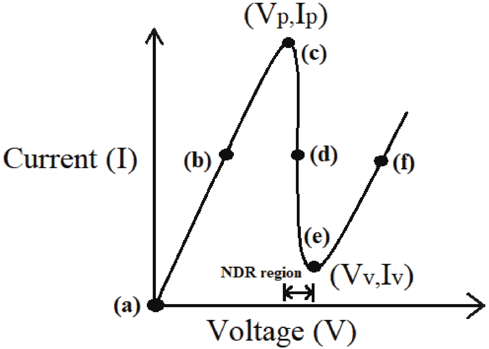
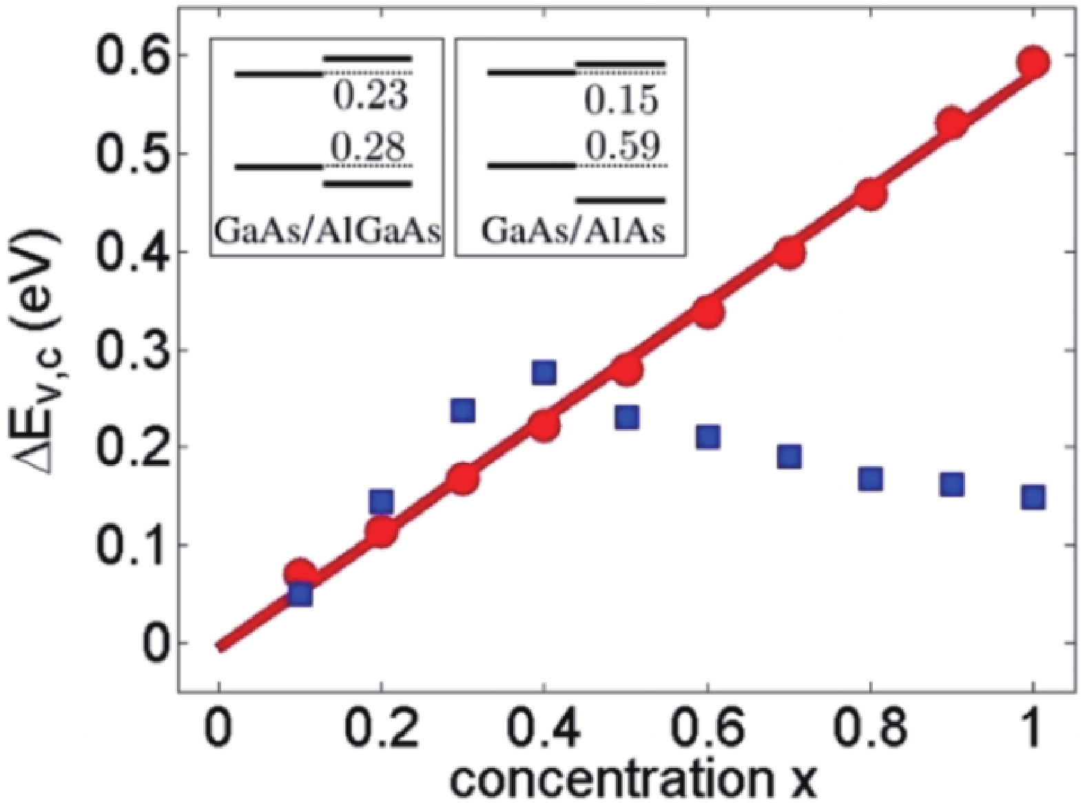
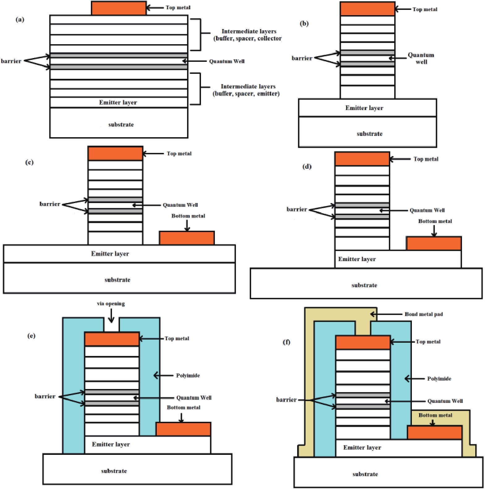
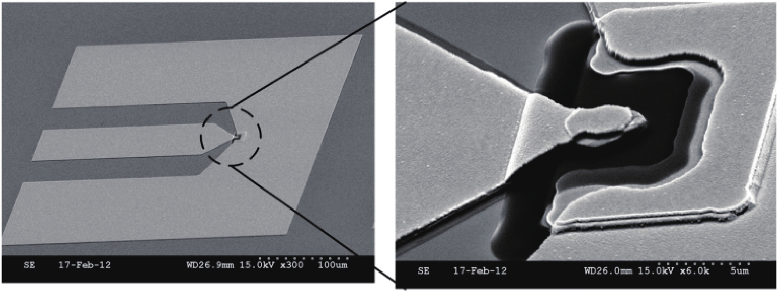
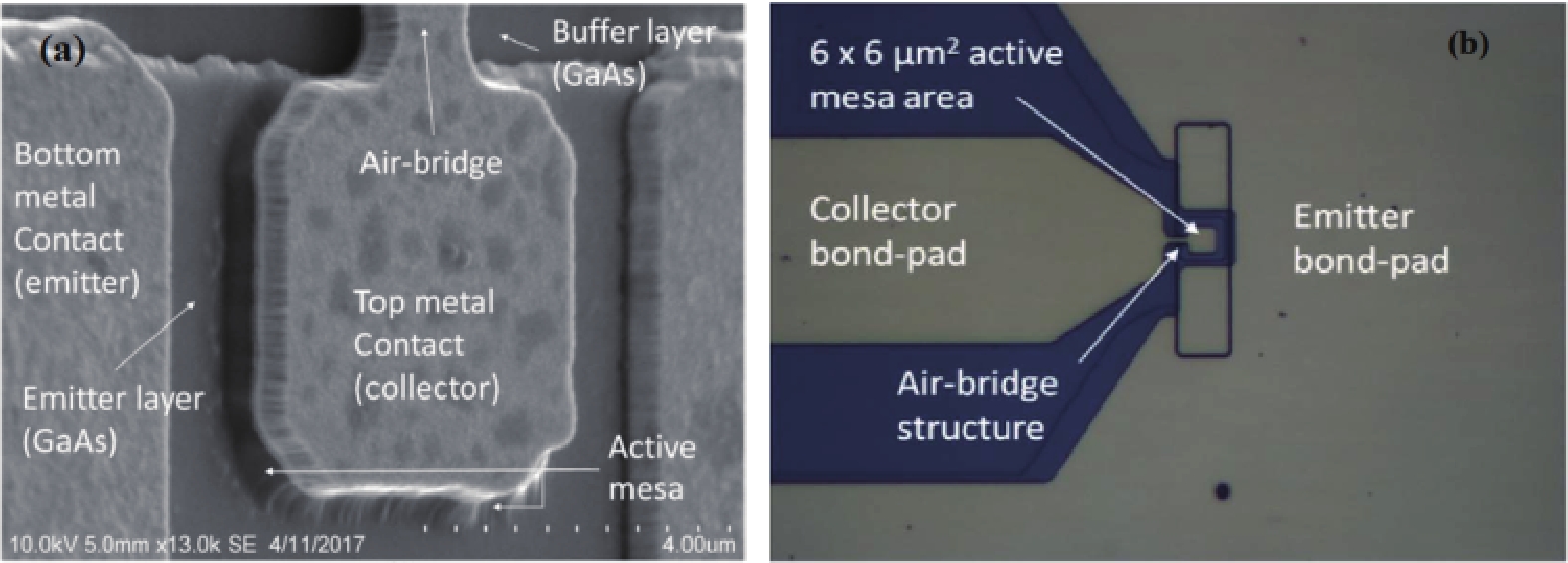
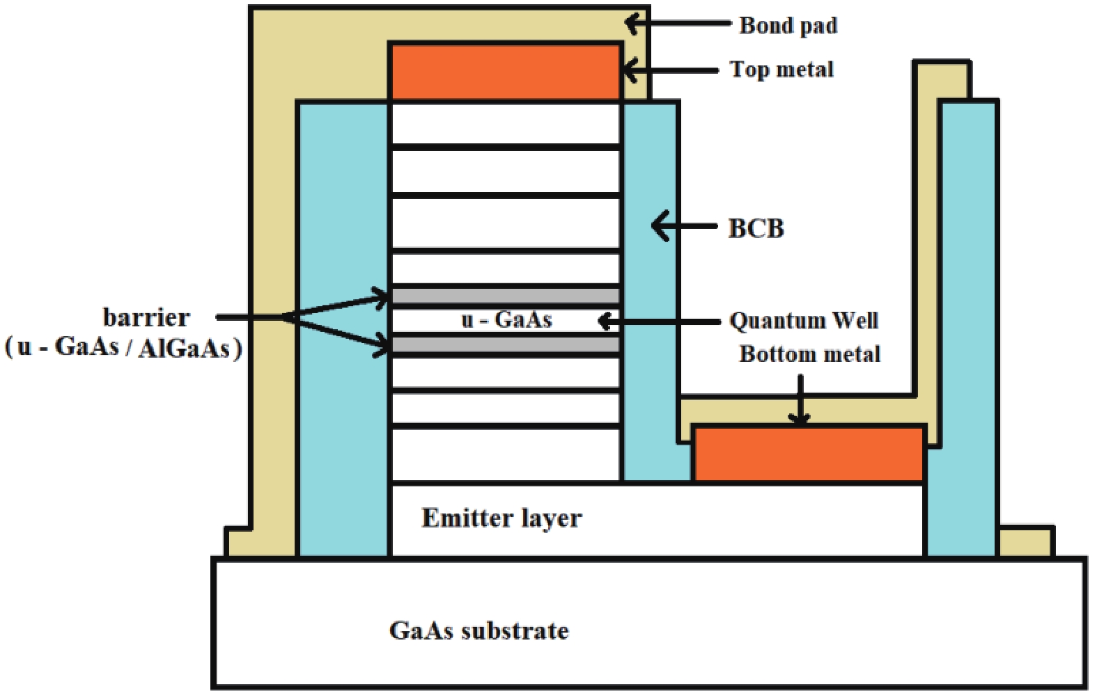
This review article discusses the development of gallium arsenide (GaAs)-based resonant tunneling diodes (RTD) since the 1970s. To the best of my knowledge, this article is the first review of GaAs RTD technology which covers different epitaxial-structure design, fabrication techniques, and characterizations for various application areas. It is expected that the details presented here will help the readers to gain a perspective on the previous accomplishments, as well as have an outlook on the current trends and future developments in GaAs RTD research.
J. Semicond.
2023, 44(10): 102001 doi: 10.1088/1674-4926/44/10/102001
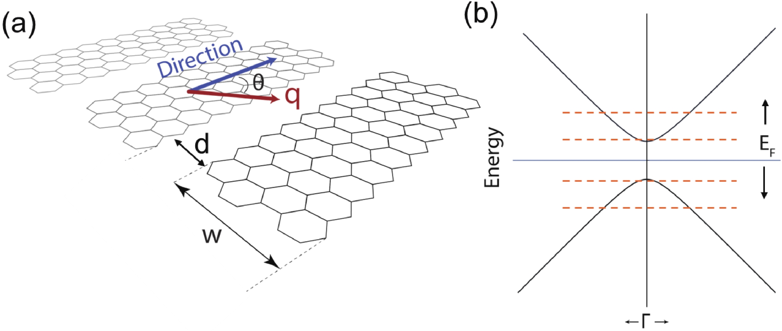
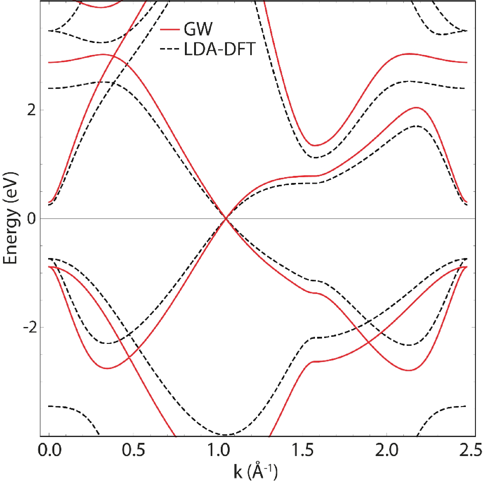
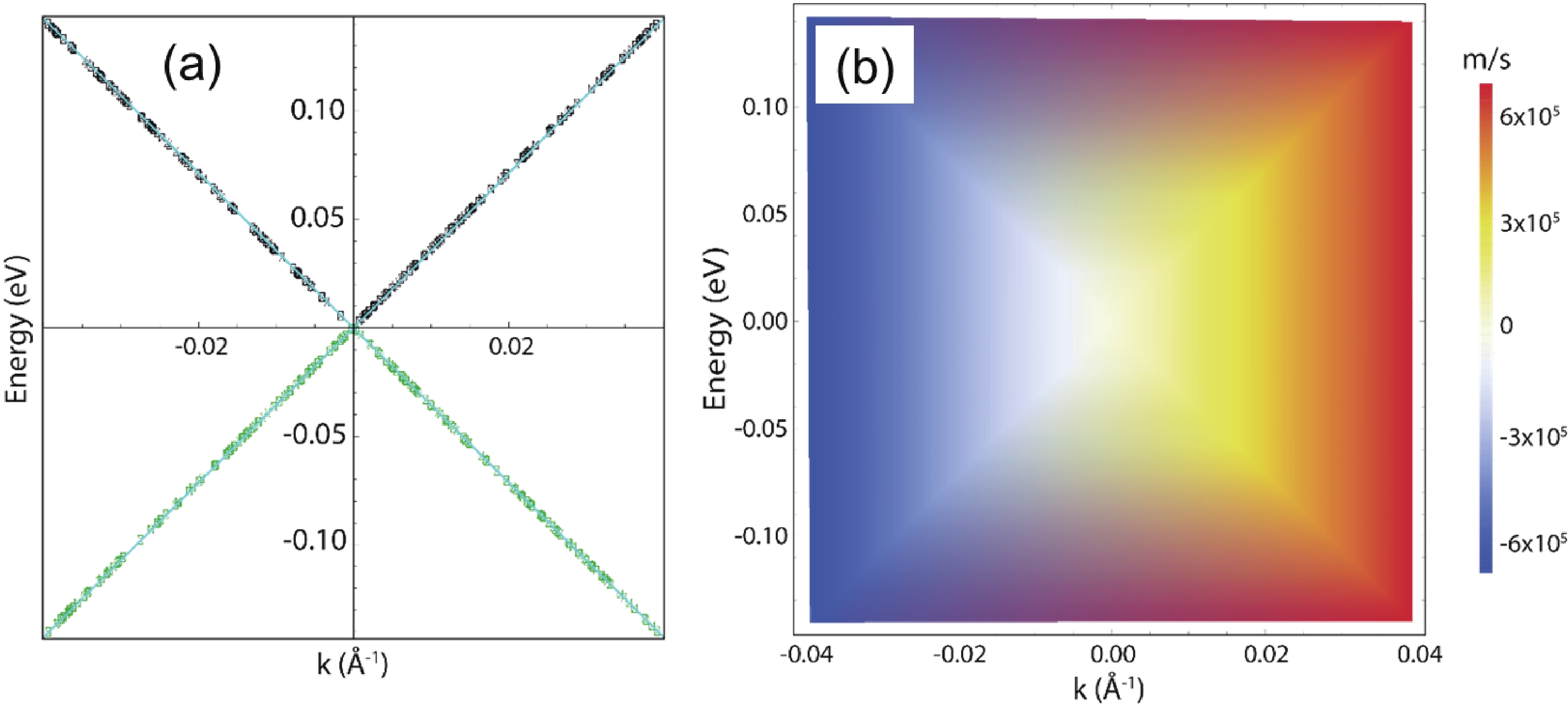
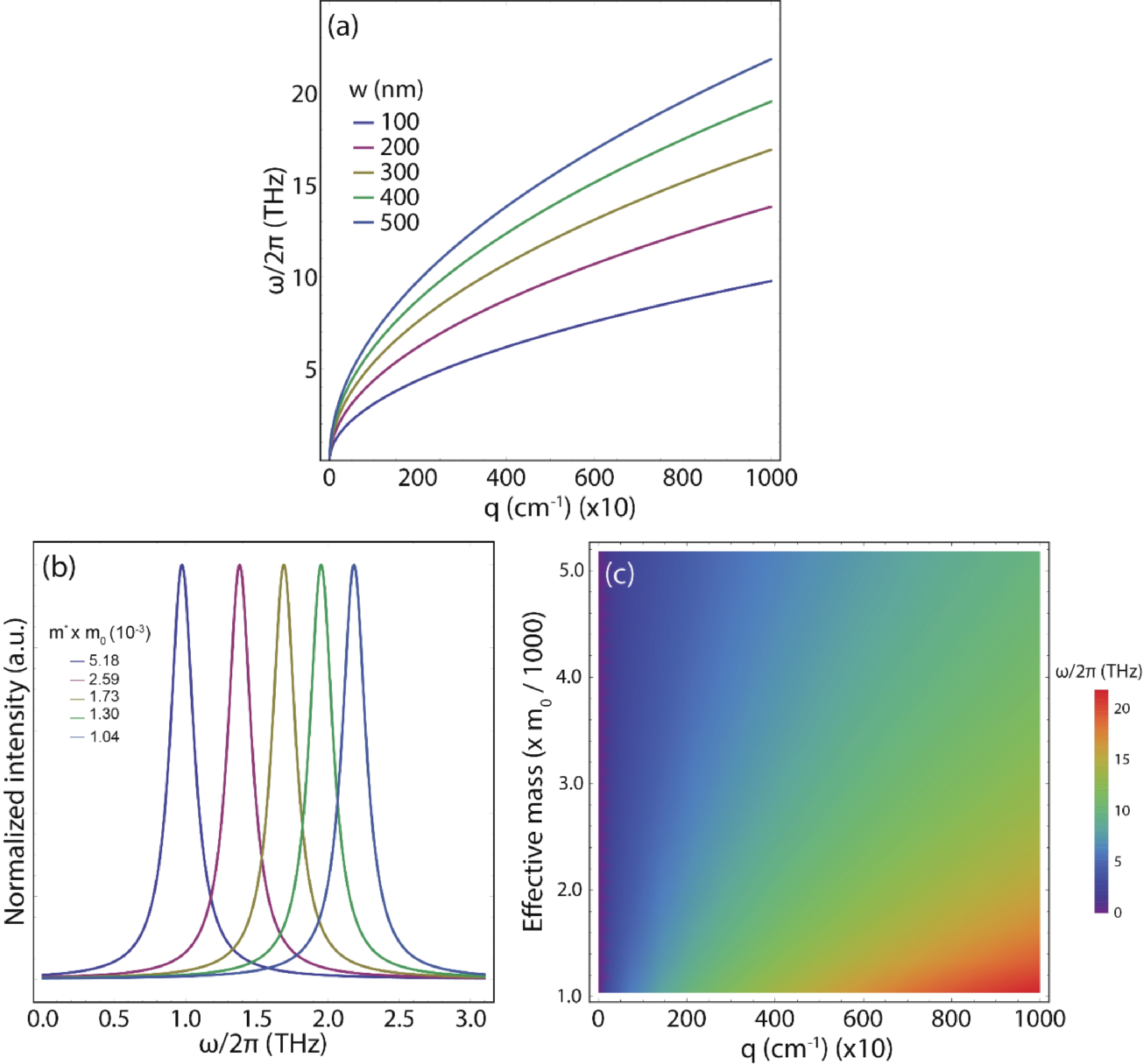
Germanene nanostrips (GeNSs) have garnered significant attention in modern semiconductor technology due to their exceptional physical characteristics, positioning them as promising candidates for a wide range of applications. GeNSs exhibit a two-dimensional (buckled) honeycomb-like lattice, which is similar to germanene but with controllable bandgaps. The modeling of GeNSs is essential for developing appropriate synthesis methods as it enables understanding and controlling the growth process of these systems. Indeed, one can adjust the strip width, which in turn can tune the bandgap and plasmonic response of the material to meet specific device requirements. In this study, the objective is to investigate the electronic behavior and THz plasmon features of GeNSs (≥100 nm wide). A semi-analytical model based on the charge-carrier velocity of freestanding germanene is utilized for this purpose. The charge-carrier velocity of freestanding germanene is determined through the GW approximation (${v}_{\mathrm{F}}=0.702 \times {10}^{6} $ m·s−1). Within the width range of 100 to 500 nm, GeNSs exhibit narrow bandgaps, typically measuring only a few meV. Specifically, upon analysis, it was found that the bandgaps of the investigated GeNSs ranged between 29 and 6 meV. As well, these nanostrips exhibit $ \sqrt{q} $-like plasmon dispersions, with their connected plasmonic frequency (≤30 THz) capable of being manipulated by varying parameters such as strip width, excitation plasmon angle, and sample quality. These manipulations can lead to frequency variations, either increasing or decreasing, as well as shifts towards larger momentum values. The outcomes of our study serve as a foundational motivation for future experiments, and further confirmation is needed to validate the reported results.


J. Semicond.
2023, 44(10): 102101 doi: 10.1088/1674-4926/44/10/102101
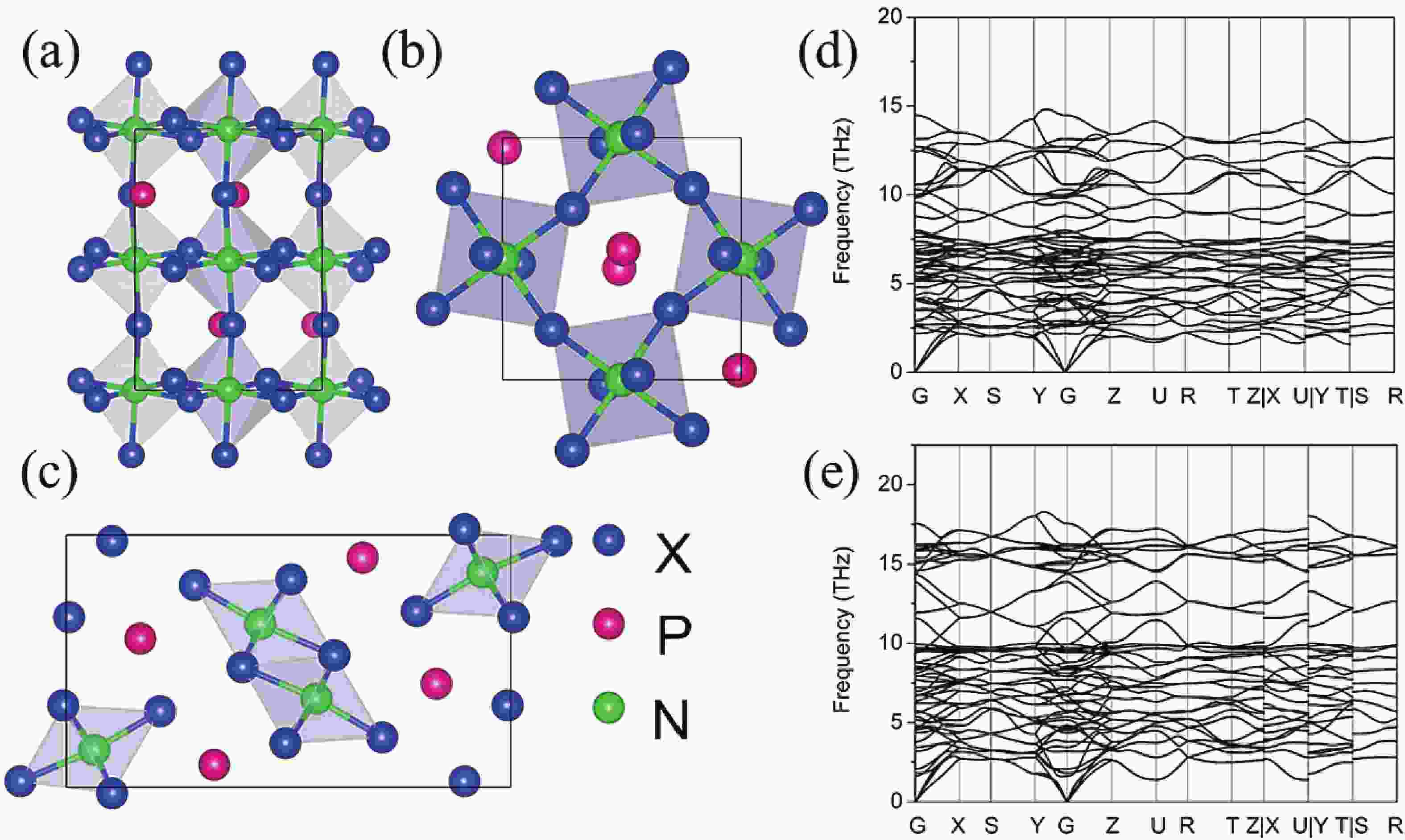
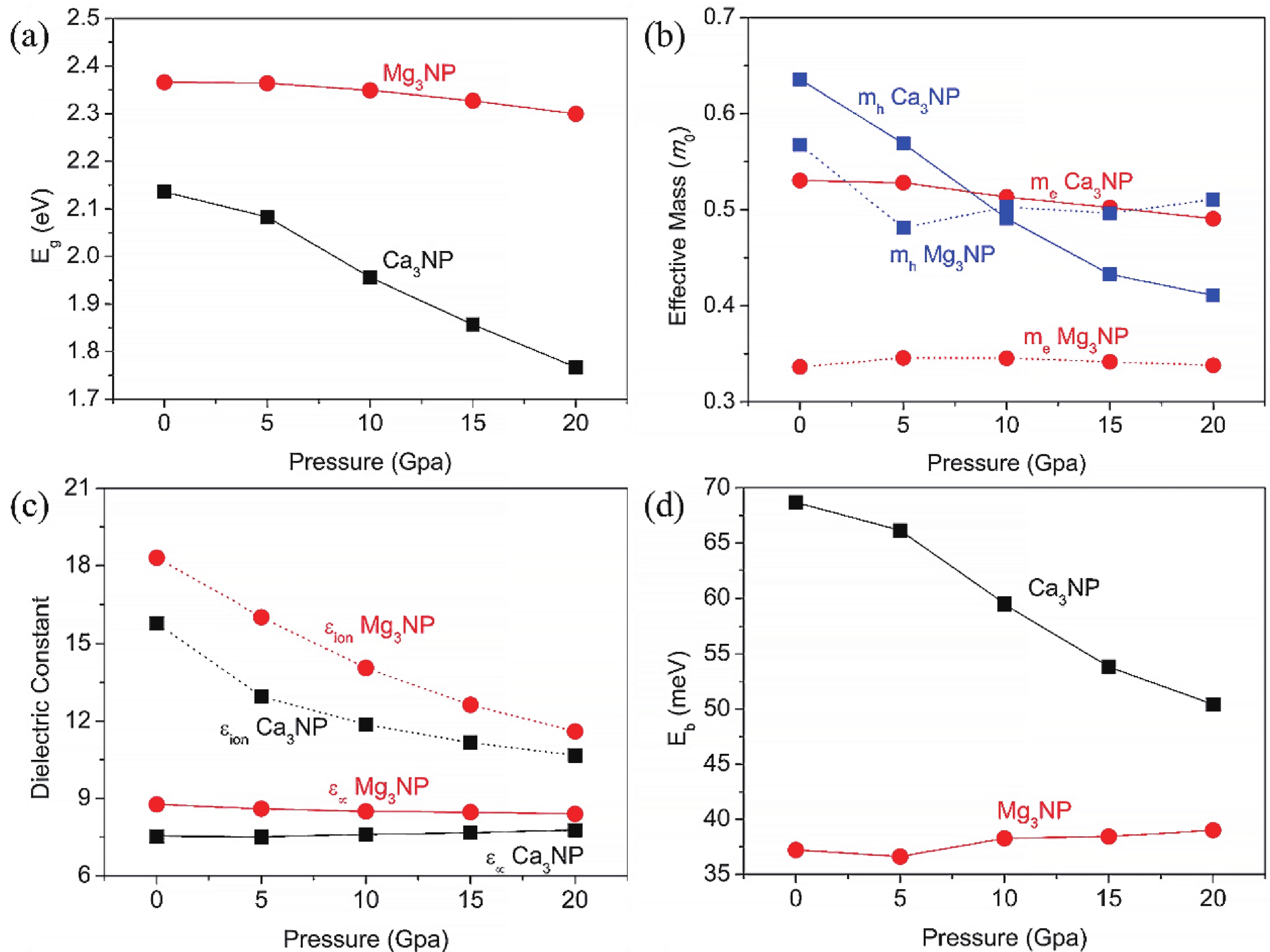
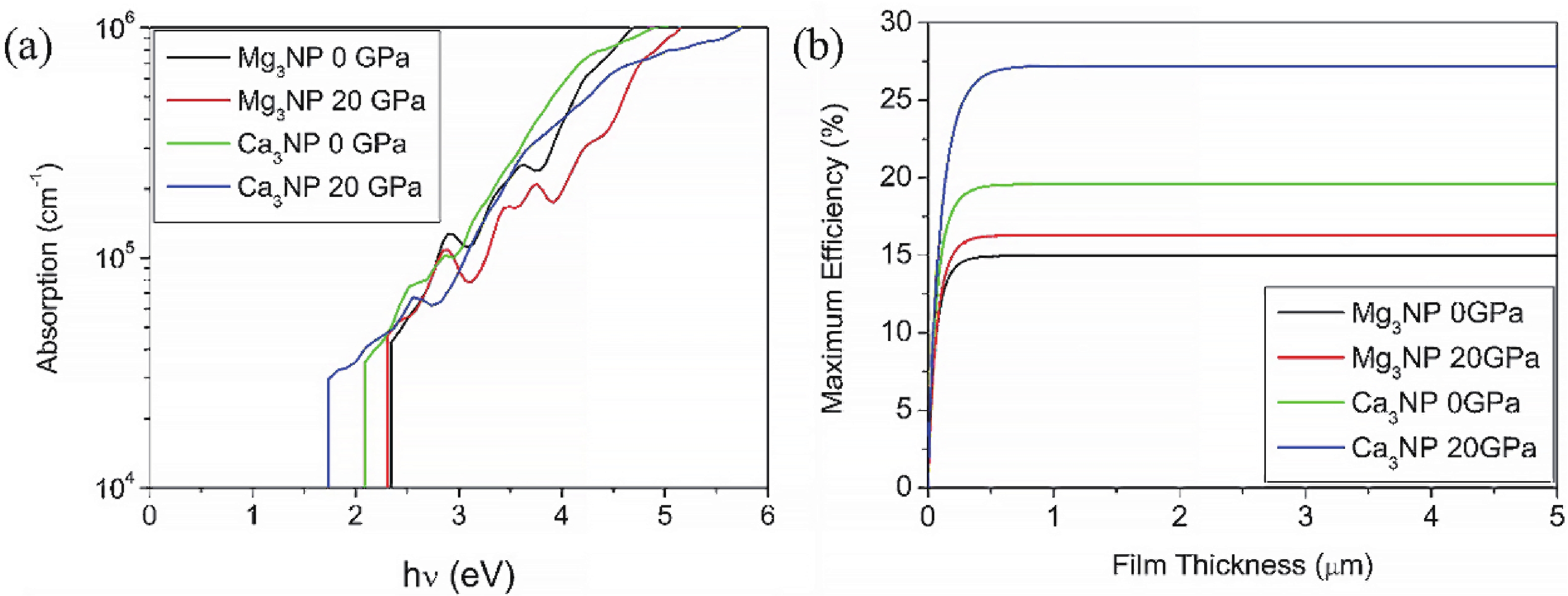
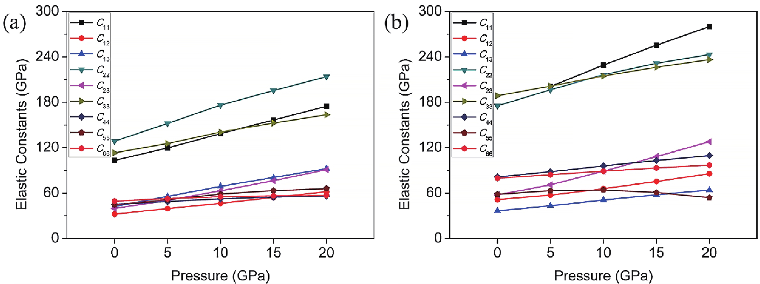
Hydrostatic pressure provides an efficient way to tune and optimize the properties of solid materials without changing their composition. In this work, we investigate the electronic, optical, and mechanical properties of antiperovskite X3NP (X2+ = Ca, Mg) upon compression by first-principles calculations. Our results reveal that the system is anisotropic, and the lattice constant a of X3NP exhibits the fastest rate of decrease upon compression among the three directions, which is different from the typical Pnma phase of halide and chalcogenide perovskites. Meanwhile, Ca3NP has higher compressibility than Mg3NP due to its small bulk modulus. The electronic and optical properties of Mg3NP show small fluctuations upon compression, but those of Ca3NP are more sensitive to pressure due to its higher compressibility and lower unoccupied 3d orbital energy. For example, the band gap, lattice dielectric constant, and exciton binding energy of Ca3NP decrease rapidly as the pressure increases. In addition, the increase in pressure significantly improves the optical absorption and theoretical conversion efficiency of Ca3NP. Finally, the mechanical properties of X3NP are also increased upon compression due to the reduction in bond length, while inducing a brittle-to-ductile transition. Our research provides theoretical guidance and insights for future experimental tuning of the physical properties of antiperovskite semiconductors by pressure.


J. Semicond.
2023, 44(10): 102301 doi: 10.1088/1674-4926/44/10/102301
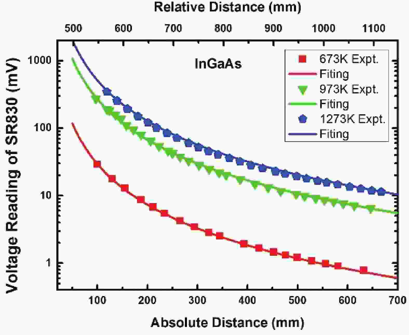
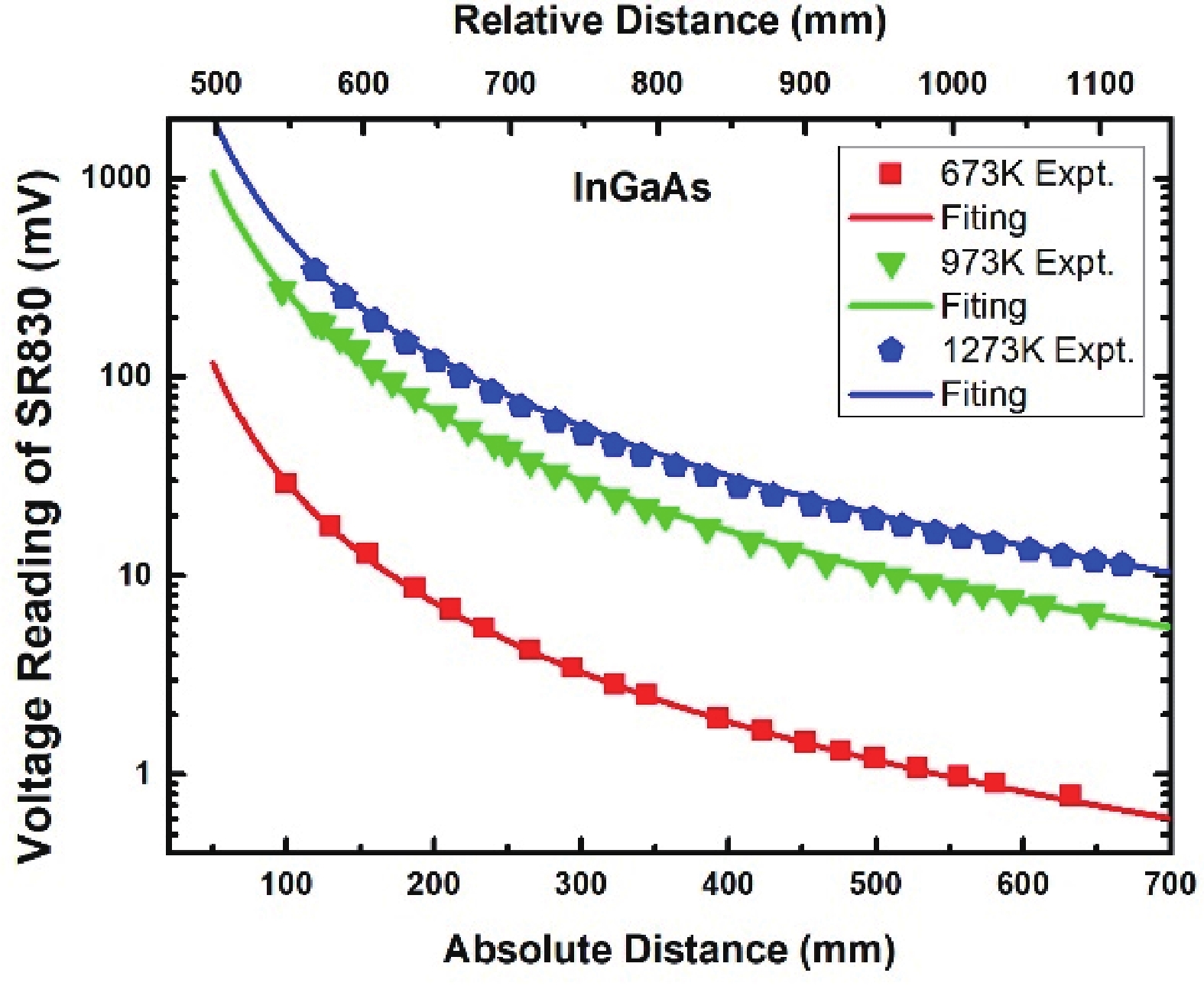
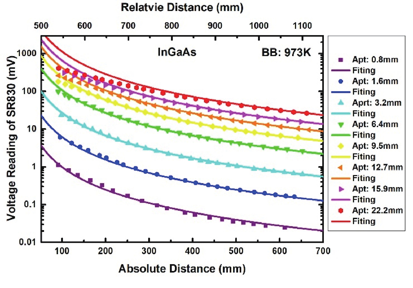
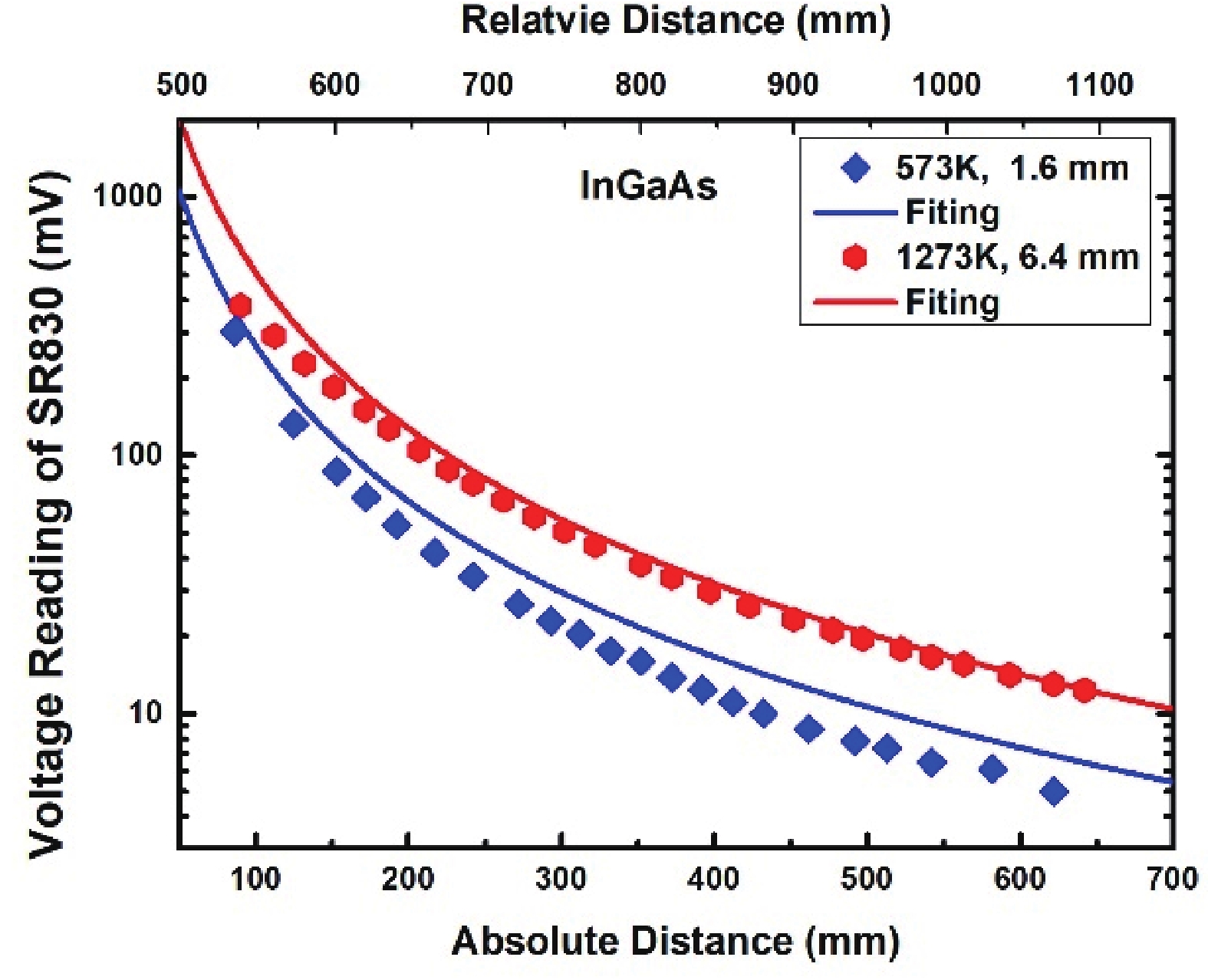
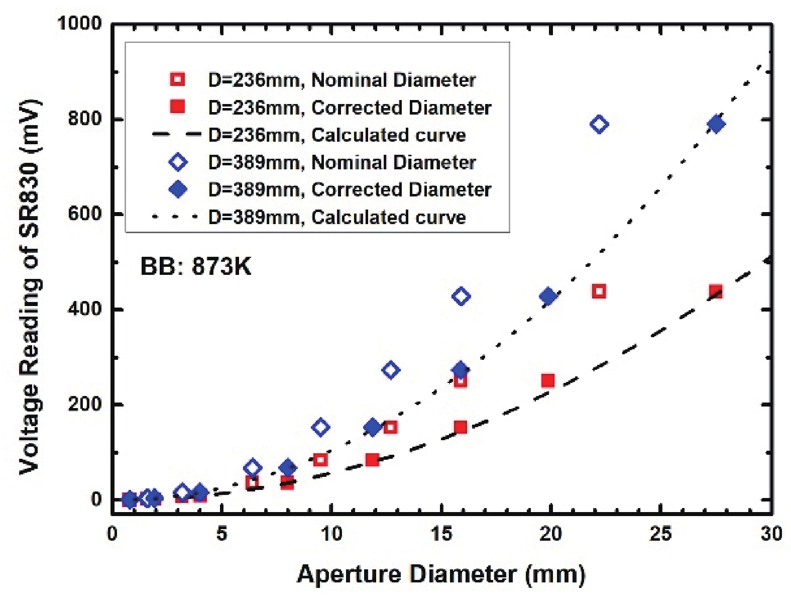
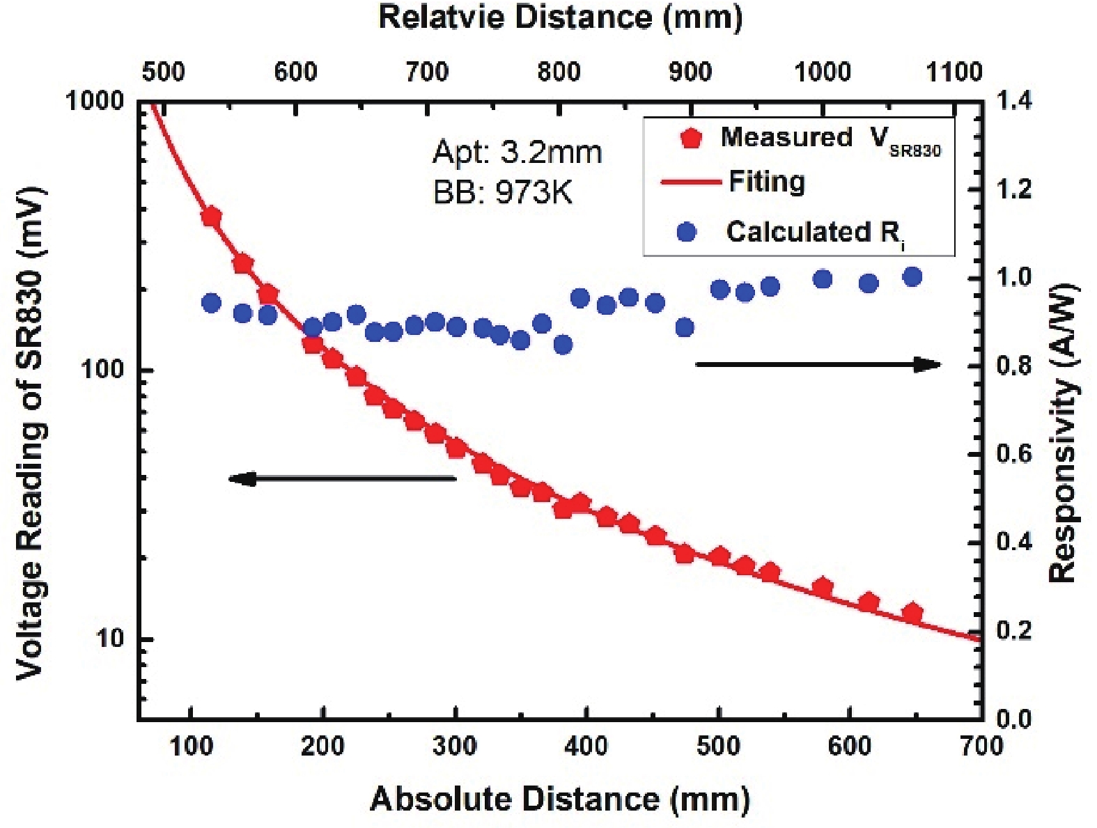
For the measurement of responsivity of an infrared photodetector, the most-used radiation source is a blackbody. In such a measurement system, distance between the blackbody, the photodetector and the aperture diameter are two parameters that contribute most measurement errors. In this work, we describe the configuration of our responsivity measurement system in great detail and present a method to calibrate the distance and aperture diameter. The core of this calibration method is to transfer direct measurements of these two parameters into an extraction procedure by fitting the experiment data to the calculated results. The calibration method is proved experimentally with a commercially extended InGaAs detector at a wide range of blackbody temperature, aperture diameter and distance. Then proof procedures are further extended into a detector fabricated in our laboratory and consistent results were obtained.
J. Semicond.
2023, 44(10): 102302 doi: 10.1088/1674-4926/44/10/102302

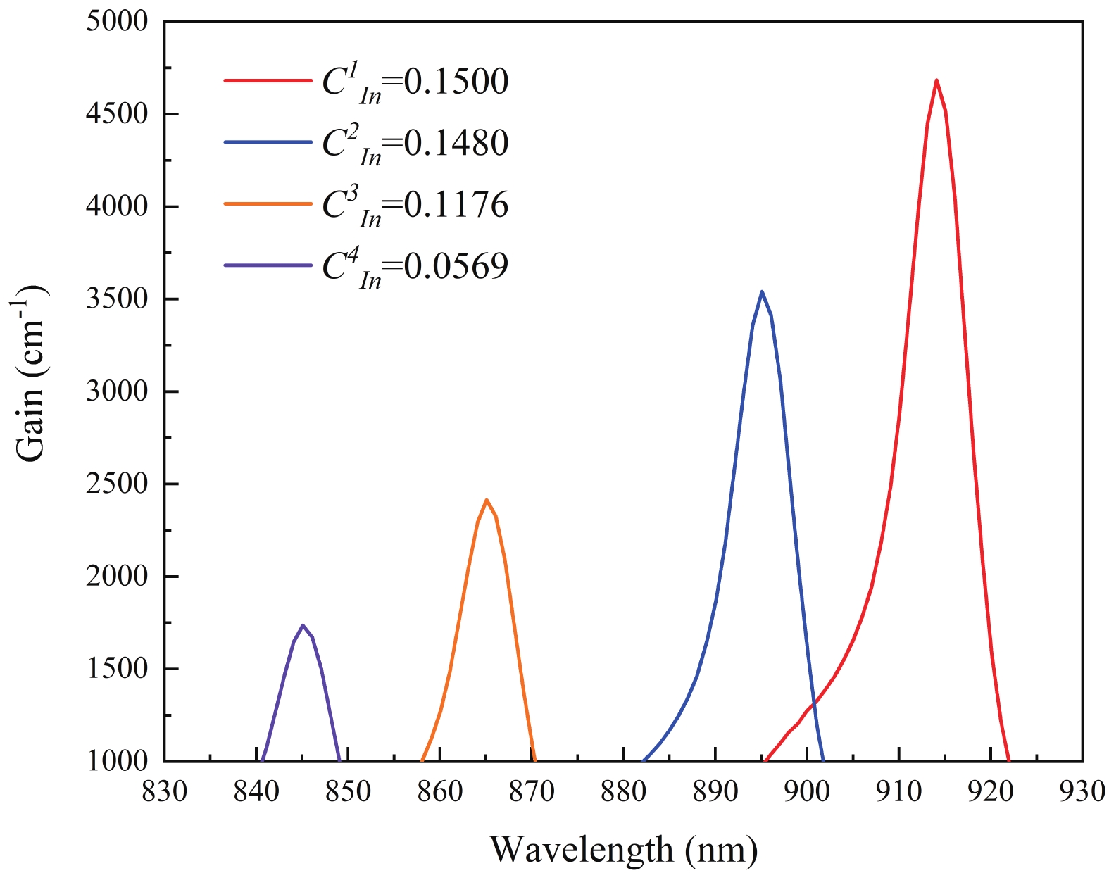
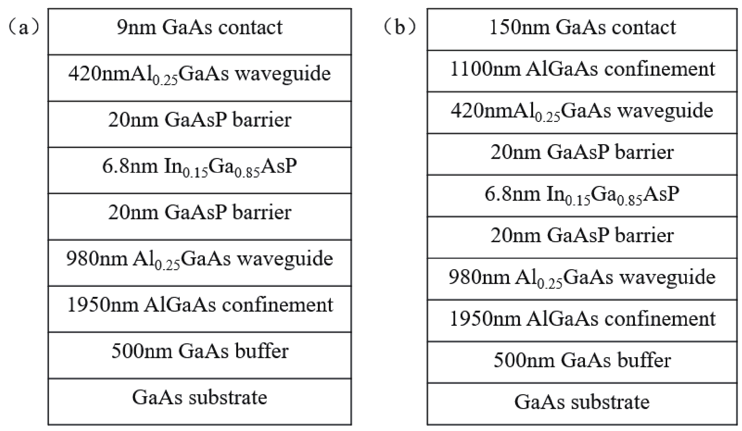
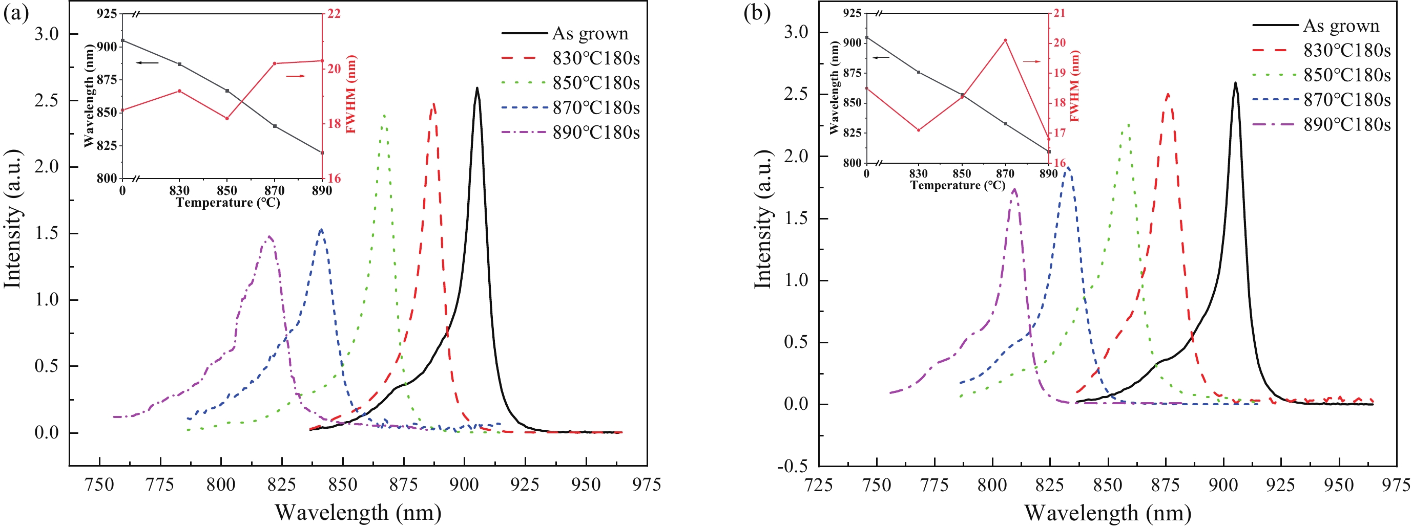
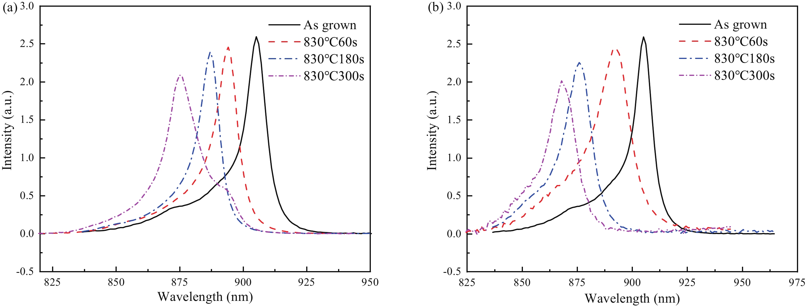
Output power and reliability are the most important characteristic parameters of semiconductor lasers. However, catastrophic optical damage (COD), which usually occurs on the cavity surface, will seriously damage the further improvement of the output power and affect the reliability. To improve the anti-optical disaster ability of the cavity surface, a non-absorption window (NAW) is adopted for the 915 nm InGaAsP/GaAsP single-quantum well semiconductor laser using quantum well mixing (QWI) induced by impurity-free vacancy. Both the principle and the process of point defect diffusion are described in detail in this paper. We also studied the effects of annealing temperature, annealing time, and the thickness of SiO2 film on the quantum well mixing in a semiconductor laser with a primary epitaxial structure, which is distinct from the previous structures. We found that when compared with the complete epitaxial structure, the blue shift of the semiconductor laser with the primary epitaxial structure is larger under the same conditions. To obtain the appropriate blue shift window, the primary epitaxial structure can use a lower annealing temperature and shorter annealing time. In addition, the process is less expensive. We also provide references for upcoming device fabrication.


J. Semicond.
2023, 44(10): 102401 doi: 10.1088/1674-4926/44/10/102401
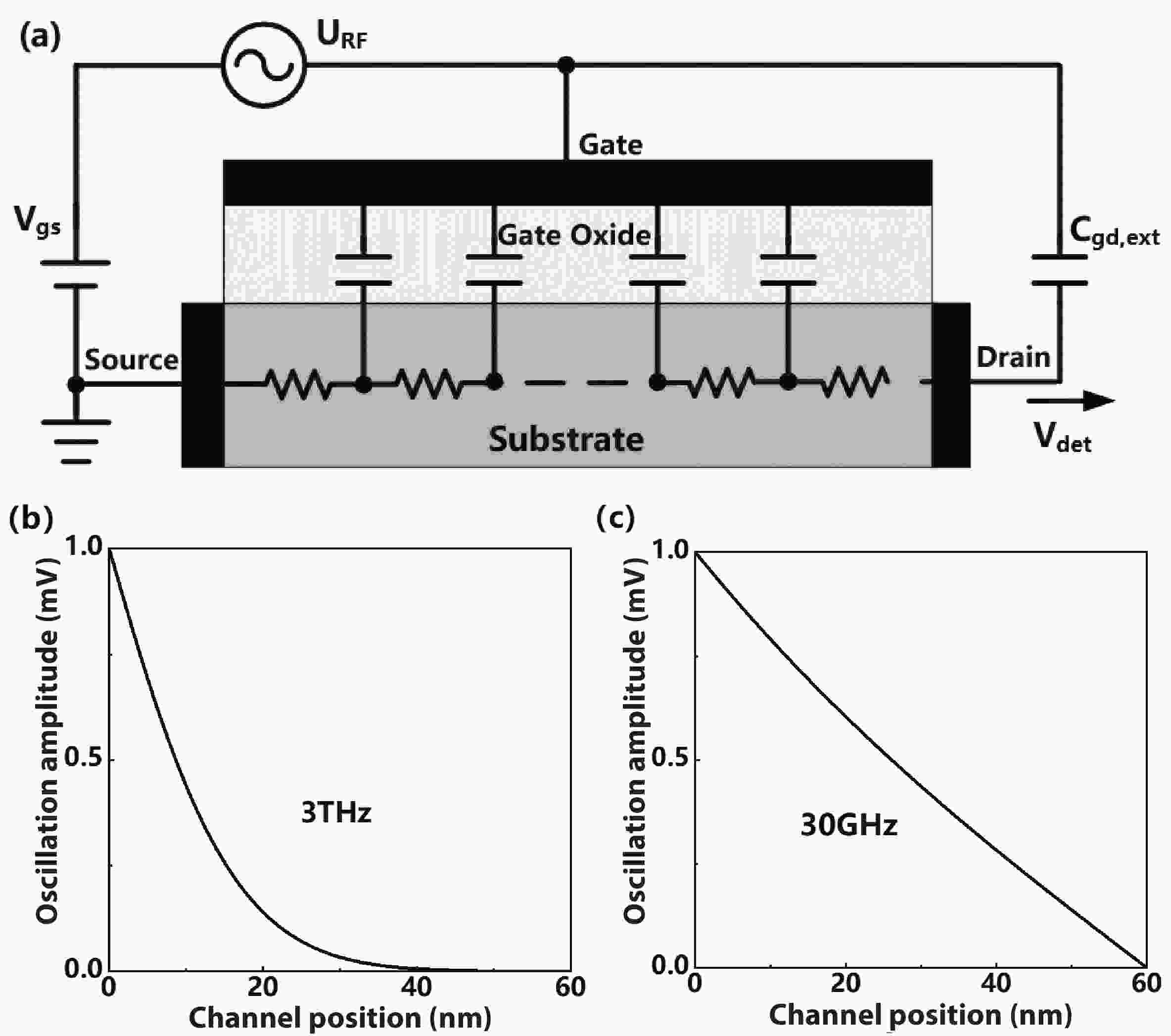
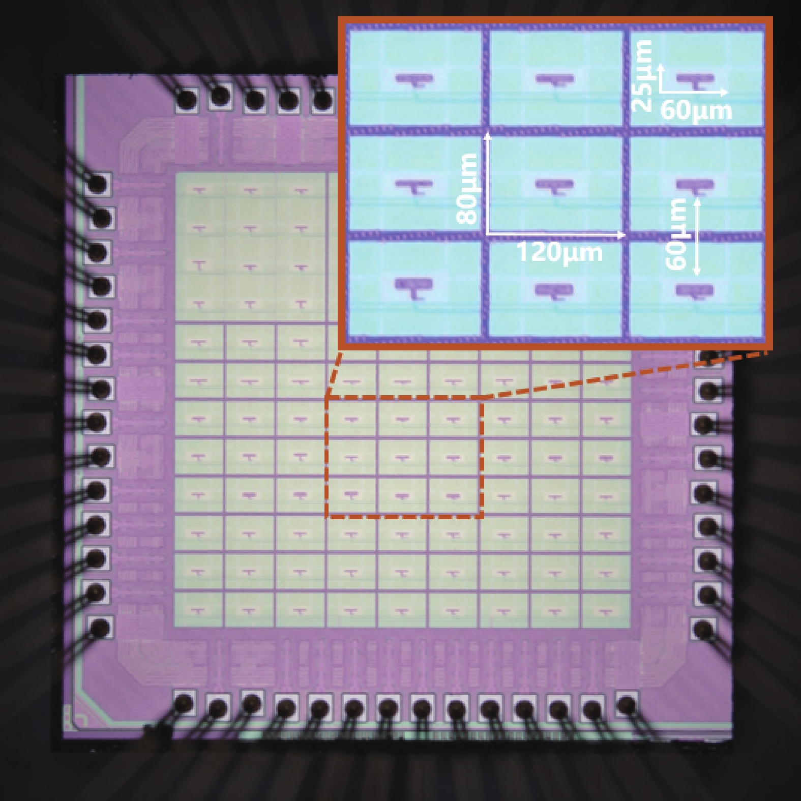
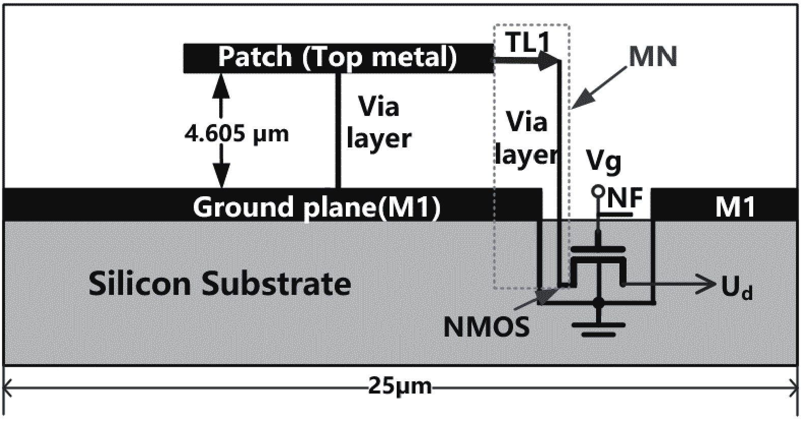
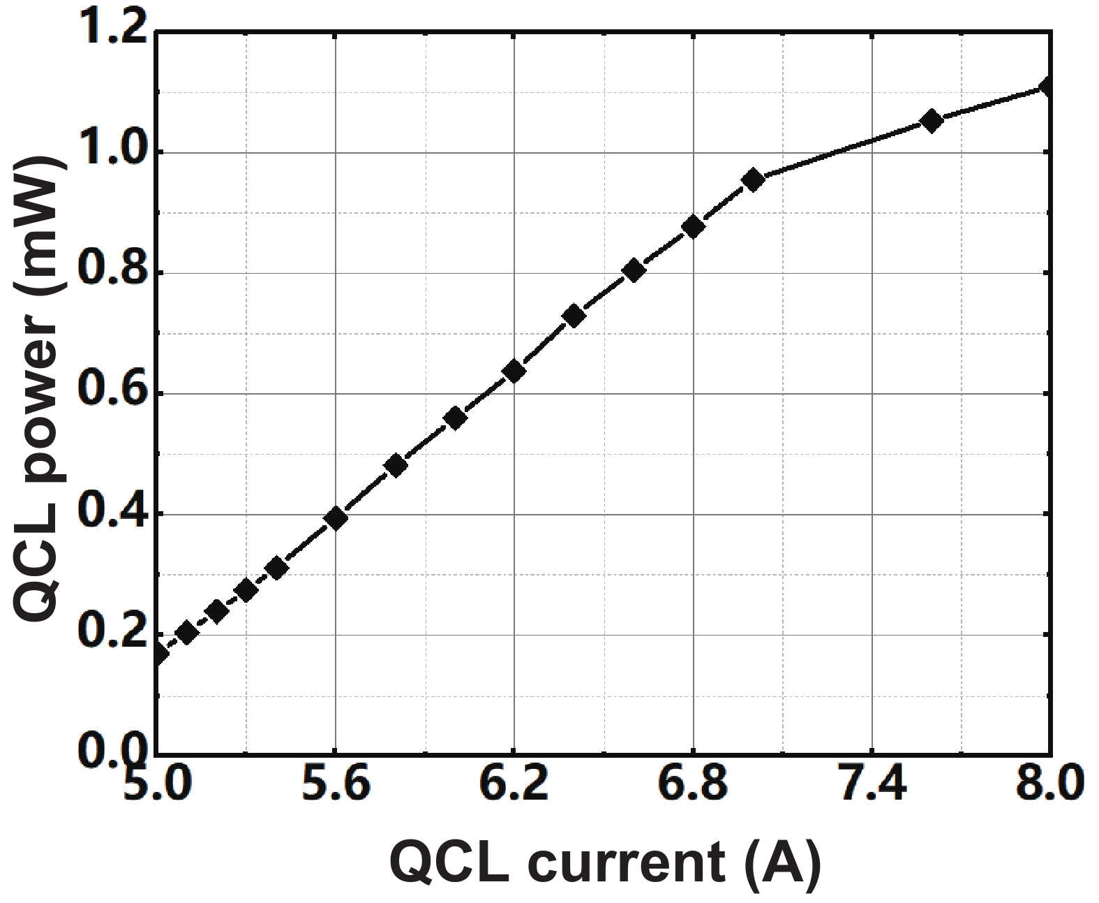
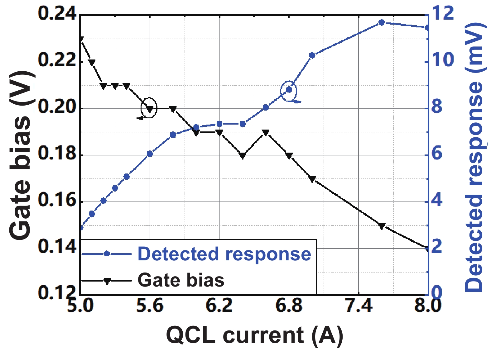
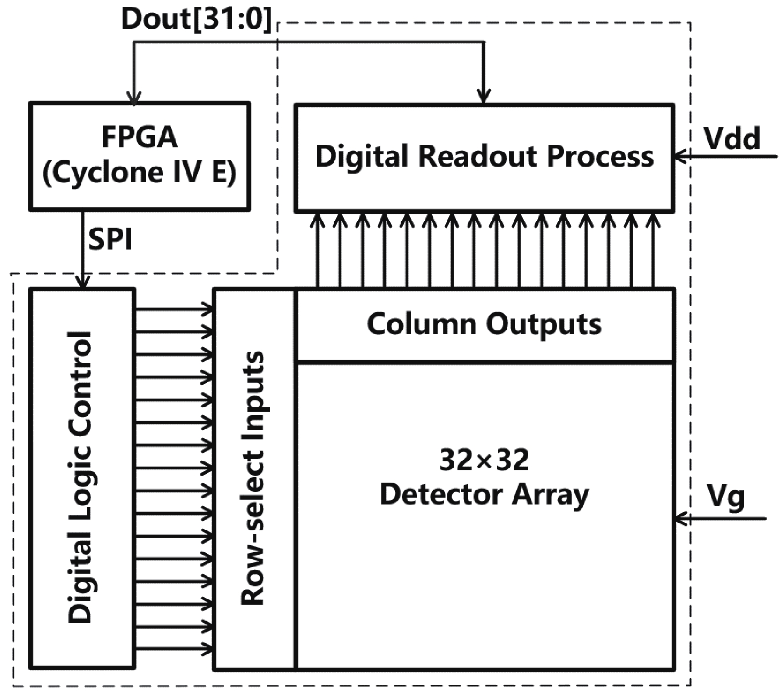
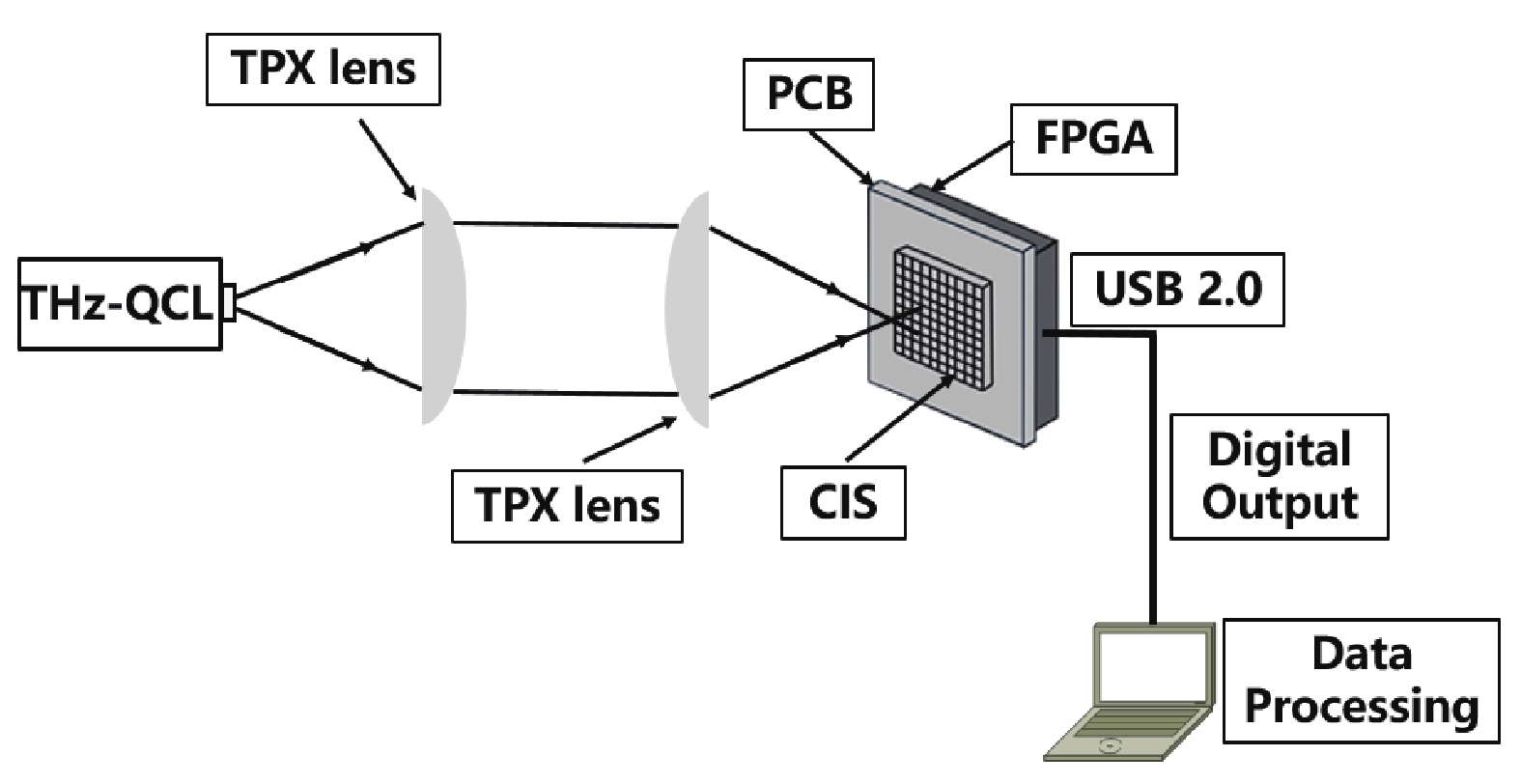
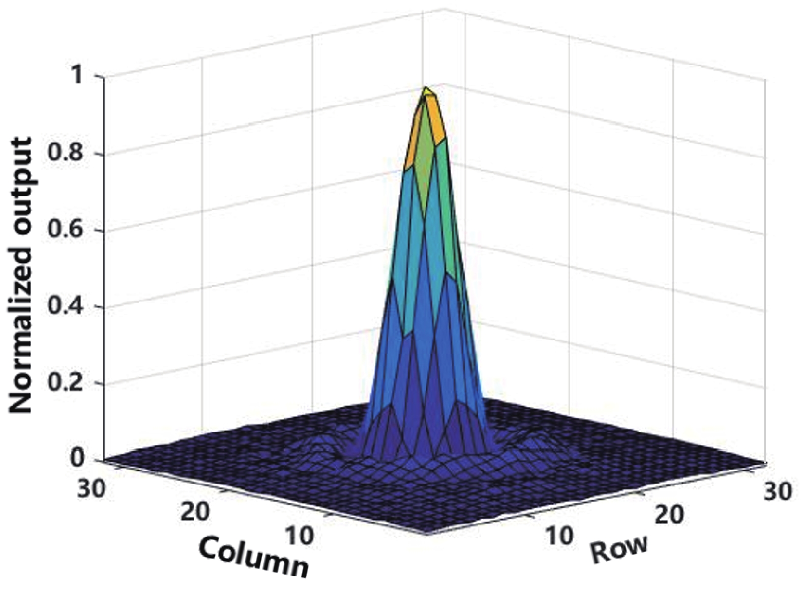
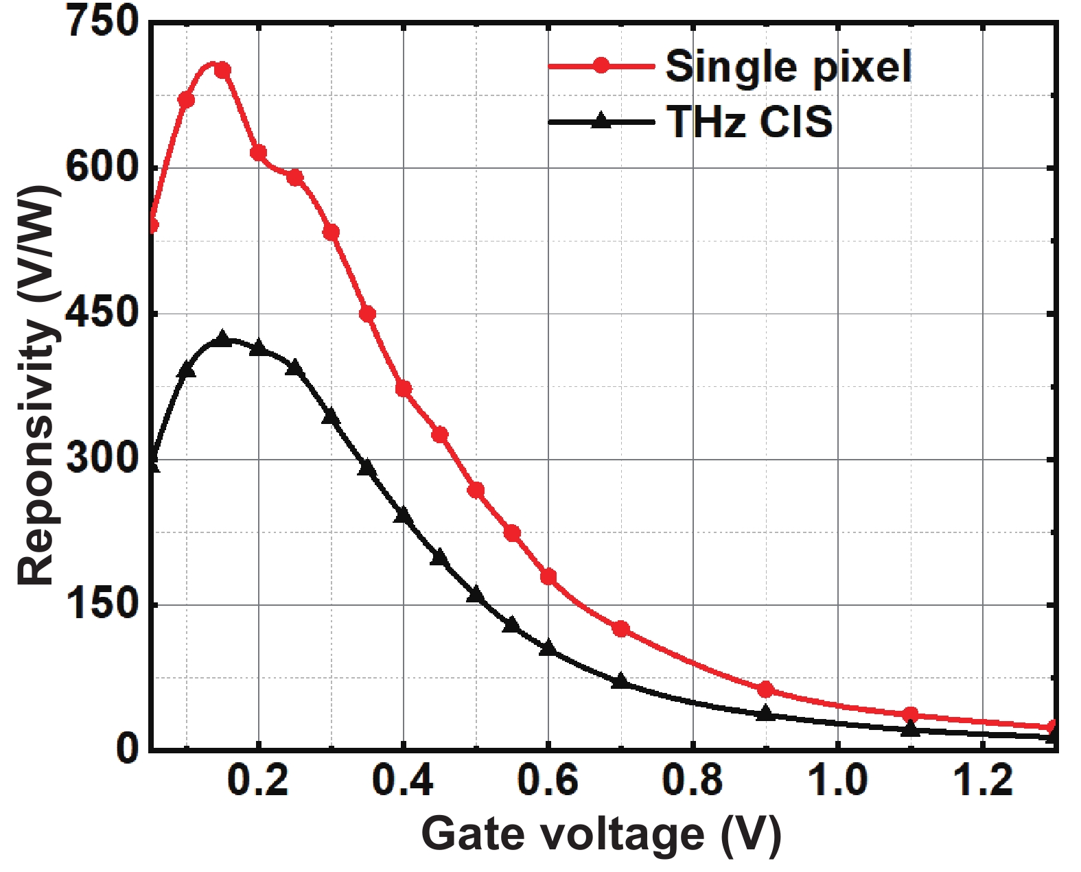
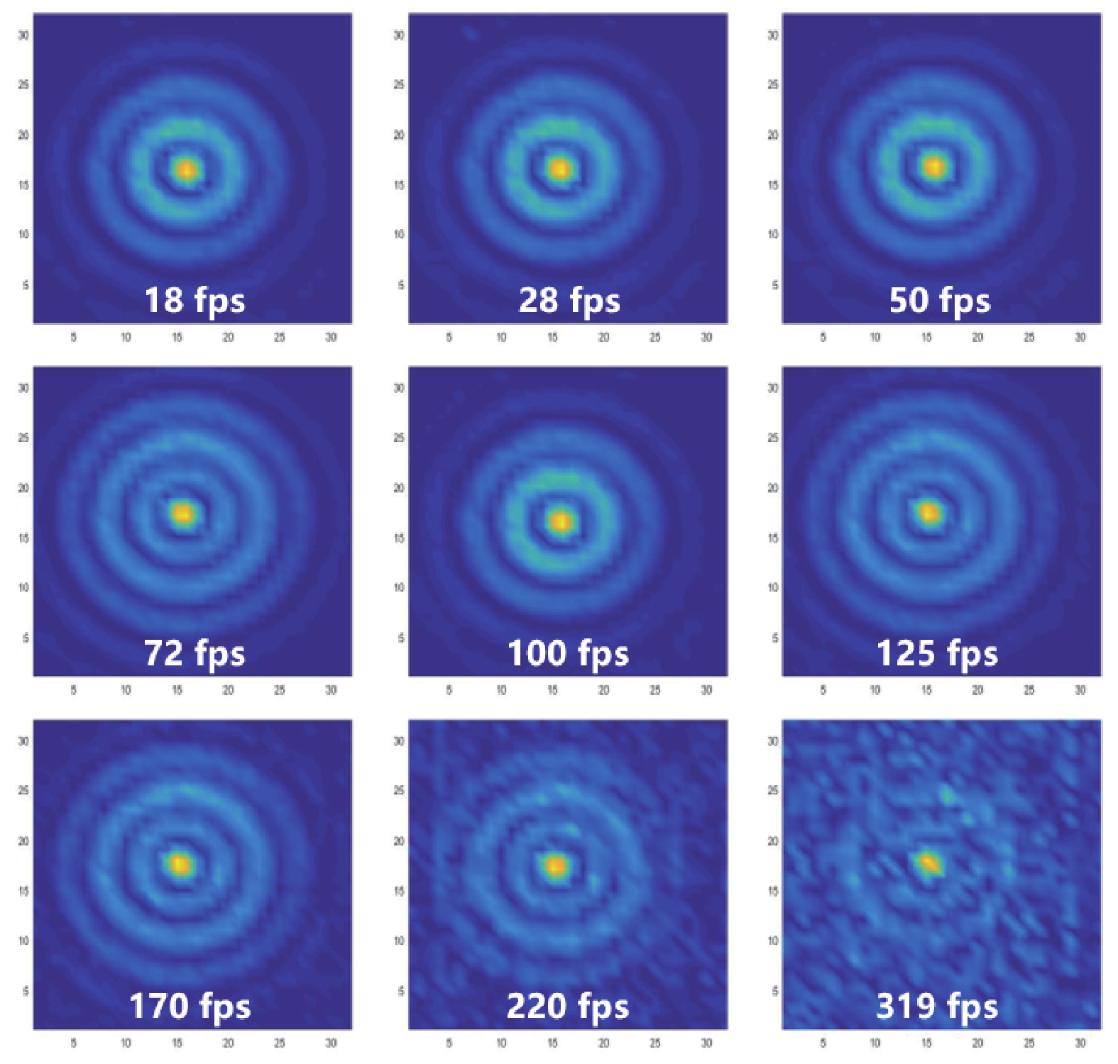
This paper describes a promising route for the exploration and development of 3.0 THz sensing and imaging with FET-based power detectors in a standard 65 nm CMOS process. Based on the plasma-wave theory proposed by Dyakonov and Shur, we designed high-responsivity and low-noise multiple detectors for monitoring a pulse-mode 3.0 THz quantum cascade laser (QCL). Furthermore, we present a fully integrated high-speed 32 × 32-pixel 3.0 THz CMOS image sensor (CIS). The full CIS measures 2.81 × 5.39 mm2 and achieves a 423 V/W responsivity (Rv) and a 5.3 nW integral noise equivalent power (NEP) at room temperature. In experiments, we demonstrate a testing speed reaching 319 fps under continuous-wave (CW) illumination of a 3.0 THz QCL. The results indicate that our terahertz CIS has excellent potential in cost-effective and commercial THz imaging and material detection.


J. Semicond.
2023, 44(10): 102402 doi: 10.1088/1674-4926/44/10/102402
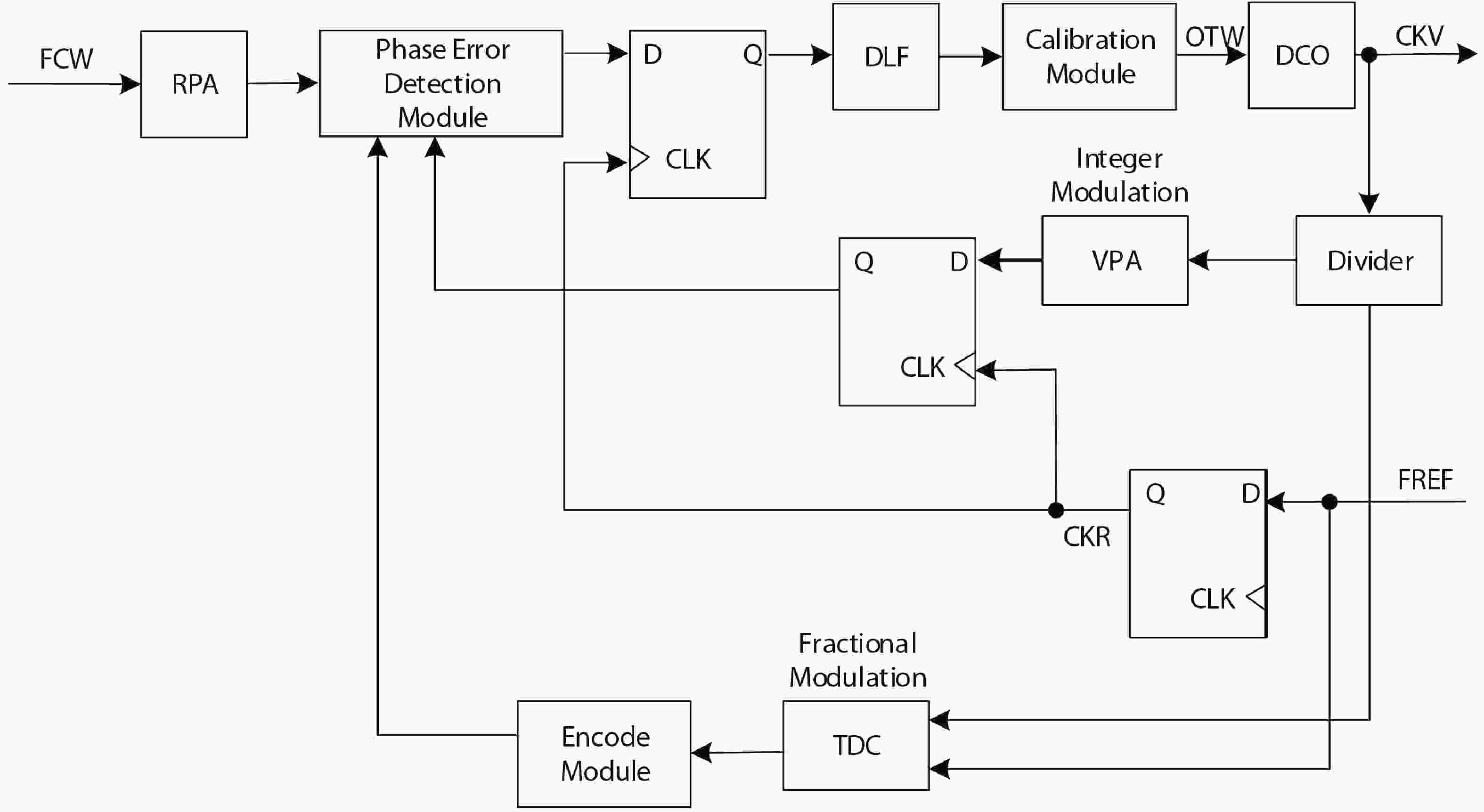
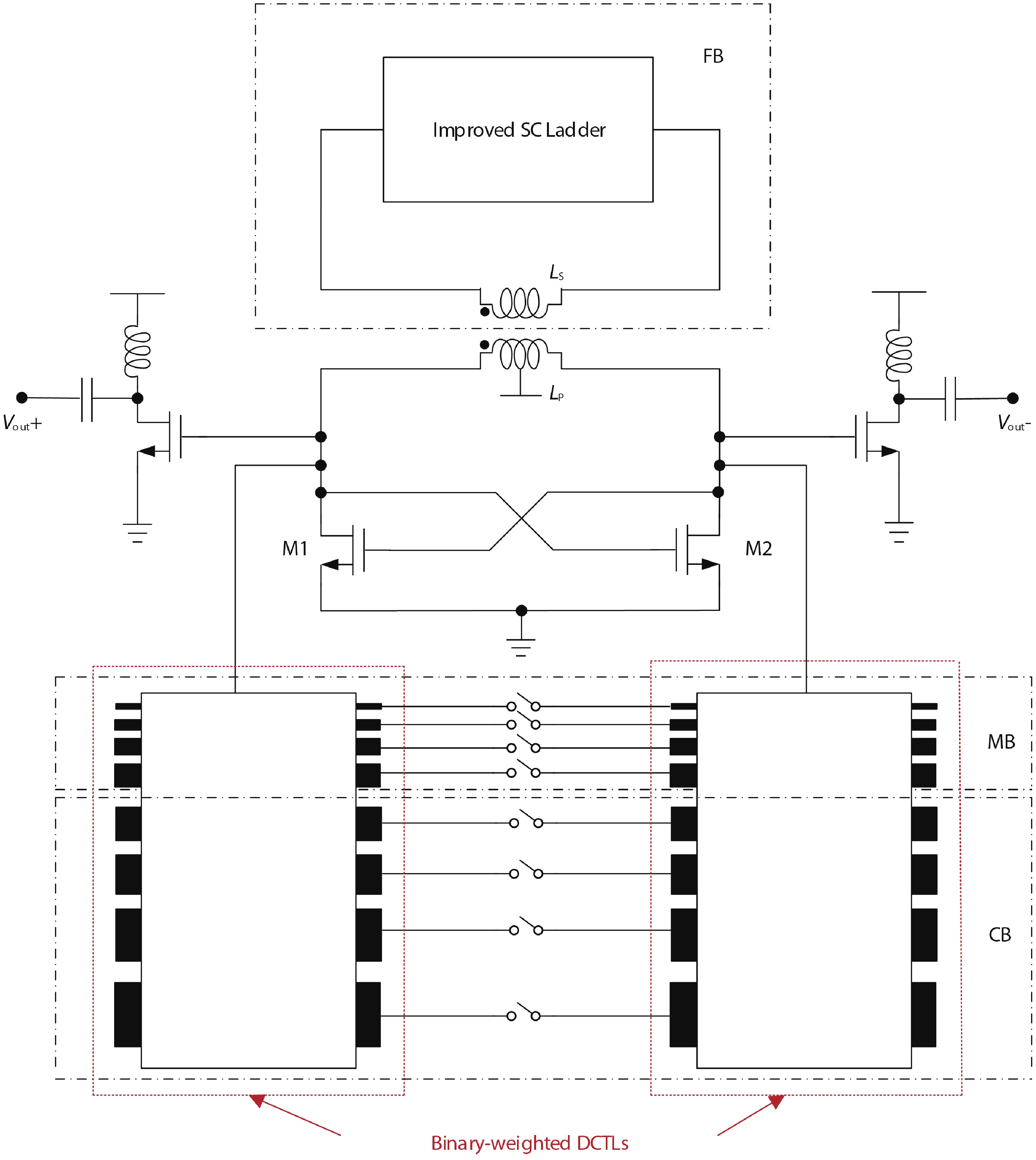
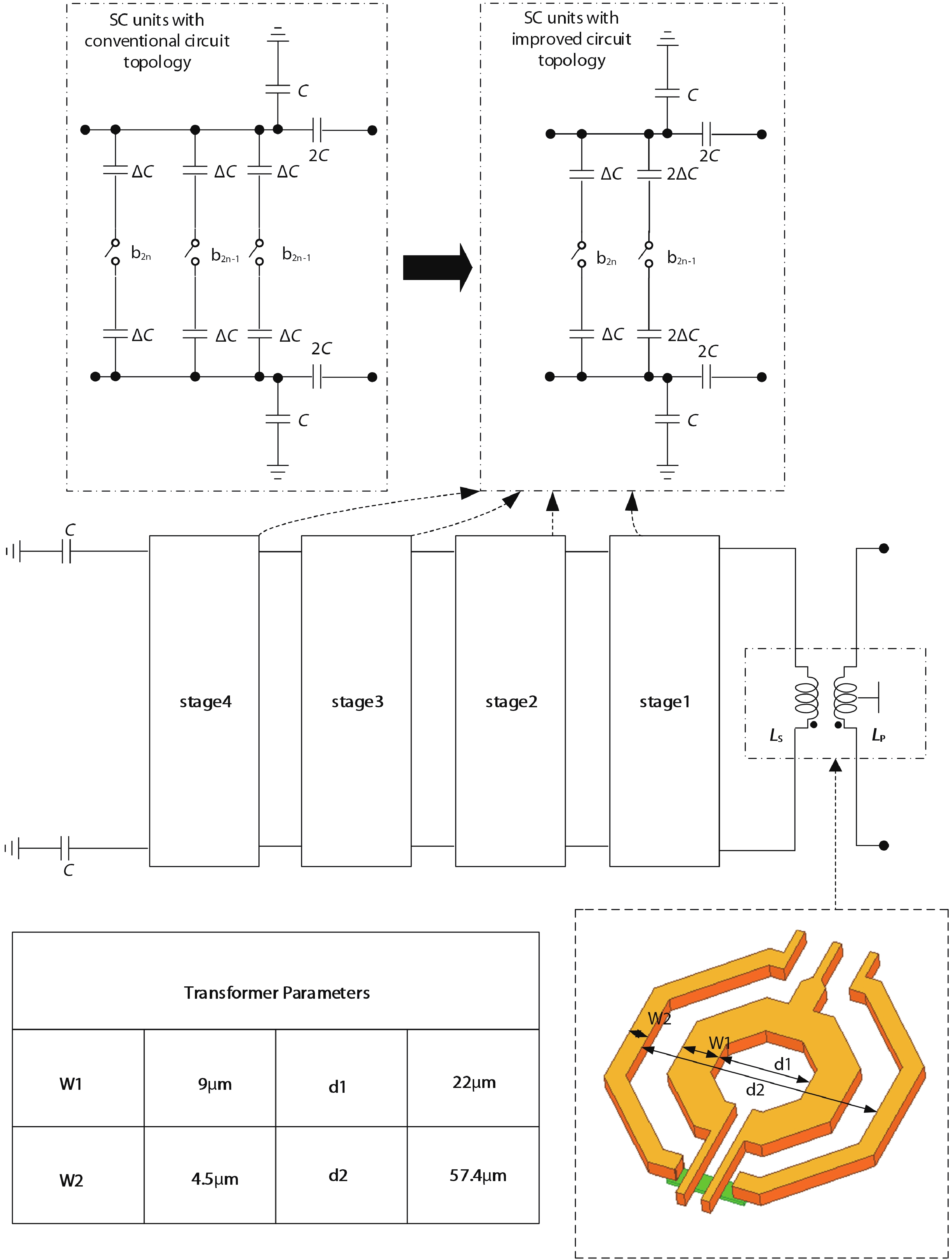
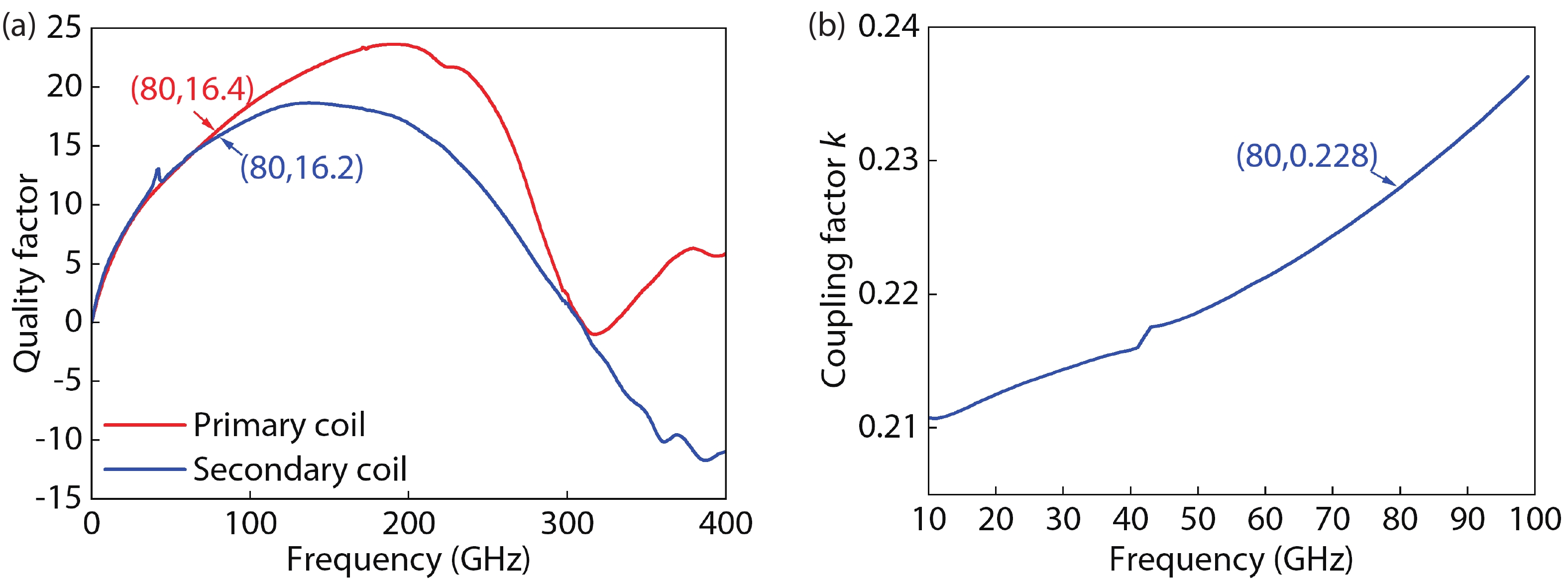
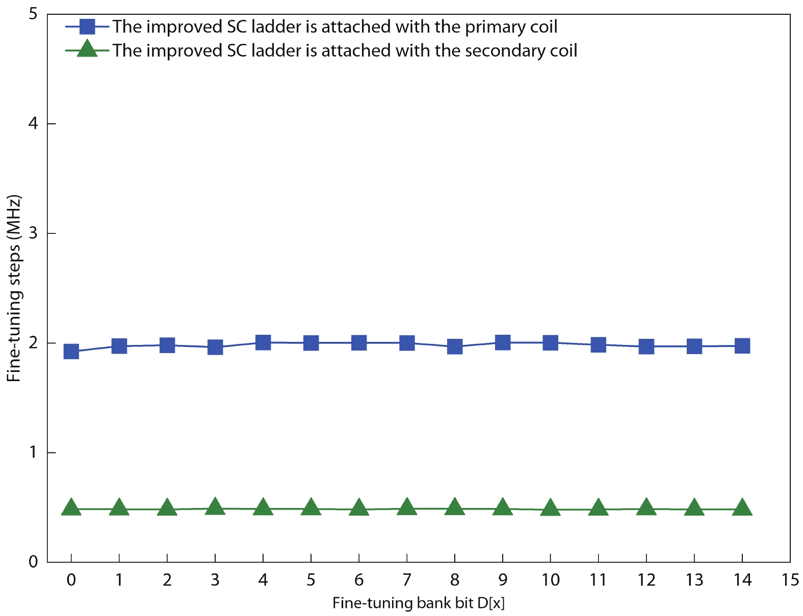
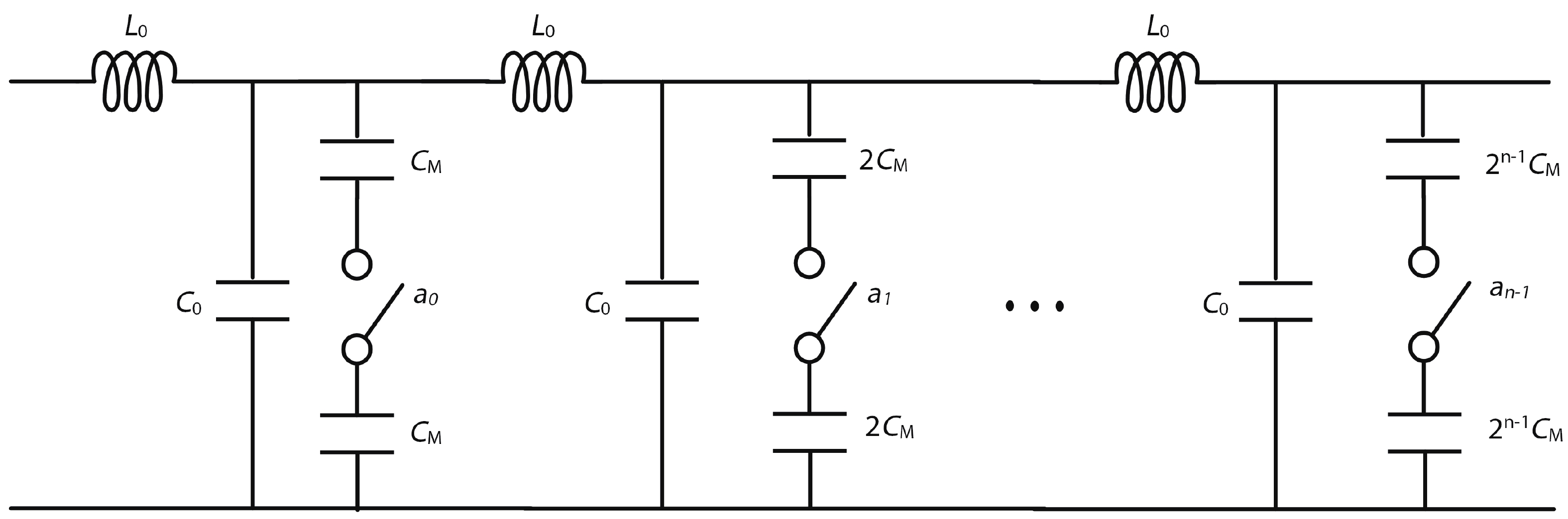
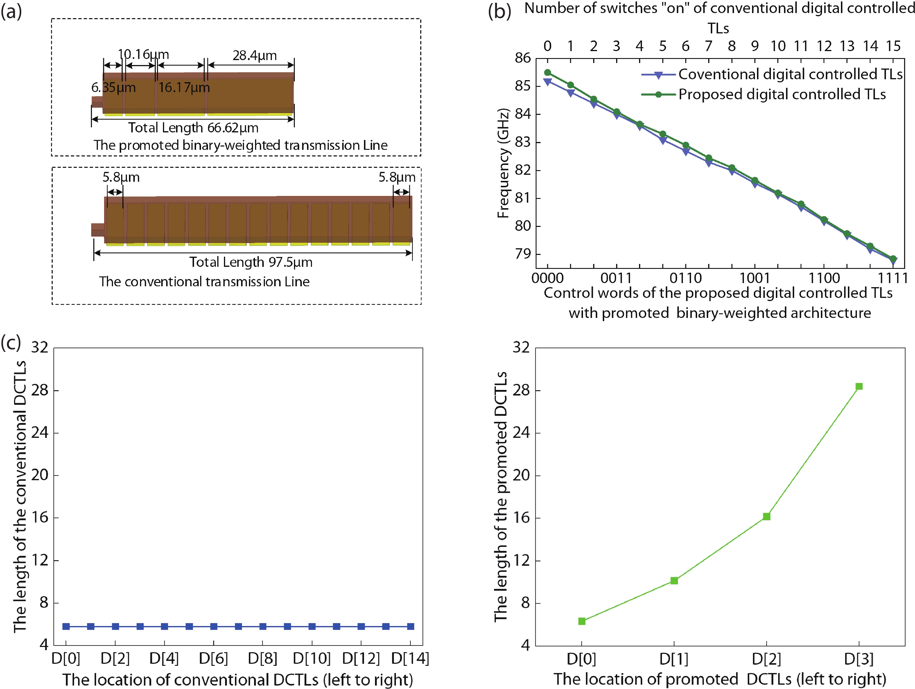
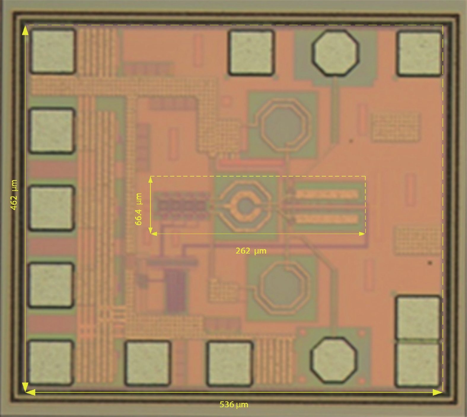
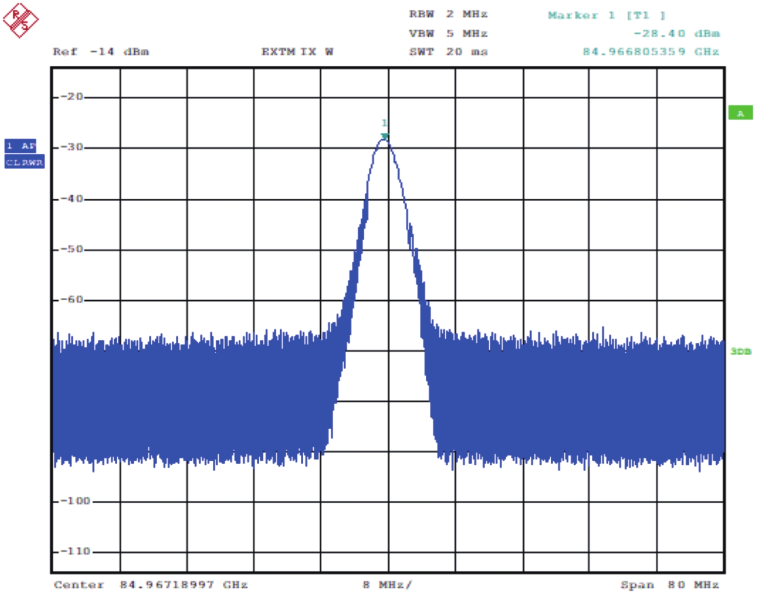
An 80-GHz DCO based on modified hybrid tuning banks is introduced in this paper. To achieve sub-MHz frequency resolution with reduced circuit complexity, the improved circuit topology replaces the conventional circuit topology with two binary-weighted SC cells, enabling eight SC-cell-based improved SC ladders to achieve the same fine-tuning steps as twelve SC-cell-based conventional SC ladders. To achieve lower phase noise and smaller chip size, the promoted binary-weighted digitally controlled transmission lines (DCTLs) are used to implement the coarse and medium tuning banks of the DCO. Compared to the conventional thermometer-coded DCTLs, control bits of the proposed DCTLs are reduced from 30 to 8, and the total length is reduced by 34.3% (from 122.76 to 80.66 μm). Fabricated in 40-nm CMOS, the DCO demonstrated in this work features a small fine-tuning step (483 kHz), a high oscillation frequency (79–85 GHz), and a smaller chip size (0.017 mm2). Compared to previous work, the modified DCO exhibits an excellent figure of merit with an area (FoMA) of –198 dBc/Hz.


J. Semicond.
2023, 44(10): 102801 doi: 10.1088/1674-4926/44/10/102801

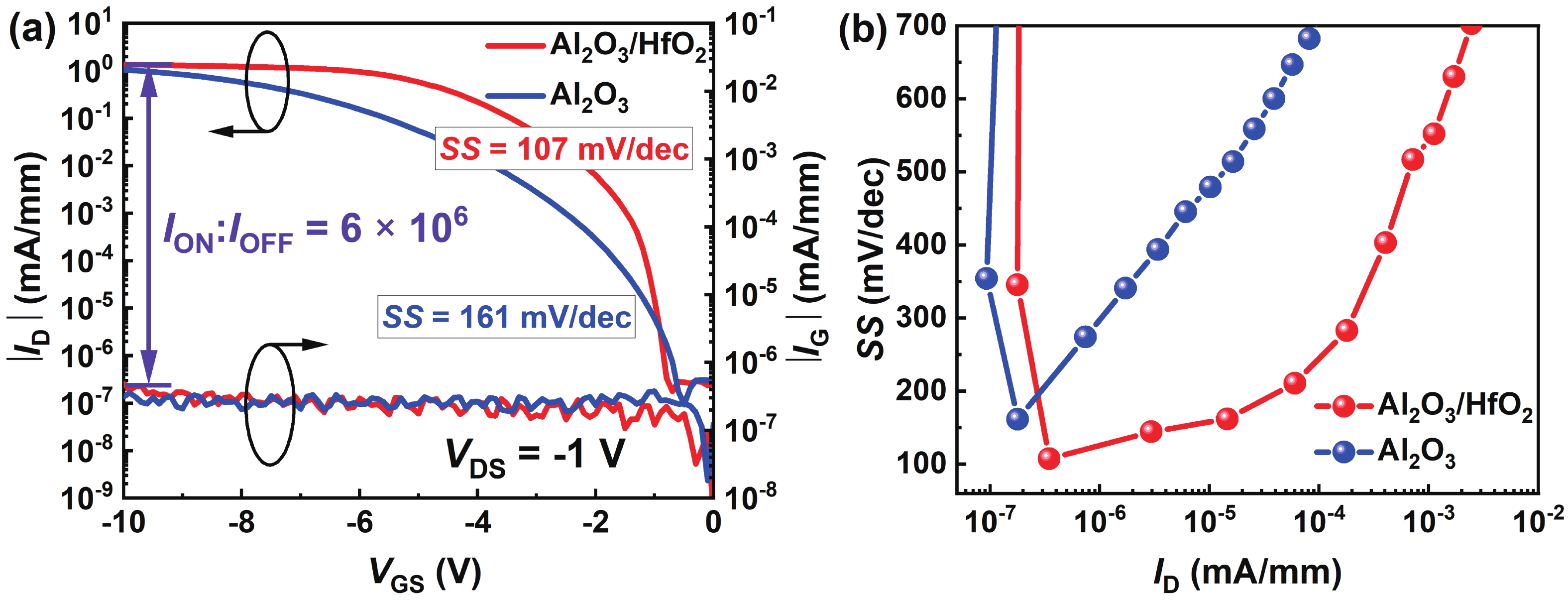
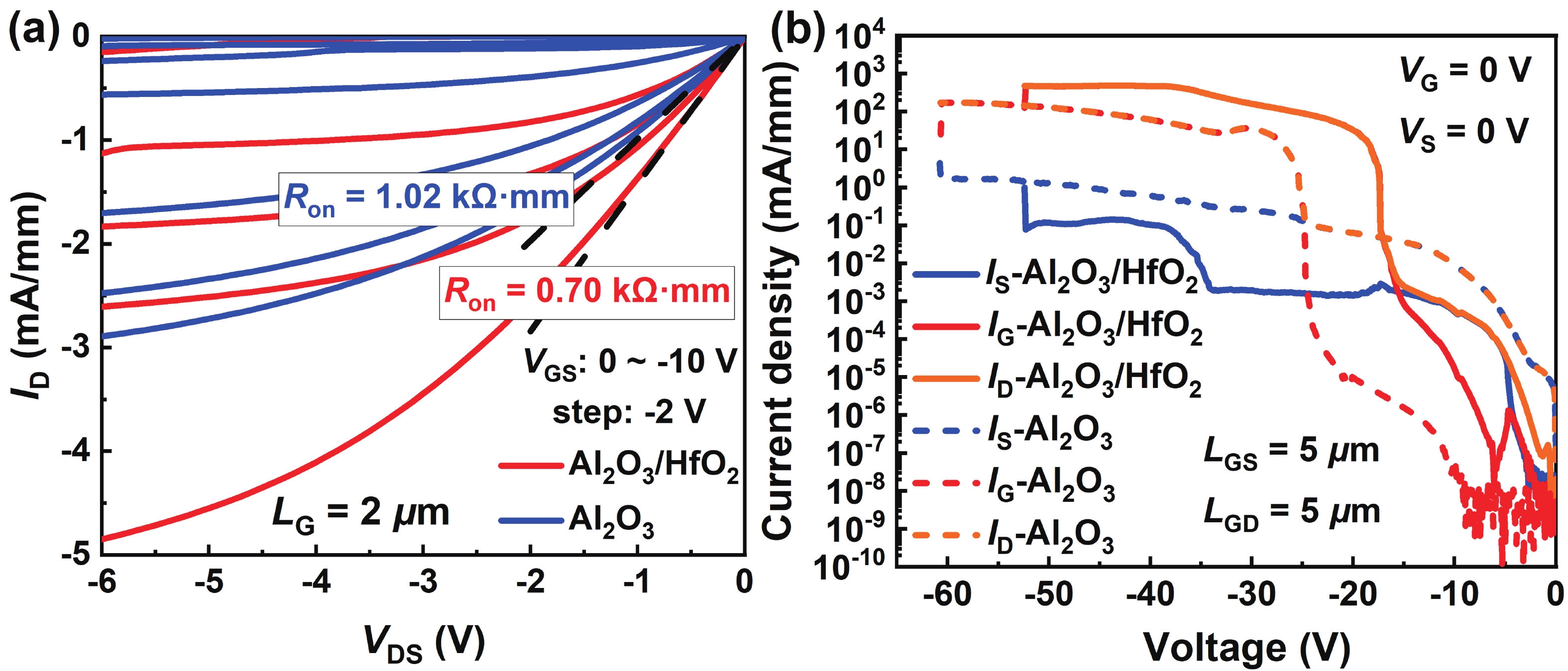
In this letter, an enhancement-mode (E-mode) GaN p-channel field-effect transistor (p-FET) with a high current density of −4.9 mA/mm based on a O3-Al2O3/HfO2 (5/15 nm) stacked gate dielectric was demonstrated on a p++-GaN/p-GaN/AlN/AlGaN/AlN/GaN/Si heterostructure. Attributed to the p++-GaN capping layer, a good linear ohmic I−V characteristic featuring a low-contact resistivity (ρc) of 1.34 × 10⁻⁴ Ω·cm2 was obtained. High gate leakage associated with the HfO2 high-k gate dielectric was effectively blocked by the 5-nm O3-Al2O3 insertion layer grown by atomic layer deposition, contributing to a high ION/IOFF ratio of 6 × 10⁶ and a remarkably reduced subthreshold swing (SS) in the fabricated p-FETs. The proposed structure is compelling for energy-efficient GaN complementary logic (CL) circuits.


J. Semicond.
2023, 44(10): 104101 doi: 10.1088/1674-4926/44/10/104101

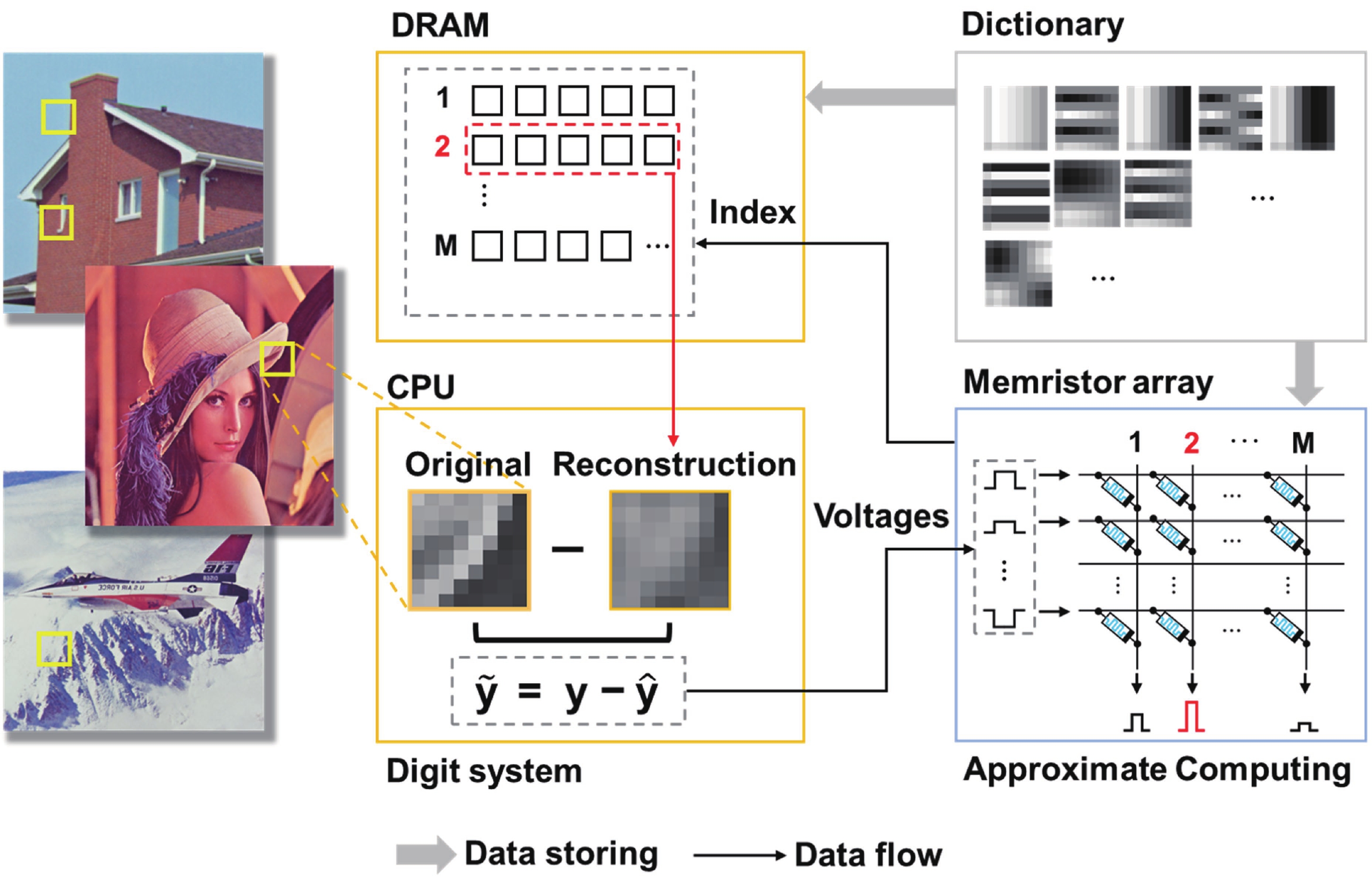
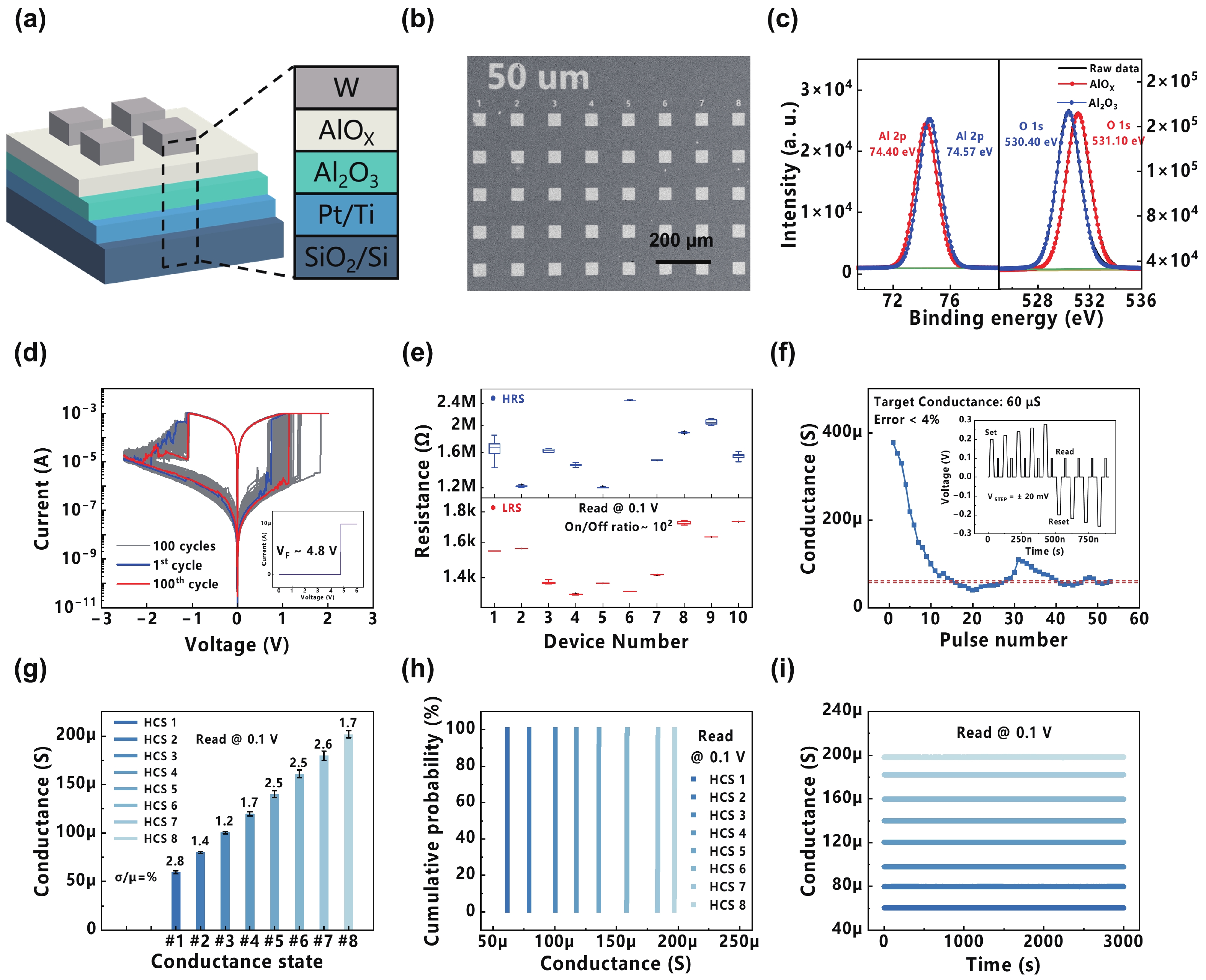
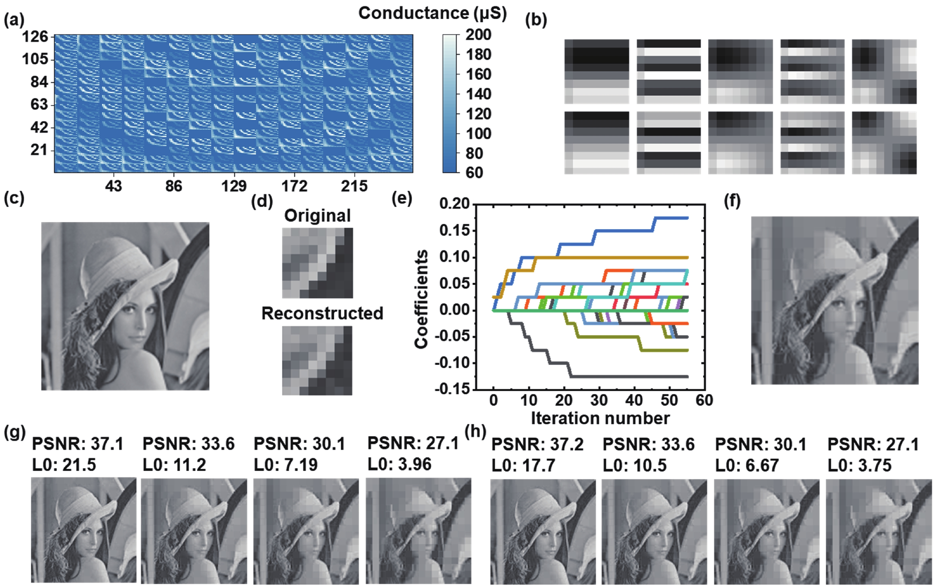
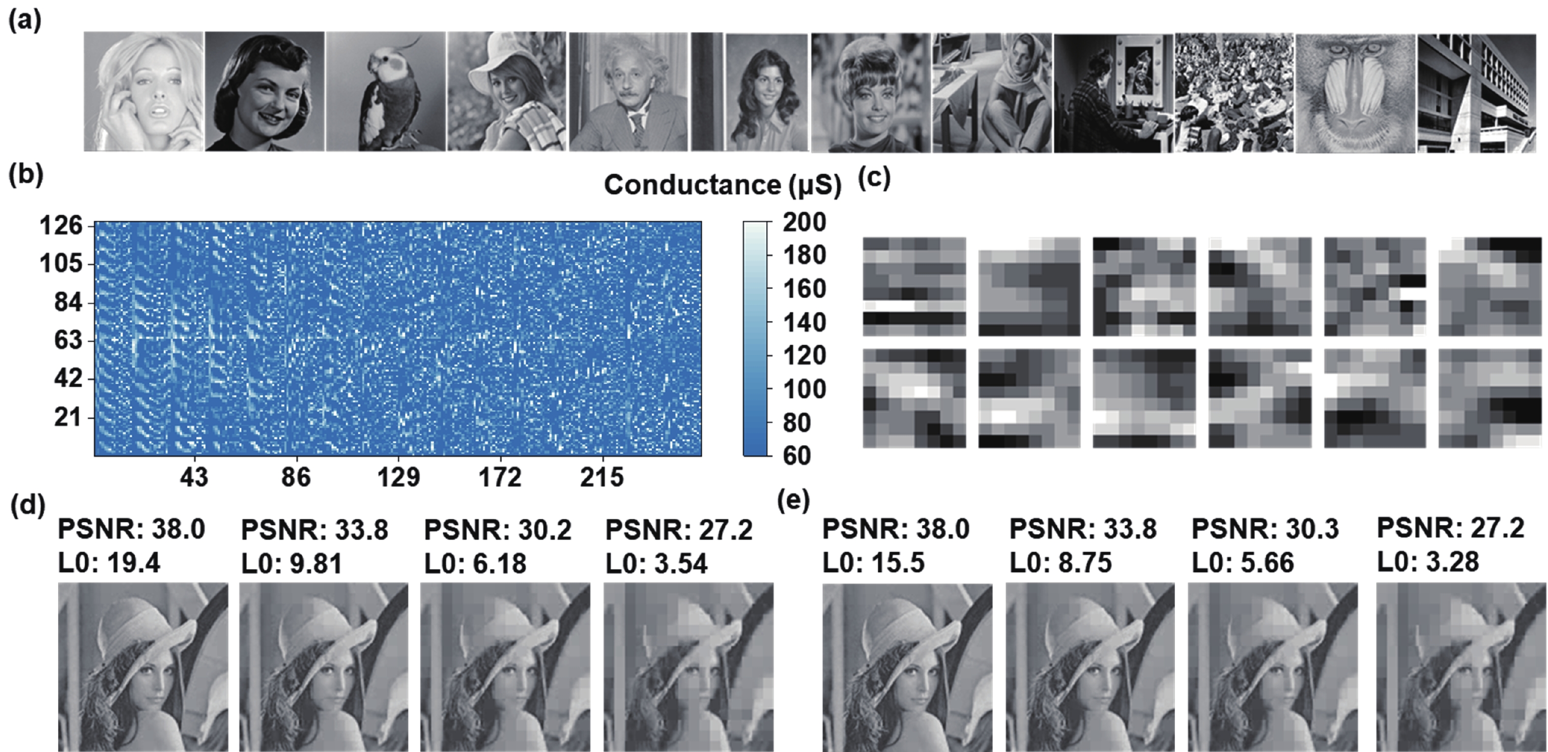
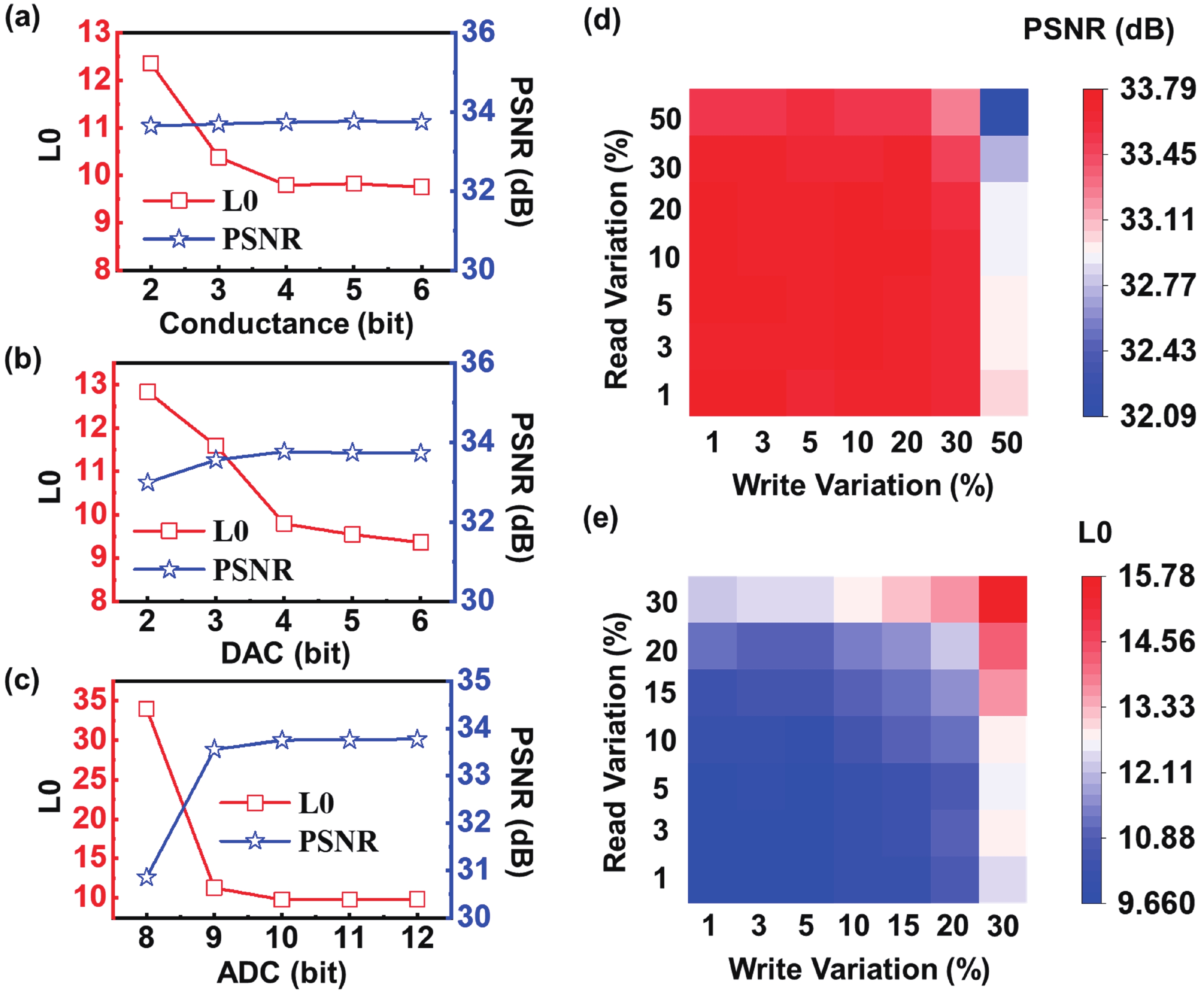
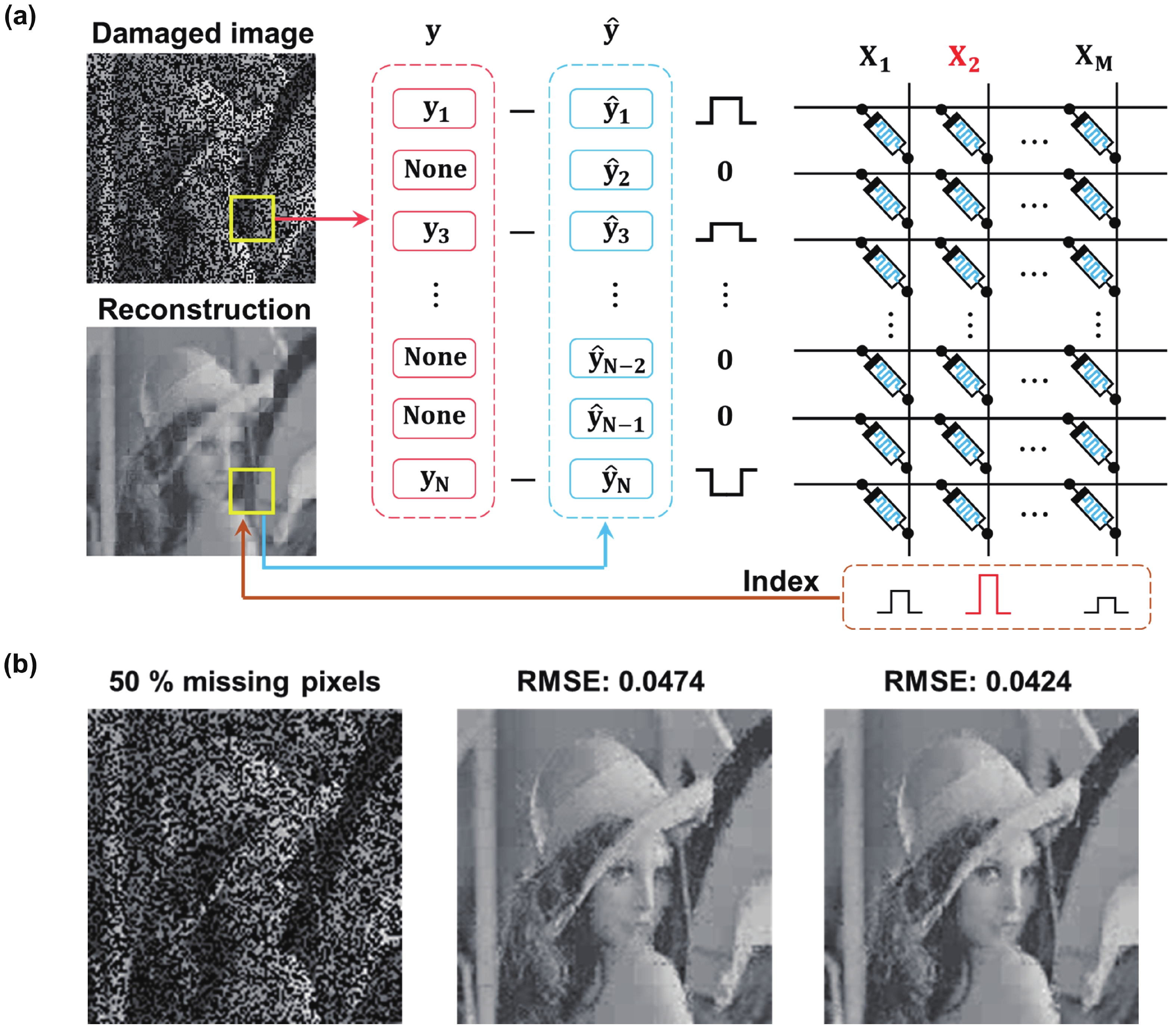
Sparse coding is a prevalent method for image inpainting and feature extraction, which can repair corrupted images or improve data processing efficiency, and has numerous applications in computer vision and signal processing. Recently, several memristor-based in-memory computing systems have been proposed to enhance the efficiency of sparse coding remarkably. However, the variations and low precision of the devices will deteriorate the dictionary, causing inevitable degradation in the accuracy and reliability of the application. In this work, a digital-analog hybrid memristive sparse coding system is proposed utilizing a multilevel Pt/Al2O3/AlOx/W memristor, which employs the forward stagewise regression algorithm: The approximate cosine distance calculation is conducted in the analog part to speed up the computation, followed by high-precision coefficient updates performed in the digital portion. We determine that four states of the aforementioned memristor are sufficient for the processing of natural images. Furthermore, through dynamic adjustment of the mapping ratio, the precision requirement for the digit-to-analog converters can be reduced to 4 bits. Compared to the previous system, our system achieves higher image reconstruction quality of the 38 dB peak-signal-to-noise ratio. Moreover, in the context of image inpainting, images containing 50% missing pixels can be restored with a reconstruction error of 0.0424 root-mean-squared error.