Issue Browser
Volume 45, Issue 1,
Jan 2024
Column
J. Semicond.
2024, 45(1): 011501 doi: 10.1088/1674-4926/45/1/011501

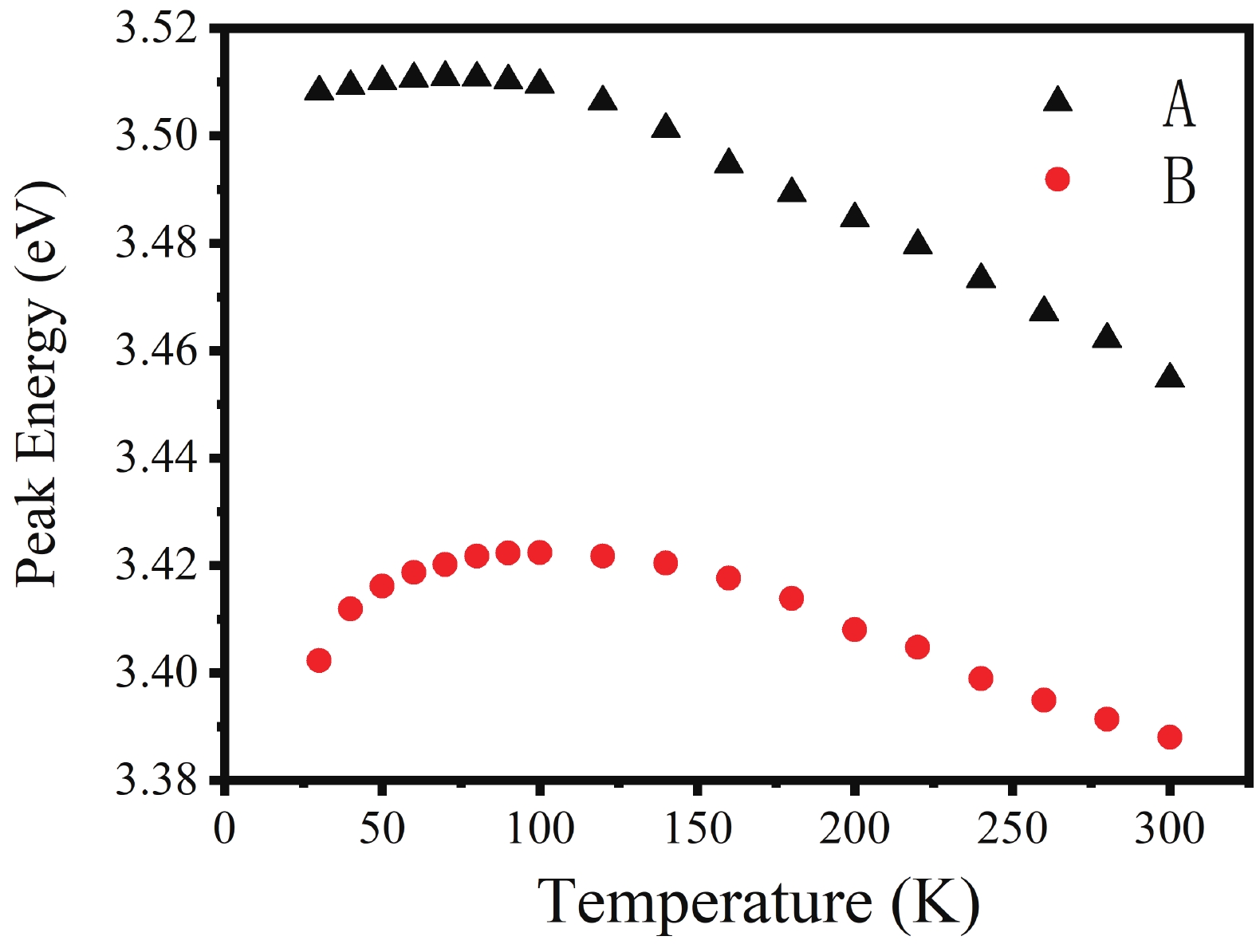
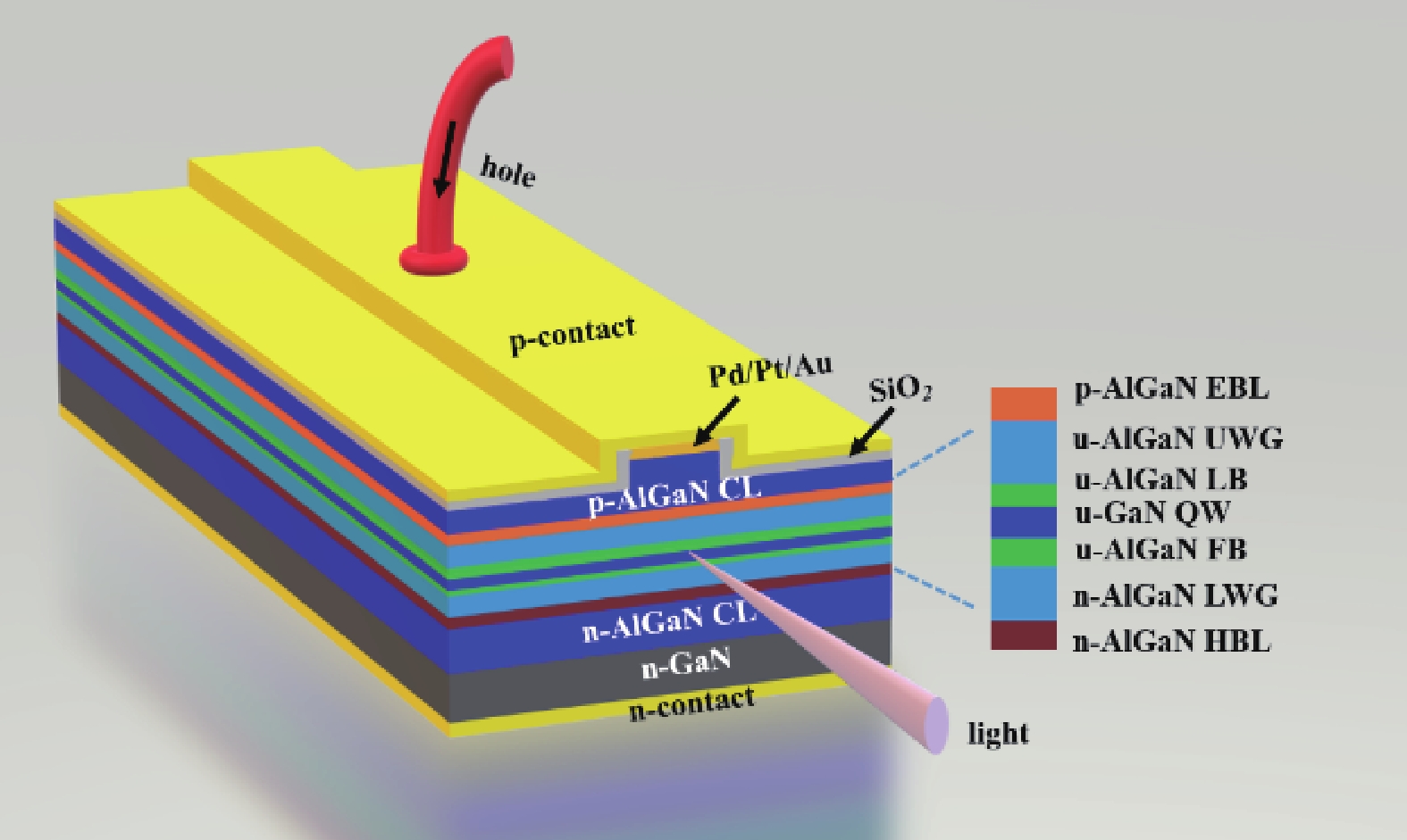
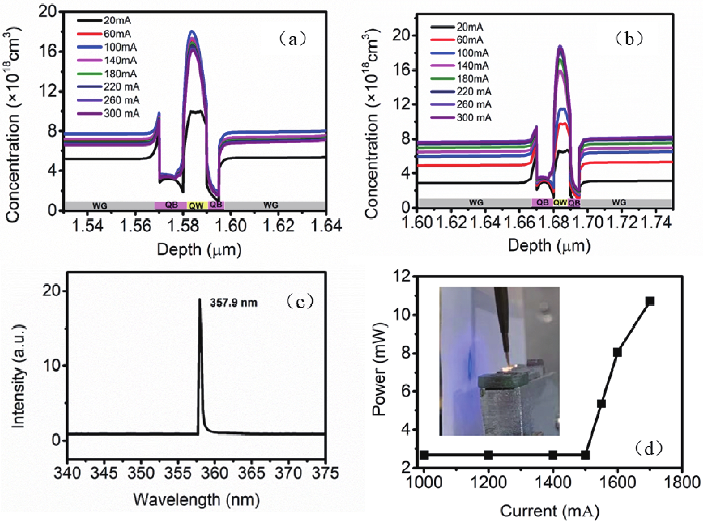
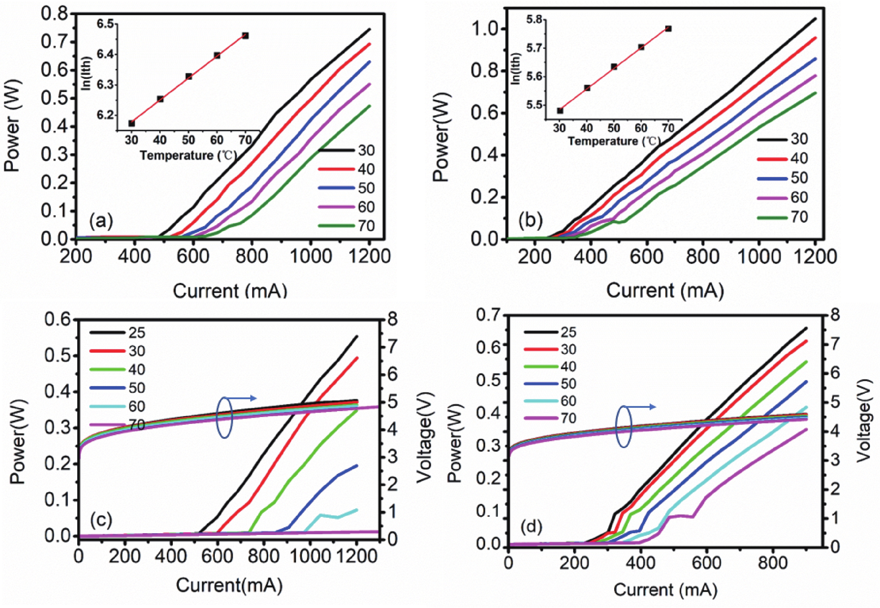
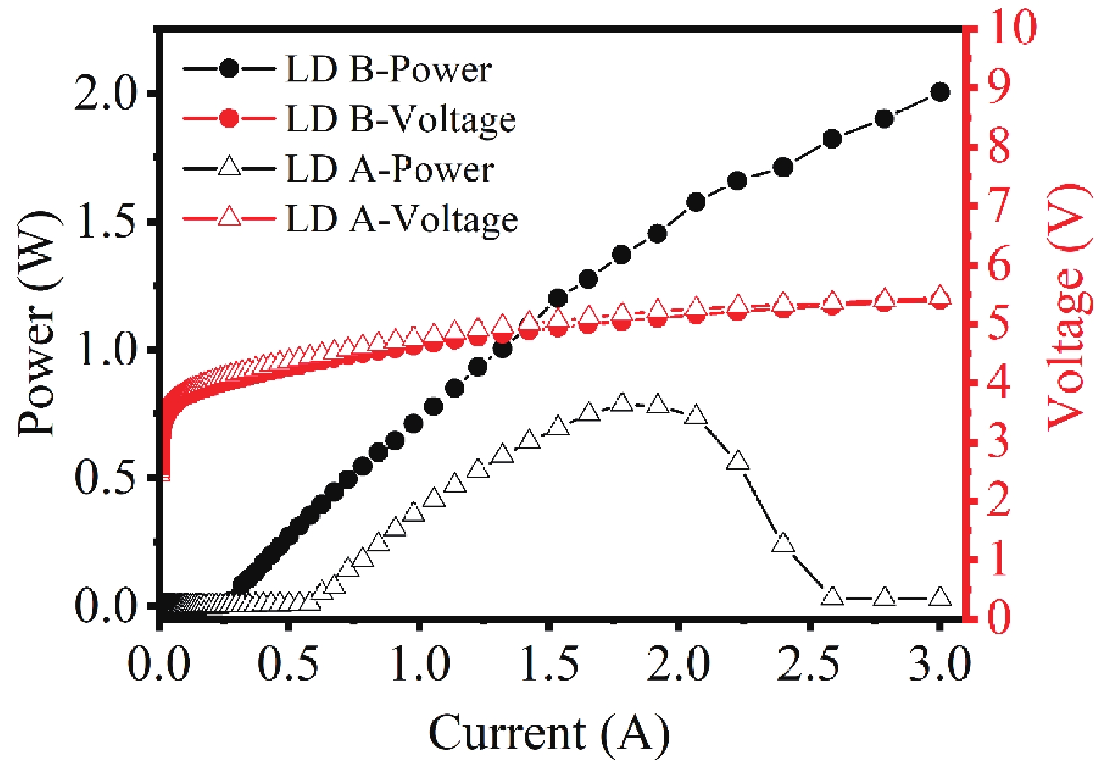
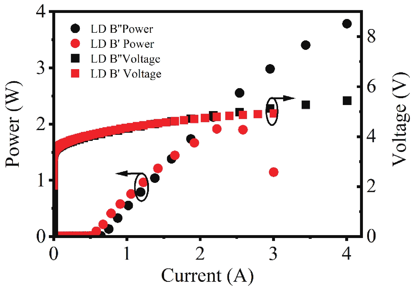
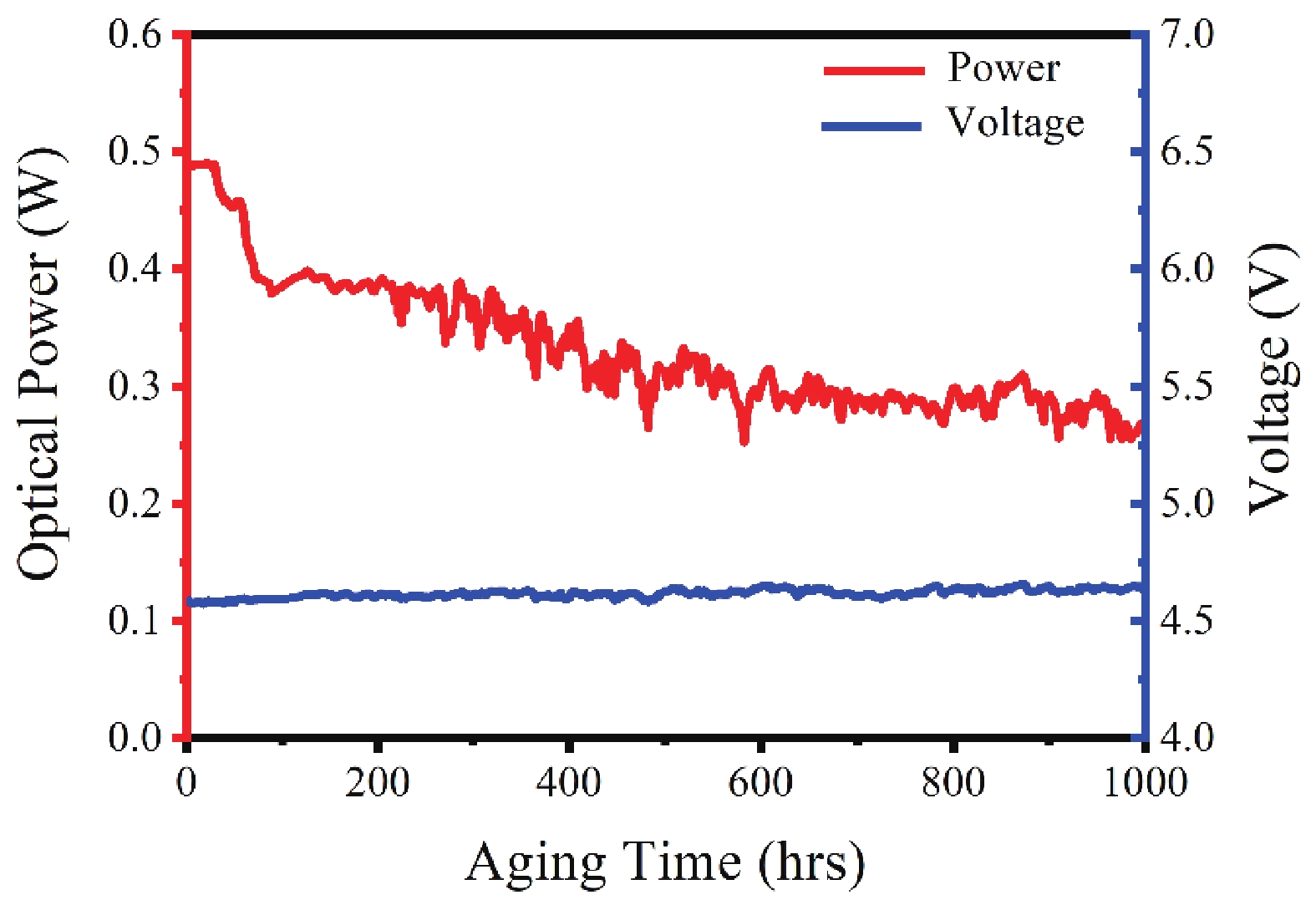
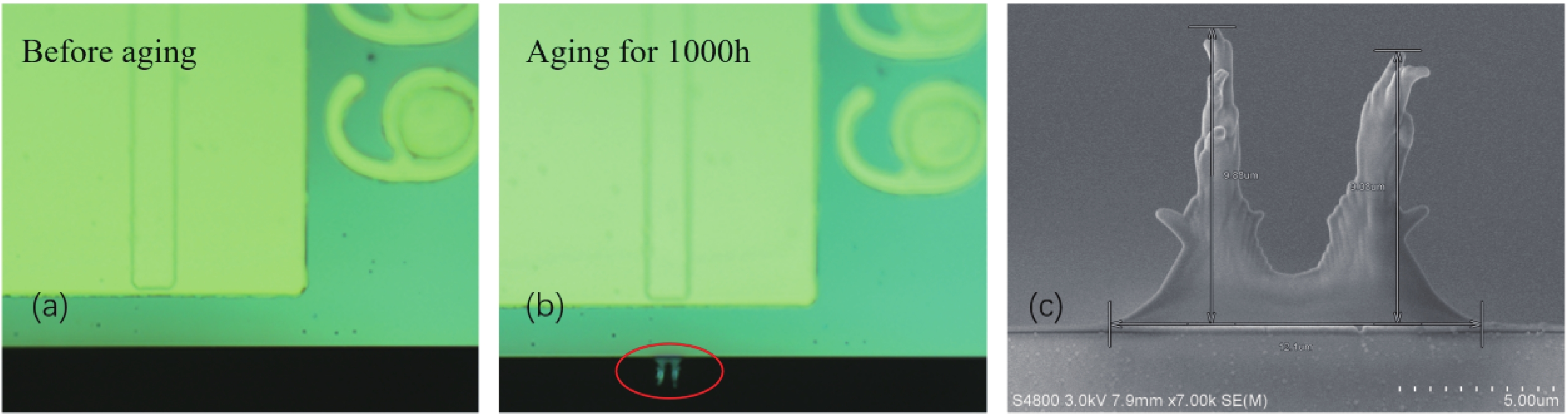
In the past few years, many groups have focused on the research and development of GaN-based ultraviolet laser diodes (UV LDs). Great progresses have been achieved even though many challenges exist. In this article, we analyze the challenges of developing GaN-based ultraviolet laser diodes, and the approaches to improve the performance of ultraviolet laser diode are reviewed. With these techniques, room temperature (RT) pulsed oscillation of AlGaN UVA (ultraviolet A) LD has been realized, with a lasing wavelength of 357.9 nm. Combining with the suppression of thermal effect, the high output power of 3.8 W UV LD with a lasing wavelength of 386.5 nm was also fabricated.


J. Semicond.
2024, 45(1): 012101 doi: 10.1088/1674-4926/45/1/012101
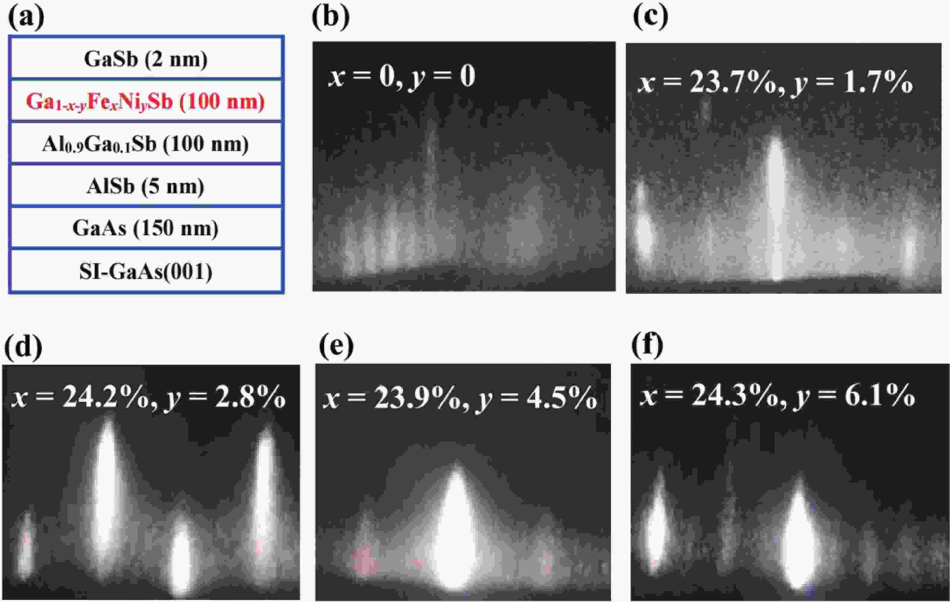
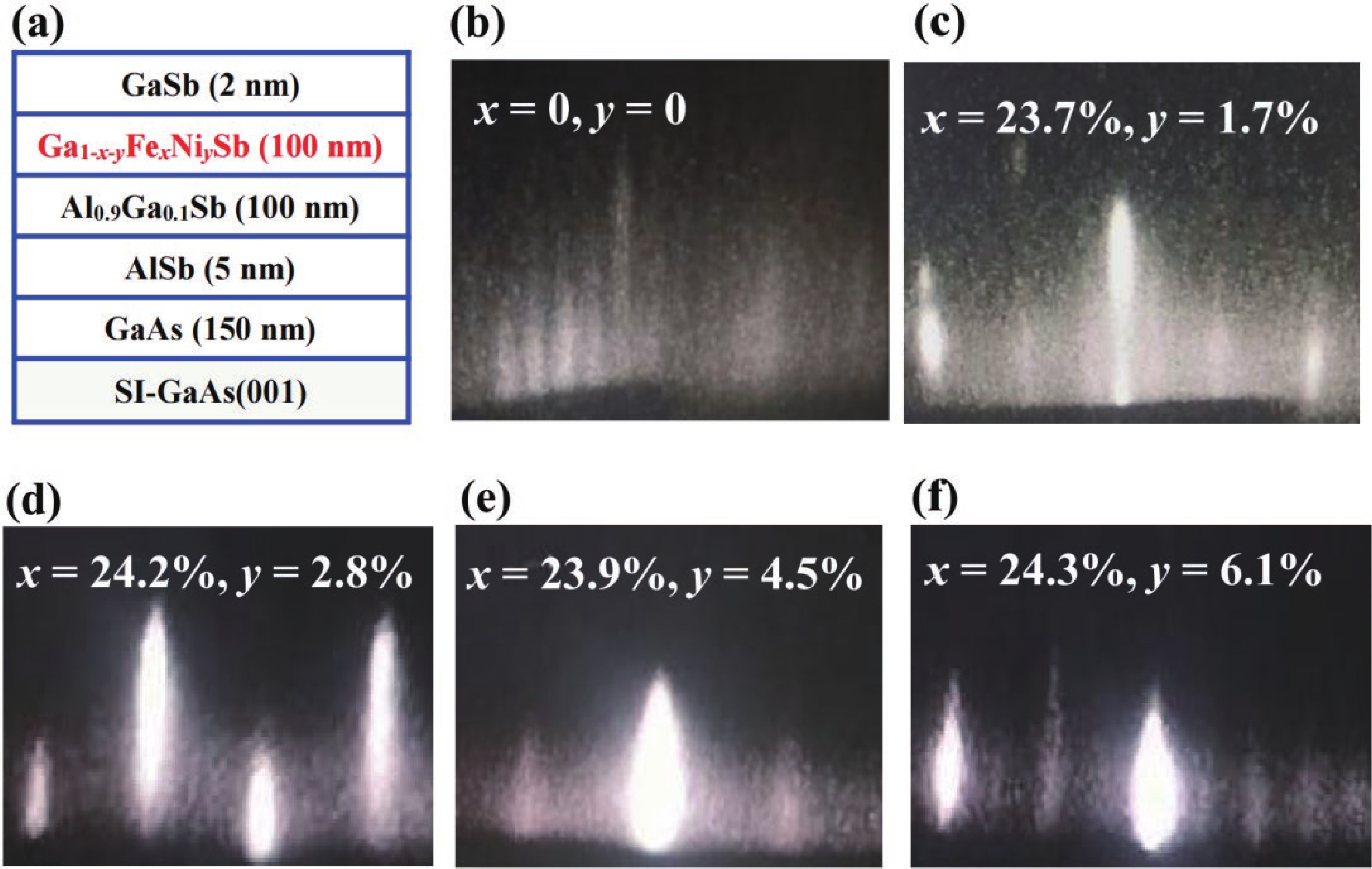
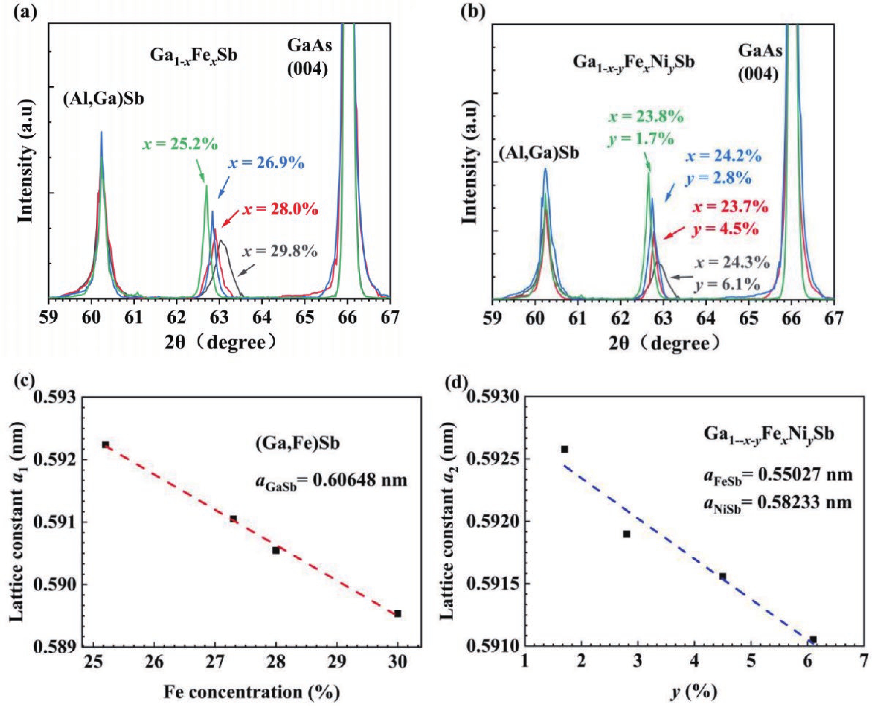
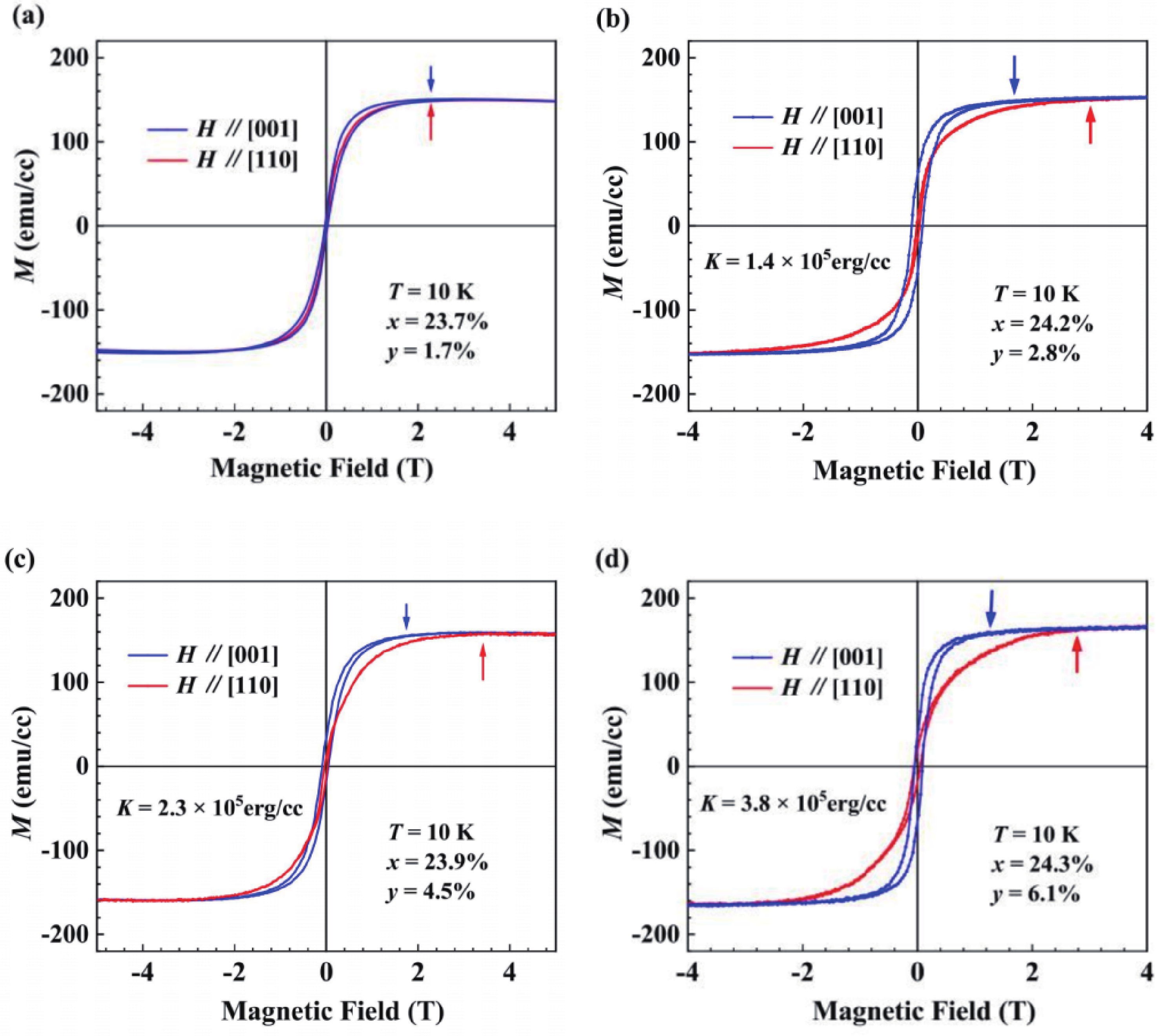
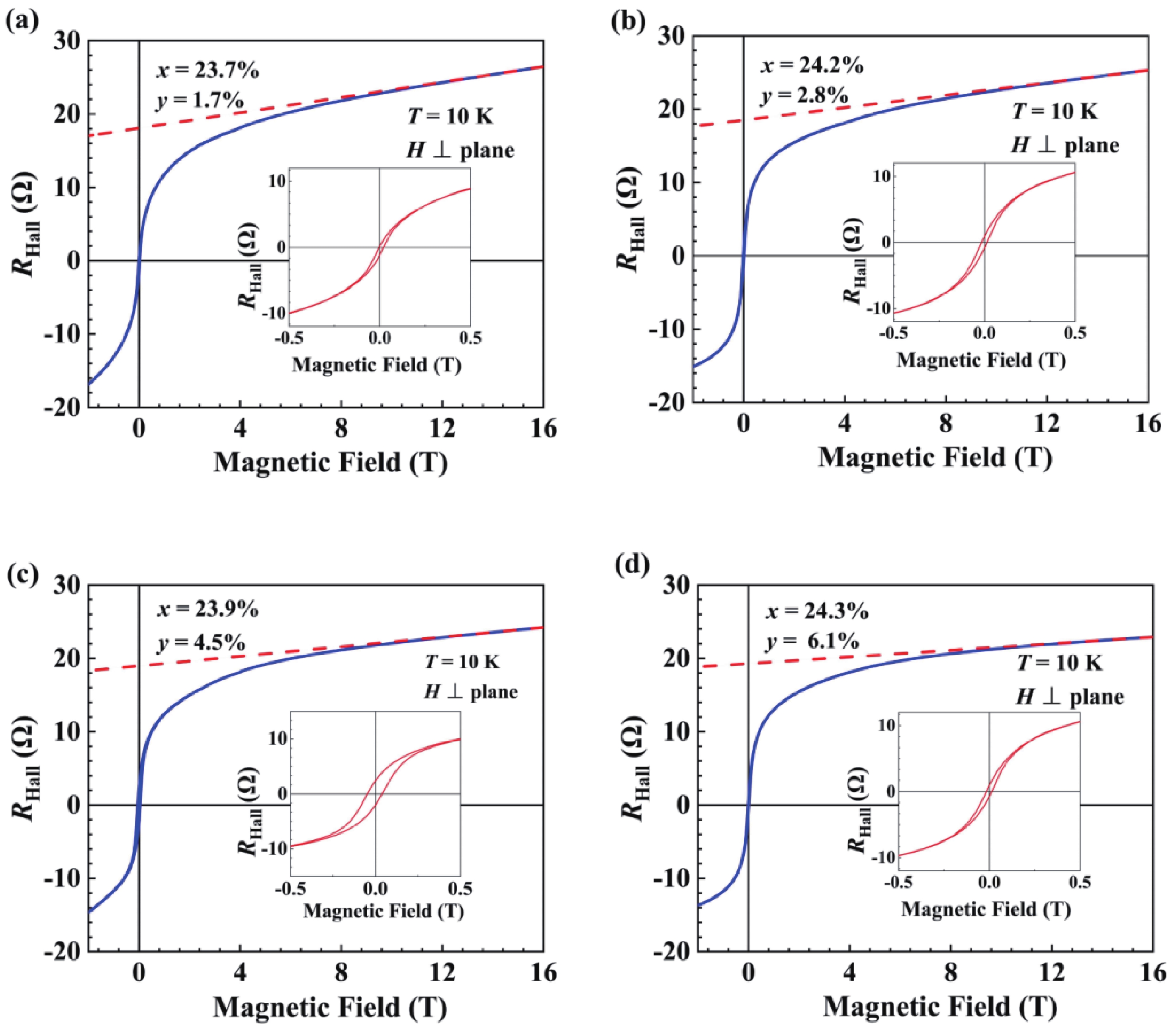
(Ga,Fe)Sb is a promising magnetic semiconductor (MS) for spintronic applications because its Curie temperature (TC) is above 300 K when the Fe concentration is higher than 20%. However, the anisotropy constant Ku of (Ga,Fe)Sb is below 7.6 × 10³ erg/cm3 when Fe concentration is lower than 30%, which is one order of magnitude lower than that of (Ga,Mn)As. To address this issue, we grew Ga1-x-yFexNiySb films with almost the same x (≈24%) and different y to characterize their magnetic and electrical transport properties. We found that the magnetic anisotropy of Ga0.76-yFe0.24NiySb can be enhanced by increasing y, in which Ku is negligible at y = 1.7% but increases to 3.8 × 10⁵ erg/cm3 at y = 6.1% (TC = 354 K). In addition, the hole mobility (µ) of Ga1-x-yFexNiySb reaches 31.3 cm2/(V∙s) at x = 23.7%, y = 1.7% (TC = 319 K), which is much higher than the mobility of Ga1-xFexSb at x = 25.2% (µ = 6.2 cm2/(V∙s)). Our results provide useful information for enhancing the magnetic anisotropy and hole mobility of (Ga,Fe)Sb by using Ni co-doping.

J. Semicond.
2024, 45(1): 012201 doi: 10.1088/1674-4926/45/1/012201
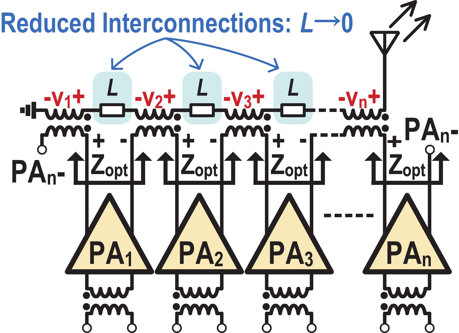
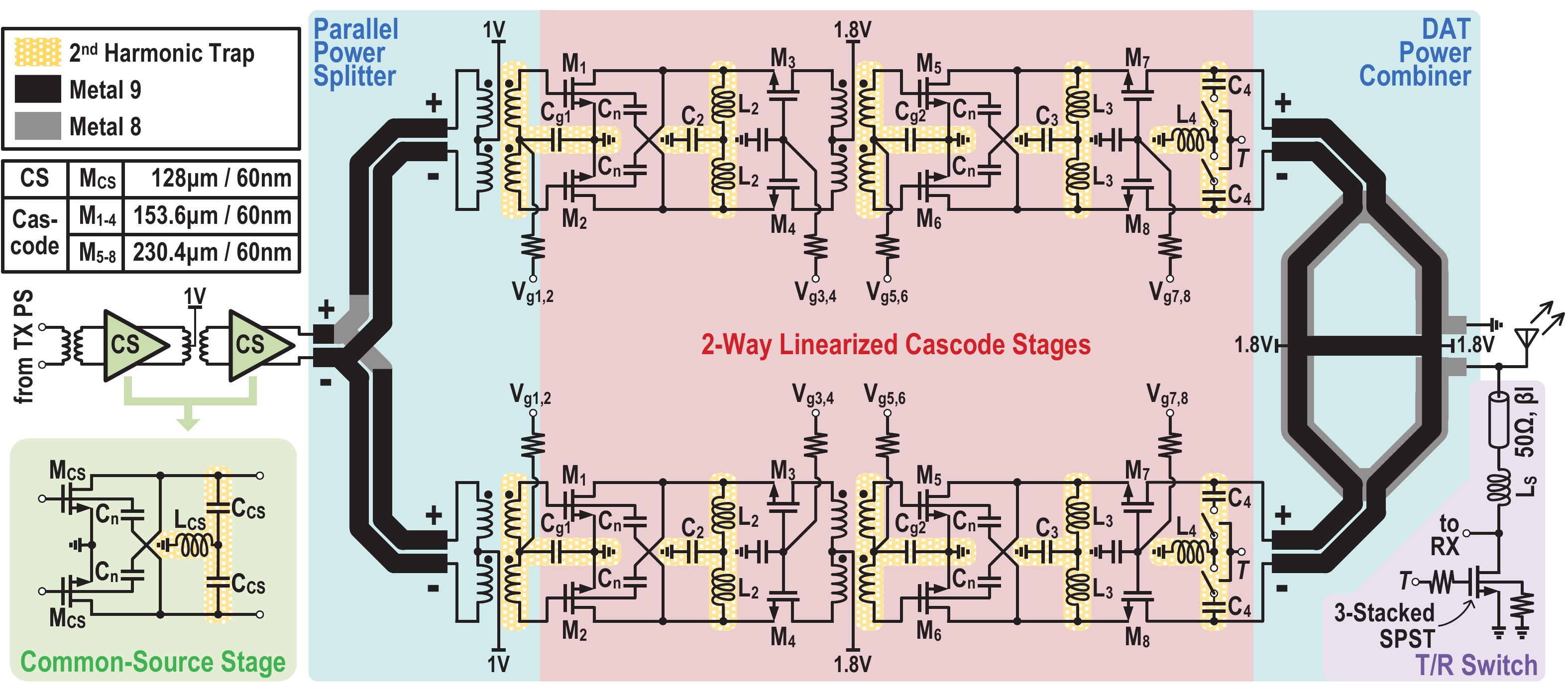
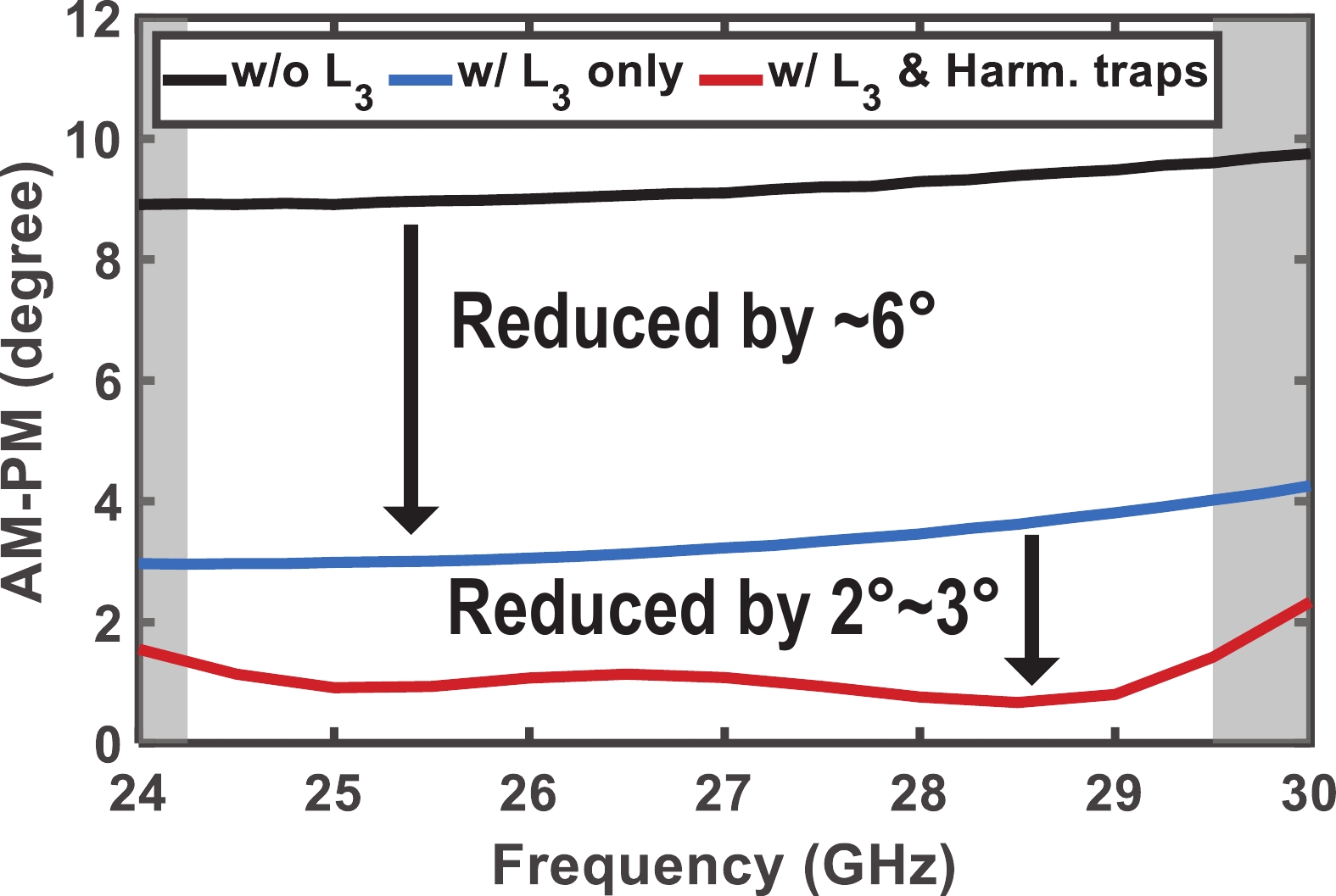
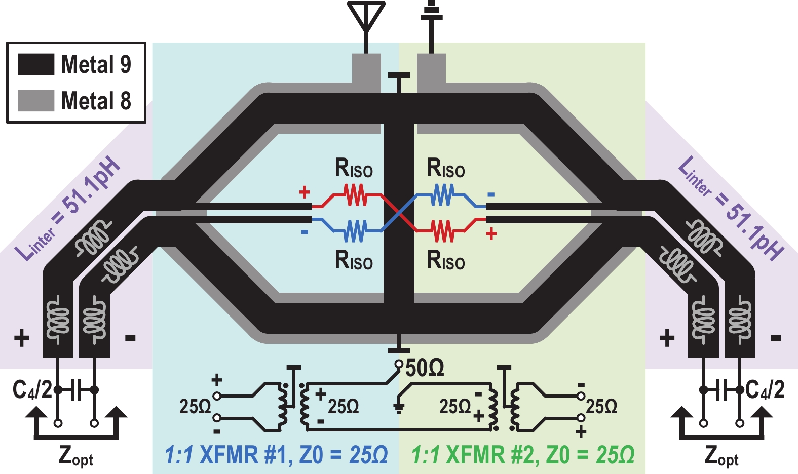
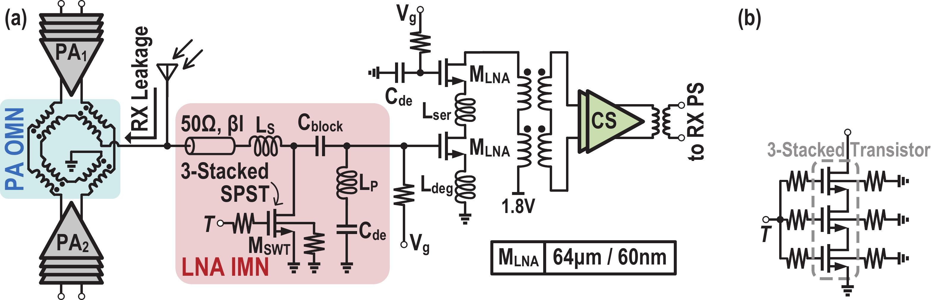
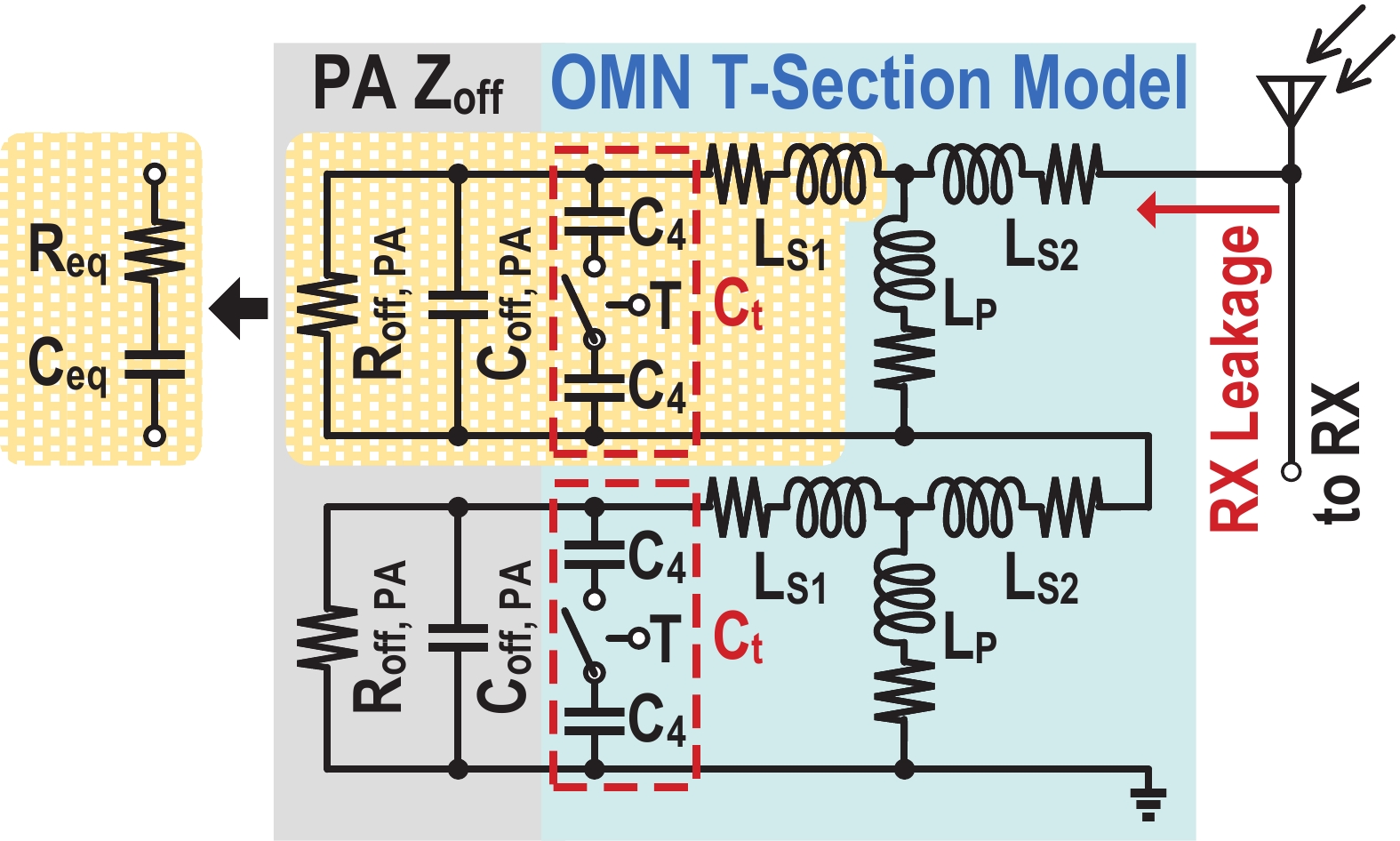
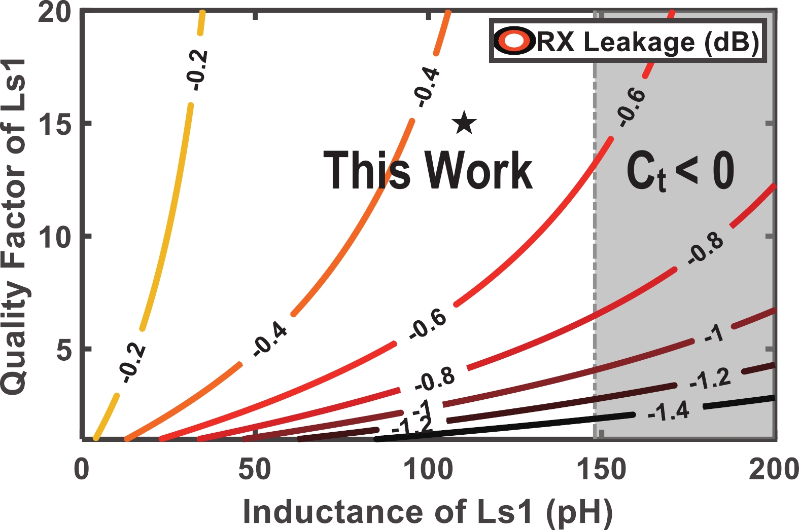
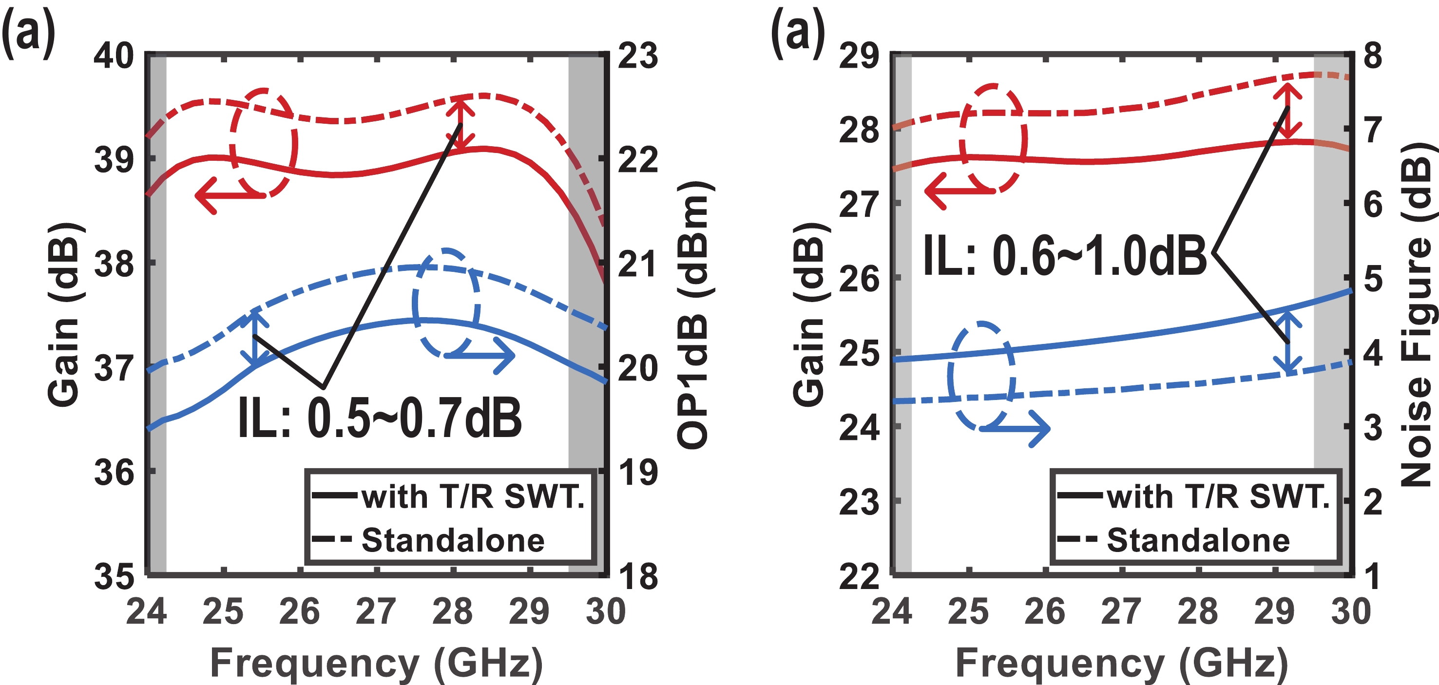
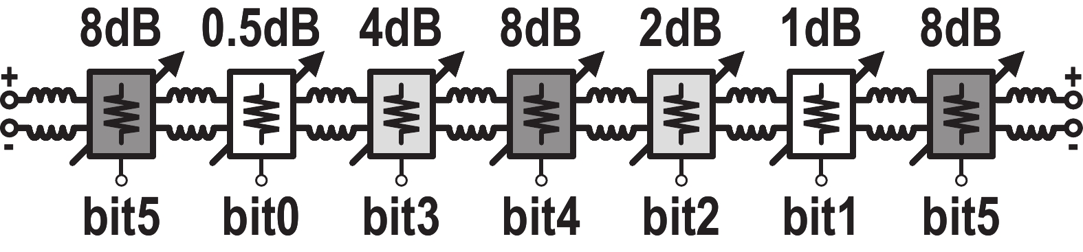
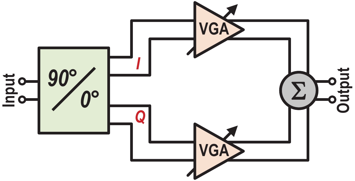
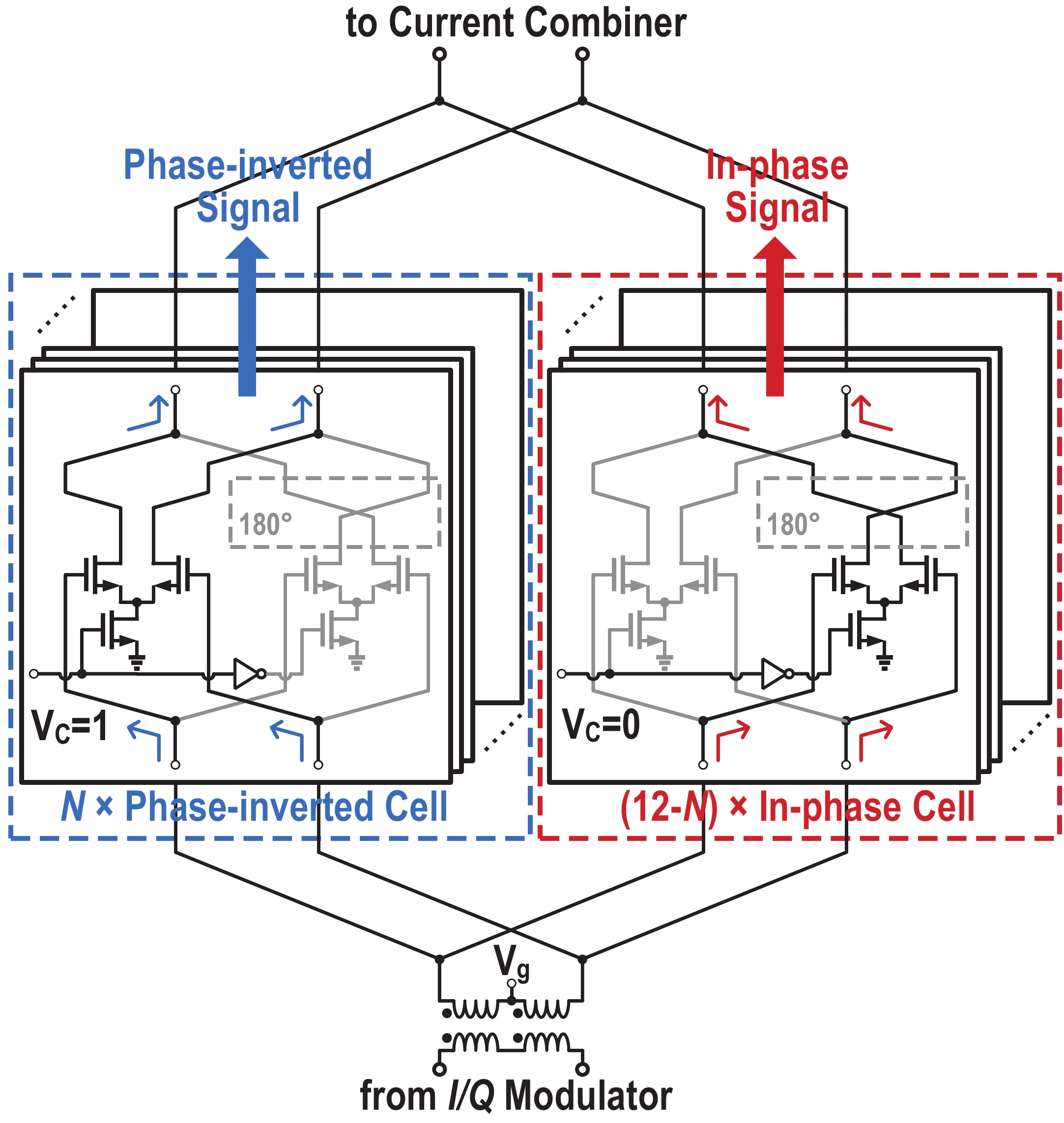
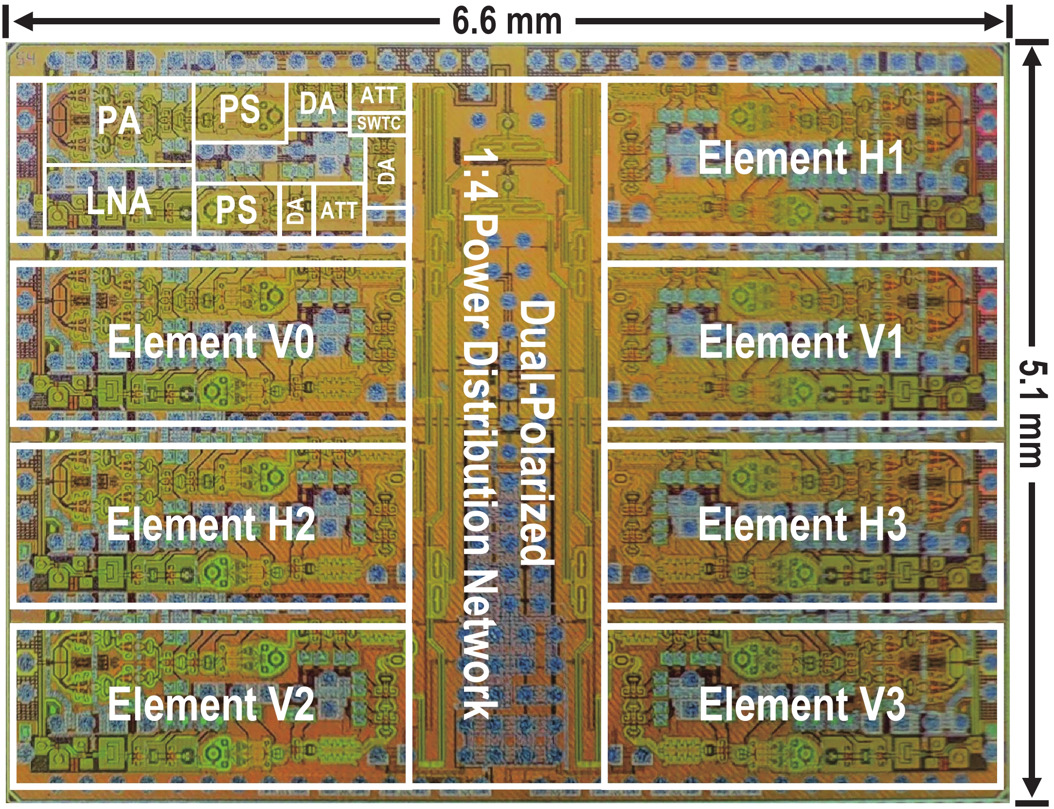
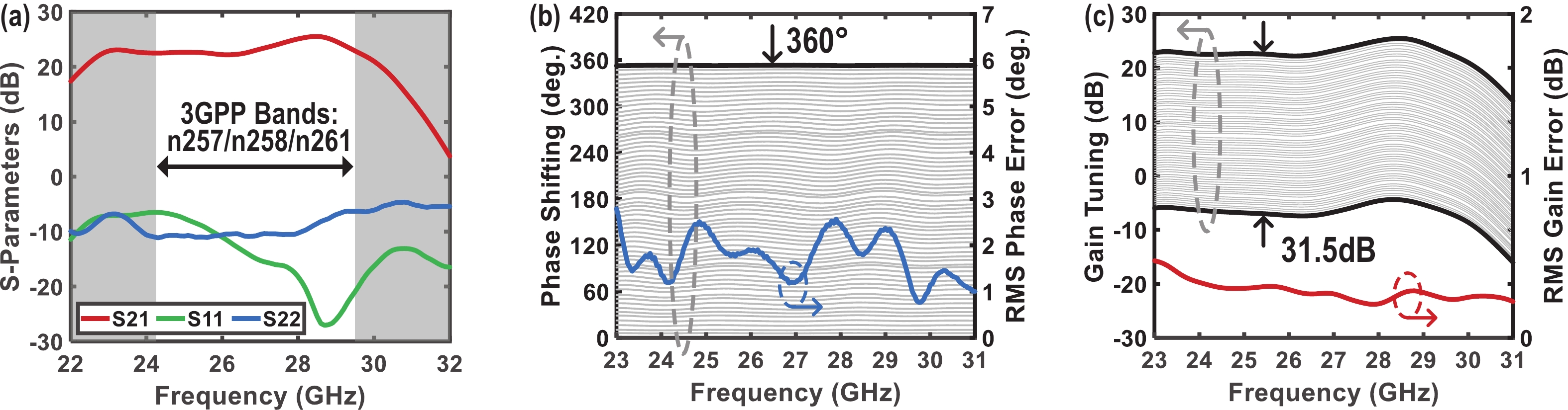
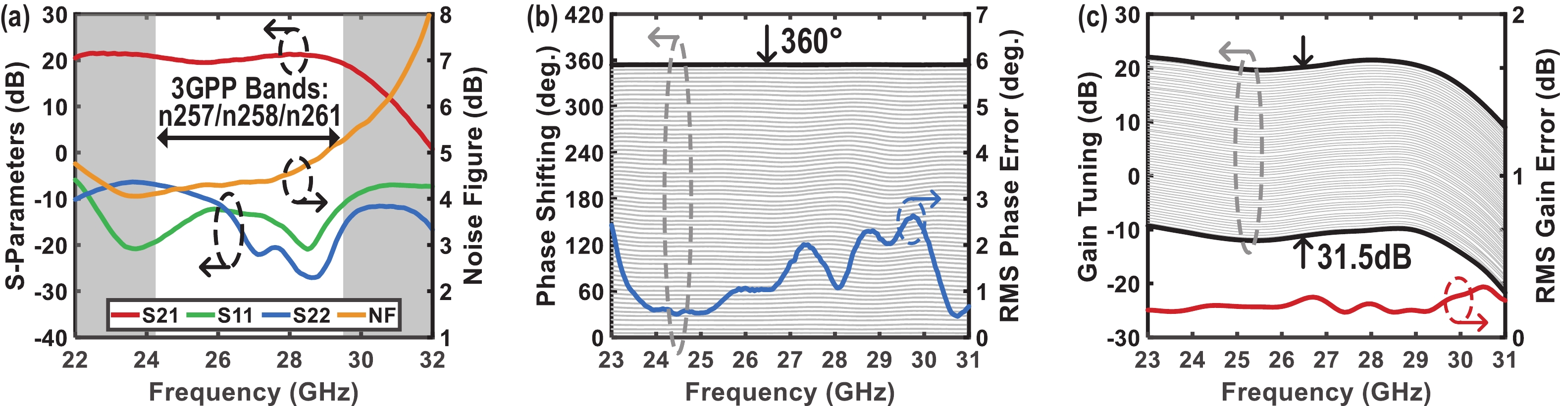
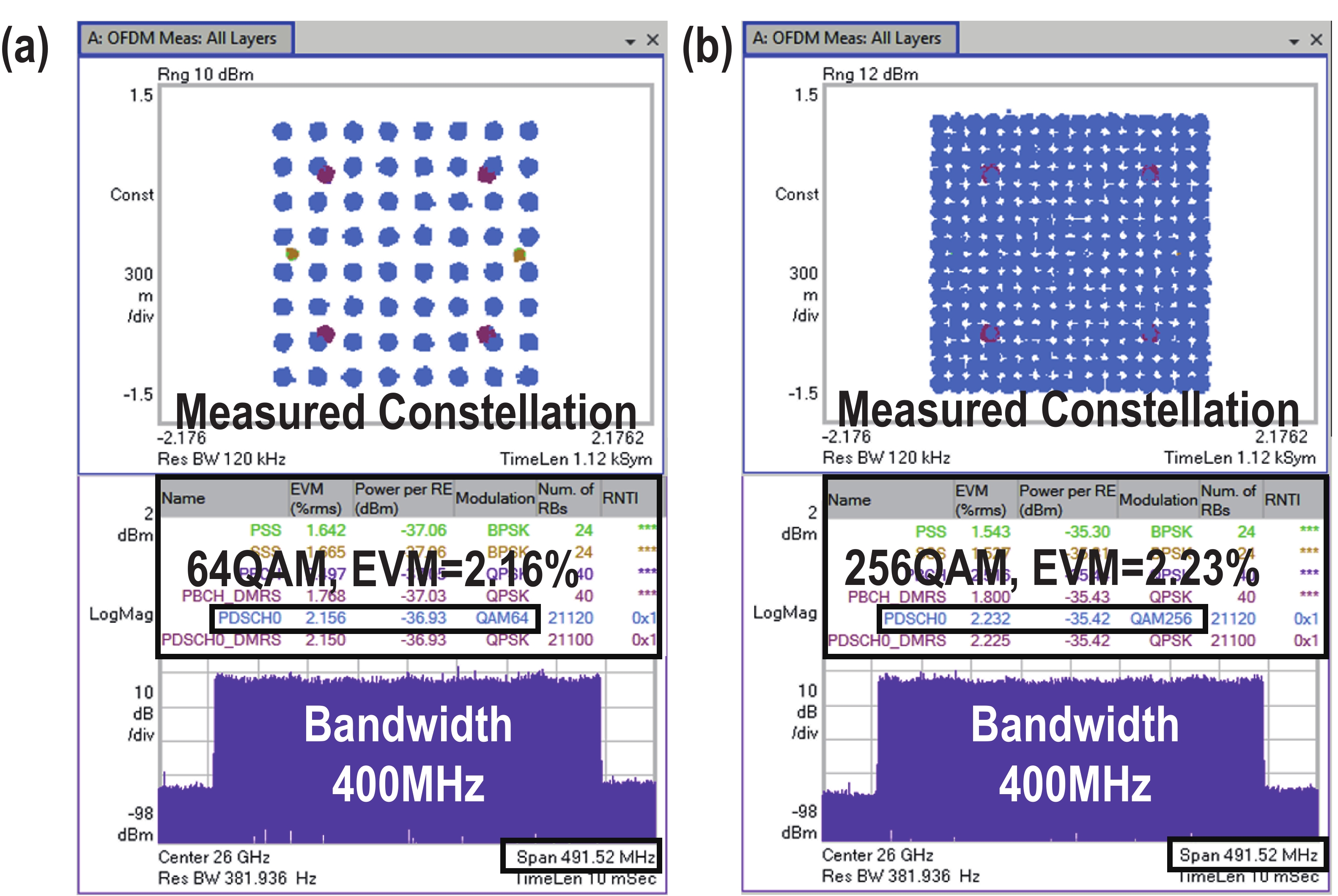
This article presents an 8-element dual-polarized phased-array transceiver (TRX) front-end IC for millimeter-wave (mm-Wave) 5G new radio (NR). Power enhancement technologies for power amplifiers (PA) in mm-Wave 5G phased-array TRX are discussed. A four-stage wideband high-power class-AB PA with distributed-active-transformer (DAT) power combining and multi-stage second-harmonic traps is proposed, ensuring the mitigated amplitude-to-phase (AM-PM) distortions across wide carrier frequencies without degrading transmitting (TX) power, gain and efficiency. TX and receiving (RX) switching is achieved by a matching network co-designed on-chip T/R switch. In each TRX element, 6-bit 360° phase shifting and 6-bit 31.5-dB gain tuning are respectively achieved by the digital-controlled vector-modulated phase shifter (VMPS) and differential attenuator (ATT). Fabricated in 65-nm bulk complementary metal oxide semiconductor (CMOS), the proposed TRX demonstrates the measured peak TX/RX gains of 25.5/21.3 dB, covering the 24−29.5 GHz band. The measured peak TX OP1dB and power-added efficiency (PAE) are 20.8 dBm and 21.1%, respectively. The measured minimum RX NF is 4.1 dB. The TRX achieves an output power of 11.0−12.4 dBm and error vector magnitude (EVM) of 5% with 400-MHz 5G NR FR2 OFDM 64-QAM signals across 24−29.5 GHz, covering 3GPP 5G NR FR2 operating bands of n257, n258, and n261.


J. Semicond.
2024, 45(1): 012301 doi: 10.1088/1674-4926/45/1/012301
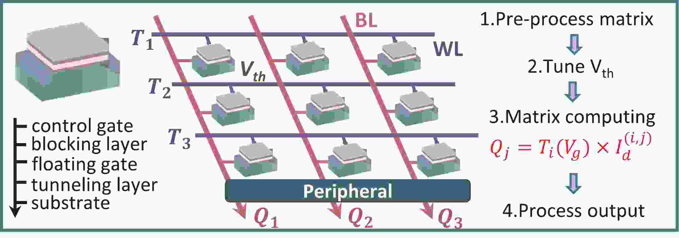
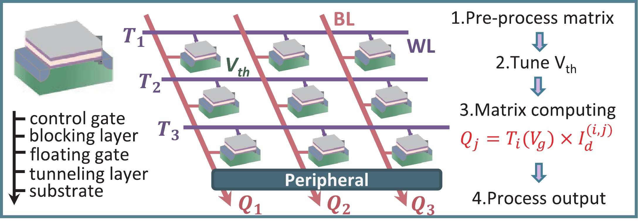
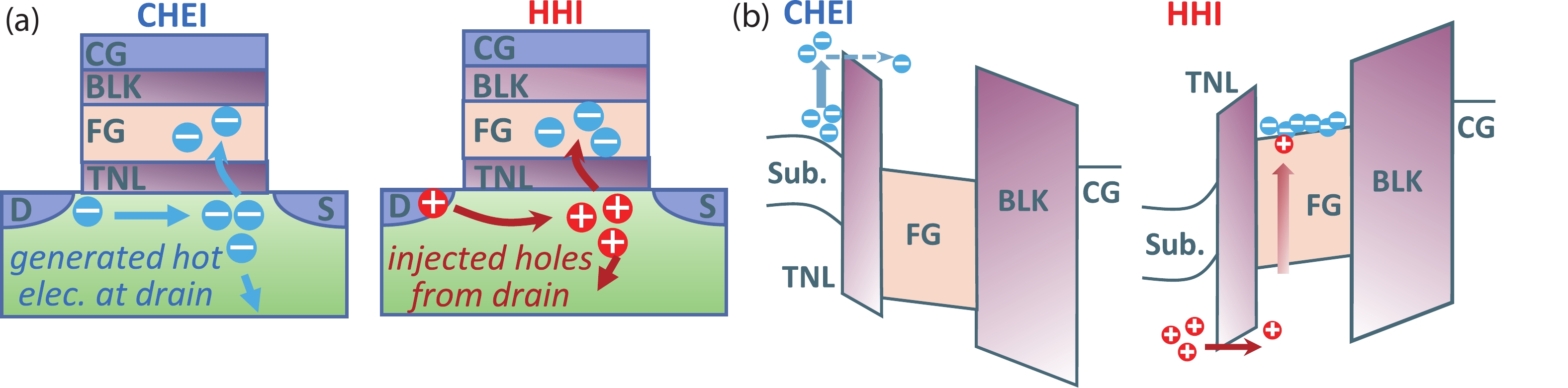
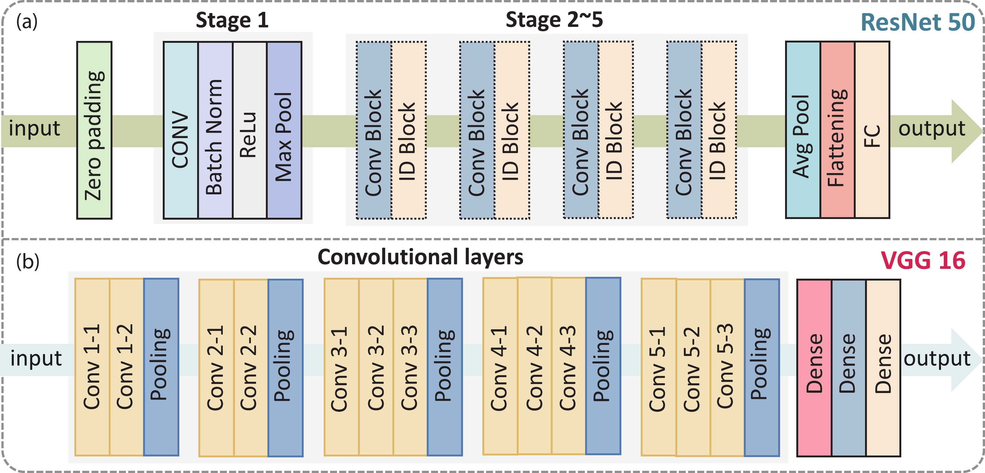
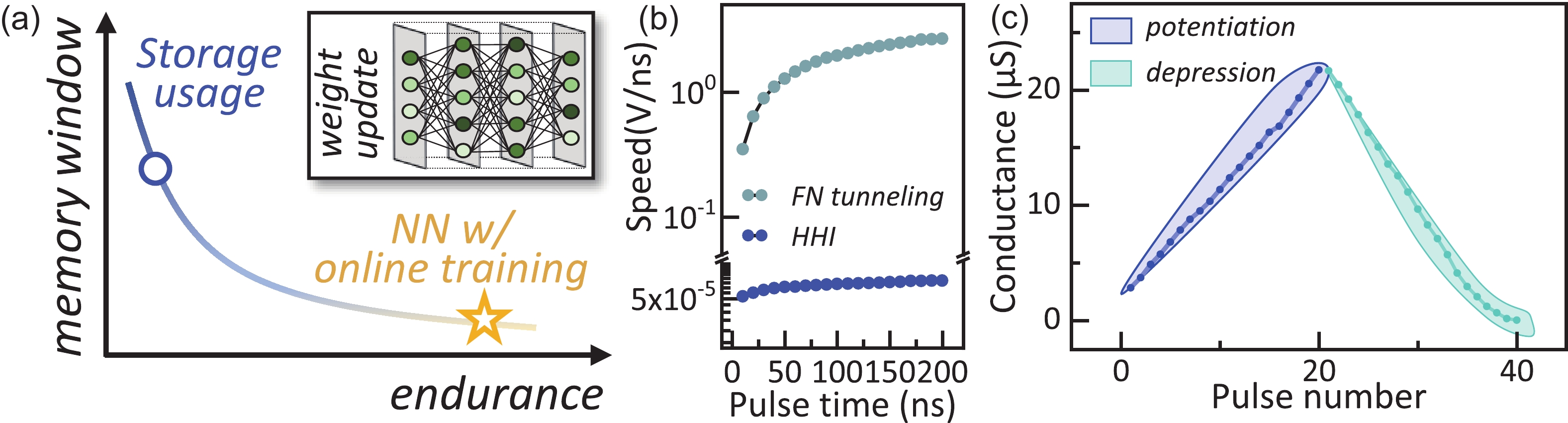
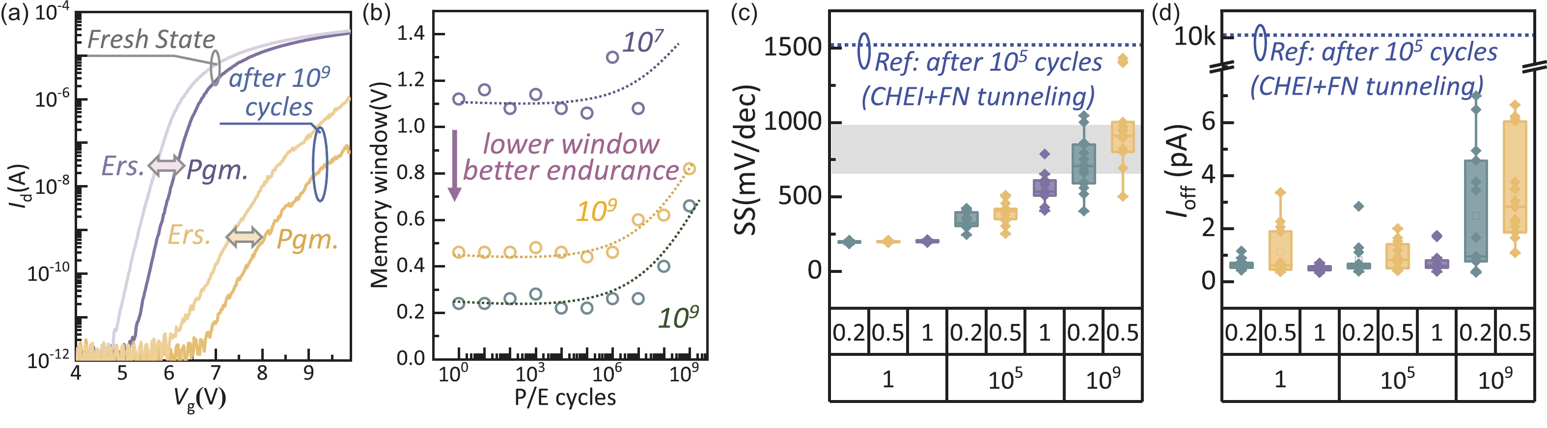
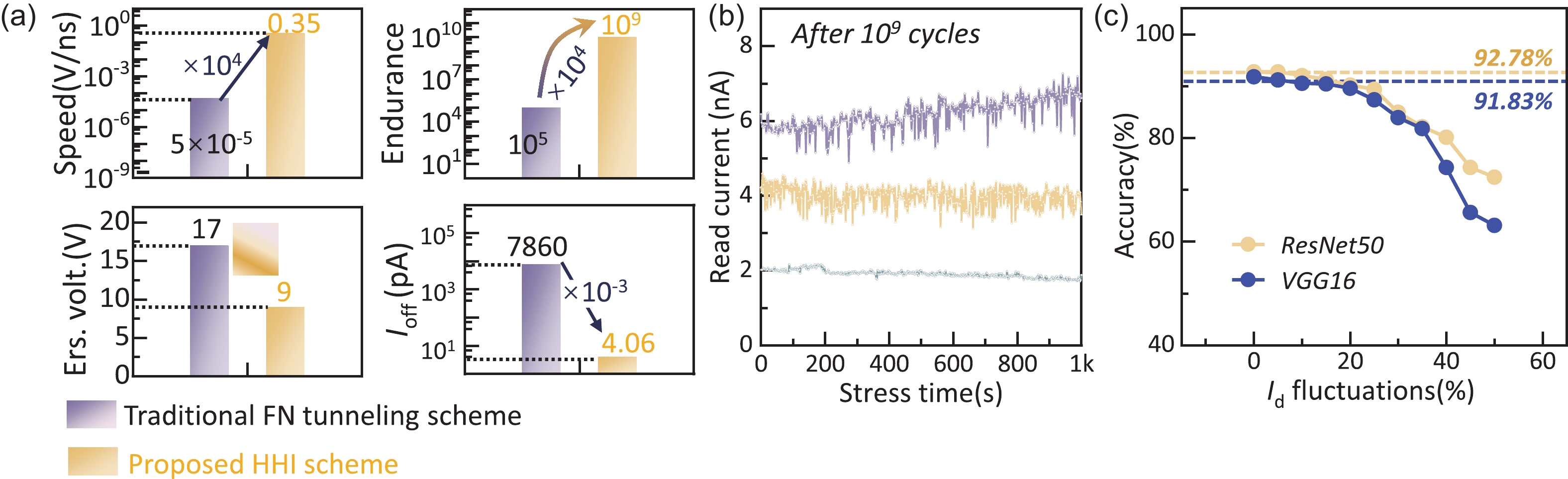
With the rapid development of machine learning, the demand for high-efficient computing becomes more and more urgent. To break the bottleneck of the traditional Von Neumann architecture, computing-in-memory (CIM) has attracted increasing attention in recent years. In this work, to provide a feasible CIM solution for the large-scale neural networks (NN) requiring continuous weight updating in online training, a flash-based computing-in-memory with high endurance (109 cycles) and ultra-fast programming speed is investigated. On the one hand, the proposed programming scheme of channel hot electron injection (CHEI) and hot hole injection (HHI) demonstrate high linearity, symmetric potentiation, and a depression process, which help to improve the training speed and accuracy. On the other hand, the low-damage programming scheme and memory window (MW) optimizations can suppress cell degradation effectively with improved computing accuracy. Even after 109 cycles, the leakage current (Ioff) of cells remains sub-10pA, ensuring the large-scale computing ability of memory. Further characterizations are done on read disturb to demonstrate its robust reliabilities. By processing CIFAR-10 tasks, it is evident that ~90% accuracy can be achieved after 109 cycles in both ResNet50 and VGG16 NN. Our results suggest that flash-based CIM has great potential to overcome the limitations of traditional Von Neumann architectures and enable high-performance NN online training, which pave the way for further development of artificial intelligence (AI) accelerators.
J. Semicond.
2024, 45(1): 012501 doi: 10.1088/1674-4926/45/1/012501
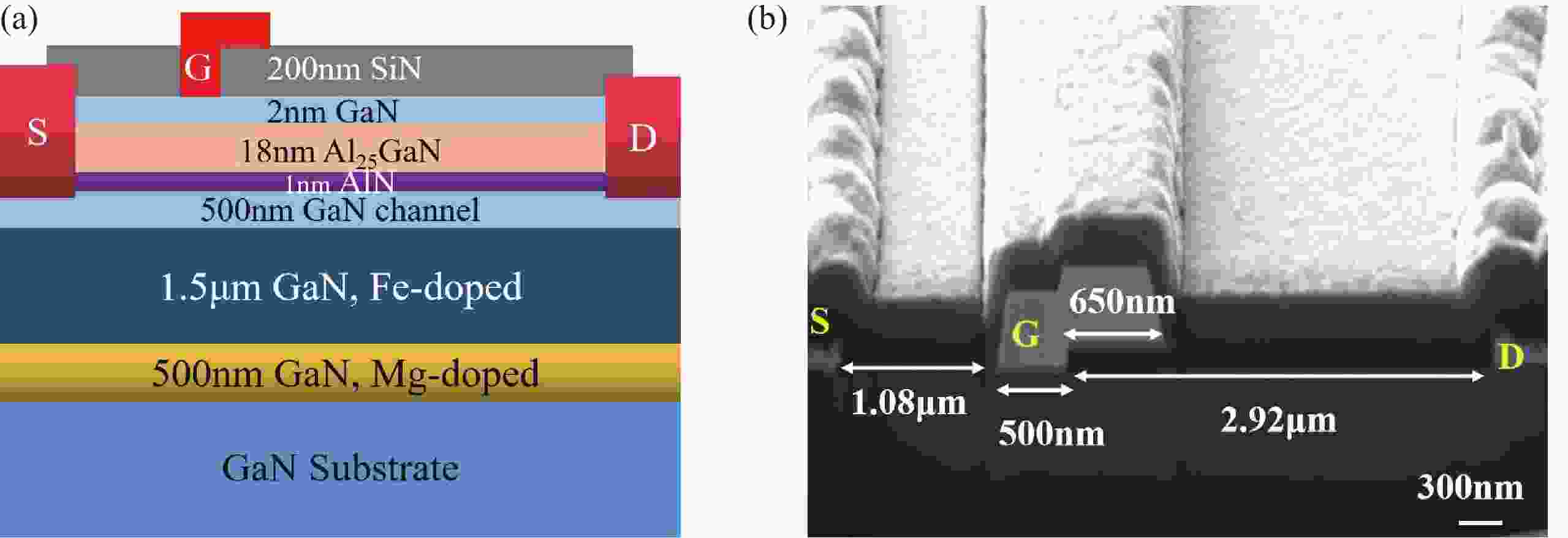
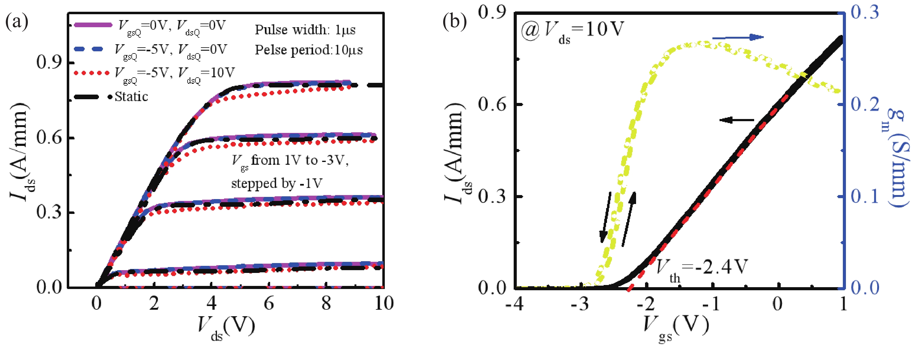
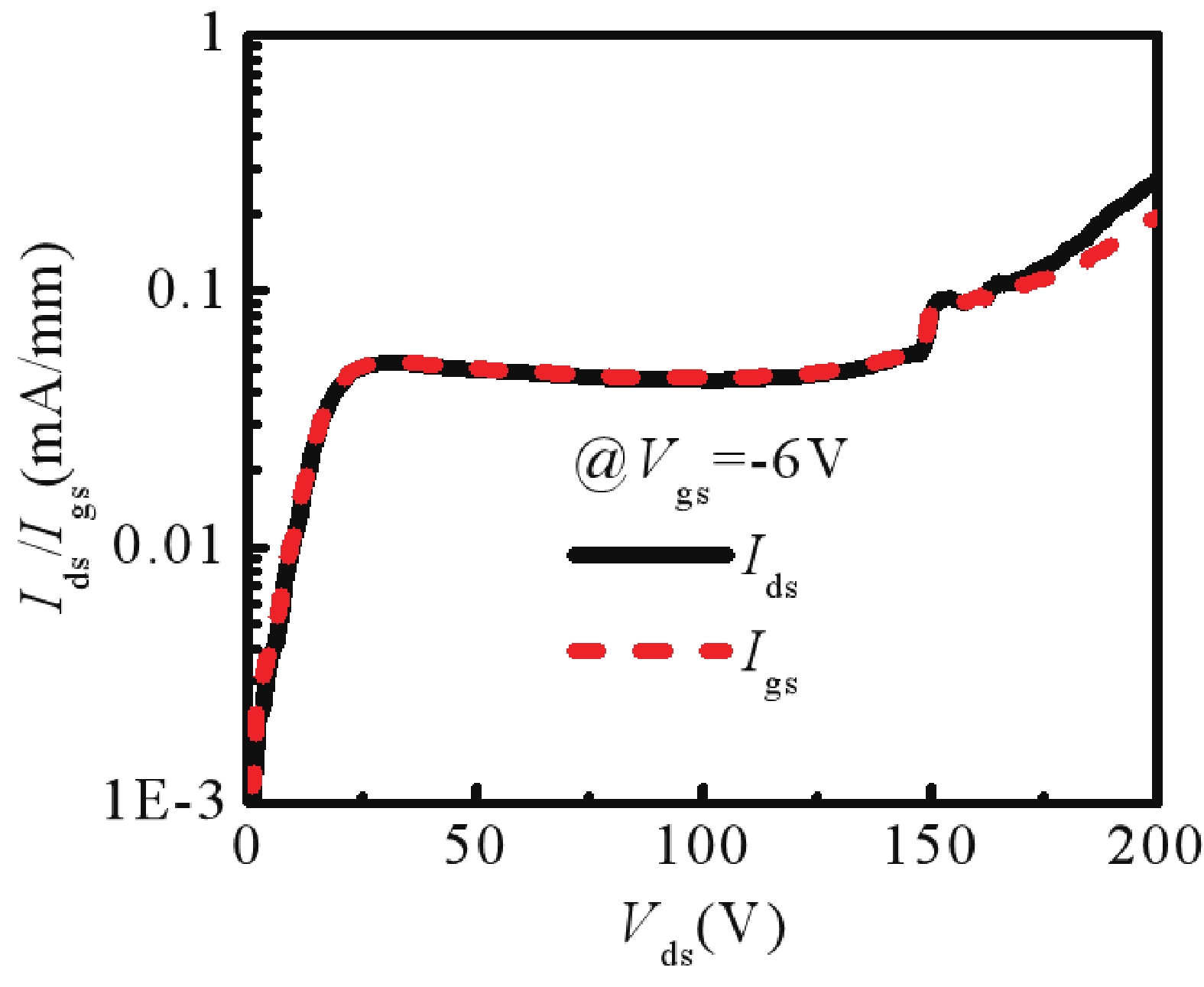
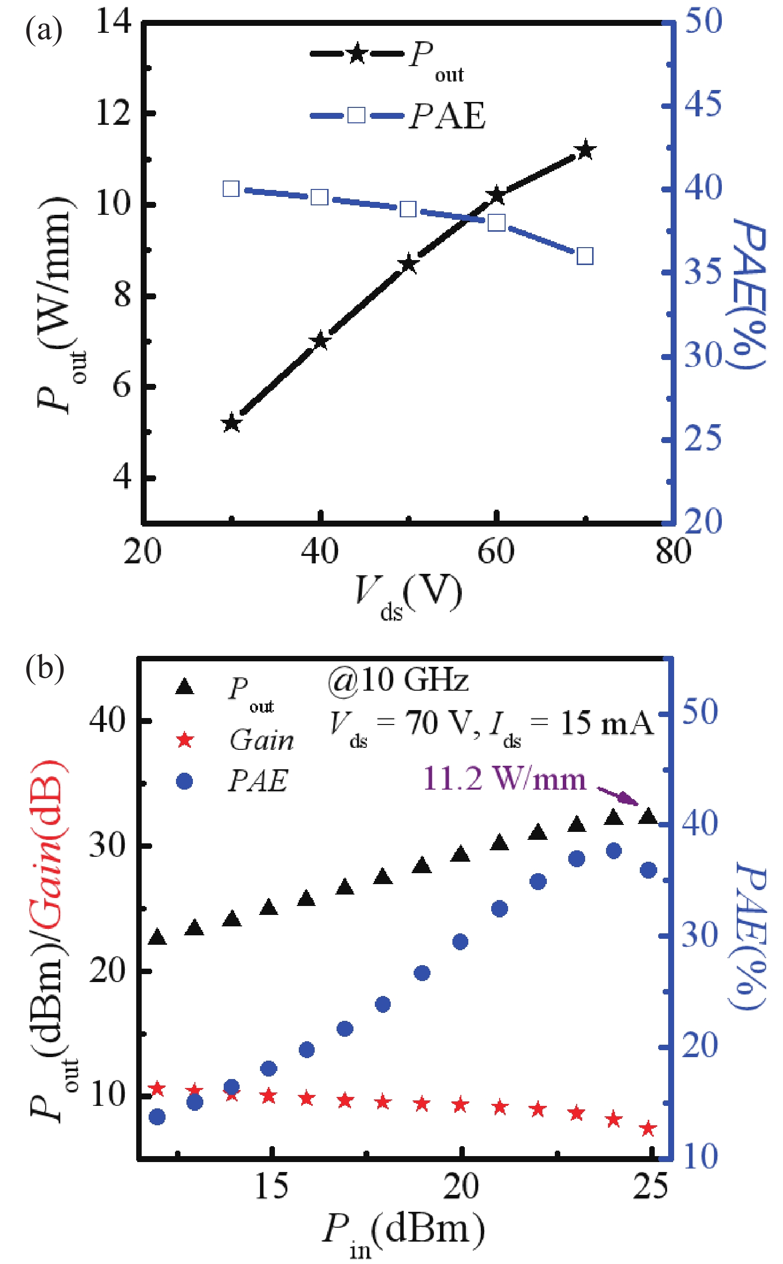
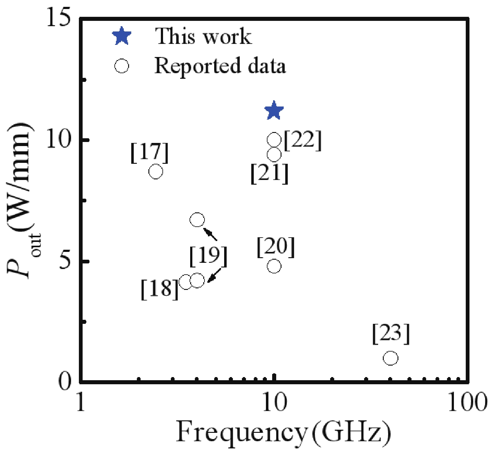
In this letter, high power density AlGaN/GaN high electron-mobility transistors (HEMTs) on a freestanding GaN substrate are reported. An asymmetric Γ-shaped 500-nm gate with a field plate of 650 nm is introduced to improve microwave power performance. The breakdown voltage (BV) is increased to more than 200 V for the fabricated device with gate-to-source and gate-to-drain distances of 1.08 and 2.92 μm. A record continuous-wave power density of 11.2 W/mm@10 GHz is realized with a drain bias of 70 V. The maximum oscillation frequency (fmax) and unity current gain cut-off frequency (ft) of the AlGaN/GaN HEMTs exceed 30 and 20 GHz, respectively. The results demonstrate the potential of AlGaN/GaN HEMTs on free-standing GaN substrates for microwave power applications.

J. Semicond.
2024, 45(1): 012502 doi: 10.1088/1674-4926/45/1/012502
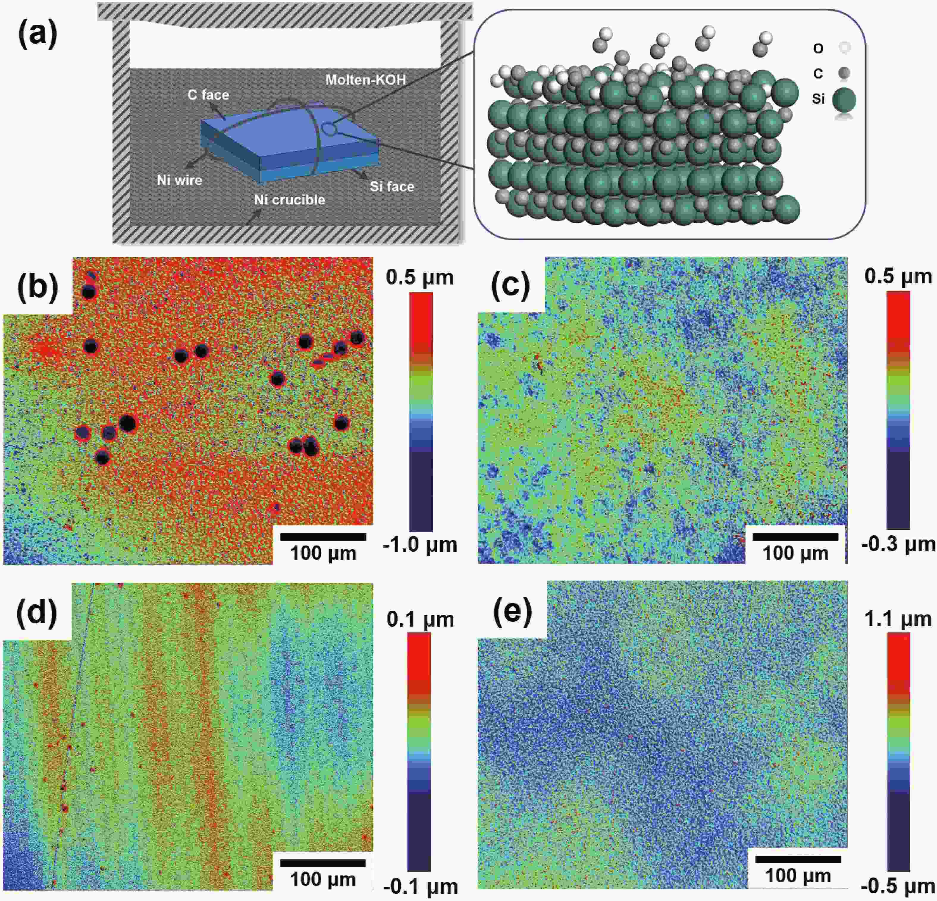
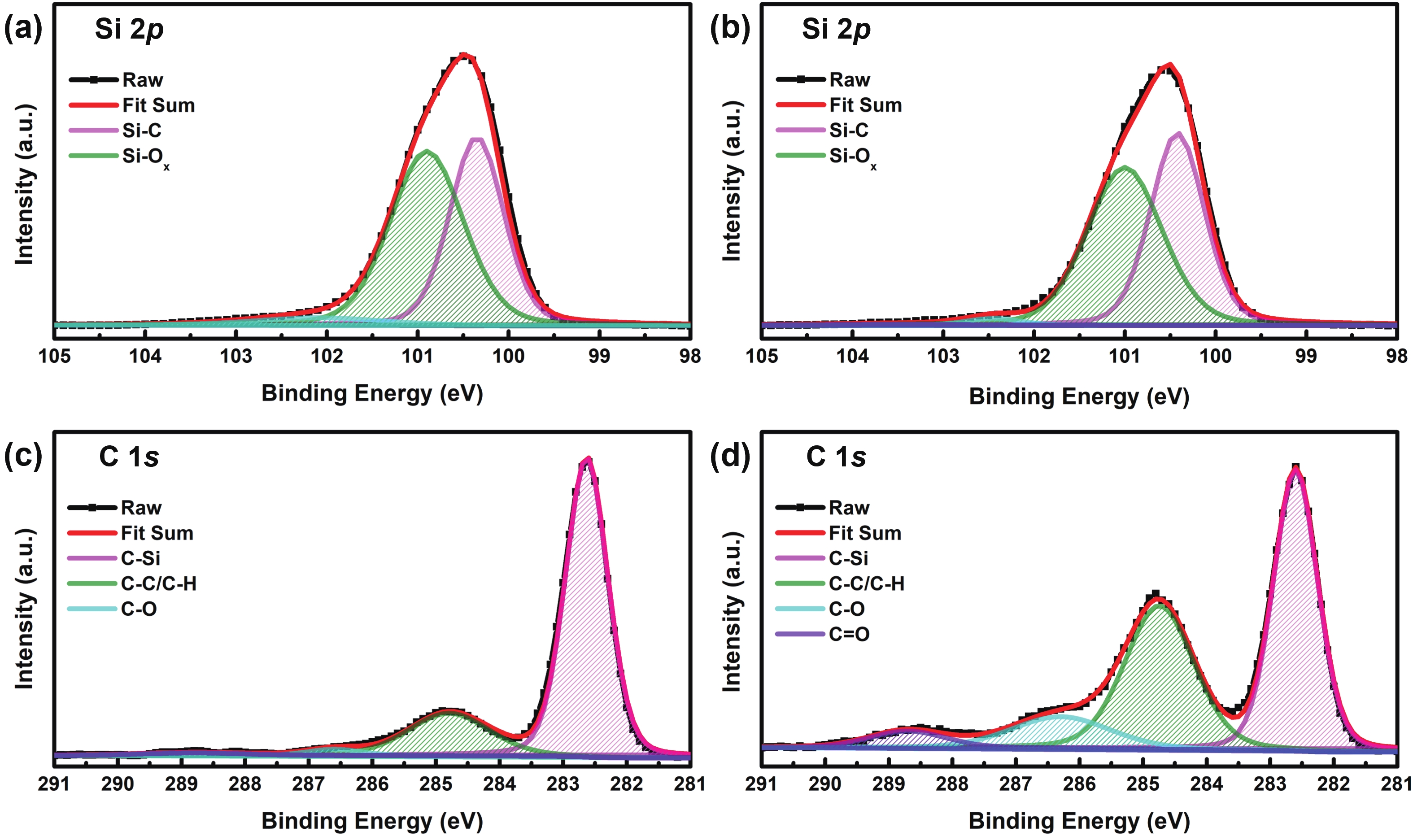
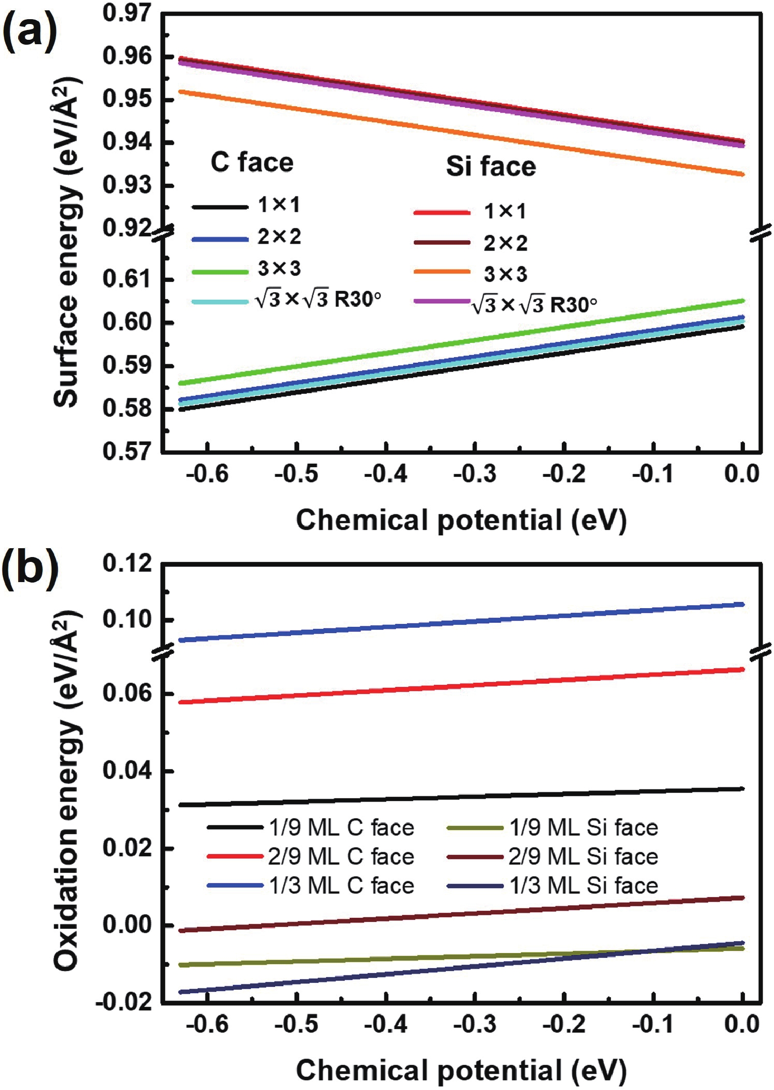
Molten-alkali etching has been widely used to reveal dislocations in 4H silicon carbide (4H-SiC), which has promoted the identification and statistics of dislocation density in 4H-SiC single crystals. However, the etching mechanism of 4H-SiC is limited misunderstood. In this letter, we reveal the anisotropic etching mechanism of the Si face and C face of 4H-SiC by combining molten-KOH etching, X-ray photoelectron spectroscopy (XPS) and first-principles investigations. The activation energies for the molten-KOH etching of the C face and Si face of 4H-SiC are calculated to be 25.09 and 35.75 kcal/mol, respectively. The molten-KOH etching rate of the C face is higher than the Si face. Combining XPS analysis and first-principles calculations, we find that the molten-KOH etching of 4H-SiC is proceeded by the cycling of the oxidation of 4H-SiC by the dissolved oxygen and the removal of oxides by molten KOH. The faster etching rate of the C face is caused by the fact that the oxides on the C face are unstable, and easier to be removed with molten alkali, rather than the C face being easier to be oxidized.

J. Semicond.
2024, 45(1): 012503 doi: 10.1088/1674-4926/45/1/012503
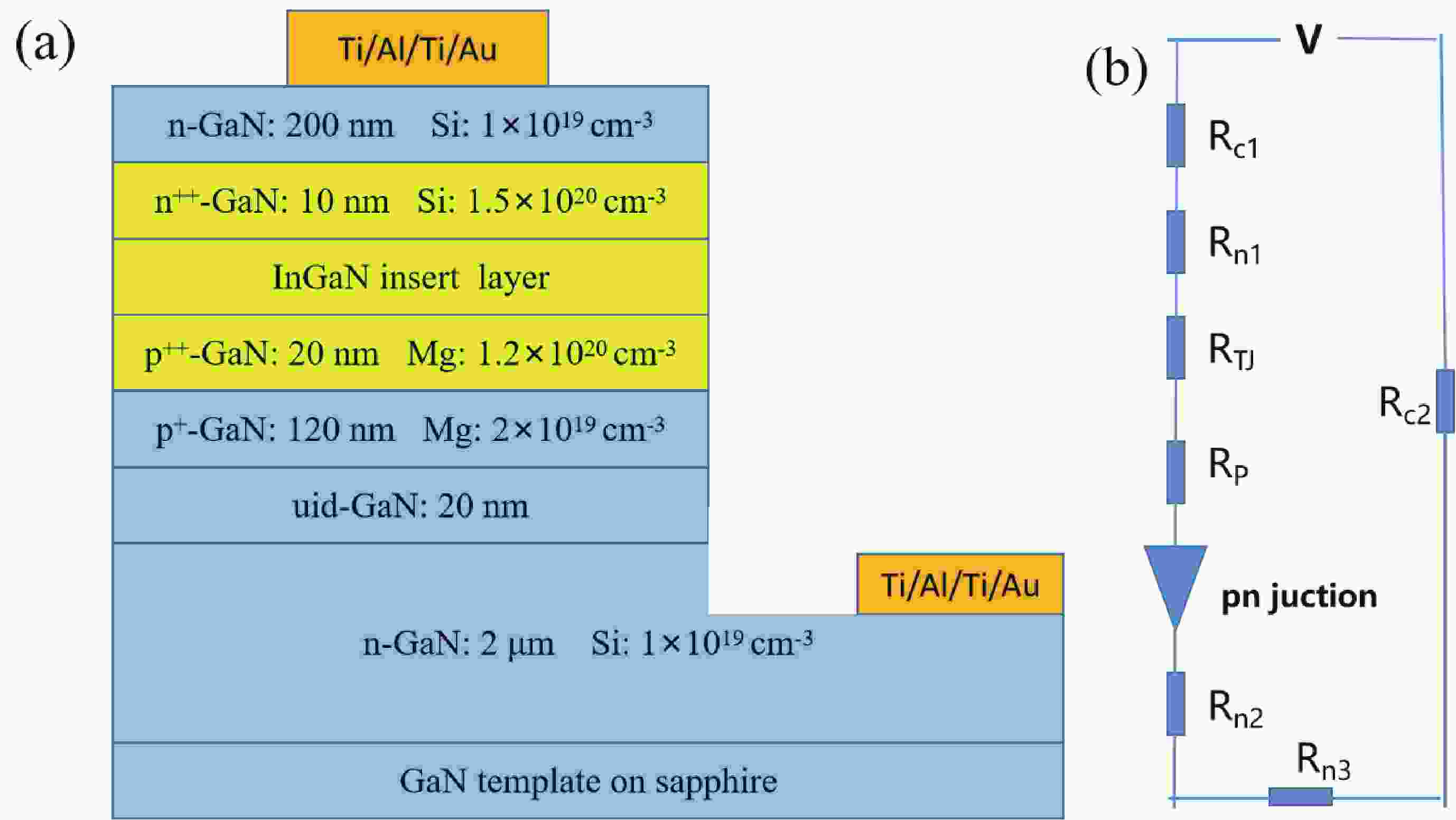
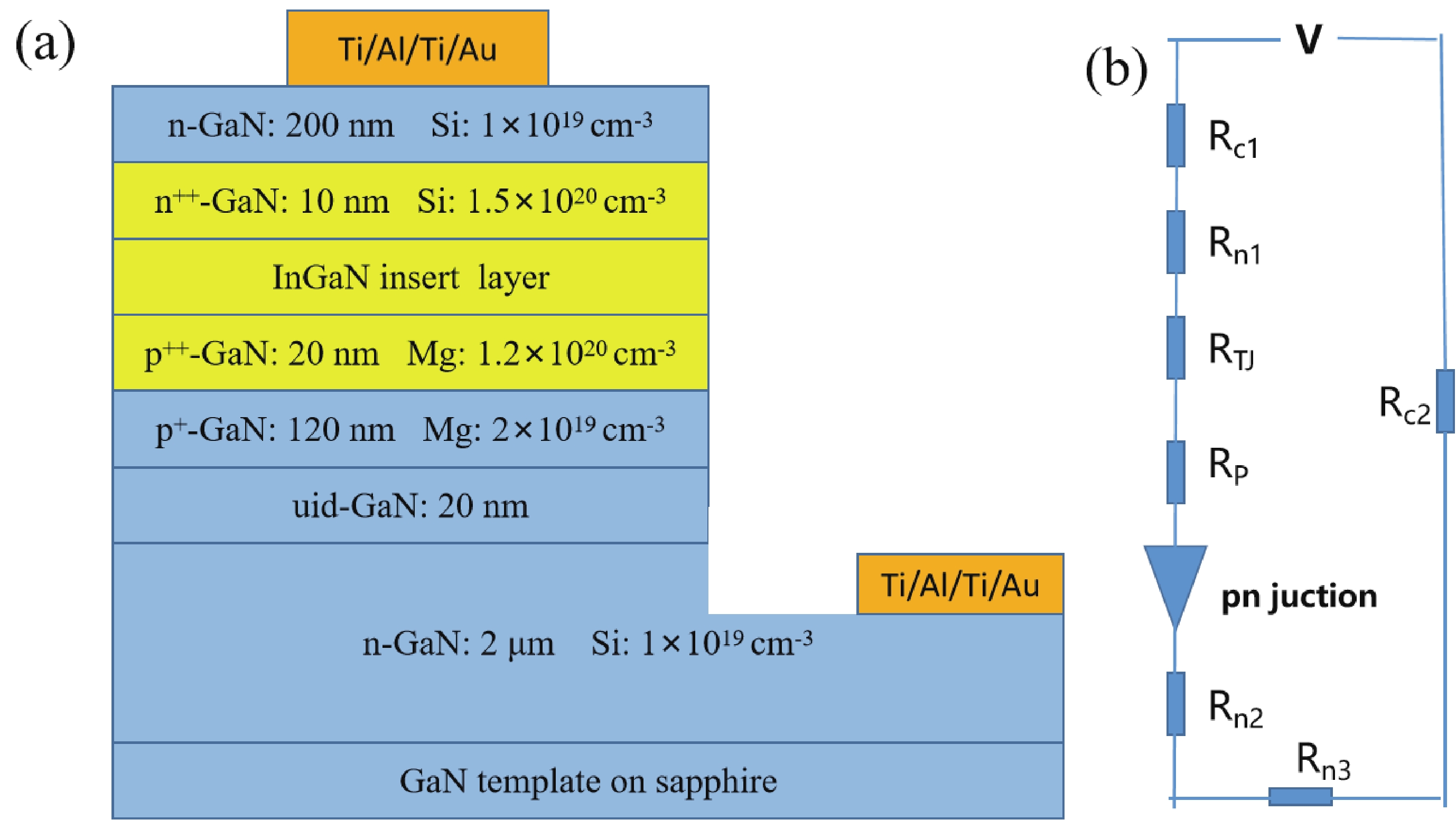
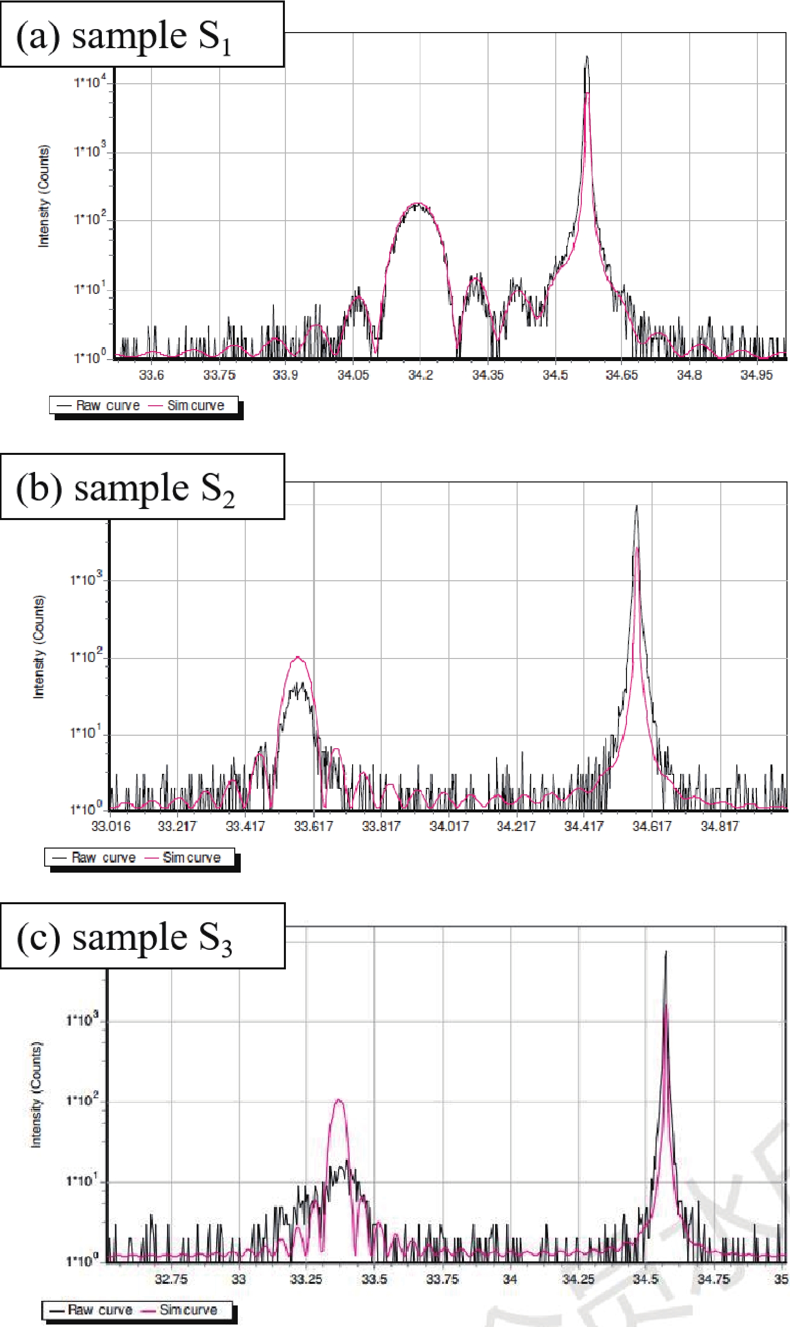
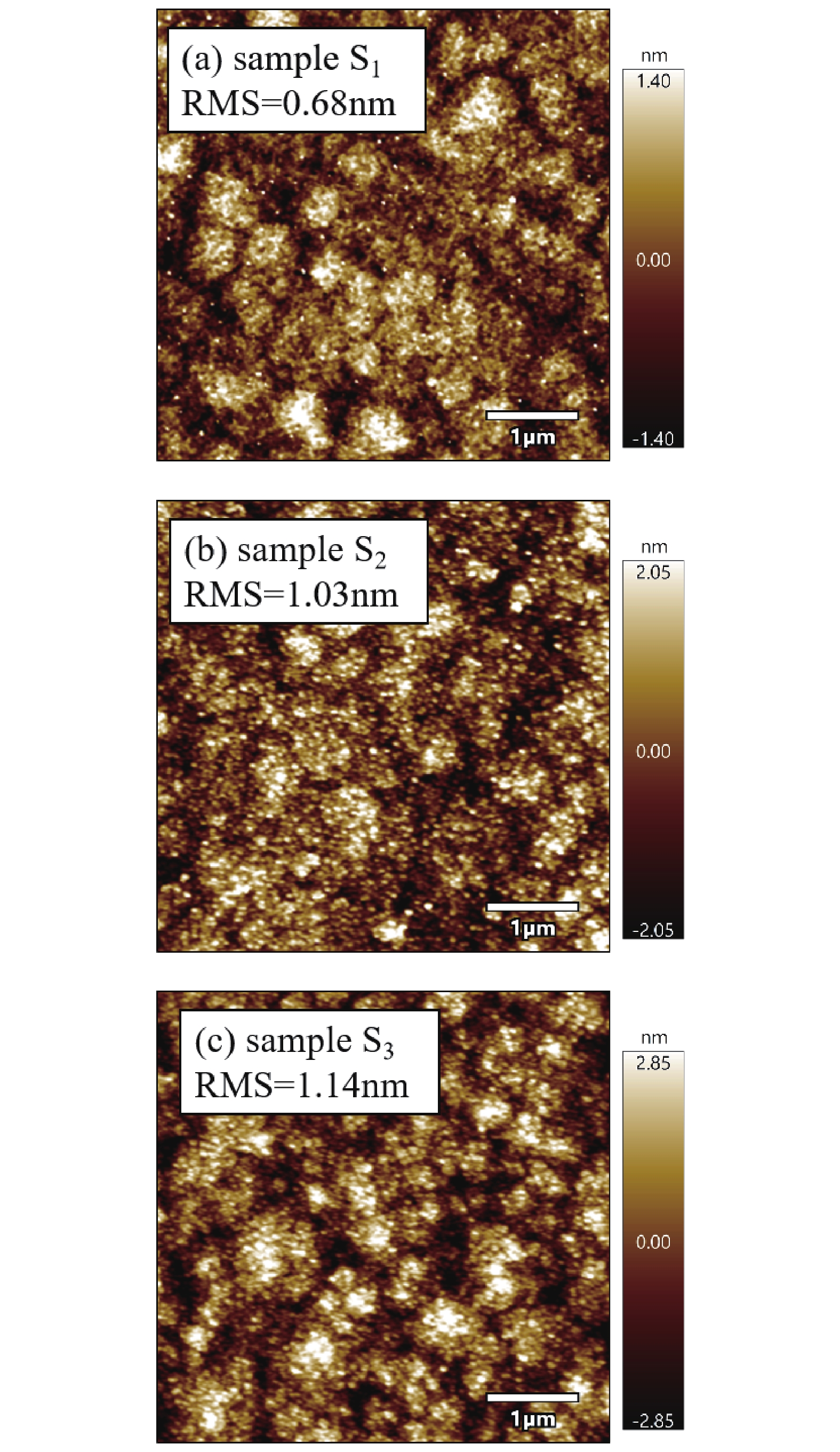
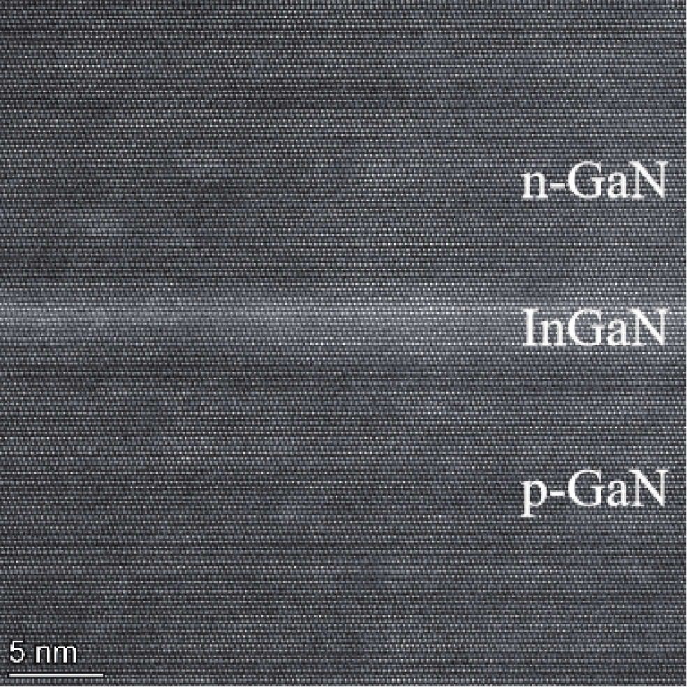
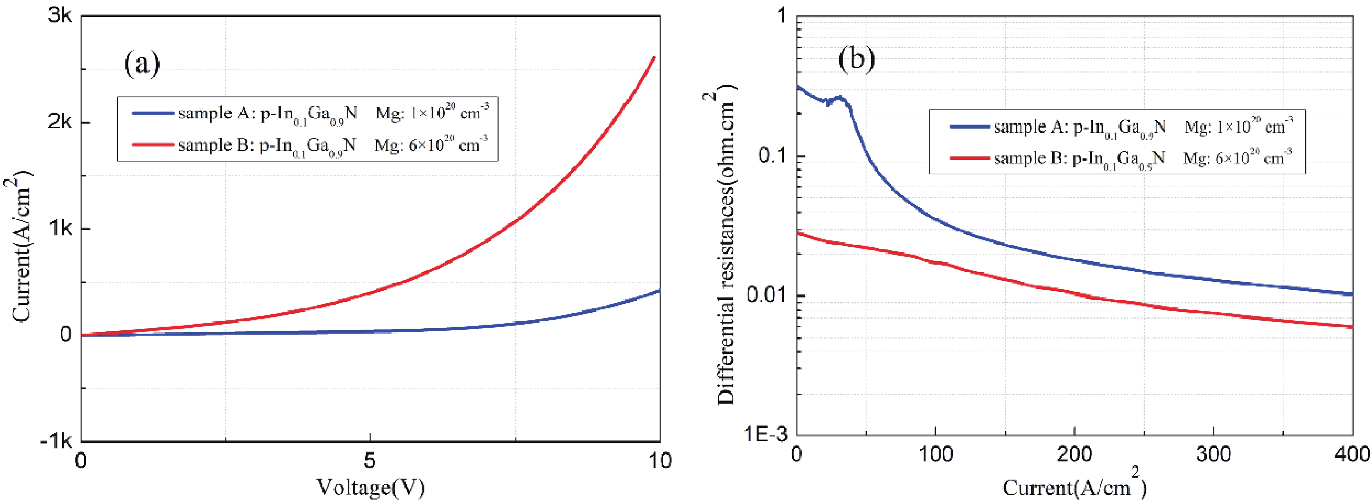
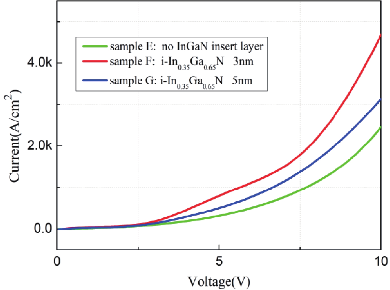
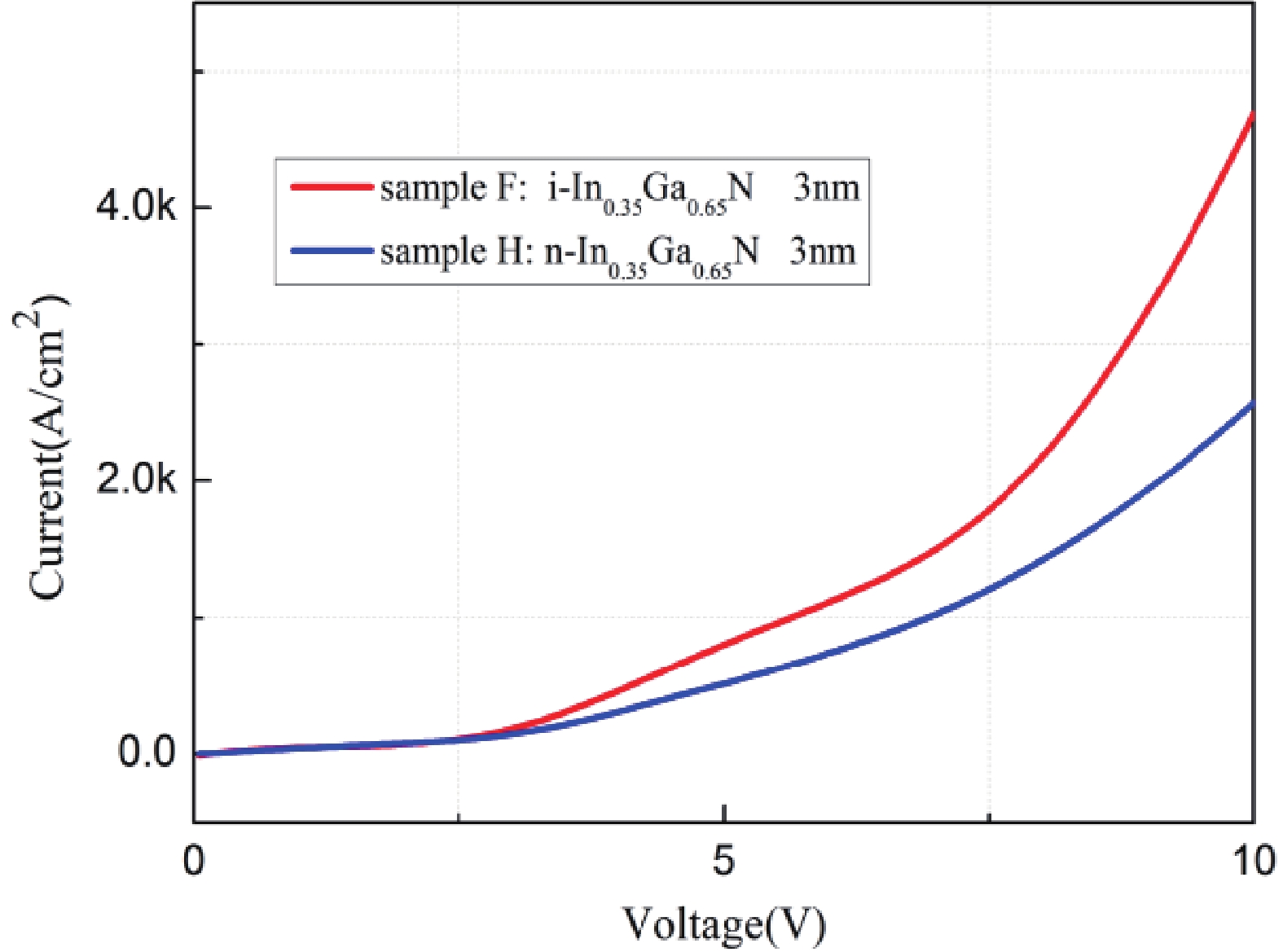
The InGaN films and GaN/InGaN/GaN tunnel junctions (TJs) were grown on GaN templates with plasma-assisted molecular beam epitaxy. As the In content increases, the quality of InGaN films grown on GaN templates decreases and the surface roughness of the samples increases. V-pits and trench defects were not found in the AFM images. p++-GaN/InGaN/n++-GaN TJs were investigated for various In content, InGaN thicknesses and doping concentration in the InGaN insert layer. The InGaN insert layer can promote good interband tunneling in GaN/InGaN/GaN TJ and significantly reduce operating voltage when doping is sufficiently high. The current density increases with increasing In content for the 3 nm InGaN insert layer, which is achieved by reducing the depletion zone width and the height of the potential barrier. At a forward current density of 500 A/cm2, the measured voltage was 4.31 V and the differential resistance was measured to be 3.75 × 10⁻³ Ω·cm2 for the device with a 3 nm p++-In0.35Ga0.65N insert layer. When the thickness of the In0.35Ga0.65N layer is closer to the “balanced” thickness, the TJ current density is higher. If the thickness is too high or too low, the width of the depletion zone will increase and the current density will decrease. The undoped InGaN layer has a better performance than n-type doping in the TJ. Polarization-engineered tunnel junctions can enhance the functionality and performance of electronic and optoelectronic devices.

J. Semicond.
2024, 45(1): 012504 doi: 10.1088/1674-4926/45/1/012504
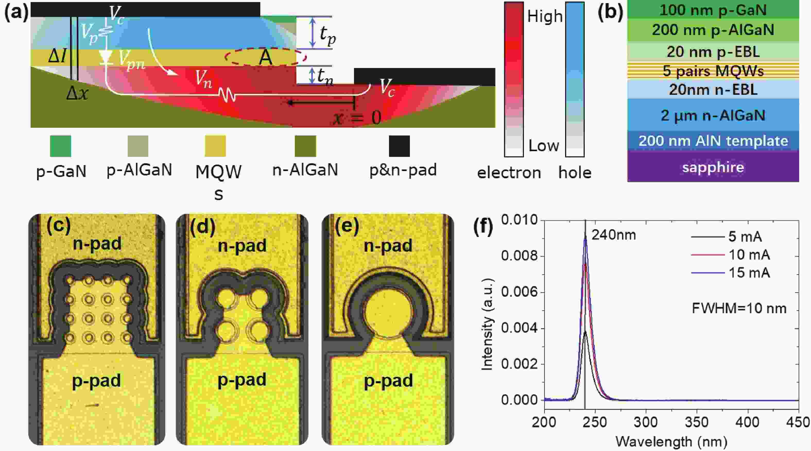
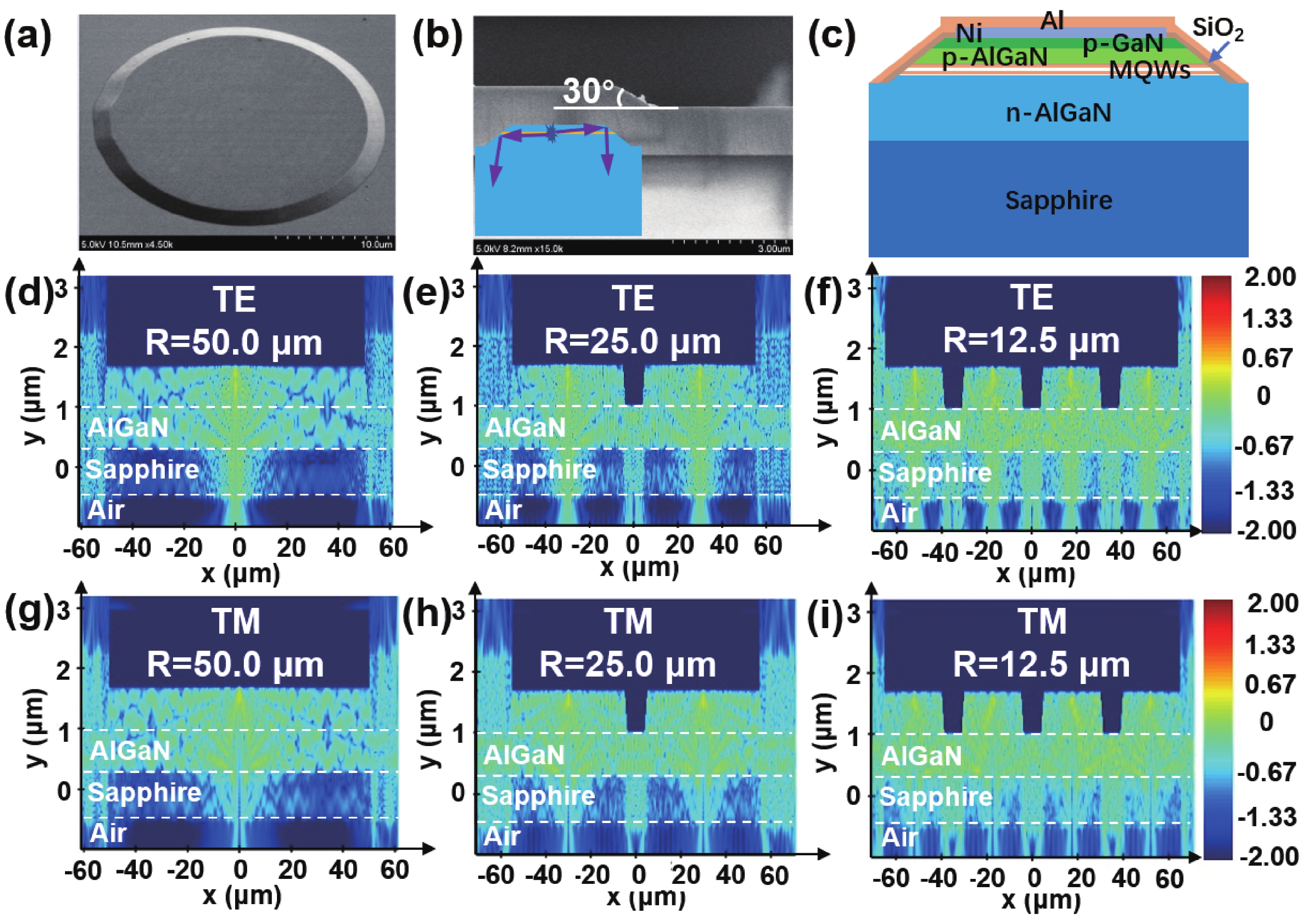
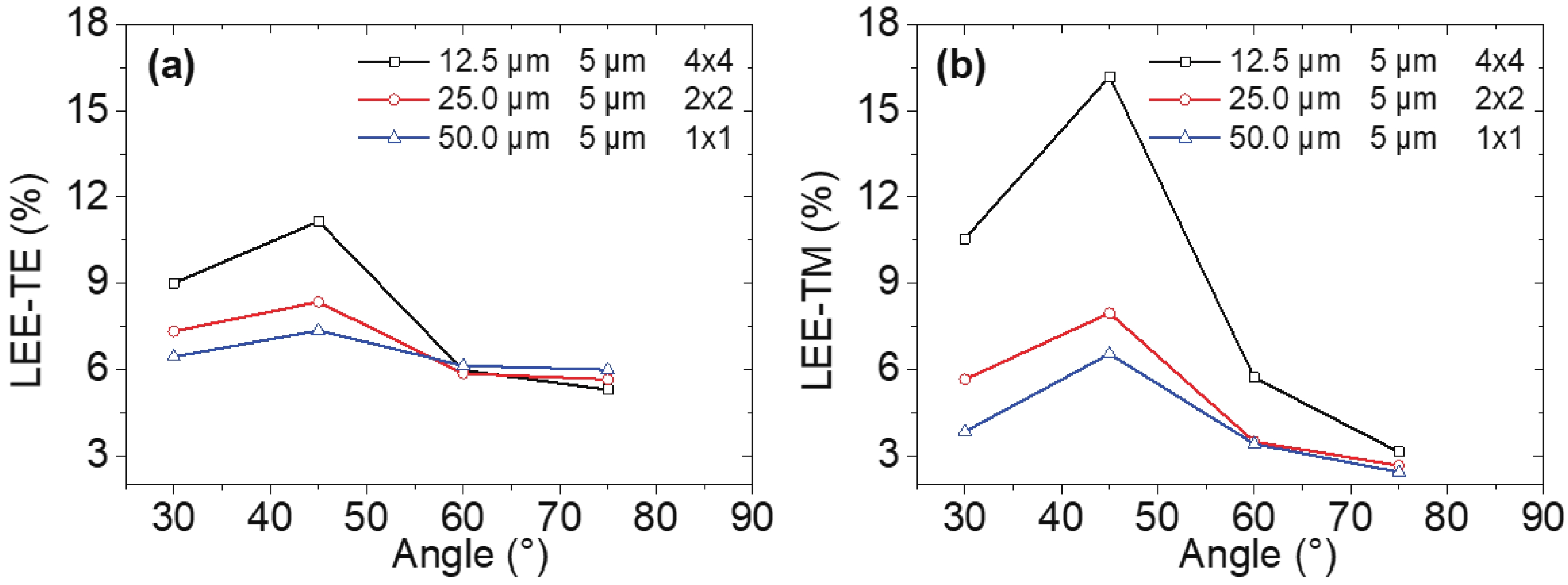
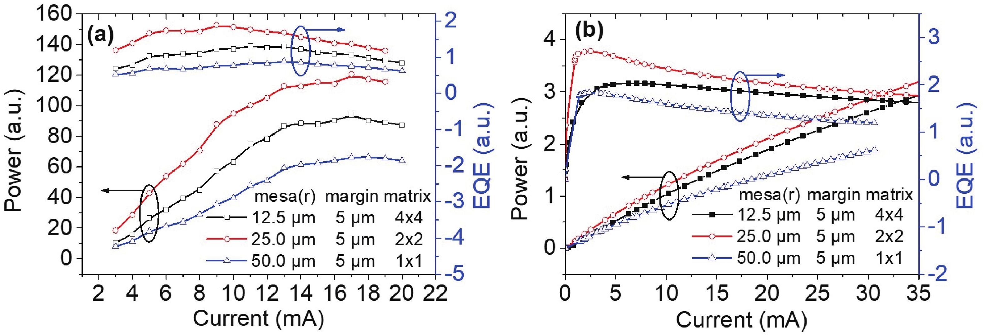
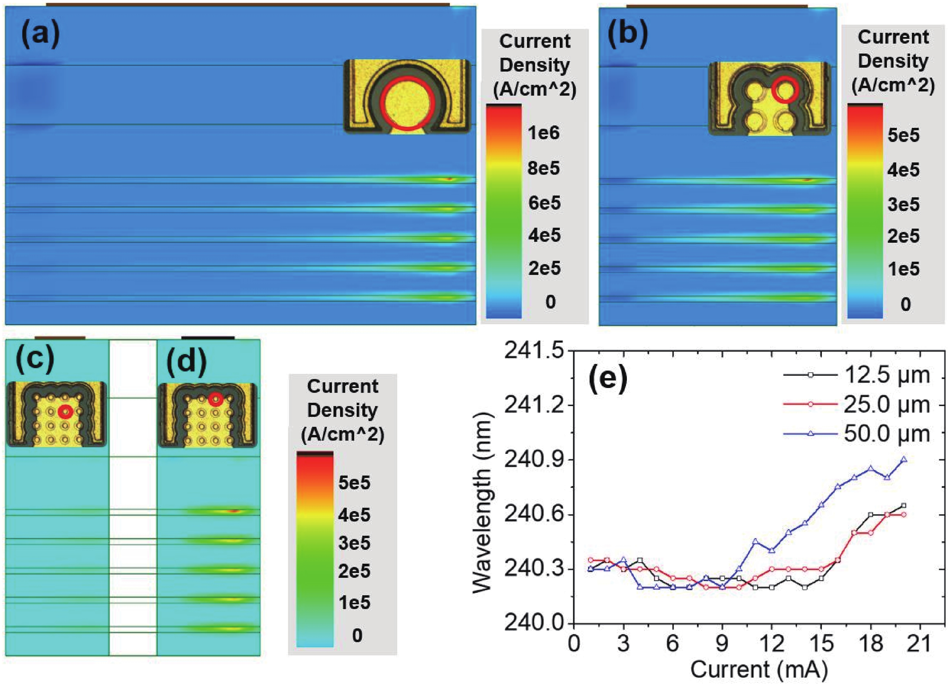
240 nm AlGaN-based micro-LEDs with different sizes are designed and fabricated. Then, the external quantum efficiency (EQE) and light extraction efficiency (LEE) are systematically investigated by comparing size and edge effects. Here, it is revealed that the peak optical output power increases by 81.83% with the size shrinking from 50.0 to 25.0 μm. Thereinto, the LEE increases by 26.21% and the LEE enhancement mainly comes from the sidewall light extraction. Most notably, transverse-magnetic (TM) mode light intensifies faster as the size shrinks due to the tilted mesa side-wall and Al reflector design. However, when it turns to 12.5 μm sized micro-LEDs, the output power is lower than 25.0 μm sized ones. The underlying mechanism is that even though protected by SiO2 passivation, the edge effect which leads to current leakage and Shockley-Read-Hall (SRH) recombination deteriorates rapidly with the size further shrinking. Moreover, the ratio of the p-contact area to mesa area is much lower, which deteriorates the p-type current spreading at the mesa edge. These findings show a role of thumb for the design of high efficiency micro-LEDs with wavelength below 250 nm, which will pave the way for wide applications of deep ultraviolet (DUV) micro-LEDs.

J. Semicond.
2024, 45(1): 012701 doi: 10.1088/1674-4926/45/1/012701
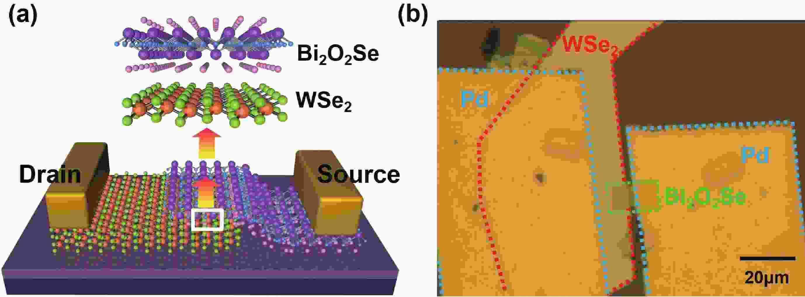
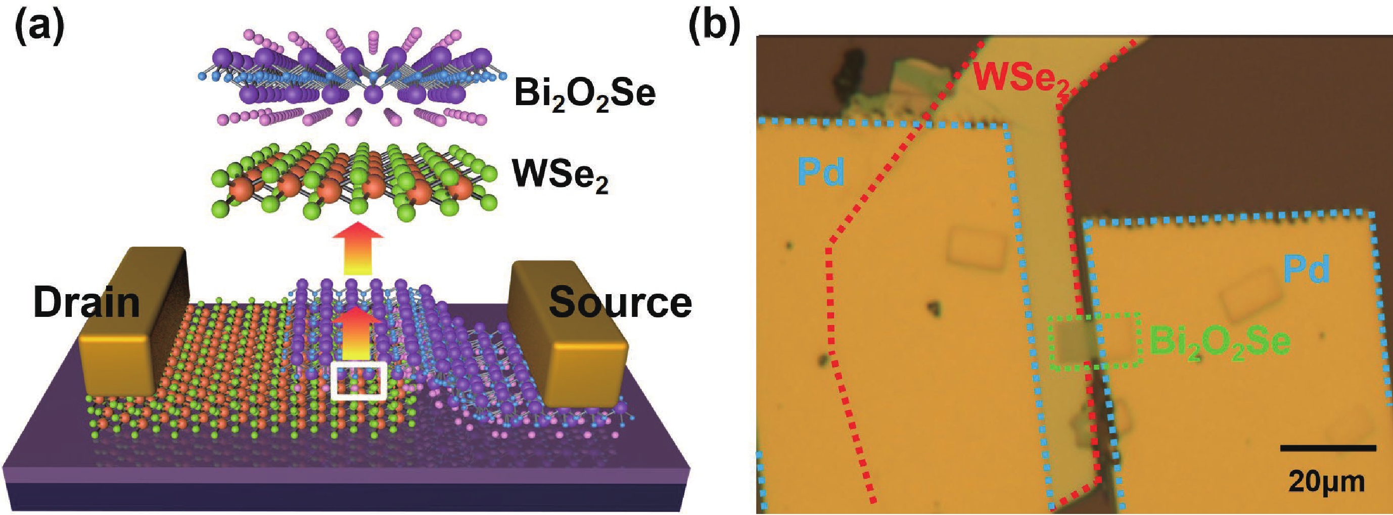
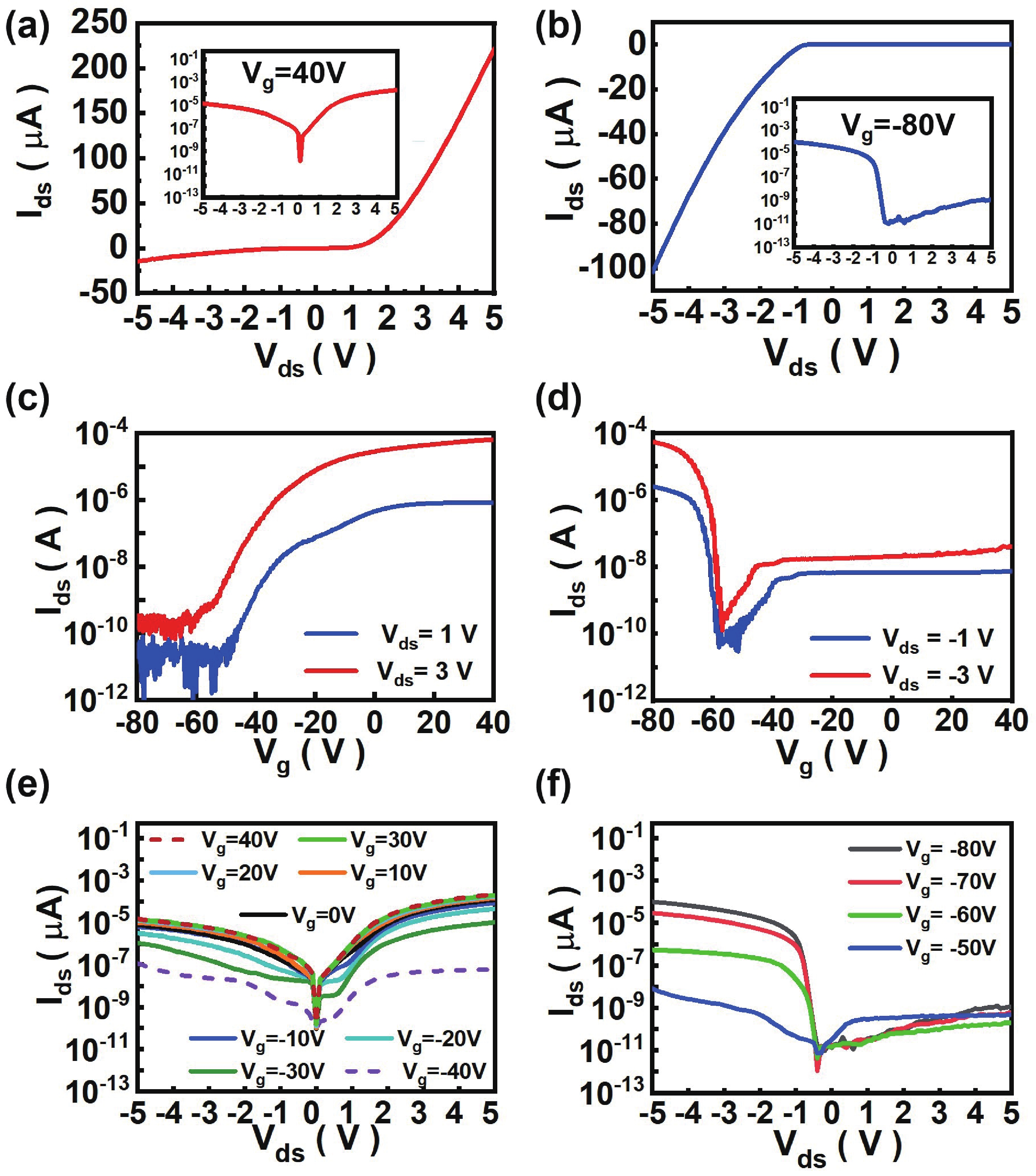
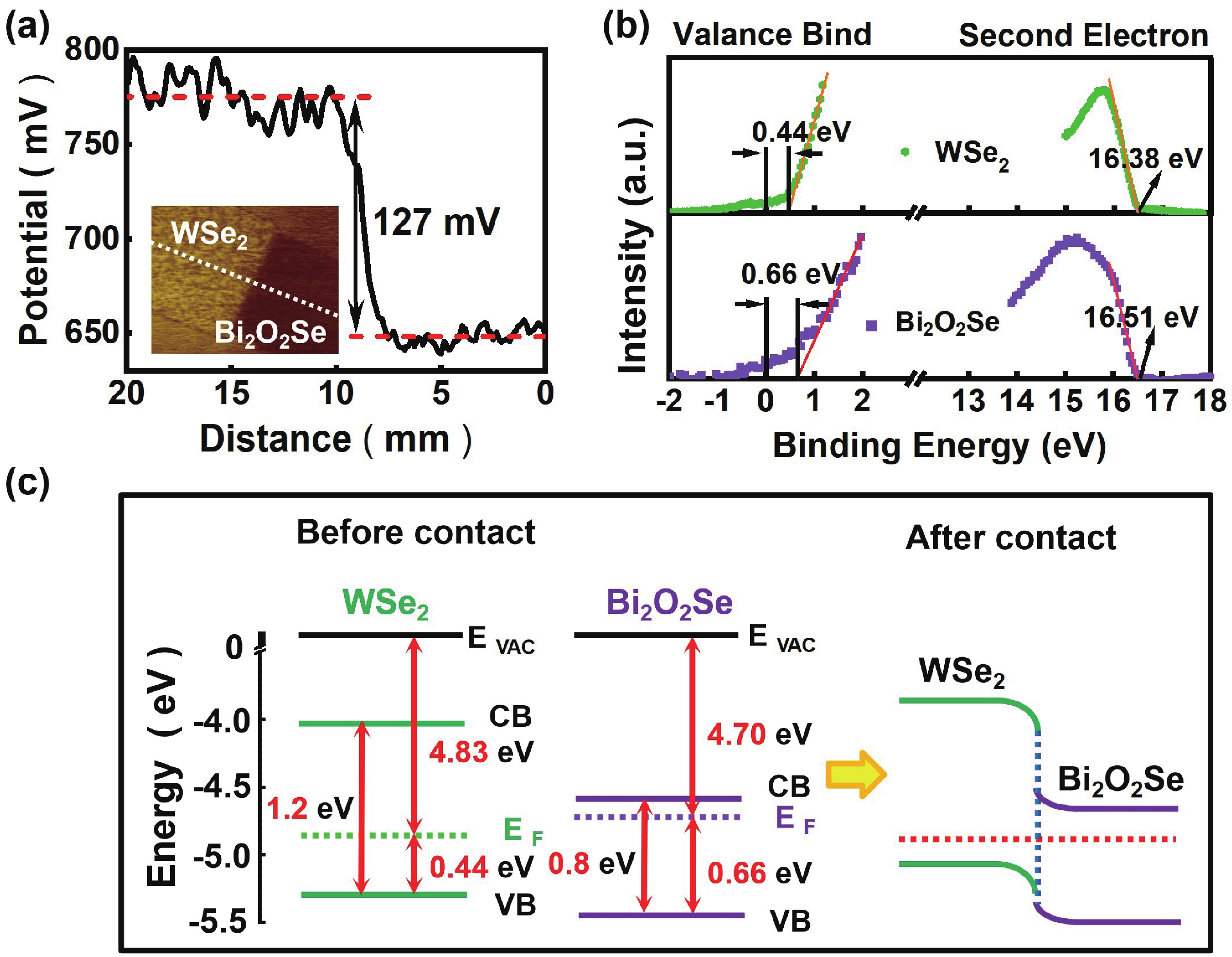
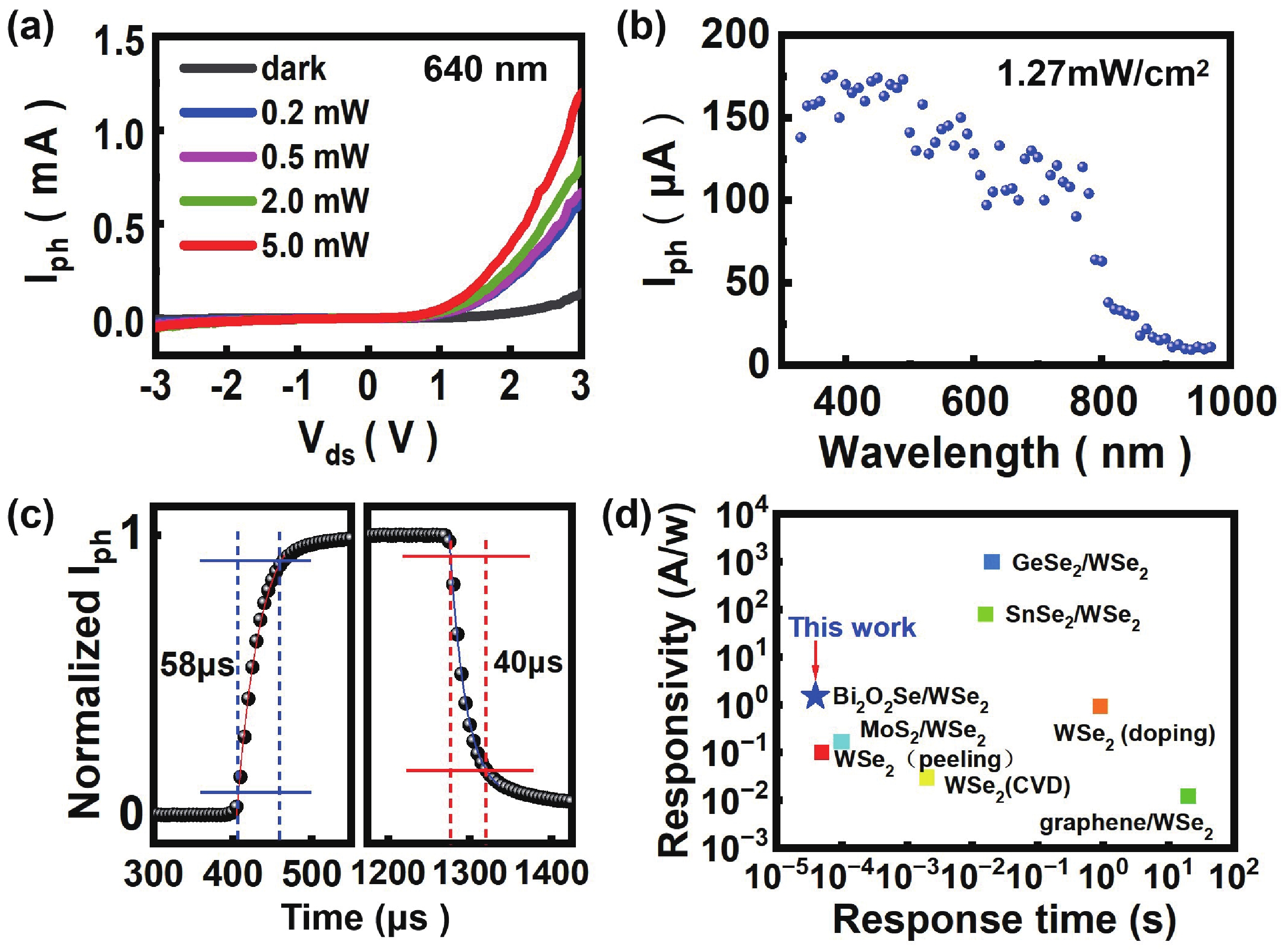
Two-dimensional (2D) WSe2 has received increasing attention due to its unique optical properties and bipolar behavior. Several WSe2-based heterojunctions exhibit bidirectional rectification characteristics, but most devices have a lower rectification ratio. In this work, the Bi2O2Se/WSe2 heterojunction prepared by us has a type Ⅱ band alignment, which can vastly suppress the channel current through the interface barrier so that the Bi2O2Se/WSe2 heterojunction device has a large rectification ratio of about 105. Meanwhile, under different gate voltage modulation, the current on/off ratio of the device changes by nearly five orders of magnitude, and the maximum current on/off ratio is expected to be achieved 106. The photocurrent measurement reveals the behavior of recombination and space charge confinement, further verifying the bidirectional rectification behavior of heterojunctions, and it also exhibits excellent performance in light response. In the future, Bi2O2Se/WSe2 heterojunction field-effect transistors have great potential to reduce the volume of integrated circuits as a bidirectional controlled switching device.